EP1459332B1 - Procede pour produire une couche resistive electroconductrice et dispositif de chauffage et/ou de refroidissement - Google Patents
Procede pour produire une couche resistive electroconductrice et dispositif de chauffage et/ou de refroidissement Download PDFInfo
- Publication number
- EP1459332B1 EP1459332B1 EP02796639A EP02796639A EP1459332B1 EP 1459332 B1 EP1459332 B1 EP 1459332B1 EP 02796639 A EP02796639 A EP 02796639A EP 02796639 A EP02796639 A EP 02796639A EP 1459332 B1 EP1459332 B1 EP 1459332B1
- Authority
- EP
- European Patent Office
- Prior art keywords
- electrically conductive
- layer
- resistor layer
- spraying
- conductive resistor
- Prior art date
- Legal status (The legal status is an assumption and is not a legal conclusion. Google has not performed a legal analysis and makes no representation as to the accuracy of the status listed.)
- Expired - Lifetime
Links
Images

Classifications
-
- C—CHEMISTRY; METALLURGY
- C23—COATING METALLIC MATERIAL; COATING MATERIAL WITH METALLIC MATERIAL; CHEMICAL SURFACE TREATMENT; DIFFUSION TREATMENT OF METALLIC MATERIAL; COATING BY VACUUM EVAPORATION, BY SPUTTERING, BY ION IMPLANTATION OR BY CHEMICAL VAPOUR DEPOSITION, IN GENERAL; INHIBITING CORROSION OF METALLIC MATERIAL OR INCRUSTATION IN GENERAL
- C23C—COATING METALLIC MATERIAL; COATING MATERIAL WITH METALLIC MATERIAL; SURFACE TREATMENT OF METALLIC MATERIAL BY DIFFUSION INTO THE SURFACE, BY CHEMICAL CONVERSION OR SUBSTITUTION; COATING BY VACUUM EVAPORATION, BY SPUTTERING, BY ION IMPLANTATION OR BY CHEMICAL VAPOUR DEPOSITION, IN GENERAL
- C23C4/00—Coating by spraying the coating material in the molten state, e.g. by flame, plasma or electric discharge
- C23C4/01—Selective coating, e.g. pattern coating, without pre-treatment of the material to be coated
-
- C—CHEMISTRY; METALLURGY
- C23—COATING METALLIC MATERIAL; COATING MATERIAL WITH METALLIC MATERIAL; CHEMICAL SURFACE TREATMENT; DIFFUSION TREATMENT OF METALLIC MATERIAL; COATING BY VACUUM EVAPORATION, BY SPUTTERING, BY ION IMPLANTATION OR BY CHEMICAL VAPOUR DEPOSITION, IN GENERAL; INHIBITING CORROSION OF METALLIC MATERIAL OR INCRUSTATION IN GENERAL
- C23C—COATING METALLIC MATERIAL; COATING MATERIAL WITH METALLIC MATERIAL; SURFACE TREATMENT OF METALLIC MATERIAL BY DIFFUSION INTO THE SURFACE, BY CHEMICAL CONVERSION OR SUBSTITUTION; COATING BY VACUUM EVAPORATION, BY SPUTTERING, BY ION IMPLANTATION OR BY CHEMICAL VAPOUR DEPOSITION, IN GENERAL
- C23C24/00—Coating starting from inorganic powder
- C23C24/02—Coating starting from inorganic powder by application of pressure only
- C23C24/04—Impact or kinetic deposition of particles
-
- C—CHEMISTRY; METALLURGY
- C23—COATING METALLIC MATERIAL; COATING MATERIAL WITH METALLIC MATERIAL; CHEMICAL SURFACE TREATMENT; DIFFUSION TREATMENT OF METALLIC MATERIAL; COATING BY VACUUM EVAPORATION, BY SPUTTERING, BY ION IMPLANTATION OR BY CHEMICAL VAPOUR DEPOSITION, IN GENERAL; INHIBITING CORROSION OF METALLIC MATERIAL OR INCRUSTATION IN GENERAL
- C23C—COATING METALLIC MATERIAL; COATING MATERIAL WITH METALLIC MATERIAL; SURFACE TREATMENT OF METALLIC MATERIAL BY DIFFUSION INTO THE SURFACE, BY CHEMICAL CONVERSION OR SUBSTITUTION; COATING BY VACUUM EVAPORATION, BY SPUTTERING, BY ION IMPLANTATION OR BY CHEMICAL VAPOUR DEPOSITION, IN GENERAL
- C23C30/00—Coating with metallic material characterised only by the composition of the metallic material, i.e. not characterised by the coating process
-
- C—CHEMISTRY; METALLURGY
- C23—COATING METALLIC MATERIAL; COATING MATERIAL WITH METALLIC MATERIAL; CHEMICAL SURFACE TREATMENT; DIFFUSION TREATMENT OF METALLIC MATERIAL; COATING BY VACUUM EVAPORATION, BY SPUTTERING, BY ION IMPLANTATION OR BY CHEMICAL VAPOUR DEPOSITION, IN GENERAL; INHIBITING CORROSION OF METALLIC MATERIAL OR INCRUSTATION IN GENERAL
- C23C—COATING METALLIC MATERIAL; COATING MATERIAL WITH METALLIC MATERIAL; SURFACE TREATMENT OF METALLIC MATERIAL BY DIFFUSION INTO THE SURFACE, BY CHEMICAL CONVERSION OR SUBSTITUTION; COATING BY VACUUM EVAPORATION, BY SPUTTERING, BY ION IMPLANTATION OR BY CHEMICAL VAPOUR DEPOSITION, IN GENERAL
- C23C4/00—Coating by spraying the coating material in the molten state, e.g. by flame, plasma or electric discharge
- C23C4/04—Coating by spraying the coating material in the molten state, e.g. by flame, plasma or electric discharge characterised by the coating material
- C23C4/06—Metallic material
-
- C—CHEMISTRY; METALLURGY
- C23—COATING METALLIC MATERIAL; COATING MATERIAL WITH METALLIC MATERIAL; CHEMICAL SURFACE TREATMENT; DIFFUSION TREATMENT OF METALLIC MATERIAL; COATING BY VACUUM EVAPORATION, BY SPUTTERING, BY ION IMPLANTATION OR BY CHEMICAL VAPOUR DEPOSITION, IN GENERAL; INHIBITING CORROSION OF METALLIC MATERIAL OR INCRUSTATION IN GENERAL
- C23C—COATING METALLIC MATERIAL; COATING MATERIAL WITH METALLIC MATERIAL; SURFACE TREATMENT OF METALLIC MATERIAL BY DIFFUSION INTO THE SURFACE, BY CHEMICAL CONVERSION OR SUBSTITUTION; COATING BY VACUUM EVAPORATION, BY SPUTTERING, BY ION IMPLANTATION OR BY CHEMICAL VAPOUR DEPOSITION, IN GENERAL
- C23C4/00—Coating by spraying the coating material in the molten state, e.g. by flame, plasma or electric discharge
- C23C4/04—Coating by spraying the coating material in the molten state, e.g. by flame, plasma or electric discharge characterised by the coating material
- C23C4/06—Metallic material
- C23C4/08—Metallic material containing only metal elements
-
- C—CHEMISTRY; METALLURGY
- C23—COATING METALLIC MATERIAL; COATING MATERIAL WITH METALLIC MATERIAL; CHEMICAL SURFACE TREATMENT; DIFFUSION TREATMENT OF METALLIC MATERIAL; COATING BY VACUUM EVAPORATION, BY SPUTTERING, BY ION IMPLANTATION OR BY CHEMICAL VAPOUR DEPOSITION, IN GENERAL; INHIBITING CORROSION OF METALLIC MATERIAL OR INCRUSTATION IN GENERAL
- C23C—COATING METALLIC MATERIAL; COATING MATERIAL WITH METALLIC MATERIAL; SURFACE TREATMENT OF METALLIC MATERIAL BY DIFFUSION INTO THE SURFACE, BY CHEMICAL CONVERSION OR SUBSTITUTION; COATING BY VACUUM EVAPORATION, BY SPUTTERING, BY ION IMPLANTATION OR BY CHEMICAL VAPOUR DEPOSITION, IN GENERAL
- C23C4/00—Coating by spraying the coating material in the molten state, e.g. by flame, plasma or electric discharge
- C23C4/12—Coating by spraying the coating material in the molten state, e.g. by flame, plasma or electric discharge characterised by the method of spraying
- C23C4/14—Coating by spraying the coating material in the molten state, e.g. by flame, plasma or electric discharge characterised by the method of spraying for coating elongate material
- C23C4/16—Wires; Tubes
-
- C—CHEMISTRY; METALLURGY
- C23—COATING METALLIC MATERIAL; COATING MATERIAL WITH METALLIC MATERIAL; CHEMICAL SURFACE TREATMENT; DIFFUSION TREATMENT OF METALLIC MATERIAL; COATING BY VACUUM EVAPORATION, BY SPUTTERING, BY ION IMPLANTATION OR BY CHEMICAL VAPOUR DEPOSITION, IN GENERAL; INHIBITING CORROSION OF METALLIC MATERIAL OR INCRUSTATION IN GENERAL
- C23C—COATING METALLIC MATERIAL; COATING MATERIAL WITH METALLIC MATERIAL; SURFACE TREATMENT OF METALLIC MATERIAL BY DIFFUSION INTO THE SURFACE, BY CHEMICAL CONVERSION OR SUBSTITUTION; COATING BY VACUUM EVAPORATION, BY SPUTTERING, BY ION IMPLANTATION OR BY CHEMICAL VAPOUR DEPOSITION, IN GENERAL
- C23C4/00—Coating by spraying the coating material in the molten state, e.g. by flame, plasma or electric discharge
- C23C4/18—After-treatment
-
- F—MECHANICAL ENGINEERING; LIGHTING; HEATING; WEAPONS; BLASTING
- F24—HEATING; RANGES; VENTILATING
- F24H—FLUID HEATERS, e.g. WATER OR AIR HEATERS, HAVING HEAT-GENERATING MEANS, e.g. HEAT PUMPS, IN GENERAL
- F24H1/00—Water heaters, e.g. boilers, continuous-flow heaters or water-storage heaters
- F24H1/10—Continuous-flow heaters, i.e. heaters in which heat is generated only while the water is flowing, e.g. with direct contact of the water with the heating medium
- F24H1/12—Continuous-flow heaters, i.e. heaters in which heat is generated only while the water is flowing, e.g. with direct contact of the water with the heating medium in which the water is kept separate from the heating medium
- F24H1/14—Continuous-flow heaters, i.e. heaters in which heat is generated only while the water is flowing, e.g. with direct contact of the water with the heating medium in which the water is kept separate from the heating medium by tubes, e.g. bent in serpentine form
- F24H1/142—Continuous-flow heaters, i.e. heaters in which heat is generated only while the water is flowing, e.g. with direct contact of the water with the heating medium in which the water is kept separate from the heating medium by tubes, e.g. bent in serpentine form using electric energy supply
-
- H—ELECTRICITY
- H01—ELECTRIC ELEMENTS
- H01C—RESISTORS
- H01C17/00—Apparatus or processes specially adapted for manufacturing resistors
- H01C17/22—Apparatus or processes specially adapted for manufacturing resistors adapted for trimming
- H01C17/24—Apparatus or processes specially adapted for manufacturing resistors adapted for trimming by removing or adding resistive material
-
- H—ELECTRICITY
- H01—ELECTRIC ELEMENTS
- H01C—RESISTORS
- H01C17/00—Apparatus or processes specially adapted for manufacturing resistors
- H01C17/22—Apparatus or processes specially adapted for manufacturing resistors adapted for trimming
- H01C17/24—Apparatus or processes specially adapted for manufacturing resistors adapted for trimming by removing or adding resistive material
- H01C17/245—Apparatus or processes specially adapted for manufacturing resistors adapted for trimming by removing or adding resistive material by mechanical means, e.g. sand-blasting, cutting or ultrasonic treatment
-
- H—ELECTRICITY
- H05—ELECTRIC TECHNIQUES NOT OTHERWISE PROVIDED FOR
- H05B—ELECTRIC HEATING; ELECTRIC LIGHT SOURCES NOT OTHERWISE PROVIDED FOR; CIRCUIT ARRANGEMENTS FOR ELECTRIC LIGHT SOURCES, IN GENERAL
- H05B3/00—Ohmic-resistance heating
- H05B3/40—Heating elements having the shape of rods or tubes
- H05B3/42—Heating elements having the shape of rods or tubes non-flexible
- H05B3/46—Heating elements having the shape of rods or tubes non-flexible heating conductor mounted on insulating base
-
- Y—GENERAL TAGGING OF NEW TECHNOLOGICAL DEVELOPMENTS; GENERAL TAGGING OF CROSS-SECTIONAL TECHNOLOGIES SPANNING OVER SEVERAL SECTIONS OF THE IPC; TECHNICAL SUBJECTS COVERED BY FORMER USPC CROSS-REFERENCE ART COLLECTIONS [XRACs] AND DIGESTS
- Y10—TECHNICAL SUBJECTS COVERED BY FORMER USPC
- Y10T—TECHNICAL SUBJECTS COVERED BY FORMER US CLASSIFICATION
- Y10T29/00—Metal working
- Y10T29/49—Method of mechanical manufacture
- Y10T29/49002—Electrical device making
- Y10T29/49082—Resistor making
- Y10T29/49083—Heater type
-
- Y—GENERAL TAGGING OF NEW TECHNOLOGICAL DEVELOPMENTS; GENERAL TAGGING OF CROSS-SECTIONAL TECHNOLOGIES SPANNING OVER SEVERAL SECTIONS OF THE IPC; TECHNICAL SUBJECTS COVERED BY FORMER USPC CROSS-REFERENCE ART COLLECTIONS [XRACs] AND DIGESTS
- Y10—TECHNICAL SUBJECTS COVERED BY FORMER USPC
- Y10T—TECHNICAL SUBJECTS COVERED BY FORMER US CLASSIFICATION
- Y10T29/00—Metal working
- Y10T29/49—Method of mechanical manufacture
- Y10T29/49002—Electrical device making
- Y10T29/49082—Resistor making
- Y10T29/49099—Coating resistive material on a base
Definitions
- the invention relates to a method for producing an electrically conductive resistance layer, with the features of the preamble of claim 1.
- the invention also relates to a heating and / or cooling device having the features of the preamble of claim 11.
- Such a method is from the DE 198 10 848 A1 known.
- a heating element is described, which is produced by applying band-shaped layers of an electrically conductive and a resistance-forming material on surfaces of a substrate by means of arc sputtering or by plasma spraying.
- a release liner is previously applied to the substrate by means of a printing process.
- the release liner is made of such a material that the electrically conductive material does not adhere to those locations of the substrate where the release liner is present.
- the known method has the roof part that it is relatively expensive and therefore the parts with the electrically conductive resistance layers are relatively expensive. Furthermore can be provided with an electrically conductive layer only more or less flat parts with the known method.
- the present invention therefore has the object of developing a method of the type mentioned so that the production of an electrically conductive layer on a substrate is easier and cheaper possible and also complex shaped objects can be provided with such an electrically conductive resistance layer, wherein the resistor should be set as accurately as possible.
- the electrically conductive material of which the resistance layer is made is applied flat and generally uniformly on the non-conductive substrate.
- the application by means of thermal spraying ensures a high adhesion of the electrically conductive material on the non-conductive surface.
- the A variety of materials can be applied quickly and very evenly on the non-conductive substrate in this way.
- the applied electrically conductive material is removed at certain points by means of a suitable device. As a result, a complex shaping of the electrically conductive layer is made possible in only two steps.
- Plasma spraying, high-speed flame spraying, arc spraying, autogenous spraying, laser spraying or cold gas spraying has proven to be favorable for the application of the electrically conductive material to the substrate.
- the invention provides that the local electrical resistance of the electrically conductive resistance layer is adjusted by a local heat treatment. By heating locally oxides can be registered in the layer, which has an effect on the local electrical conductivity of the material. This allows a special. Precise and fine adjustment of the electrical resistance.
- a further development provides that the removal of the material layer in regions takes place by means of laser radiation or by means of a water jet or by means of a powder sand blast.
- the material When using laser radiation, the material is heated so much that it evaporates.
- the use of a Laser beam has the advantage that it very quickly very high energies can be coupled into the electrically conductive material so that it evaporates immediately. This instantaneous evaporation of the electrically conductive material ensures that only comparatively little heat is coupled into the substrate present under the electrically conductive material. This is therefore not damaged in the method according to the invention.
- the evaporation has the advantage over incineration that essentially no residues remain in the evaporated areas on the substrate and so their insulation is very good.
- the electrical resistance of the electrically conductive resistance layer is detected at least indirectly during the area-wise removal of the material layer. In this way, a precise quality control is already possible directly during the production of the electrically conductive layer.
- an actual value of the electrical resistance of the electrically conductive resistance layer is compared with a target value and the electrical resistance of the electrically conductive layer is changed by removal of additional electrically conductive material in regions such that the difference between actual value and desired value is reduced.
- Such deviations may, for example, be the result of different amounts of the electrically conductive material reaching the substrate during spraying of the thermally conductive material, so that the resulting electrically conductive layer has a different thickness at one point than at another location.
- deviations of the actual value of the electrical resistance of the electrically conductive layer from the desired value can be compensated for with an accuracy of +/- 1%.
- the partial removal of additional electrically conductive material may include a shortening or lengthening of the electrically conductive layer and / or the variation of the width of the electrically conductive layer.
- the material layer is removed in such a way that a desired melting point in the sense of a fuse is produced at at least one point of the electrically conductive layer.
- a desired melting point in the sense of a fuse is produced at at least one point of the electrically conductive layer.
- the material layer is removed in such a way that the electrically conductive resistance layer is at least partially meandering. This allows the formation of as long as possible electrically conductive resistance layer on a small area.
- the electrically conductive material preferably comprises bismuth, tellurium, germanium, silicon and / or gallium arsenide. These materials have proved to be particularly favorable for the application by means of thermal spraying and the subsequent processing by means of laser radiation. In addition, with these materials, the relevant known technical effects can be realized.
- the electrically conductive material is applied in this way and the material layer is partially removed in such a way and comprises such a material that an electrical heating or an electrical cooling layer is formed.
- the "Peltier effect" is advantageously utilized.
- the electrically conductive resistance layer is sealed.
- This has particular advantages in a porous substrate (for example, metal with Al 2 O 3 intermediate layer). Sealing reduces the risk of electrical breakdown due to humidity, especially at high voltage.
- a material for sealing silicone, polyimide, or water glass the latter on sodium or potassium-based. The application can be done by dipping, spraying, brushing, etc. The seal of the seal is best when the sealant layer is applied under vacuum.
- non-conductive substrate is also glass or glass ceramic in question.
- the electrical resistance layer can be applied permanently, especially by plasma spraying.
- the good insulating effect of glass makes grounding in the operation of the resistive layer superfluous. It is also possible to use special Fiochtemperaturglas, such as Ceranglas®.
- the invention also relates to a heating and / or cooling device having the features of claim 11, a non-conductive substrate and an applied to the substrate by thermal spraying electrically conductive resistance layer.
- the production costs for such a heating and / or cooling device can be reduced if the resistance layer comprises an electrically conductive material initially applied by thermal spraying, which was then removed in regions by means of laser radiation and thus brought into a desired shape.
- the resistance layer comprises an electrically conductive material initially applied by thermal spraying, which was then removed in regions by means of laser radiation and thus brought into a desired shape.
- such heating and / or cooling devices have precise resistance.
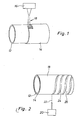
- FIG. 1 and 2 shows the production of a tubular water heater:
- an electrically conductive material layer 14 is applied to a tube 12 made of a high-temperature resistant and an electrical insulator material ( Fig. 1 ).
- the application takes place in the present exemplary embodiment by means of a device 16, with which germanium particles 18 are sprayed onto the tube 12.
- the application is carried out by cold gas spraying (also called "gas-dynamic powder coating").
- the unmelted germanium particles are heated to speeds of about 300 - Accelerated 1,200 m / s and sprayed onto the tube 12.
- the germanium particles 18 and also the surface of the tube 12 deform.
- the impact breaks up surface oxides on the surface of the tube 12. Micro-friction due to the impact increases the temperature at the contact surface and leads to micro-welds.
- the acceleration of the germanium particles 18 takes place by means of a delivery gas, the temperature of which can be slightly increased.
- the germanium powder 18 in no case reaches its melting temperature, the temperatures arising at the surface of the tube 12 are relatively moderate, so that, for example, a comparatively inexpensive plastic material for the tube 12 can be used.
- plasma spraying, high-speed flame spraying, arc spraying, autogenous spraying or laser spraying for applying the electrically conductive material to the substrate can also be used instead of the cold gas spraying.
- germanium, bismuth, tellurium, silicon and / or gallium arsenide are also suitable, depending on the desired technical effect.
- the coating of the tube 12 with the germanium particles 18 is carried out initially so that gradually the entire Surface of the tube 12 is covered with the germanium material layer 14 (see. Fig.1 ).
- this material layer 14 does not yet have the desired shape:
- the laser device 20 on the one hand and a device, not shown in the figure, with which the tube 12 is held, are thereby moved so that a continuous working process by the laser device 20 is possible.
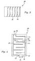
- FIG. 4 shows in plan view a flat heating plate 28.
- This consists of a non-visible in this plan view non-conductive ground, on the analogous to that in the FIGS. 1 and 2 described first, a sheet-like material layer 14 has been applied, were subsequently evaporated from the areas 24 by means of a laser beam (for illustrative purposes, only one area 24 provided with reference numerals).
- a laser beam for illustrative purposes, only one area 24 provided with reference numerals.
- this has two peculiarities:
- a second special feature is that the heating power or the heat flux density of the electrically conductive resistive layer was corrected during its production so that it corresponds to the desired heat output and the desired heat flux density with very high precision. This happens in the following way:
- an electrical voltage is applied during the evaporation of the regions 24, so that the electrical resistance of the electrically conductive layer 26 can be continuously measured during this evaporation.
- the material layer 14 is evaporated only in initially very narrow regions 24.
- horizontally extending evaporated areas 24 thus initially run only from one in Fig. 4 Dashed edge 36 shown up to the overlying horizontal edge 38 of the electrically conductive resistance layer 26 (here, too, for representation reasons, only in a region 24, the corresponding reference number entered).
- the material layer 14 is first processed by the laser beam so that the in Fig. 4 lower electrical end region 34 is relatively wide. This is also shown by a dashed line by the reference numeral 40.
- the actual electrical resistance WIST (see. Fig. 5 ) of the electrically conductive resistance layer 26 is less than the desired per se electrical resistance WSOLL.
- the in Fig. 4 lower connection region 34 of the electric conductive resistance layer 26 is therefore processed by the laser beam so that its width decreases, so it is evaporated additional material.
- the electrically conductive resistance layer 26 extends by a dimension d1 (cf. Fig. 4 and 5 ) and, as a result, the actual electrical resistance WIST increases until it approximately corresponds to the desired resistance WSOLL.
- the final position of the boundary line of the lower electrical connection 34 carries in Fig. 4 the reference numeral 42.
- a plate-shaped heater is shown in section. In contrast to the embodiments described above, it comprises not only an electrically conductive resistance layer, but two electrically conductive resistance layers 26a and 26b. Between these an electrically non-conductive intermediate layer 46 is present. The production of this electric heating plate 28 takes place as follows:
- an electrically conductive material is applied to a plate-shaped carrier 12.
- the application takes place surface by thermal spraying in such a way that the resulting material layer initially has substantially no desired shape.
- the material layer is partially evaporated by laser radiation (reference numeral 24a) in such a way that an electrically conductive resistance layer 26a is produced, which has the desired shape.
- the electrically insulating intermediate layer 46 is applied in the further course of the manufacturing process. Then the process described above is repeated, i. H. again electrically conductive material is applied by means of thermal spraying onto the non-conductive intermediate layer 46 in such a way that a second material layer formed therefrom substantially does not yet have the desired shape. This is then processed by laser radiation and partially evaporated (reference numeral 24b) such that a second electrically conductive resistance layer (26b) is formed in the desired shape.
- the material of the electrically conductive layer is selected so that instead of an electrical heating layer, an electrical Cooling layer is formed.
- the temperature of the heating layer is monitored by a ceramic switch.
- a ceramic switch This is understood to mean a non-mechanical switch which has an element whose conductivity depends to a considerable extent on its temperature.
- a bimetal switch can be used.
Landscapes
- Chemical & Material Sciences (AREA)
- Engineering & Computer Science (AREA)
- Mechanical Engineering (AREA)
- Organic Chemistry (AREA)
- Chemical Kinetics & Catalysis (AREA)
- Materials Engineering (AREA)
- Metallurgy (AREA)
- Physics & Mathematics (AREA)
- Plasma & Fusion (AREA)
- Microelectronics & Electronic Packaging (AREA)
- Manufacturing & Machinery (AREA)
- Thermal Sciences (AREA)
- Combustion & Propulsion (AREA)
- General Engineering & Computer Science (AREA)
- Coating By Spraying Or Casting (AREA)
- Apparatuses And Processes For Manufacturing Resistors (AREA)
- Resistance Heating (AREA)
- Conductive Materials (AREA)
- Laser Beam Processing (AREA)
Claims (17)
- Procédé de fabrication d'une couche résistive électriquement conductrice (26 ; 26a, 26b), avec lequel une matière électriquement conductrice (16) est appliquée sur un substrat (12 ; 12, 46) non conducteur par projection thermique, projection au plasma, projection de flamme à grande vitesse, projection d'arc électrique, projection à l'autogène, projection laser ou projection de gaz froid (16), sachant que la matière électriquement conductrice (18) est appliquée sur la surface de manière telle qu'une couche de matière (14) ainsi réalisée, d'abord pour l'essentiel, ne présente pas encore une forme souhaitée, et qu'ensuite la couche de matière (14) est supprimée dans certaines zones (24 ; 24a, 24b) de manière telle que soit réalisée une couche résistive électriquement conductrice (26 ; 26a, 26b) qui a pour l'essentiel la forme souhaitée, caractérisé en ce que la résistance électrique locale de la couche résistive électriquement conductrice est ajustée par un traitement thermique local par inclusion locale d'oxydes dans la couche.
- Procédé selon la revendication 1, caractérisé en ce que la suppression dans certaines zones de la couche de matière (14) a lieu au moyen d'un rayonnement laser, d'un jet d'eau ou d'un jet de sable ou de poudre, de sorte que la couche résistive électriquement conductrice (26) ait une forme en particulier de méandre au moins dans certaines zones.
- Procédé selon la revendication 1, caractérisé en ce que, durant la suppression dans certaines zones (24) de la couche de matière (14), la résistance électrique (WIST) de la couche résistive électriquement conductrice (26) est détectée au moins indirectement.
- Procédé selon la revendication 3, caractérisé en ce qu'une valeur réelle (WIST) de la résistance électrique de la couche résistive électriquement conductrice est comparée à une valeur de consigne (WSOLL) et en ce que, par la suppression dans certaines zones (24) de matière électriquement conductrice supplémentaire (38, 42), la résistance électrique (WIST) de la couche résistive électriquement conductrice (26) est modifiée de manière telle que la différence soit réduite entre la valeur réelle (WIST) et la valeur de consigne (WSOLL).
- Procédé selon la revendication 4, caractérisé en ce que la détection de la valeur réelle (WIST) de la résistance électrique de la couche résistive électriquement conductrice et la réduction de la différence entre la valeur réelle (WIST) et la valeur de consigne (WSOLL) ont lieu en parallèle.
- Procédé selon l'une quelconque des revendications précédentes, caractérisé en ce que la couche de matière (14) est supprimée (24) de manière telle qu'au moins en un secteur de la couche résistive électriquement conductrice (26) se crée un secteur de fusion théorique (30) au sens d'un fusible de sécurité.
- Procédé selon l'une quelconque des revendications précédentes, caractérisé en ce que, après la suppression dans certaines zones (24a) de la couche de matière et la réalisation de la couche résistive électriquement conductrice (26a), une couche intermédiaire (46) non conductrice est appliquée sur cette couche résistive électriquement conductrice, puis une matière électriquement conductrice est appliquée sur la surface de la couche intermédiaire (46) non conductrice par projection thermique de manière telle qu'une couche de matière ainsi réalisée d'abord pour l'essentiel ne présente pas encore une forme souhaitée et qu'ensuite la couche de matière soit supprimée dans certaines zones (24b) de manière telle que soit réalisée une deuxième couche résistive électriquement conductrice (26b) qui a la forme souhaitée.
- Procédé selon l'une quelconque des revendications précédentes, caractérisé en ce que la matière électriquement conductrice (18) est appliquée, et la couche de matière (14) est supprimée dans certaines zones (24) et comporte une telle matière au point qu'une couche de chauffage électrique (26) ou une couche de refroidissement électrique soit formée.
- Procédé selon l'une quelconque des revendications précédentes, caractérisé en ce que la couche résistive électriquement conductrice est vitrifiée, en particulier au moyen de silicone, de polyimide ou de verre soluble.
- Procédé selon la revendication 9, caractérisé en ce que la vitrification se fait sous vide.
- Dispositif de chauffage et/ou de refroidissement (28), doté d'un substrat (12 ; 12, 46) non conducteur et d'une couche résistive électriquement conductrice (26 ; 26a, 26b) appliquée sur le substrat (12 ; 12, 46) par projection thermique (16), projection au plasma, projection de flamme à grande vitesse, projection d'arc électrique, projection à l'autogène, projection laser ou projection de gaz froid, laquelle couche comporte une matière électriquement conductrice (18) qui a été d'abord appliquée sur la surface puis supprimée dans certaines zones (24 ; 24a, 24b) et amenée par cela à une forme souhaitée, caractérisé en ce que des oxydes ont été inclus localement dans la couche suite à un traitement thermique local afin d'ajuster la résistance électrique locale de la couche résistive électriquement conductrice (26 ; 26a, 26b).
- Dispositif de chauffage et/ou de refroidissement selon la revendication 11, caractérisé en ce que la couche résistive électriquement conductrice (26 ; 26a, 26b) est vitrifiée.
- Dispositif de chauffage et/ou de refroidissement selon la revendication 11 ou 12, caractérisé en ce que sur la couche résistive électriquement conductrice (26a) réalisée repose une couche intermédiaire (46) non conductrice et en ce que sur la surface de cette dernière repose une deuxième couche résistive électriquement conductrice (26b) pour laquelle la couche de matière a été supprimée dans certaines zones comme pour la couche résistive (26a).
- Dispositif de chauffage et/ou de refroidissement selon l'une quelconque des revendications 11 à 13, caractérisé en ce que plusieurs couches résistives et couches intermédiaires sont disposées les unes au-dessus des autres.
- Dispositif de chauffage et/ou de refroidissement selon l'une quelconque des revendications 11 à 14, caractérisé en ce que le substrat (12 ; 12, 46) non conducteur est composé de verre, de verre à haute température ou de vitrocéramique.
- Dispositif de chauffage et/ou de refroidissement selon l'une quelconque des revendications 11 à 15, caractérisé en ce que la couche résistive électriquement conductrice (26 ; 26a, 26b) est du bismuth, du tellure, du germanium, du silicium et/ou de l'arséniure de gallium.
- Dispositif de chauffage et/ou de refroidissement selon l'une quelconque des revendications 11 à 16, caractérisé en ce que pour ajuster la résistance électrique de la couche résistive électriquement conductrice (26 ; 26a, 26b) cette dernière comporte une zone terminale (34) dont la longueur est ajustable.
Priority Applications (1)
| Application Number | Priority Date | Filing Date | Title |
|---|---|---|---|
| EP20080015360 EP2009648B1 (fr) | 2001-12-19 | 2002-12-16 | Dispositif de chauffage et/ou de refroidissement doté de plusieurs couches |
Applications Claiming Priority (3)
| Application Number | Priority Date | Filing Date | Title |
|---|---|---|---|
| DE10162276.7A DE10162276C5 (de) | 2001-12-19 | 2001-12-19 | Rohrförmiger Durchlauferhitzer und Heizplatte sowie Verfahren zu deren Herstellung |
| DE10162276 | 2001-12-19 | ||
| PCT/EP2002/014310 WO2003052776A2 (fr) | 2001-12-19 | 2002-12-16 | Procede pour produire une couche resistive electroconductrice et dispositif de chauffage et/ou de refroidissement |
Related Child Applications (1)
| Application Number | Title | Priority Date | Filing Date |
|---|---|---|---|
| EP20080015360 Division EP2009648B1 (fr) | 2001-12-19 | 2002-12-16 | Dispositif de chauffage et/ou de refroidissement doté de plusieurs couches |
Publications (2)
| Publication Number | Publication Date |
|---|---|
| EP1459332A2 EP1459332A2 (fr) | 2004-09-22 |
| EP1459332B1 true EP1459332B1 (fr) | 2008-11-12 |
Family
ID=7709725
Family Applications (2)
| Application Number | Title | Priority Date | Filing Date |
|---|---|---|---|
| EP20080015360 Revoked EP2009648B1 (fr) | 2001-12-19 | 2002-12-16 | Dispositif de chauffage et/ou de refroidissement doté de plusieurs couches |
| EP02796639A Expired - Lifetime EP1459332B1 (fr) | 2001-12-19 | 2002-12-16 | Procede pour produire une couche resistive electroconductrice et dispositif de chauffage et/ou de refroidissement |
Family Applications Before (1)
| Application Number | Title | Priority Date | Filing Date |
|---|---|---|---|
| EP20080015360 Revoked EP2009648B1 (fr) | 2001-12-19 | 2002-12-16 | Dispositif de chauffage et/ou de refroidissement doté de plusieurs couches |
Country Status (8)
| Country | Link |
|---|---|
| US (4) | US7361869B2 (fr) |
| EP (2) | EP2009648B1 (fr) |
| AT (1) | ATE414321T1 (fr) |
| CA (1) | CA2471268C (fr) |
| DE (2) | DE10162276C5 (fr) |
| ES (2) | ES2314125T3 (fr) |
| PT (2) | PT2009648E (fr) |
| WO (1) | WO2003052776A2 (fr) |
Cited By (6)
| Publication number | Priority date | Publication date | Assignee | Title |
|---|---|---|---|---|
| DE102011057108A1 (de) | 2011-12-28 | 2013-07-04 | Webasto Ag | Elektrische Fahrzeugheizvorrichtung mit Wärmeabschirmung |
| DE102011057105A1 (de) | 2011-12-28 | 2013-07-04 | Webasto Ag | Elektrische Fahrzeugheizvorrichtung |
| DE102019214588A1 (de) * | 2019-09-24 | 2021-03-25 | Vitesco Technologies GmbH | Elektrische Heizvorrichtung für ein Fahrzeug |
| DE102019214566A1 (de) * | 2019-09-24 | 2021-03-25 | Vitesco Technologies GmbH | Heizanordnung |
| DE102019214550A1 (de) * | 2019-09-24 | 2021-03-25 | Vitesco Technologies GmbH | Verfahren zum Herstellen eines elektrischen Heizelements |
| DE102020207875A1 (de) | 2020-06-24 | 2021-12-30 | Vitesco Technologies GmbH | Elektrische Heizanordnung und elektrische Heizvorrichtung mit einer solchen Heizanordnung |
Families Citing this family (32)
| Publication number | Priority date | Publication date | Assignee | Title |
|---|---|---|---|---|
| DE10162276C5 (de) * | 2001-12-19 | 2019-03-14 | Watlow Electric Manufacturing Co. | Rohrförmiger Durchlauferhitzer und Heizplatte sowie Verfahren zu deren Herstellung |
| DE10355043A1 (de) | 2003-11-25 | 2005-06-23 | Watlow Electric Manufacturing Co., St. Louis | Verfahren zum Befestigen eines elektrischen Leiters auf einem Flächenelement, sowie Heißkanalelement, insbesondere für eine Kunststoff-Spritzeinrichtung |
| DE102004047357A1 (de) * | 2004-09-29 | 2006-04-06 | eupec Europäische Gesellschaft für Leistungshalbleiter mbH | Elektrische Anordnung und Verfahren zum Herstellen einer elektrischen Anordnung |
| US7280750B2 (en) * | 2005-10-17 | 2007-10-09 | Watlow Electric Manufacturing Company | Hot runner nozzle heater and methods of manufacture thereof |
| WO2009056235A2 (fr) | 2007-11-02 | 2009-05-07 | Interpane Entwicklungs- Und Beratungsgesellschaft Mbh & Co. Kg | Système multicouche comprenant des éléments de contact et procédé de production d'un élément de contact pour un système multicouche |
| US8306408B2 (en) * | 2008-05-30 | 2012-11-06 | Thermoceramix Inc. | Radiant heating using heater coatings |
| US20110188838A1 (en) * | 2008-05-30 | 2011-08-04 | Thermoceramix, Inc. | Radiant heating using heater coatings |
| US8318265B2 (en) * | 2008-06-12 | 2012-11-27 | General Electric Company | Plasma mediated processing of non-conductive substrates |
| US20100077602A1 (en) * | 2008-09-27 | 2010-04-01 | Wolfgang Kollenberg | Method of making an electrical heater |
| DE102008049215A1 (de) | 2008-09-27 | 2010-04-01 | Hotset Heizpatronen U. Zubehör Gmbh | Elektrisches Heizelement für technische Zwecke |
| US8291728B2 (en) * | 2009-02-27 | 2012-10-23 | Corning Incorporated | Method for the joining of low expansion glass |
| US9090022B1 (en) | 2009-09-17 | 2015-07-28 | Flexible Steel Lacing Company | Belt splicing apparatus for conveyor belts |
| US8978450B2 (en) | 2010-07-22 | 2015-03-17 | Watlow Electric Manufacturing Company | Combination fluid sensor system |
| FR2977373B1 (fr) * | 2011-06-30 | 2013-12-20 | Valeo Systemes Thermiques | Procede de fabrication d'un dispositif thermo electrique, notamment destine a generer un courant electrique dans un vehicule automobile, et dispositif thermo electrique obtenu par un tel procede |
| US20130071716A1 (en) * | 2011-09-16 | 2013-03-21 | General Electric Company | Thermal management device |
| EP2820915B1 (fr) * | 2012-02-27 | 2017-01-04 | Watlow Electric Manufacturing Company | Système de détection et de commande de la température pour des éléments chauffants en couches |
| US9224626B2 (en) | 2012-07-03 | 2015-12-29 | Watlow Electric Manufacturing Company | Composite substrate for layered heaters |
| US9673077B2 (en) | 2012-07-03 | 2017-06-06 | Watlow Electric Manufacturing Company | Pedestal construction with low coefficient of thermal expansion top |
| DE102013105292A1 (de) * | 2013-05-23 | 2014-11-27 | Deutsches Zentrum für Luft- und Raumfahrt e.V. | Thermoelektrisches Modul, thermoelektrische Generatorvorrichtung und Verfahren zur Herstellung eines thermoelektrischen Moduls |
| DE102014005339B4 (de) * | 2014-01-28 | 2022-06-09 | Wolfgang B. Thörner | Verfahren zur Herstellung eines Kontaktelements |
| EP3384179B1 (fr) | 2015-12-03 | 2021-07-21 | Flexible Steel Lacing Company | Appareil d'épissage de courroie |
| DE102017003416A1 (de) * | 2017-04-07 | 2018-10-11 | Stiebel Eltron Gmbh & Co. Kg | Elektrisches Warmwasseraufbereitungssystem |
| DE102017213339A1 (de) | 2017-08-02 | 2018-08-23 | Continental Automotive Gmbh | Schaltungsanordnung und Verfahren zur Herstellung einer Schaltungsanordnung |
| CN108070815B (zh) * | 2017-11-20 | 2019-08-16 | 四川富乐德科技发展有限公司 | 一种应用于电子产业腔体设备的铝熔射层的制备工艺 |
| DE102019201818A1 (de) * | 2019-02-12 | 2020-08-13 | Vitesco Technologies GmbH | Heizvorrichtung mit einer Mehrzahl von elektrischen Heizelementen |
| DE102019133043A1 (de) * | 2019-09-19 | 2021-03-25 | Dbk David + Baader Gmbh | Platine und Fluidheizer |
| DE102019127753A1 (de) * | 2019-10-15 | 2021-04-15 | Türk + Hillinger GmbH | Verfahren zur Herstellung eines elektrischen Heizelements für elektrische Heizvorrichtungen und/oder Lastwiderstände |
| CN111778501A (zh) * | 2020-06-30 | 2020-10-16 | 武汉武钢华工激光大型装备有限公司 | 一种在Cr20Ni80热喷涂层上制备导电层的方法及装置 |
| DE102021102894B4 (de) * | 2021-02-08 | 2025-06-12 | Türk & Hillinger GmbH | Verfahren zur Herstellung einer rohrförmigen Heizpatrone für elektrische Heizvorrichtungen sowie Heizpatrone |
| DE102022117290A1 (de) | 2022-07-12 | 2024-01-18 | Marelli Automotive Lighting Reutlingen (Germany) GmbH | Verfahren zum Bereitstellen einer Schaltungsträgerplatte und Schaltungsträgerplatte |
| CN119631577A (zh) * | 2022-07-19 | 2025-03-14 | 欧瑞康美科股份公司,沃伦 | 电热元件生产方法 |
| IT202400012775A1 (it) * | 2024-06-05 | 2025-12-05 | Securesi S R L | Stufa elettronica alimentata da resistenze elettriche in filamenti di carbonio |
Family Cites Families (93)
| Publication number | Priority date | Publication date | Assignee | Title |
|---|---|---|---|---|
| DE235132C (fr) * | 1909-12-18 | |||
| US1767715A (en) * | 1927-02-19 | 1930-06-24 | Central Radio Lab | Electrical resistance |
| US2022314A (en) * | 1933-12-29 | 1935-11-26 | Globar Corp | Electrical resistor and its manufacture |
| US2622178A (en) * | 1946-04-22 | 1952-12-16 | Blue Ridge Glass Corp | Electric heating element and method of producing the same |
| US2673142A (en) * | 1949-04-15 | 1954-03-23 | Blue Ridge Glass Corp | Electric heating element |
| US2623971A (en) * | 1951-06-21 | 1952-12-30 | Blue Ridge Glass Corp | Electric resistance heater |
| US2842464A (en) * | 1953-03-02 | 1958-07-08 | Saint Gobain | Method of producing an electrical resistance on glass |
| US2859321A (en) * | 1955-07-11 | 1958-11-04 | Garaway Alexander | Electric resistance heater |
| US2878357A (en) * | 1956-07-13 | 1959-03-17 | Gen Dynamics Corp | Electric heated laminated glass panel |
| US2966430A (en) * | 1957-02-05 | 1960-12-27 | Kanthal Ab | Electric resistance elements |
| US3169892A (en) * | 1959-04-08 | 1965-02-16 | Jerome H Lemelson | Method of making a multi-layer electrical circuit |
| US3220889A (en) * | 1962-08-02 | 1965-11-30 | Philco Corp | Electrical circuit components |
| US3375342A (en) * | 1963-03-04 | 1968-03-26 | Sprague Electric Co | Electron beam milling of electrical coatings |
| NL127687C (fr) * | 1963-04-10 | |||
| US3417229A (en) * | 1965-10-14 | 1968-12-17 | Sanders Associates Inc | Electrical resistance heating articles |
| NL6707448A (fr) * | 1967-05-30 | 1968-12-02 | ||
| US3564475A (en) * | 1967-10-24 | 1971-02-16 | Nippon Kogaku Kk | Variable resistance element with multiple patterns for measuring instruments |
| US3675317A (en) * | 1970-05-13 | 1972-07-11 | Welwya Canada Ltd | Method for spiralling electrical resistors |
| US3750049A (en) * | 1970-09-30 | 1973-07-31 | R Rorden | Laser trimming tool |
| US3657510A (en) * | 1970-11-19 | 1972-04-18 | Union Carbide Corp | Q-switched laser device for altering surfaces |
| BE789555A (fr) * | 1971-09-30 | 1973-03-29 | Saint Gobain | Correction de la resistance electrique de vitrages a chauffage electrique |
| US4032861A (en) * | 1973-11-15 | 1977-06-28 | Union Carbide Corporation | Laser device for altering surfaces in accordance with given patterns |
| US4016645A (en) * | 1974-05-02 | 1977-04-12 | Asg Industries, Inc. | Electric heater plate and terminal thereof |
| GB1546091A (en) * | 1975-02-28 | 1979-05-16 | Johnson Matthey Co Ltd | Thermometers |
| US4057707A (en) * | 1975-10-17 | 1977-11-08 | Corning Glass Works | Electric heating unit |
| FR2339313A1 (fr) * | 1976-01-23 | 1977-08-19 | Murata Manufacturing Co | Element chauffant a semiconducteur a coefficient de temperature positif |
| US4306217A (en) * | 1977-06-03 | 1981-12-15 | Angstrohm Precision, Inc. | Flat electrical components |
| US4297670A (en) * | 1977-06-03 | 1981-10-27 | Angstrohm Precision, Inc. | Metal foil resistor |
| US4176445A (en) * | 1977-06-03 | 1979-12-04 | Angstrohm Precision, Inc. | Metal foil resistor |
| FR2398374A1 (fr) * | 1977-07-19 | 1979-02-16 | Lignes Telegraph Telephon | Ajustement de resistances pour circuits hybrides |
| US4258078A (en) * | 1978-06-22 | 1981-03-24 | Bell Telephone Laboratories, Incorporated | Metallization for integrated circuits |
| JPS5889380A (ja) * | 1981-11-20 | 1983-05-27 | Matsushita Electric Ind Co Ltd | サ−マルヘツド |
| JPS59175580A (ja) * | 1983-03-25 | 1984-10-04 | 株式会社日立製作所 | 発熱抵抗体 |
| JPS60140693A (ja) * | 1983-12-28 | 1985-07-25 | 日立金属株式会社 | 抵抗膜加熱器具 |
| US4566936A (en) * | 1984-11-05 | 1986-01-28 | North American Philips Corporation | Method of trimming precision resistors |
| DE3512659A1 (de) * | 1985-04-06 | 1986-10-09 | Robert Bosch Gmbh, 7000 Stuttgart | Heizung fuer elektrisch betriebene warmwassergeraete |
| DE3630393C2 (de) * | 1985-09-10 | 1994-06-23 | Sharp Kk | Widerstandsthermometer |
| DE3545454A1 (de) * | 1985-12-20 | 1987-07-02 | Bosch Siemens Hausgeraete | Heizelement fuer thermische hausgeraete, insb. fuer kochstellen |
| GB2186769A (en) * | 1985-12-26 | 1987-08-19 | Nippon Sheet Glass Co Ltd | Conductive glass plate |
| US4684779A (en) * | 1986-01-22 | 1987-08-04 | General Motors Corporation | Laser welding metal sheets with associated trapped gases |
| DE3619530A1 (de) * | 1986-04-11 | 1987-10-15 | Wolfgang Dr Hoettler | Datentraeger, insbesondere in etiketten- oder kartenform |
| EP0257677A2 (fr) * | 1986-08-08 | 1988-03-02 | SILICONIX Incorporated | Résistance ajustable de haute valeur en silicium polycristallin |
| US4703557A (en) * | 1986-10-07 | 1987-11-03 | Cts Corporation | Adjustment of thick film resistor (TCR) by laser annealing |
| DE3708577A1 (de) * | 1987-03-17 | 1988-09-29 | Ver Glaswerke Gmbh | Mit einer elektrisch leitenden und waermestrahlen reflektierenden schicht versehene autoglasscheibe |
| FR2620820B1 (fr) * | 1987-09-22 | 1992-06-19 | Degussa | Resistance electrique chauffante pour rheometre |
| JPH01220406A (ja) * | 1988-02-29 | 1989-09-04 | Taiyo Yuden Co Ltd | 金属皮膜抵抗器の製造方法 |
| US4897520A (en) * | 1988-10-31 | 1990-01-30 | American Telephone And Telegraph Company, At&T Technologies, Inc. | Laser debris vacuum scoop |
| JPH02304905A (ja) * | 1989-05-19 | 1990-12-18 | Tama Electric Co Ltd | 抵抗器の製造法 |
| JPH02308291A (ja) | 1989-05-24 | 1990-12-21 | Onoda Cement Co Ltd | 複写機用熱定着ロール及びその製造方法 |
| DE8908139U1 (de) | 1989-07-04 | 1989-10-12 | Siegert GmbH, 8501 Cadolzburg | Sicherungselement in Bauelementen der Dickschichttechnik |
| JPH0832304B2 (ja) * | 1989-08-18 | 1996-03-29 | 株式会社日立製作所 | 無機ポリマ薄膜の形成方法 |
| JPH03295185A (ja) * | 1990-04-13 | 1991-12-26 | Matsushita Electric Ind Co Ltd | 発熱体 |
| JP2564415B2 (ja) * | 1990-04-18 | 1996-12-18 | 株式会社日立製作所 | 空気流量検出器 |
| JP2938143B2 (ja) * | 1990-05-29 | 1999-08-23 | 沖電気工業株式会社 | 定着装置の製造方法 |
| US5233327A (en) * | 1991-07-01 | 1993-08-03 | International Business Machines Corporation | Active resistor trimming by differential annealing |
| JPH05307926A (ja) * | 1991-11-21 | 1993-11-19 | Nippon Autom Kk | 温度ヒューズ |
| EP0546495B1 (fr) * | 1991-12-09 | 1997-03-12 | Toshiba Lighting & Technology Corporation | Elément de chauffage pour fixage et méthode de fabrication de cet élément |
| JPH05326112A (ja) * | 1992-05-21 | 1993-12-10 | Shin Etsu Chem Co Ltd | 複層セラミックスヒーター |
| DE4222278C1 (de) * | 1992-07-07 | 1994-03-31 | Roederstein Kondensatoren | Verfahren zur Herstellung elektrischer Dickschichtsicherungen |
| JPH06290917A (ja) * | 1993-04-02 | 1994-10-18 | Ebara Corp | 溶射発熱体の製造法 |
| JPH06326246A (ja) * | 1993-05-13 | 1994-11-25 | Mitsubishi Electric Corp | 厚膜回路基板及びその製造方法 |
| US5750958A (en) * | 1993-09-20 | 1998-05-12 | Kyocera Corporation | Ceramic glow plug |
| EP0692798A4 (fr) * | 1994-01-31 | 1997-05-14 | Nippon Tungsten | Element chauffant plat c.t.p. et procede de regulation de la valeur de resistance de cet element |
| US5616266A (en) * | 1994-07-29 | 1997-04-01 | Thermal Dynamics U.S.A. Ltd. Co. | Resistance heating element with large area, thin film and method |
| JPH08101592A (ja) * | 1994-09-30 | 1996-04-16 | Toshiba Lighting & Technol Corp | 定着ヒータ、その製造方法、定着装置及び画像形成装置 |
| GB2301223B (en) * | 1995-05-26 | 1999-04-21 | Johnson Electric Sa | Polymeric type positive temperature coefficient thermistors |
| NL1000729C1 (nl) * | 1995-07-05 | 1997-01-08 | Ooithuis Beheer B V | Spouwconstructie. |
| EP0899986B1 (fr) * | 1996-05-05 | 2004-11-24 | Tateho Chemical Industries Co., Ltd. | Element chauffant electrique et mandrin electrostatique pourvu d'un tel element |
| GB9622695D0 (en) * | 1996-10-31 | 1997-01-08 | Delta Theta Ltd | Thermal elements |
| DE29702813U1 (de) * | 1997-01-10 | 1997-05-22 | E.G.O. Elektro-Gerätebau Gmbh, 75038 Oberderdingen | Kontaktwärmeübertragendes Kochsystem mit einer Elektro-Kochplatte |
| JP2000510970A (ja) * | 1997-03-17 | 2000-08-22 | コーニンクレッカ フィリップス エレクトロニクス エヌ ヴィ | 光スイッチング装置 |
| US5923995A (en) * | 1997-04-18 | 1999-07-13 | National Semiconductor Corporation | Methods and apparatuses for singulation of microelectromechanical systems |
| US6762396B2 (en) * | 1997-05-06 | 2004-07-13 | Thermoceramix, Llc | Deposited resistive coatings |
| EP0881550B1 (fr) * | 1997-05-30 | 2004-01-02 | Kyocera Corporation | Rouleau chauffant pour fixer de toner |
| US6099974A (en) * | 1997-07-16 | 2000-08-08 | Thermal Spray Technologies, Inc. | Coating that enables soldering to non-solderable surfaces |
| DE19810848A1 (de) * | 1998-02-06 | 1999-08-12 | Heinz Zorn | Spiegelheizeinrichtung |
| WO2000007850A1 (fr) | 1998-08-05 | 2000-02-17 | Lear Automotive Dearborn, Inc. | Panneau de garnissage muni de connecteurs electriques |
| DE19856087A1 (de) * | 1998-12-04 | 2000-06-21 | Siceram Gmbh | Elektrischer Durchlauferhitzer und Verfahren zu seiner Herstellung |
| EP1186207A4 (fr) * | 1999-05-18 | 2005-06-15 | Advanced Heating Technologies | Elements electriques chauffants et procede de production de ces derniers |
| DE10001330A1 (de) * | 2000-01-14 | 2001-07-19 | Heinrich Schuermann | Elektrokochplatte |
| EP1981040A2 (fr) * | 2000-01-17 | 2008-10-15 | Matsushita Electric Industrial Co., Ltd. | Résistance et son procédé de fabrication |
| US6433319B1 (en) * | 2000-12-15 | 2002-08-13 | Brian A. Bullock | Electrical, thin film termination |
| WO2001067819A1 (fr) * | 2000-03-03 | 2001-09-13 | Cooper Richard P | Element chauffant tubulaire a couche mince |
| KR100352892B1 (ko) * | 2000-05-22 | 2002-09-16 | 주식회사 팍스텍 | 박막 발열체의 제조방법 및 이것을 이용한 발열장치 |
| DE10029244A1 (de) * | 2000-06-14 | 2002-01-03 | Elias Russegger | Elektrische Heizvorrichtung |
| US6609292B2 (en) * | 2000-08-10 | 2003-08-26 | Rohm Co., Ltd. | Method of making chip resistor |
| KR100501559B1 (ko) * | 2000-08-30 | 2005-07-18 | 마쯔시다덴기산교 가부시키가이샤 | 저항기 및 그 제조 방법 |
| JP3967553B2 (ja) * | 2001-03-09 | 2007-08-29 | ローム株式会社 | チップ型抵抗器の製造方法、およびチップ型抵抗器 |
| DE10162276C5 (de) * | 2001-12-19 | 2019-03-14 | Watlow Electric Manufacturing Co. | Rohrförmiger Durchlauferhitzer und Heizplatte sowie Verfahren zu deren Herstellung |
| DE10355043A1 (de) | 2003-11-25 | 2005-06-23 | Watlow Electric Manufacturing Co., St. Louis | Verfahren zum Befestigen eines elektrischen Leiters auf einem Flächenelement, sowie Heißkanalelement, insbesondere für eine Kunststoff-Spritzeinrichtung |
| JP5263727B2 (ja) * | 2007-11-22 | 2013-08-14 | コーア株式会社 | 抵抗器 |
| TWI381170B (zh) * | 2009-09-17 | 2013-01-01 | Cyntec Co Ltd | 電流感測用電阻裝置與製造方法 |
| US8686292B2 (en) * | 2011-02-23 | 2014-04-01 | Miraco, Inc. | Tunable resistance conductive ink circuit |
-
2001
- 2001-12-19 DE DE10162276.7A patent/DE10162276C5/de not_active Expired - Lifetime
-
2002
- 2002-12-16 EP EP20080015360 patent/EP2009648B1/fr not_active Revoked
- 2002-12-16 WO PCT/EP2002/014310 patent/WO2003052776A2/fr not_active Ceased
- 2002-12-16 PT PT80153604T patent/PT2009648E/pt unknown
- 2002-12-16 ES ES02796639T patent/ES2314125T3/es not_active Expired - Lifetime
- 2002-12-16 EP EP02796639A patent/EP1459332B1/fr not_active Expired - Lifetime
- 2002-12-16 DE DE50213016T patent/DE50213016D1/de not_active Expired - Lifetime
- 2002-12-16 ES ES08015360T patent/ES2452325T3/es not_active Expired - Lifetime
- 2002-12-16 PT PT02796639T patent/PT1459332E/pt unknown
- 2002-12-16 AT AT02796639T patent/ATE414321T1/de active
- 2002-12-16 CA CA 2471268 patent/CA2471268C/fr not_active Expired - Lifetime
-
2004
- 2004-06-21 US US10/872,752 patent/US7361869B2/en not_active Expired - Lifetime
-
2006
- 2006-01-09 US US11/328,469 patent/US20060108354A1/en not_active Abandoned
-
2013
- 2013-05-28 US US13/903,710 patent/US9029742B2/en not_active Expired - Lifetime
-
2015
- 2015-03-26 US US14/669,836 patent/US9758854B2/en not_active Expired - Fee Related
Cited By (12)
| Publication number | Priority date | Publication date | Assignee | Title |
|---|---|---|---|---|
| DE102011057108A1 (de) | 2011-12-28 | 2013-07-04 | Webasto Ag | Elektrische Fahrzeugheizvorrichtung mit Wärmeabschirmung |
| DE102011057105A1 (de) | 2011-12-28 | 2013-07-04 | Webasto Ag | Elektrische Fahrzeugheizvorrichtung |
| DE102019214588A1 (de) * | 2019-09-24 | 2021-03-25 | Vitesco Technologies GmbH | Elektrische Heizvorrichtung für ein Fahrzeug |
| DE102019214566A1 (de) * | 2019-09-24 | 2021-03-25 | Vitesco Technologies GmbH | Heizanordnung |
| DE102019214550A1 (de) * | 2019-09-24 | 2021-03-25 | Vitesco Technologies GmbH | Verfahren zum Herstellen eines elektrischen Heizelements |
| WO2021058507A1 (fr) | 2019-09-24 | 2021-04-01 | Vitesco Technologies GmbH | Système de chauffage |
| DE102019214566B4 (de) * | 2019-09-24 | 2021-04-01 | Vitesco Technologies GmbH | Heizanordnung |
| WO2021058505A1 (fr) | 2019-09-24 | 2021-04-01 | Vitesco Technologies GmbH | Dispositif de chauffage électrique pour un véhicule, procédé de production et utilisation d'un procédé de gravure |
| DE102019214550B4 (de) * | 2019-09-24 | 2021-06-24 | Vitesco Technologies GmbH | Verfahren zum Herstellen eines elektrischen Heizelements |
| US12330478B2 (en) | 2019-09-24 | 2025-06-17 | Vitesco Technologies GmbH | Heating arrangement |
| DE102020207875A1 (de) | 2020-06-24 | 2021-12-30 | Vitesco Technologies GmbH | Elektrische Heizanordnung und elektrische Heizvorrichtung mit einer solchen Heizanordnung |
| WO2021259764A1 (fr) | 2020-06-24 | 2021-12-30 | Vitesco Technologies GmbH | Dispositif de chauffage électrique |
Also Published As
| Publication number | Publication date |
|---|---|
| US20130260048A1 (en) | 2013-10-03 |
| DE10162276B4 (de) | 2015-07-16 |
| DE10162276C5 (de) | 2019-03-14 |
| WO2003052776A3 (fr) | 2004-03-04 |
| PT1459332E (pt) | 2008-12-29 |
| US20150267288A1 (en) | 2015-09-24 |
| DE50213016D1 (de) | 2008-12-24 |
| US9758854B2 (en) | 2017-09-12 |
| PT2009648E (pt) | 2014-03-25 |
| ES2452325T3 (es) | 2014-03-31 |
| CA2471268C (fr) | 2007-07-17 |
| US7361869B2 (en) | 2008-04-22 |
| EP1459332A2 (fr) | 2004-09-22 |
| DE10162276A1 (de) | 2003-07-17 |
| US20060108354A1 (en) | 2006-05-25 |
| EP2009648A1 (fr) | 2008-12-31 |
| EP2009648B1 (fr) | 2014-01-29 |
| WO2003052776A2 (fr) | 2003-06-26 |
| US9029742B2 (en) | 2015-05-12 |
| US20050025470A1 (en) | 2005-02-03 |
| ATE414321T1 (de) | 2008-11-15 |
| ES2314125T3 (es) | 2009-03-16 |
| CA2471268A1 (fr) | 2003-06-26 |
Similar Documents
| Publication | Publication Date | Title |
|---|---|---|
| DE10162276B4 (de) | Verfahren zum Herstellen einer elektrisch leitenden Widerstandsschicht sowie Heiz- und/oder Kühlvorrichtung | |
| EP1844181B1 (fr) | Procede de pulverisation par gaz froid | |
| EP2179426B1 (fr) | Système multicouche comprenant des éléments de contact et procédé de production d'un élément de contact pour un système multicouche | |
| DE3210676C2 (de) | Verfahen zum Strahlungserwärmen von Vorformlingen | |
| DE4129120C2 (de) | Verfahren und Vorrichtung zum Beschichten von Substraten mit hochtemperaturbeständigen Kunststoffen und Verwendung des Verfahrens | |
| DE102018120015A1 (de) | 3D-Metalldruckverfahren und Anordnung für ein solches | |
| EP3147067A1 (fr) | Dispositif et procede de production et/ou de reparation de composants, en particulier a rotation symetrique | |
| DE102017125597A1 (de) | 3D-Metalldruckverfahren und Anordnung für ein solches | |
| CH691761A5 (de) | Ueberwachung und Regelung von thermischen Spritzverfahren. | |
| EP2774184B1 (fr) | Procédé et dispositif pour réaliser une mise en contact électroconductrice, assistée par laser, d'une surface d'objet | |
| DE3007169C2 (de) | Verfahren zur Herstellung von Mikrobohrungen in Metallteilen mit Hilfe eines Leistungs-Lasers | |
| DE2125643C2 (de) | Halbleiterbauelement und Verfahren zu seiner Herstellung | |
| EP1029104B1 (fr) | PROCEDE DE DEPOT PHYSIQUE EN PHASE VAPEUR AVEC JET DE GAZ POUR LA REALISATION D'UNE COUCHE AVEC DU MoSi2 | |
| EP1104033B1 (fr) | Procédé de fabrication d'une couche supraconductrice | |
| EP0960956B1 (fr) | Procédé pour préparer des nacelles d'evaporation en céramique | |
| WO2003049500A2 (fr) | Procede et dispositif pour produire une piste electrique sur un substrat | |
| WO2016071534A1 (fr) | Procédé de fabrication d'une zone de contact pour une couche d'un appareil de chauffage électrique et dispositif pour un appareil de chauffage électrique pour un véhicule automobile | |
| DE102015210460A1 (de) | Elektrisches Kontaktelement sowie Verfahren zur Veränderung mechanischer und/oder elektrischer Eigenschaften zumindest eines Bereichs eines solchen | |
| DE20302566U1 (de) | Lötspitze | |
| DE3643208C2 (fr) | ||
| EP0101762B1 (fr) | Procédé pour la thermomigration de phases liquides et appareil utilisé pour ce procédé | |
| EP0401259A1 (fr) | Procede et dispositif pour le depot de couches d'un materiau supraconducteur a haute temperature sur des substrats | |
| EP3291322B1 (fr) | Procédé et dispositif de fabrication d'un substrat | |
| EP0083091A2 (fr) | Procédé et dispositif pour le revêtement d'objets avec du métal fondu | |
| DE102005043303A1 (de) | Verfahren zur Rekristallisierung von Schichtstrukturen mittels Zonenschmelzen, hierfür verwendete Vorrichtung und dessen Verwendung |
Legal Events
| Date | Code | Title | Description |
|---|---|---|---|
| PUAI | Public reference made under article 153(3) epc to a published international application that has entered the european phase |
Free format text: ORIGINAL CODE: 0009012 |
|
| 17P | Request for examination filed |
Effective date: 20040713 |
|
| AK | Designated contracting states |
Kind code of ref document: A2 Designated state(s): AT BE BG CH CY CZ DE DK EE ES FI FR GB GR IE IT LI LU MC NL PT SE SI SK TR |
|
| RAP1 | Party data changed (applicant data changed or rights of an application transferred) |
Owner name: WATLOW ELECTRIC MANUFACTURING COMPANY |
|
| RIN1 | Information on inventor provided before grant (corrected) |
Inventor name: WATLOW ELECTRIC MANUFACTURING COMPANY |
|
| REG | Reference to a national code |
Ref country code: HK Ref legal event code: DE Ref document number: 1064797 Country of ref document: HK |
|
| GRAP | Despatch of communication of intention to grant a patent |
Free format text: ORIGINAL CODE: EPIDOSNIGR1 |
|
| GRAS | Grant fee paid |
Free format text: ORIGINAL CODE: EPIDOSNIGR3 |
|
| GRAA | (expected) grant |
Free format text: ORIGINAL CODE: 0009210 |
|
| AK | Designated contracting states |
Kind code of ref document: B1 Designated state(s): AT BE BG CH CY CZ DE DK EE ES FI FR GB GR IE IT LI LU MC NL PT SE SI SK TR |
|
| REG | Reference to a national code |
Ref country code: GB Ref legal event code: FG4D Free format text: NOT ENGLISH |
|
| REG | Reference to a national code |
Ref country code: CH Ref legal event code: NV Representative=s name: MICHELI & CIE SA Ref country code: CH Ref legal event code: EP |
|
| REG | Reference to a national code |
Ref country code: IE Ref legal event code: FG4D Free format text: LANGUAGE OF EP DOCUMENT: GERMAN |
|
| REF | Corresponds to: |
Ref document number: 50213016 Country of ref document: DE Date of ref document: 20081224 Kind code of ref document: P |
|
| REG | Reference to a national code |
Ref country code: PT Ref legal event code: SC4A Free format text: AVAILABILITY OF NATIONAL TRANSLATION Effective date: 20081215 |
|
| REG | Reference to a national code |
Ref country code: SE Ref legal event code: TRGR |
|
| REG | Reference to a national code |
Ref country code: ES Ref legal event code: FG2A Ref document number: 2314125 Country of ref document: ES Kind code of ref document: T3 |
|
| REG | Reference to a national code |
Ref country code: GR Ref legal event code: EP Ref document number: 20090400299 Country of ref document: GR |
|
| PG25 | Lapsed in a contracting state [announced via postgrant information from national office to epo] |
Ref country code: SI Free format text: LAPSE BECAUSE OF FAILURE TO SUBMIT A TRANSLATION OF THE DESCRIPTION OR TO PAY THE FEE WITHIN THE PRESCRIBED TIME-LIMIT Effective date: 20081112 Ref country code: FI Free format text: LAPSE BECAUSE OF FAILURE TO SUBMIT A TRANSLATION OF THE DESCRIPTION OR TO PAY THE FEE WITHIN THE PRESCRIBED TIME-LIMIT Effective date: 20081112 |
|
| REG | Reference to a national code |
Ref country code: IE Ref legal event code: FD4D |
|
| PG25 | Lapsed in a contracting state [announced via postgrant information from national office to epo] |
Ref country code: MC Free format text: LAPSE BECAUSE OF NON-PAYMENT OF DUE FEES Effective date: 20081231 Ref country code: IE Free format text: LAPSE BECAUSE OF FAILURE TO SUBMIT A TRANSLATION OF THE DESCRIPTION OR TO PAY THE FEE WITHIN THE PRESCRIBED TIME-LIMIT Effective date: 20081112 Ref country code: EE Free format text: LAPSE BECAUSE OF FAILURE TO SUBMIT A TRANSLATION OF THE DESCRIPTION OR TO PAY THE FEE WITHIN THE PRESCRIBED TIME-LIMIT Effective date: 20081112 Ref country code: DK Free format text: LAPSE BECAUSE OF FAILURE TO SUBMIT A TRANSLATION OF THE DESCRIPTION OR TO PAY THE FEE WITHIN THE PRESCRIBED TIME-LIMIT Effective date: 20081112 Ref country code: BG Free format text: LAPSE BECAUSE OF FAILURE TO SUBMIT A TRANSLATION OF THE DESCRIPTION OR TO PAY THE FEE WITHIN THE PRESCRIBED TIME-LIMIT Effective date: 20090212 |
|
| PLBE | No opposition filed within time limit |
Free format text: ORIGINAL CODE: 0009261 |
|
| STAA | Information on the status of an ep patent application or granted ep patent |
Free format text: STATUS: NO OPPOSITION FILED WITHIN TIME LIMIT |
|
| PG25 | Lapsed in a contracting state [announced via postgrant information from national office to epo] |
Ref country code: SK Free format text: LAPSE BECAUSE OF FAILURE TO SUBMIT A TRANSLATION OF THE DESCRIPTION OR TO PAY THE FEE WITHIN THE PRESCRIBED TIME-LIMIT Effective date: 20081112 |
|
| 26N | No opposition filed |
Effective date: 20090813 |
|
| PGFP | Annual fee paid to national office [announced via postgrant information from national office to epo] |
Ref country code: PT Payment date: 20100304 Year of fee payment: 8 |
|
| PG25 | Lapsed in a contracting state [announced via postgrant information from national office to epo] |
Ref country code: LU Free format text: LAPSE BECAUSE OF NON-PAYMENT OF DUE FEES Effective date: 20081216 Ref country code: CY Free format text: LAPSE BECAUSE OF FAILURE TO SUBMIT A TRANSLATION OF THE DESCRIPTION OR TO PAY THE FEE WITHIN THE PRESCRIBED TIME-LIMIT Effective date: 20081112 |
|
| PGFP | Annual fee paid to national office [announced via postgrant information from national office to epo] |
Ref country code: GR Payment date: 20100317 Year of fee payment: 8 |
|
| REG | Reference to a national code |
Ref country code: PT Ref legal event code: MM4A Free format text: LAPSE DUE TO NON-PAYMENT OF FEES Effective date: 20110616 |
|
| PG25 | Lapsed in a contracting state [announced via postgrant information from national office to epo] |
Ref country code: PT Free format text: LAPSE BECAUSE OF NON-PAYMENT OF DUE FEES Effective date: 20110616 |
|
| REG | Reference to a national code |
Ref country code: HK Ref legal event code: WD Ref document number: 1064797 Country of ref document: HK |
|
| PG25 | Lapsed in a contracting state [announced via postgrant information from national office to epo] |
Ref country code: GR Free format text: LAPSE BECAUSE OF NON-PAYMENT OF DUE FEES Effective date: 20110704 |
|
| REG | Reference to a national code |
Ref country code: FR Ref legal event code: PLFP Year of fee payment: 14 |
|
| REG | Reference to a national code |
Ref country code: FR Ref legal event code: PLFP Year of fee payment: 15 |
|
| REG | Reference to a national code |
Ref country code: FR Ref legal event code: PLFP Year of fee payment: 16 |
|
| PGFP | Annual fee paid to national office [announced via postgrant information from national office to epo] |
Ref country code: CZ Payment date: 20201203 Year of fee payment: 19 Ref country code: SE Payment date: 20201228 Year of fee payment: 19 |
|
| PGFP | Annual fee paid to national office [announced via postgrant information from national office to epo] |
Ref country code: BE Payment date: 20201228 Year of fee payment: 19 |
|
| PGFP | Annual fee paid to national office [announced via postgrant information from national office to epo] |
Ref country code: CH Payment date: 20210106 Year of fee payment: 19 |
|
| PGFP | Annual fee paid to national office [announced via postgrant information from national office to epo] |
Ref country code: TR Payment date: 20201209 Year of fee payment: 19 |
|
| PGFP | Annual fee paid to national office [announced via postgrant information from national office to epo] |
Ref country code: FR Payment date: 20211227 Year of fee payment: 20 Ref country code: GB Payment date: 20211227 Year of fee payment: 20 Ref country code: AT Payment date: 20211202 Year of fee payment: 20 Ref country code: DE Payment date: 20211227 Year of fee payment: 20 |
|
| PGFP | Annual fee paid to national office [announced via postgrant information from national office to epo] |
Ref country code: NL Payment date: 20211226 Year of fee payment: 20 Ref country code: IT Payment date: 20211221 Year of fee payment: 20 |
|
| PGFP | Annual fee paid to national office [announced via postgrant information from national office to epo] |
Ref country code: ES Payment date: 20220103 Year of fee payment: 20 |
|
| PG25 | Lapsed in a contracting state [announced via postgrant information from national office to epo] |
Ref country code: CZ Free format text: LAPSE BECAUSE OF NON-PAYMENT OF DUE FEES Effective date: 20211216 |
|
| REG | Reference to a national code |
Ref country code: CH Ref legal event code: PL |
|
| REG | Reference to a national code |
Ref country code: SE Ref legal event code: EUG |
|
| REG | Reference to a national code |
Ref country code: BE Ref legal event code: MM Effective date: 20211231 |
|
| PG25 | Lapsed in a contracting state [announced via postgrant information from national office to epo] |
Ref country code: SE Free format text: LAPSE BECAUSE OF NON-PAYMENT OF DUE FEES Effective date: 20211217 |
|
| PG25 | Lapsed in a contracting state [announced via postgrant information from national office to epo] |
Ref country code: BE Free format text: LAPSE BECAUSE OF NON-PAYMENT OF DUE FEES Effective date: 20211231 |
|
| REG | Reference to a national code |
Ref country code: DE Ref legal event code: R071 Ref document number: 50213016 Country of ref document: DE |
|
| REG | Reference to a national code |
Ref country code: NL Ref legal event code: MK Effective date: 20221215 |
|
| PG25 | Lapsed in a contracting state [announced via postgrant information from national office to epo] |
Ref country code: LI Free format text: LAPSE BECAUSE OF NON-PAYMENT OF DUE FEES Effective date: 20211231 Ref country code: CH Free format text: LAPSE BECAUSE OF NON-PAYMENT OF DUE FEES Effective date: 20211231 |
|
| REG | Reference to a national code |
Ref country code: GB Ref legal event code: PE20 Expiry date: 20221215 |
|
| PG25 | Lapsed in a contracting state [announced via postgrant information from national office to epo] |
Ref country code: GB Free format text: LAPSE BECAUSE OF EXPIRATION OF PROTECTION Effective date: 20221215 |
|
| REG | Reference to a national code |
Ref country code: AT Ref legal event code: MK07 Ref document number: 414321 Country of ref document: AT Kind code of ref document: T Effective date: 20221216 |
|
| REG | Reference to a national code |
Ref country code: ES Ref legal event code: FD2A Effective date: 20230428 |
|
| PG25 | Lapsed in a contracting state [announced via postgrant information from national office to epo] |
Ref country code: ES Free format text: LAPSE BECAUSE OF EXPIRATION OF PROTECTION Effective date: 20221217 |