EP1465005A1 - Cellule d'affichage a cristaux liquides - Google Patents
Cellule d'affichage a cristaux liquides Download PDFInfo
- Publication number
- EP1465005A1 EP1465005A1 EP02788769A EP02788769A EP1465005A1 EP 1465005 A1 EP1465005 A1 EP 1465005A1 EP 02788769 A EP02788769 A EP 02788769A EP 02788769 A EP02788769 A EP 02788769A EP 1465005 A1 EP1465005 A1 EP 1465005A1
- Authority
- EP
- European Patent Office
- Prior art keywords
- liquid crystal
- film
- ion
- crystal display
- transparent film
- Prior art date
- Legal status (The legal status is an assumption and is not a legal conclusion. Google has not performed a legal analysis and makes no representation as to the accuracy of the status listed.)
- Withdrawn
Links
- 239000004973 liquid crystal related substance Substances 0.000 title claims abstract description 155
- 239000010419 fine particle Substances 0.000 claims abstract description 67
- 239000000758 substrate Substances 0.000 claims abstract description 61
- 229910052809 inorganic oxide Inorganic materials 0.000 claims abstract description 59
- 230000003746 surface roughness Effects 0.000 claims abstract description 40
- 239000011159 matrix material Substances 0.000 claims abstract description 25
- 239000002245 particle Substances 0.000 claims abstract description 25
- 239000005262 ferroelectric liquid crystals (FLCs) Substances 0.000 claims abstract description 23
- 239000011347 resin Substances 0.000 claims description 21
- 229920005989 resin Polymers 0.000 claims description 21
- 229920000642 polymer Polymers 0.000 claims description 20
- 239000003381 stabilizer Substances 0.000 claims description 19
- 239000004990 Smectic liquid crystal Substances 0.000 claims description 13
- 230000004044 response Effects 0.000 abstract description 17
- 210000004027 cell Anatomy 0.000 description 53
- 238000000576 coating method Methods 0.000 description 41
- 239000011248 coating agent Substances 0.000 description 39
- 239000000243 solution Substances 0.000 description 39
- 150000002500 ions Chemical class 0.000 description 37
- VYPSYNLAJGMNEJ-UHFFFAOYSA-N Silicium dioxide Chemical compound O=[Si]=O VYPSYNLAJGMNEJ-UHFFFAOYSA-N 0.000 description 30
- XLYOFNOQVPJJNP-UHFFFAOYSA-N water Substances O XLYOFNOQVPJJNP-UHFFFAOYSA-N 0.000 description 29
- 238000001179 sorption measurement Methods 0.000 description 20
- 150000001875 compounds Chemical class 0.000 description 19
- 230000007847 structural defect Effects 0.000 description 19
- 229910052751 metal Inorganic materials 0.000 description 17
- 239000002184 metal Substances 0.000 description 17
- 229920001709 polysilazane Polymers 0.000 description 16
- 239000000203 mixture Substances 0.000 description 15
- 150000004703 alkoxides Chemical class 0.000 description 14
- 150000003961 organosilicon compounds Chemical class 0.000 description 14
- 239000000377 silicon dioxide Substances 0.000 description 14
- 239000013522 chelant Substances 0.000 description 13
- 239000002243 precursor Substances 0.000 description 13
- 125000006850 spacer group Chemical group 0.000 description 13
- 125000005595 acetylacetonate group Chemical group 0.000 description 12
- 239000000706 filtrate Substances 0.000 description 12
- 229920001721 polyimide Polymers 0.000 description 12
- 239000011148 porous material Substances 0.000 description 12
- 238000000034 method Methods 0.000 description 11
- SVTBMSDMJJWYQN-UHFFFAOYSA-N 2-methylpentane-2,4-diol Chemical compound CC(O)CC(C)(C)O SVTBMSDMJJWYQN-UHFFFAOYSA-N 0.000 description 10
- 229910052681 coesite Inorganic materials 0.000 description 10
- 229910052906 cristobalite Inorganic materials 0.000 description 10
- 239000011521 glass Substances 0.000 description 10
- 229910052682 stishovite Inorganic materials 0.000 description 10
- 229910052905 tridymite Inorganic materials 0.000 description 10
- 230000007547 defect Effects 0.000 description 9
- 238000001035 drying Methods 0.000 description 9
- 238000010438 heat treatment Methods 0.000 description 9
- 239000009719 polyimide resin Substances 0.000 description 9
- 239000000126 substance Substances 0.000 description 9
- FAPWRFPIFSIZLT-UHFFFAOYSA-M Sodium chloride Chemical compound [Na+].[Cl-] FAPWRFPIFSIZLT-UHFFFAOYSA-M 0.000 description 8
- GWEVSGVZZGPLCZ-UHFFFAOYSA-N Titan oxide Chemical compound O=[Ti]=O GWEVSGVZZGPLCZ-UHFFFAOYSA-N 0.000 description 8
- 239000007864 aqueous solution Substances 0.000 description 8
- 238000001723 curing Methods 0.000 description 8
- XOLBLPGZBRYERU-UHFFFAOYSA-N tin dioxide Chemical compound O=[Sn]=O XOLBLPGZBRYERU-UHFFFAOYSA-N 0.000 description 8
- 239000002253 acid Substances 0.000 description 7
- 239000003513 alkali Substances 0.000 description 7
- 125000000217 alkyl group Chemical group 0.000 description 7
- 230000002209 hydrophobic effect Effects 0.000 description 7
- 239000000463 material Substances 0.000 description 7
- 239000003960 organic solvent Substances 0.000 description 7
- 239000007787 solid Substances 0.000 description 7
- QTBSBXVTEAMEQO-UHFFFAOYSA-N Acetic acid Chemical compound CC(O)=O QTBSBXVTEAMEQO-UHFFFAOYSA-N 0.000 description 6
- KFZMGEQAYNKOFK-UHFFFAOYSA-N Isopropanol Chemical compound CC(C)O KFZMGEQAYNKOFK-UHFFFAOYSA-N 0.000 description 6
- MCMNRKCIXSYSNV-UHFFFAOYSA-N Zirconium dioxide Chemical compound O=[Zr]=O MCMNRKCIXSYSNV-UHFFFAOYSA-N 0.000 description 6
- LJCFOYOSGPHIOO-UHFFFAOYSA-N antimony pentoxide Inorganic materials O=[Sb](=O)O[Sb](=O)=O LJCFOYOSGPHIOO-UHFFFAOYSA-N 0.000 description 6
- 210000002858 crystal cell Anatomy 0.000 description 6
- 239000007789 gas Substances 0.000 description 6
- 238000005259 measurement Methods 0.000 description 6
- 230000008569 process Effects 0.000 description 6
- 239000003566 sealing material Substances 0.000 description 6
- -1 Na+ Chemical class 0.000 description 5
- PNEYBMLMFCGWSK-UHFFFAOYSA-N aluminium oxide Inorganic materials [O-2].[O-2].[O-2].[Al+3].[Al+3] PNEYBMLMFCGWSK-UHFFFAOYSA-N 0.000 description 5
- 230000015572 biosynthetic process Effects 0.000 description 5
- 229940051250 hexylene glycol Drugs 0.000 description 5
- 238000009413 insulation Methods 0.000 description 5
- 239000000178 monomer Substances 0.000 description 5
- 150000004767 nitrides Chemical class 0.000 description 5
- 238000007639 printing Methods 0.000 description 5
- NWUYHJFMYQTDRP-UHFFFAOYSA-N 1,2-bis(ethenyl)benzene;1-ethenyl-2-ethylbenzene;styrene Chemical compound C=CC1=CC=CC=C1.CCC1=CC=CC=C1C=C.C=CC1=CC=CC=C1C=C NWUYHJFMYQTDRP-UHFFFAOYSA-N 0.000 description 4
- LRHPLDYGYMQRHN-UHFFFAOYSA-N N-Butanol Chemical compound CCCCO LRHPLDYGYMQRHN-UHFFFAOYSA-N 0.000 description 4
- 150000001449 anionic compounds Chemical class 0.000 description 4
- 150000001767 cationic compounds Chemical class 0.000 description 4
- 230000003247 decreasing effect Effects 0.000 description 4
- 239000006185 dispersion Substances 0.000 description 4
- 125000001495 ethyl group Chemical group [H]C([H])([H])C([H])([H])* 0.000 description 4
- 229910001412 inorganic anion Inorganic materials 0.000 description 4
- 229910001411 inorganic cation Inorganic materials 0.000 description 4
- 239000003456 ion exchange resin Substances 0.000 description 4
- 229920003303 ion-exchange polymer Polymers 0.000 description 4
- 230000014759 maintenance of location Effects 0.000 description 4
- 150000002891 organic anions Chemical class 0.000 description 4
- 150000002892 organic cations Chemical class 0.000 description 4
- 230000010287 polarization Effects 0.000 description 4
- 239000011780 sodium chloride Substances 0.000 description 4
- QGZKDVFQNNGYKY-UHFFFAOYSA-N Ammonia Chemical compound N QGZKDVFQNNGYKY-UHFFFAOYSA-N 0.000 description 3
- XJICSIOHTZMUNE-UHFFFAOYSA-N CCCCCCCCO[Ti](OCCCCCCCC)(OC(C)C)OC(C)C Chemical compound CCCCCCCCO[Ti](OCCCCCCCC)(OC(C)C)OC(C)C XJICSIOHTZMUNE-UHFFFAOYSA-N 0.000 description 3
- LFQSCWFLJHTTHZ-UHFFFAOYSA-N Ethanol Chemical compound CCO LFQSCWFLJHTTHZ-UHFFFAOYSA-N 0.000 description 3
- OKKJLVBELUTLKV-UHFFFAOYSA-N Methanol Chemical compound OC OKKJLVBELUTLKV-UHFFFAOYSA-N 0.000 description 3
- 239000004988 Nematic liquid crystal Substances 0.000 description 3
- BOTDANWDWHJENH-UHFFFAOYSA-N Tetraethyl orthosilicate Chemical compound CCO[Si](OCC)(OCC)OCC BOTDANWDWHJENH-UHFFFAOYSA-N 0.000 description 3
- 230000001133 acceleration Effects 0.000 description 3
- 239000003054 catalyst Substances 0.000 description 3
- 230000000052 comparative effect Effects 0.000 description 3
- 238000002425 crystallisation Methods 0.000 description 3
- 230000008025 crystallization Effects 0.000 description 3
- 238000013007 heat curing Methods 0.000 description 3
- 125000002887 hydroxy group Chemical group [H]O* 0.000 description 3
- PJXISJQVUVHSOJ-UHFFFAOYSA-N indium(III) oxide Inorganic materials [O-2].[O-2].[O-2].[In+3].[In+3] PJXISJQVUVHSOJ-UHFFFAOYSA-N 0.000 description 3
- 150000002484 inorganic compounds Chemical class 0.000 description 3
- 229910010272 inorganic material Inorganic materials 0.000 description 3
- 229910044991 metal oxide Inorganic materials 0.000 description 3
- 150000004706 metal oxides Chemical class 0.000 description 3
- 238000002156 mixing Methods 0.000 description 3
- 238000002360 preparation method Methods 0.000 description 3
- 229910001415 sodium ion Inorganic materials 0.000 description 3
- 239000002904 solvent Substances 0.000 description 3
- 230000002269 spontaneous effect Effects 0.000 description 3
- POAOYUHQDCAZBD-UHFFFAOYSA-N 2-butoxyethanol Chemical compound CCCCOCCO POAOYUHQDCAZBD-UHFFFAOYSA-N 0.000 description 2
- QTBSBXVTEAMEQO-UHFFFAOYSA-M Acetate Chemical compound CC([O-])=O QTBSBXVTEAMEQO-UHFFFAOYSA-M 0.000 description 2
- NIXOWILDQLNWCW-UHFFFAOYSA-M Acrylate Chemical compound [O-]C(=O)C=C NIXOWILDQLNWCW-UHFFFAOYSA-M 0.000 description 2
- CERQOIWHTDAKMF-UHFFFAOYSA-M Methacrylate Chemical compound CC(=C)C([O-])=O CERQOIWHTDAKMF-UHFFFAOYSA-M 0.000 description 2
- GRYLNZFGIOXLOG-UHFFFAOYSA-N Nitric acid Chemical compound O[N+]([O-])=O GRYLNZFGIOXLOG-UHFFFAOYSA-N 0.000 description 2
- 239000004642 Polyimide Substances 0.000 description 2
- YRKCREAYFQTBPV-UHFFFAOYSA-N acetylacetone Chemical compound CC(=O)CC(C)=O YRKCREAYFQTBPV-UHFFFAOYSA-N 0.000 description 2
- 239000002390 adhesive tape Substances 0.000 description 2
- 229910052787 antimony Inorganic materials 0.000 description 2
- 238000001479 atomic absorption spectroscopy Methods 0.000 description 2
- 229910052790 beryllium Inorganic materials 0.000 description 2
- 238000001354 calcination Methods 0.000 description 2
- 238000006243 chemical reaction Methods 0.000 description 2
- 229910052804 chromium Inorganic materials 0.000 description 2
- 230000000536 complexating effect Effects 0.000 description 2
- 238000013329 compounding Methods 0.000 description 2
- 229910052593 corundum Inorganic materials 0.000 description 2
- 125000004122 cyclic group Chemical group 0.000 description 2
- 238000002242 deionisation method Methods 0.000 description 2
- 238000007598 dipping method Methods 0.000 description 2
- 230000000694 effects Effects 0.000 description 2
- 239000003822 epoxy resin Substances 0.000 description 2
- 230000006870 function Effects 0.000 description 2
- 230000007062 hydrolysis Effects 0.000 description 2
- 238000006460 hydrolysis reaction Methods 0.000 description 2
- 239000012535 impurity Substances 0.000 description 2
- 229910052738 indium Inorganic materials 0.000 description 2
- 238000004255 ion exchange chromatography Methods 0.000 description 2
- 229910052742 iron Inorganic materials 0.000 description 2
- 230000001678 irradiating effect Effects 0.000 description 2
- 229910052745 lead Inorganic materials 0.000 description 2
- 238000004519 manufacturing process Methods 0.000 description 2
- QSHDDOUJBYECFT-UHFFFAOYSA-N mercury Chemical compound [Hg] QSHDDOUJBYECFT-UHFFFAOYSA-N 0.000 description 2
- 229910052753 mercury Inorganic materials 0.000 description 2
- BDAGIHXWWSANSR-UHFFFAOYSA-N methanoic acid Natural products OC=O BDAGIHXWWSANSR-UHFFFAOYSA-N 0.000 description 2
- 125000002496 methyl group Chemical group [H]C([H])([H])* 0.000 description 2
- 239000012046 mixed solvent Substances 0.000 description 2
- 229910052759 nickel Inorganic materials 0.000 description 2
- 229910017604 nitric acid Inorganic materials 0.000 description 2
- 238000012643 polycondensation polymerization Methods 0.000 description 2
- 229920000647 polyepoxide Polymers 0.000 description 2
- 150000003839 salts Chemical class 0.000 description 2
- 238000004528 spin coating Methods 0.000 description 2
- 238000005507 spraying Methods 0.000 description 2
- 229910052718 tin Inorganic materials 0.000 description 2
- 238000002834 transmittance Methods 0.000 description 2
- 229910052720 vanadium Inorganic materials 0.000 description 2
- 229910001845 yogo sapphire Inorganic materials 0.000 description 2
- 229910052725 zinc Inorganic materials 0.000 description 2
- 229910052726 zirconium Inorganic materials 0.000 description 2
- FTALTLPZDVFJSS-UHFFFAOYSA-N 2-(2-ethoxyethoxy)ethyl prop-2-enoate Chemical compound CCOCCOCCOC(=O)C=C FTALTLPZDVFJSS-UHFFFAOYSA-N 0.000 description 1
- KXGFMDJXCMQABM-UHFFFAOYSA-N 2-methoxy-6-methylphenol Chemical compound [CH]OC1=CC=CC([CH])=C1O KXGFMDJXCMQABM-UHFFFAOYSA-N 0.000 description 1
- JTHZUSWLNCPZLX-UHFFFAOYSA-N 6-fluoro-3-methyl-2h-indazole Chemical compound FC1=CC=C2C(C)=NNC2=C1 JTHZUSWLNCPZLX-UHFFFAOYSA-N 0.000 description 1
- OCIFJWVZZUDMRL-UHFFFAOYSA-N 6-hydroxyhexyl prop-2-enoate Chemical compound OCCCCCCOC(=O)C=C OCIFJWVZZUDMRL-UHFFFAOYSA-N 0.000 description 1
- 229920000298 Cellophane Polymers 0.000 description 1
- FXHOOIRPVKKKFG-UHFFFAOYSA-N N,N-Dimethylacetamide Chemical compound CN(C)C(C)=O FXHOOIRPVKKKFG-UHFFFAOYSA-N 0.000 description 1
- CBENFWSGALASAD-UHFFFAOYSA-N Ozone Chemical compound [O-][O+]=O CBENFWSGALASAD-UHFFFAOYSA-N 0.000 description 1
- 150000001298 alcohols Chemical class 0.000 description 1
- 229910052782 aluminium Inorganic materials 0.000 description 1
- 229910021529 ammonia Inorganic materials 0.000 description 1
- 229910021417 amorphous silicon Inorganic materials 0.000 description 1
- 229910052785 arsenic Inorganic materials 0.000 description 1
- 125000004429 atom Chemical group 0.000 description 1
- 229910052788 barium Inorganic materials 0.000 description 1
- BSDOQSMQCZQLDV-UHFFFAOYSA-N butan-1-olate;zirconium(4+) Chemical compound [Zr+4].CCCC[O-].CCCC[O-].CCCC[O-].CCCC[O-] BSDOQSMQCZQLDV-UHFFFAOYSA-N 0.000 description 1
- OUWGYAHTVDEVRZ-UHFFFAOYSA-N butane-1,3-diol;prop-2-enoic acid Chemical compound OC(=O)C=C.CC(O)CCO OUWGYAHTVDEVRZ-UHFFFAOYSA-N 0.000 description 1
- 125000004432 carbon atom Chemical group C* 0.000 description 1
- 239000000919 ceramic Substances 0.000 description 1
- 230000008859 change Effects 0.000 description 1
- 238000005229 chemical vapour deposition Methods 0.000 description 1
- 239000002131 composite material Substances 0.000 description 1
- 239000011246 composite particle Substances 0.000 description 1
- 238000007796 conventional method Methods 0.000 description 1
- 229910052802 copper Inorganic materials 0.000 description 1
- OIWOHHBRDFKZNC-UHFFFAOYSA-N cyclohexyl 2-methylprop-2-enoate Chemical compound CC(=C)C(=O)OC1CCCCC1 OIWOHHBRDFKZNC-UHFFFAOYSA-N 0.000 description 1
- 230000001627 detrimental effect Effects 0.000 description 1
- 238000011161 development Methods 0.000 description 1
- 238000004455 differential thermal analysis Methods 0.000 description 1
- 238000009792 diffusion process Methods 0.000 description 1
- 239000005007 epoxy-phenolic resin Substances 0.000 description 1
- ZDXQHTDPMDIGFJ-UHFFFAOYSA-N ethanolate;lead(2+) Chemical compound CCO[Pb]OCC ZDXQHTDPMDIGFJ-UHFFFAOYSA-N 0.000 description 1
- 150000002170 ethers Chemical class 0.000 description 1
- SBRXLTRZCJVAPH-UHFFFAOYSA-N ethyl(trimethoxy)silane Chemical compound CC[Si](OC)(OC)OC SBRXLTRZCJVAPH-UHFFFAOYSA-N 0.000 description 1
- 238000001704 evaporation Methods 0.000 description 1
- 230000008020 evaporation Effects 0.000 description 1
- 235000019253 formic acid Nutrition 0.000 description 1
- 125000000524 functional group Chemical group 0.000 description 1
- 229910052733 gallium Inorganic materials 0.000 description 1
- 229910052732 germanium Inorganic materials 0.000 description 1
- 150000002334 glycols Chemical class 0.000 description 1
- PCHJSUWPFVWCPO-UHFFFAOYSA-N gold Chemical compound [Au] PCHJSUWPFVWCPO-UHFFFAOYSA-N 0.000 description 1
- 229910052737 gold Inorganic materials 0.000 description 1
- 239000010931 gold Substances 0.000 description 1
- 229910052735 hafnium Inorganic materials 0.000 description 1
- 125000004435 hydrogen atom Chemical group [H]* 0.000 description 1
- XLYOFNOQVPJJNP-UHFFFAOYSA-M hydroxide Chemical compound [OH-] XLYOFNOQVPJJNP-UHFFFAOYSA-M 0.000 description 1
- 229910001410 inorganic ion Inorganic materials 0.000 description 1
- 150000002576 ketones Chemical class 0.000 description 1
- 239000003446 ligand Substances 0.000 description 1
- 229910052748 manganese Inorganic materials 0.000 description 1
- 150000002739 metals Chemical class 0.000 description 1
- 125000000956 methoxy group Chemical group [H]C([H])([H])O* 0.000 description 1
- BFXIKLCIZHOAAZ-UHFFFAOYSA-N methyltrimethoxysilane Chemical compound CO[Si](C)(OC)OC BFXIKLCIZHOAAZ-UHFFFAOYSA-N 0.000 description 1
- 238000012986 modification Methods 0.000 description 1
- 230000004048 modification Effects 0.000 description 1
- 229910052758 niobium Inorganic materials 0.000 description 1
- 238000002161 passivation Methods 0.000 description 1
- 229920001568 phenolic resin Polymers 0.000 description 1
- 239000004033 plastic Substances 0.000 description 1
- 229920003023 plastic Polymers 0.000 description 1
- 229920005575 poly(amic acid) Polymers 0.000 description 1
- 238000006116 polymerization reaction Methods 0.000 description 1
- 239000000047 product Substances 0.000 description 1
- 125000001436 propyl group Chemical group [H]C([*])([H])C([H])([H])C([H])([H])[H] 0.000 description 1
- 230000009467 reduction Effects 0.000 description 1
- 229910052706 scandium Inorganic materials 0.000 description 1
- 238000007789 sealing Methods 0.000 description 1
- 229910052709 silver Inorganic materials 0.000 description 1
- 239000004332 silver Substances 0.000 description 1
- 239000006104 solid solution Substances 0.000 description 1
- 238000003860 storage Methods 0.000 description 1
- 229910052715 tantalum Inorganic materials 0.000 description 1
- 238000012360 testing method Methods 0.000 description 1
- CBXCPBUEXACCNR-UHFFFAOYSA-N tetraethylammonium Chemical compound CC[N+](CC)(CC)CC CBXCPBUEXACCNR-UHFFFAOYSA-N 0.000 description 1
- LFQCEHFDDXELDD-UHFFFAOYSA-N tetramethyl orthosilicate Chemical compound CO[Si](OC)(OC)OC LFQCEHFDDXELDD-UHFFFAOYSA-N 0.000 description 1
- QEMXHQIAXOOASZ-UHFFFAOYSA-N tetramethylammonium Chemical compound C[N+](C)(C)C QEMXHQIAXOOASZ-UHFFFAOYSA-N 0.000 description 1
- 229920001187 thermosetting polymer Polymers 0.000 description 1
- 229910052719 titanium Inorganic materials 0.000 description 1
- DENFJSAFJTVPJR-UHFFFAOYSA-N triethoxy(ethyl)silane Chemical compound CCO[Si](CC)(OCC)OCC DENFJSAFJTVPJR-UHFFFAOYSA-N 0.000 description 1
- CPUDPFPXCZDNGI-UHFFFAOYSA-N triethoxy(methyl)silane Chemical compound CCO[Si](C)(OCC)OCC CPUDPFPXCZDNGI-UHFFFAOYSA-N 0.000 description 1
- 229910052721 tungsten Inorganic materials 0.000 description 1
- 125000005287 vanadyl group Chemical group 0.000 description 1
Images
Classifications
-
- G—PHYSICS
- G02—OPTICS
- G02F—OPTICAL DEVICES OR ARRANGEMENTS FOR THE CONTROL OF LIGHT BY MODIFICATION OF THE OPTICAL PROPERTIES OF THE MEDIA OF THE ELEMENTS INVOLVED THEREIN; NON-LINEAR OPTICS; FREQUENCY-CHANGING OF LIGHT; OPTICAL LOGIC ELEMENTS; OPTICAL ANALOGUE/DIGITAL CONVERTERS
- G02F1/00—Devices or arrangements for the control of the intensity, colour, phase, polarisation or direction of light arriving from an independent light source, e.g. switching, gating or modulating; Non-linear optics
- G02F1/01—Devices or arrangements for the control of the intensity, colour, phase, polarisation or direction of light arriving from an independent light source, e.g. switching, gating or modulating; Non-linear optics for the control of the intensity, phase, polarisation or colour
- G02F1/13—Devices or arrangements for the control of the intensity, colour, phase, polarisation or direction of light arriving from an independent light source, e.g. switching, gating or modulating; Non-linear optics for the control of the intensity, phase, polarisation or colour based on liquid crystals, e.g. single liquid crystal display cells
- G02F1/137—Devices or arrangements for the control of the intensity, colour, phase, polarisation or direction of light arriving from an independent light source, e.g. switching, gating or modulating; Non-linear optics for the control of the intensity, phase, polarisation or colour based on liquid crystals, e.g. single liquid crystal display cells characterised by the electro-optical or magneto-optical effect, e.g. field-induced phase transition, orientation effect, guest-host interaction or dynamic scattering
- G02F1/139—Devices or arrangements for the control of the intensity, colour, phase, polarisation or direction of light arriving from an independent light source, e.g. switching, gating or modulating; Non-linear optics for the control of the intensity, phase, polarisation or colour based on liquid crystals, e.g. single liquid crystal display cells characterised by the electro-optical or magneto-optical effect, e.g. field-induced phase transition, orientation effect, guest-host interaction or dynamic scattering based on orientation effects in which the liquid crystal remains transparent
- G02F1/141—Devices or arrangements for the control of the intensity, colour, phase, polarisation or direction of light arriving from an independent light source, e.g. switching, gating or modulating; Non-linear optics for the control of the intensity, phase, polarisation or colour based on liquid crystals, e.g. single liquid crystal display cells characterised by the electro-optical or magneto-optical effect, e.g. field-induced phase transition, orientation effect, guest-host interaction or dynamic scattering based on orientation effects in which the liquid crystal remains transparent using ferroelectric liquid crystals
-
- G—PHYSICS
- G02—OPTICS
- G02F—OPTICAL DEVICES OR ARRANGEMENTS FOR THE CONTROL OF LIGHT BY MODIFICATION OF THE OPTICAL PROPERTIES OF THE MEDIA OF THE ELEMENTS INVOLVED THEREIN; NON-LINEAR OPTICS; FREQUENCY-CHANGING OF LIGHT; OPTICAL LOGIC ELEMENTS; OPTICAL ANALOGUE/DIGITAL CONVERTERS
- G02F1/00—Devices or arrangements for the control of the intensity, colour, phase, polarisation or direction of light arriving from an independent light source, e.g. switching, gating or modulating; Non-linear optics
- G02F1/01—Devices or arrangements for the control of the intensity, colour, phase, polarisation or direction of light arriving from an independent light source, e.g. switching, gating or modulating; Non-linear optics for the control of the intensity, phase, polarisation or colour
- G02F1/13—Devices or arrangements for the control of the intensity, colour, phase, polarisation or direction of light arriving from an independent light source, e.g. switching, gating or modulating; Non-linear optics for the control of the intensity, phase, polarisation or colour based on liquid crystals, e.g. single liquid crystal display cells
- G02F1/133—Constructional arrangements; Operation of liquid crystal cells; Circuit arrangements
- G02F1/1333—Constructional arrangements; Manufacturing methods
-
- G—PHYSICS
- G02—OPTICS
- G02F—OPTICAL DEVICES OR ARRANGEMENTS FOR THE CONTROL OF LIGHT BY MODIFICATION OF THE OPTICAL PROPERTIES OF THE MEDIA OF THE ELEMENTS INVOLVED THEREIN; NON-LINEAR OPTICS; FREQUENCY-CHANGING OF LIGHT; OPTICAL LOGIC ELEMENTS; OPTICAL ANALOGUE/DIGITAL CONVERTERS
- G02F1/00—Devices or arrangements for the control of the intensity, colour, phase, polarisation or direction of light arriving from an independent light source, e.g. switching, gating or modulating; Non-linear optics
- G02F1/01—Devices or arrangements for the control of the intensity, colour, phase, polarisation or direction of light arriving from an independent light source, e.g. switching, gating or modulating; Non-linear optics for the control of the intensity, phase, polarisation or colour
- G02F1/13—Devices or arrangements for the control of the intensity, colour, phase, polarisation or direction of light arriving from an independent light source, e.g. switching, gating or modulating; Non-linear optics for the control of the intensity, phase, polarisation or colour based on liquid crystals, e.g. single liquid crystal display cells
- G02F1/133—Constructional arrangements; Operation of liquid crystal cells; Circuit arrangements
- G02F1/1333—Constructional arrangements; Manufacturing methods
- G02F1/133337—Layers preventing ion diffusion, e.g. by ion absorption
-
- G—PHYSICS
- G02—OPTICS
- G02F—OPTICAL DEVICES OR ARRANGEMENTS FOR THE CONTROL OF LIGHT BY MODIFICATION OF THE OPTICAL PROPERTIES OF THE MEDIA OF THE ELEMENTS INVOLVED THEREIN; NON-LINEAR OPTICS; FREQUENCY-CHANGING OF LIGHT; OPTICAL LOGIC ELEMENTS; OPTICAL ANALOGUE/DIGITAL CONVERTERS
- G02F1/00—Devices or arrangements for the control of the intensity, colour, phase, polarisation or direction of light arriving from an independent light source, e.g. switching, gating or modulating; Non-linear optics
- G02F1/01—Devices or arrangements for the control of the intensity, colour, phase, polarisation or direction of light arriving from an independent light source, e.g. switching, gating or modulating; Non-linear optics for the control of the intensity, phase, polarisation or colour
- G02F1/13—Devices or arrangements for the control of the intensity, colour, phase, polarisation or direction of light arriving from an independent light source, e.g. switching, gating or modulating; Non-linear optics for the control of the intensity, phase, polarisation or colour based on liquid crystals, e.g. single liquid crystal display cells
- G02F1/133—Constructional arrangements; Operation of liquid crystal cells; Circuit arrangements
- G02F1/1333—Constructional arrangements; Manufacturing methods
- G02F1/133345—Insulating layers
-
- G—PHYSICS
- G02—OPTICS
- G02F—OPTICAL DEVICES OR ARRANGEMENTS FOR THE CONTROL OF LIGHT BY MODIFICATION OF THE OPTICAL PROPERTIES OF THE MEDIA OF THE ELEMENTS INVOLVED THEREIN; NON-LINEAR OPTICS; FREQUENCY-CHANGING OF LIGHT; OPTICAL LOGIC ELEMENTS; OPTICAL ANALOGUE/DIGITAL CONVERTERS
- G02F1/00—Devices or arrangements for the control of the intensity, colour, phase, polarisation or direction of light arriving from an independent light source, e.g. switching, gating or modulating; Non-linear optics
- G02F1/01—Devices or arrangements for the control of the intensity, colour, phase, polarisation or direction of light arriving from an independent light source, e.g. switching, gating or modulating; Non-linear optics for the control of the intensity, phase, polarisation or colour
- G02F1/13—Devices or arrangements for the control of the intensity, colour, phase, polarisation or direction of light arriving from an independent light source, e.g. switching, gating or modulating; Non-linear optics for the control of the intensity, phase, polarisation or colour based on liquid crystals, e.g. single liquid crystal display cells
- G02F1/133—Constructional arrangements; Operation of liquid crystal cells; Circuit arrangements
- G02F1/1333—Constructional arrangements; Manufacturing methods
- G02F1/133357—Planarisation layers
Definitions
- the present invention relates to liquid crystal display cells having high-speed response, excellent impact resistance, wide angle of view, bistable memory properties, high contrast and excellent large-screen display ability.
- liquid crystal display cells obtained by arranging a pair of substrates with transparent electrode film, in each of which a transparent electrode film such as ITO and an alignment layer composed of a polymer such as polyimide are laminated successively on a surface of a glass substrate, through spacers in such a manner that the transparent electrode films face each other and enclosing a liquid crystal in a gap of a given width formed by the spacers.
- a transparent electrode film such as ITO and an alignment layer composed of a polymer such as polyimide
- the alignment layer is marred by foreign matters introduced inside the liquid crystal cell or the spacers in the production process.
- conduction is made between the upper and the lower electrodes, and display failures attributable to the conduction sometimes occur.
- a resin of high hydrophobicity such as a polyimide resin is frequently used for the alignment layer.
- an alignment layer composed of such a highly hydrophobic resin is formed on the insulating film, adhesion between the insulating film and the alignment layer becomes insufficient, and the liquid crystal display cells sometimes suffer display nonuniformity. Therefore, in order to form an insulating film having excellent adhesion to the alignment layer, one of the present applicants proposes, in Japanese Patent Laid-Open Publication No. 247427/1992, a coating solution containing an inorganic compound having a specific particle diameter.
- liquid crystal materials used for the above-mentioned various liquid crystal display devices have been made to reduce power consumption.
- liquid crystals having functional groups of strong polarity which exhibit a low threshold voltage have been employed.
- Panels using such liquid crystals have problems of display failures attributable to mobil ions in the liquid crystal as compared with conventional panels for liquid crystal display devices. Therefore, decrease of the amount of mobil ions (ionic impurities) in the liquid crystal has been made, but it is difficult to highly and effectively remove the mobil ions, and reduction of power consumption or solution to the problem of display failures has not been achieved yet.
- liquid crystal display devices are capable of displaying beautiful animations.
- the response time of nematic liquid crystals widely used at present is of the order of millisecond, display of beautiful animations is impossible, so that studies of practical use of LCD panels using ferroelectric liquid crystals (FLC) or the like as liquid crystal display devices of high-speed response have been extended.
- the display devices using ferroelectric liquid crystals usually have cells of small thickness and are used in a surface stabilized state, and it is said that the display devices in this case have high-speed response of microseconds, wide angle of view and bistable memory properties.
- the present inventors have further earnestly studied supporting layers for the alignment layers. As a result, they have found the following. That is to say, when an alignment layer is formed on a transparent film containing ion-adsorbing inorganic oxide fine particles having diameters of a specific range, such problems associated with the prior art as mentioned above are solved. Then, an alignment layer having excellent smooth surface is obtained. On this account, orientation properties of the liquid crystal are enhanced to thereby bring about no structural defect, stable orientation properties are exhibited even if an impact of a certain extent is given, and the amount of mobil ions in the liquid crystal layer can be decreased. Therefore, electro-optical properties of a liquid crystal cell can be improved, for example, an operating voltage can be lowered and voltage retention can be improved. Based on the finding, the present invention has been accomplished.
- the liquid crystal display cell according to the present invention is a liquid crystal display cell comprising a pair of substrates with transparent electrode film and a liquid crystal, at least one of said substrates having a transparent electrode film, a transparent film and an alignment layer laminated successively on a surface of a substrate, said pair of substrates being arranged at a given distance in such a manner that the transparent electrode films face each other, said liquid crystal being enclosed in a gap formed between the pair of substrates with transparent electrode film, wherein:
- the ferroelectric liquid crystal is preferably a smectic liquid crystal or a chiral smectic liquid crystal.
- the liquid crystal display cell preferably further comprises a polymer stabilizer together with the ferroelectric liquid crystal or the antiferroelectric liquid crystal.
- the polymer stabilizer is preferably a photo-functional resin.
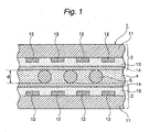
- Fig. 1 is a schematic sectional view of a liquid crystal display cell of the present invention.
- a pair of substrates with transparent electrode film at least one of which has a transparent electrode film, a transparent film and an alignment layer laminated successively on a surface of a substrate, are arranged at a given distance in such a manner that the transparent electrode films face each other, and in a gap formed between the pair of substrates with transparent electrode film, a liquid crystal is enclosed.
- the substrate is not specifically restricted.
- the substrates include a glass substrate, a ceramic substrate, a metal substrate and a plastic substrate.
- the substrate is appropriately selected therefrom according to the purpose.
- One of the substrates has only to be transparent, so that two substrates made of different materials may be used as a pair.
- Fig. 1 is a schematic sectional view of an embodiment of the liquid crystal display cell of the invention.
- the liquid crystal display cell 1 is formed by arranging a pair of substrates with transparent electrode film 2, 2, in each of which a transparent electrode film 12, a transparent film 13 and an alignment layer 14 are laminated successively on a surface of a glass substrate 11, at a given distance d in such a manner that the transparent electrode films 12, 12 face each other and enclosing a liquid crystal 4 in a gap formed between the pair of substrates with transparent electrode film 2, 2. Between the substrates with transparent electrode film 2, 2, plural spacers 5 may be interposed to make the given distance d.
- the transparent film 13 is a film formed by applying a transparent film-forming coating solution described later onto the substrate having been provided with the transparent electrode film 12 and then drying the coated layer.
- the transparent film 13 has an extremely smooth surface, high surface hardness, excellent transparency, excellent mar resistance, high insulation resistance and good adhesion to the alignment layer, and can effectively decrease the amount of mobil ions in the liquid crystal panel.
- a substrate with transparent electrode film further having an alkali passivation film, such as a SiO 2 film, between the glass substrate 11 and the transparent electrode film 12 may be used in the liquid crystal display cell of the invention.
- the "average surface roughness" referred to herein with regard to the surface smoothness of the transparent electrode film, the transparent film and the alignment layer is in accordance with JIS B 0601-1982 and is expressed as a value of two times the center line average roughness (Ra), i.e., a value of 2(Ra).
- the surface irregularities and the heights thereof are measured by an atomic force microscope (AFM) (manufactured by Seiko Denshi Kogyo K.K., SPI3700).
- the transparent electrode film 12 formed on the surface of the glass substrate a conventional transparent electrode film is employable, and examples thereof include films of conductive oxides such as ITO and films of metals such as gold and silver.
- the average surface roughness of the transparent electrode film is not specifically restricted, it is preferably not more than 30 nm, more preferably not more than 10 nm. If the average surface roughness exceeds 30 nm, the finally obtained alignment layer (formed on the transparent film) does not have an average surface roughness of not more than 7 nm in some cases, and when a ferroelectric liquid crystal is used, structural defect is sometimes brought about to thereby lower display ability.
- the transparent electrode film can be produced by a conventional method such as a CVD method or a coating method.
- the thickness of the transparent electrode film has only to be such a thickness as is capable of retaining conduction and is not detrimental to the transparency.
- the transparent film is formed on the transparent electrode film, comprises a matrix component (A) and ion-adsorbing inorganic oxide fine particles (B) and functions as an insulating film.
- the thickness of the transparent film is in the range of preferably 10 to 500 nm, more preferably 30 to 200 nm.
- the thickness of the transparent film is less than the lower limit of the above range, pinhole defect is liable to occur in the transparent film, and shedding of transparent film is liable to occur on the transparent film. Thereby, uncoated portions tend to be produced. As a result, the transparent film neither functions as an insulating film nor has a uniform surface roughness.
- the thickness of the transparent film exceeds the upper limit of the above range, voltage loss attributable to the transparent film is increased in the driving of the liquid crystal panel by application of a voltage, and hence power consumption of the liquid crystal panel is increased to thereby lower serviceability.
- the transparent film desirably has pores having a pore volume of 0.01 to 0.3 ml/g, preferably 0.05 to 0.2 ml/g, and an average pore diameter of 1 to 10 nm, preferably 2 to 8 nm.
- pore volume is less than 0.01 ml/g, ion adsorption ability of the inorganic oxide fine particles is not sufficiently exhibited because of too few pores. If the pore volume exceeds 0.3 ml/g, strength of the film becomes insufficient.
- the average pore diameter is less than 1 nm, ion diffusion rate is slow when a voltage is applied, and ion adsorption ability of the ion-adsorbing inorganic oxide fine particles is not sufficiently exhibited in some cases. If the average pore diameter exceeds 10 nm, strength of the film becomes insufficient, and the average surface roughness of the transparent film sometimes exceeds 10 nm.
- the pore volume and the average pore diameter of the transparent film are determined by peeling a transparent film formed on a substrate and measuring a pore volume and an average pore diameter of the peeled transparent film by a N 2 adsorption method.
- the matrix component (A) to constitute the transparent film is desirably derived from at least one matrix-forming component selected from (a) an acetylacetonato chelate compound, (b) an organosilicon compound, (c) polysilazane and (d) metal alkoxide.
- the acetylacetonato chelate compound (a) has excellent film-forming properties, and besides, when a matrix component derived from the acetylacetonato chelate compound (a) is used, a transparent film having excellent alkali resistance, acid resistance, salt water resistance, water resistance and solvent resistance can be formed.
- a transparent film containing a matrix component derived from the organosilicon compound (b) is excellent in mar resistance, acid resistance, alkali resistance, water resistance and insulation properties.
- a transparent film containing a matrix component derived from the polysilazane (c) is almost free from cracks.
- a transparent film containing a matrix component derived from the metal alkoxide (d) is excellent in mar resistance, acid resistance, alkali resistance, water resistance and insulation properties.
- the weight ratio between the components is preferably as follows. That is to say, when the components derived from the acetylacetonato chelate compound (a), the organosilicon compound (b), the polysilazane (c) and the metal alkoxide (d) in the matrix component are each converted to an oxide or a nitride, the weight ratio between the components preferably satisfies the following relation.
- the component derived from the acetylacetonato chelate compound especially is contained and the above weight ratio is not less than 0.001, a film having excellent alkali resistance, acid resistance, salt water resistance, water resistance and solvent resistance can be obtained.
- the compounding ratio between the component derived from the organosilicon compound, the component derived from the polysilazane and the component derived from the metal alkoxide preferably satisfies the relation 0 ⁇ M 2 O x /(SiO 2 +SiN+M 2 O x ) ⁇ 1.0.
- the ion-adsorbing inorganic oxide fine particles (B) have an average particle diameter of 1 nm to 50 nm, preferably 2 nm to 40 nm.
- the transparent film having a thickness of 10 to 500 nm formed on the transparent electrode film has good reproducibility and has an average surface roughness of not more than 10 nm in spite of the surface roughness of the transparent electrode film.
- the transparent film exhibits excellent adhesion to a hydrophobic alignment layer, and on the transparent film, a smooth alignment layer having an average surface roughness of not more than 7 nm, preferably not more than 3 nm, can be formed with good reproducibility.
- the average particle diameter of the inorganic oxide fine particles can be measured by a laser Doppler method or TEM observation.
- Examples of the ion-adsorbing inorganic oxide fine particles (B) include fine particles of inorganic oxides, such as SiO 2 , Al 2 O 3 , ZrO 2 , TiO 2 , SnO 2 , In 2 O 3 and Sb 2 O 5 , and fine particles of composite inorganic oxides, such as SiO 2 ⁇ Al 2 O 3 , SiO 2 ⁇ TiO 2 , In 2 O 3 ⁇ SnO 2 , Sb 2 O 5 ⁇ SnO 2 and SnO 2 ⁇ In 2 O 3 ⁇ Sb 2 O 5 or solid solutions thereof. Also employable are mixtures of two or more kinds of these oxides.
- the ion-adsorbing inorganic oxide fine particles are those having water of crystallization (may be hydroxyl group). More specifically, preferable are inorganic metal oxide fine particles which have a number n of moles of water of 0.02 to 5 when the inorganic oxide is represented by MO x ⁇ nH 2 O and when the water of crystallization other than water of adhesion, the structural hydroxyl group and the surface hydroxyl group are converted to H 2 O.
- the number n of moles of water is preferably in the range of 0.1 to 5.
- n of moles of water such as water of crystallization in the ion-adsorbing inorganic oxide fine particles is less than 0.02, ion adsorption capability is too small and ions in the liquid crystal cannot be adsorbed effectively. It is difficult to obtain ion-adsorbing inorganic oxide fine particles having a number of moles of more than 5. Even if such particles are obtained, water molecules are sometimes eliminated from the inorganic oxide fine particles to inhibit alignment of the liquid crystal.
- the number n of moles of water in the ion-adsorbing inorganic oxide fine particles can be determined as follows.
- the ion-adsorbing inorganic oxide fine particles are dried at 120°C until a constant weight is reached, then the ion-adsorbing inorganic oxide fine particles are subjected to differential thermal analysis, and the amount of water decreased by the time the temperature becomes 500°C is calculated as a number of moles of water based on 1 mol of the total of the inorganic metal oxides.
- the ion-adsorbing inorganic oxide fine particles (B) are preferably fine particles capable of adsorbing inorganic and/or organic ions present as impurities in the liquid crystal or eluted into the liquid crystal from the alignment layer or a sealing material, and these fine particles preferably have an ion adsorption capability of 0.1 to 3.0 mmol/g.
- ion adsorption capability is less than the lower limit of the above range, decrease of the amount of mobil ions is insufficient, and hence voltage retention properties are lowered and reliability is lowered. In addition, display failures take place or power consumption cannot be reduced in some cases.
- inorganic oxide fine particles (B) having an ion adsorption capability of higher than the upper limit of the above range.
- Examples of ions capable of being adsorbed by the ion-adsorbing inorganic oxide fine particles (B) include inorganic cations, such as Na + , K + , Rb + , Cs + , Li + , Ag + , Mg 2+ , Ca 2+ , Sr + , Ba 2+ and NH 4 + , inorganic anions, such as F - , Cl - and SO 4 2- , organic anions, such as formic acid ion and acetic acid ion, and organic cations, such as tetraethylammonium ion and tetrapropylammonium ion.
- inorganic cations such as Na + , K + , Rb + , Cs + , Li + , Ag + , Mg 2+ , Ca 2+ , Sr + , Ba 2+ and NH 4 +
- inorganic anions such as F - , Cl - and SO 4 2-
- the ion adsorption capability of the ion-adsorbing inorganic oxide fine particles is measured in the following manner.
- a NaCl aqueous solution having a concentration of 1% by weight 1.5 g of ion-adsorbing inorganic oxide fine particles having been dried to constant weight at 120°C are added, and they are stirred at room temperature (25°C) for 15 hours. Thereafter, the mixture is filtered to obtain a filtrate. Then, a Na ion concentration of the filtrate is analyzed by atomic absorption spectrometry, and from a difference in the Na ion concentration between the filtrate and the original NaCl aqueous solution, inorganic cation adsorption capability (mmol/g) of the ion-adsorbing inorganic oxide fine particles is determined.
- a tatermethylammonium hydroxide aqueous solution having a concentration of 1% by weight 1.5 g of ion-adsorbing inorganic oxide fine particles having been dried to constant weight at 120°C are added, and they are stirred at room temperature (25°C) for 15 hours. Thereafter, the mixture is filtered to obtain a filtrate. Then, a tetramethylammonium ion concentration of the filtrate is analyzed by ion chromatography, and from a difference in the concentration between the filtrate and the original aqueous solution, organic cation adsorption capability (mmol/g) of the ion-adsorbing inorganic oxide fine particles is determined.
- acetic acid aqueous solution having a concentration of 1% by weight
- 1.5 g of ion-adsorbing inorganic oxide fine particles having been dried to constant weight at 120°C are added, and they are stirred at room temperature (25°C) for 15 hours. Thereafter, the mixture is filtered to obtain a filtrate. Then, an acetic acid ion concentration of the filtrate is analyzed by ion chromatography, and from a difference in the concentration between the filtrate and the original aqueous solution, organic anion adsorption capability (mmol/g) of the ion-adsorbing inorganic oxide fine particles is determined.
- insulating or conductive inorganic compound particles may be used in combination, when needed.
- the conductive inorganic oxide fine particles are used preferably in a state of a sol wherein these particles are dispersed in water or an organic solvent, conductive inorganic oxide fine particles in a state other than the sol state may be used provided that they can be monodispersed or nearly monodispersed in the transparent film-forming coating solution.
- the content of the matrix component (A) in the transparent film is preferably in the range of 30 to 35% by weight in terms of an oxide or a nitride, and the content of the ion-adsorbing inorganic oxide fine particles is preferably in the range of 5 to 70% by weight in terms of an oxide.
- the matrix component and the ion-adsorbing inorganic oxide fine particles are present in the above amounts in the transparent film, even an alignment layer composed of a highly hydrophobic resin such as a polyimide resin can be formed on the surface of the transparent film with good adhesion to the transparent film.
- the transparent film can effectively decrease the amount of ions in the liquid crystal panel.
- the surface roughness of the transparent electrode film is not more than 30 nm
- a smooth transparent film having an average surface roughness of not more than 10 nm can be formed, and on such a transparence film, an alignment layer composed of a highly hydrophobic resin such as a polyimide resin can be formed with good adhesion to the transparent film.
- the alignment layer formed on the surface of the transparent film has a smooth surface having an average surface roughness of not more than 7 nm, causes no structural defect and can favorably orientate the liquid crystal. Therefore, a liquid crystal display cell having high-speed response, wide angle of view, bistable memory properties, high contrast, large-screen display ability, etc. can be obtained.
- the alignment layer and the material or eluted therefrom can be adsorbed, so that the liquid crystal can be made substantially free from ions.
- the operating voltage can be lowered, the voltage retention can be increased, and the power consumption can be reduced.
- a smooth transparent film having an average surface roughness of not more than 10 nm can be formed, and on such a transparence film, an alignment layer composed of a highly hydrophobic resin such as a polyimide resin can be formed with good adhesion to the transparent film. Further, a smooth alignment layer having an average surface roughness of not more than 7 nm, causing no structural defect and favorably orientating the liquid crystal can be obtained.
- the average surface roughness referred to herein is expressed as a value of two times the center line average roughness (Ra) in JIS B 0601-1982.
- the process for forming the transparent film is not specifically restricted, and for example, the transparent film can be formed by applying and drying (and calcining when necessary) the below-described transparent film-forming coating solution.
- the transparent film-forming coating solution for use in the invention is a solution wherein a matrix component precursor (A') and the ion adsorbing inorganic oxide fine particles are dispersed in a mixed solvent of water and an organic solvent.
- matrix component precursor (A') a compound selected from an acetylacetonato chelate compound, an organosilicon compound, polysilazane and metal alkoxide or a mixture of two or more compounds selected therefrom is employed.
- the acetylacetonato chelate compound is a chelate compound having acetylacetone as a ligand and is a compound represented by the following chemical formula (1) or its condensate.
- a+b is a number of 2 to 4
- a is a number of 0 to 3
- b is a number of 1 to 4
- X is -CH 3 , -OCH 3 , -C 2 H 5 or -OC 2 H 5
- M 1 is an element selected from Group IB, Group IIA, Group IIB, Group IIIA, Group IIIB, Group IVA, Group IVB, Group VA, Group VB, Group VIA, Group VIIA and Group VIII, or vanadyl (VO).
- acetylacetonato chelate compounds include dibutoxy-bisacetylacetonatozirconium, tributoxy-monoacetylacetonatozirconium, bisacetylacetonatolead, trisacetylacetonatoiron, dibutoxy-bisacetylacetonatohafnium and monoacetylacetonatotributoxyhafnium.
- organisilicon compound an organosilicon compound represented by the following formula is employed.
- R a -Si(OR') 4-a wherein R is -C n H 2n+1 , R' is -C n H 2n+1 or -C 2 H 4 OC n H 2n+1 , a is an integer of 0 to 3, and n is an integer of 1 to 4.
- organosilicon compounds include tetramethoxysilane, tetraethoxysilane, monomethyltrimethoxysilane, monoethyltriethoxysilane, monoethyltrimethoxysilane and monomethyltriethoxysilane.
- organosilicon compounds may be used as they are or after partially hydrolyzed.
- the partial hydrolyzates can be obtained in accordance with usual methods heretofore used, for example, a method comprising mixing the organosilicon compound with an alcohol such as methanol or ethanol and adding water and an acid to the mixture to perform partial hydrolysis.
- a film having excellent mar resistance, acid resistance, alkali resistance, water resistance and insulation properties can be formed, and besides the surface of an alignment layer subsequently formed thereon can be made extremely smooth.
- M 2 in the above formula is not specifically restricted provided that it is a metal, but M 2 is preferably Be, Al, Sc, Ti, V, Cr, Fe, Ni, Zn, Ga, Ge, As, Se, Y, Zr, Nb, In, Sn, Sb, Te, Hf, Ta, W, Pb, Bi, Ce or Cu.
- metal oxides preferably used include tetrabutoxyzirconium, diisopropoxy-dioctyloxytitanium and diethoxylead.
- the transparent film-forming coating solution containing the metal alkoxide When the transparent film-forming coating solution containing the metal alkoxide is applied, then dried and calcined, the metal alkoxide is polymerization cured, whereby a film having excellent mar resistance, acid resistance, alkali resistance and insulation properties can be formed.
- polysilazane having a recurring unit represented by the following formula (3) is employed as the polysilizane.
- R 1 , R 2 and R 3 are each a hydrogen atom or an alkyl group of 1 to 8 carbon atoms.
- polysilazane having a recurring unit represented by the formula (3) is used as the matrix component precursor
- polysilazane having a methyl group, an ethyl group or a propyl group as the alkyl group is preferable.
- there is no alkyl group to be decomposed in the heating process and film shrinkage is little in the heating process. Therefore, cracks are hardly produced when shrinkage stress is applied to the film, and a transparent film almost free from cracks and having excellent surface smoothness can be obtained.
- the polysilazane having a recurring unit represented by the formula (3) may be straight-chain or cyclic, or may be a mixture of straight-chain polysilanzane and cyclic polysilazane.
- the polysilazane desirably has a number-average molecular weight of 500 to 10,000, preferably 1,000 to 4,000. If the number-average molecular weight is less than 500, low-molecular weight polysilazane evaporates in the heat curing process, and the resulting transparent film tends to be porous. If the number-average molecular weight exceeds 10,000, flowability of the coating solution tends to be lowered, and hence surface smoothness of the transparent film tends to be lowered.
- the matrix component precursors mentioned above may be used singly or in combination of two or more kinds.
- the matrix component precursor (A') and the ion-adsorbing inorganic oxide fine particles (B) are dispersed in a mixed solvent of water and an organic solvent.
- organic solvents used for the transparent film-forming coating solution include conventional organic solvents, such as alcohols, ethers, glycols and ketones. Such organic solvents may be used singly or in combination of two or more kinds.
- the solids concentration of the coating solution is preferably not more than 15% by weight as a total value of the matrix component precursor (A') and the ion-adsorbing inorganic oxide fine particles (B) in terms of an oxide or a nitride.
- solids concentration exceeds 15% by weight, storage stability of the coating solution tends to be lowered. If the solids concentration is extremely low, it is necessary to carry out coating operations many times in order to obtain the aimed film thickness. Therefore, a solids concentration of not less than 0.1% by weight is practical.
- the matrix component precursor (A') is preferably contained in such an amount that the amount of the matrix component in the resulting transparent film becomes 30 to 95% by weight in terms of an oxide or a nitride.
- the ion-adsorbing inorganic oxide fine particles (B) are preferably contained in such an amount that the amount of the ion-adsorbing inorganic oxide fine particles in the resulting transparent film becomes 5 to 70% by weight.
- the ion-adsorbing inorganic oxide fine particles are present in the above amount in the transparent film-forming coating solution, even an alignment layer composed of a highly hydrophobic resin such as a polyimide resin can be formed on a surface of a transparent film obtained from the coating solution with good adhesion to the transparent film. Further, a transparent film capable of effectively decreasing the amount of ions in the liquid crystal panel can be formed. If the amount of the ion-adsorbing inorganic oxide fine particles exceeds 70% by weight, adhesion between the transparent film and the transparent electrode film is lowered or the transparent film does not have an average surface roughness of not more than 10 nm in some cases.
- the ion-adsorbing inorganic oxide fine particles and the fine particles other than the ion-adsorbing inorganic oxide fine particles are preferably present in the coating solution in such amounts that the total amount of these fine particles in the resulting transparent film becomes 5 to 70% by weight in terms of an oxide or a nitride.
- the water concentration of the coating solution is preferably in the range of 0.1 to 50% by weight. If the water concentration is less than 0.1% by weight, hydrolysis, condensation polymerization and complexing (adherence) of the acetylacetonato chelate compound, the organosilicon compound, the polysilazane and the metal alkoxide cannot be carried out sufficiently, and mar resistance and durability of the resulting film tend to be lowered. If the water concentration exceeds 50% by weight, the coating solution is liable to be repelled by the substrate in the coating process, and film formation becomes difficult.
- the mixing ratio between the matrix component precursor (A') and the ion-adsorbing inorganic oxide fine particles (B), the type of the metal contained in the matrix component precursor (A'), the type of the ion-adsorbing inorganic oxide fine particles (B) contained in the coating solution, refractive index and dielectric constant of the resulting film can be freely controlled.
- the refractive index of the transparent film becomes higher than that of the alignment layer to be formed thereon, the electrode from cannot be seen through the alignment layer.
- the transparent film can be formed by a process comprising applying the transparent film-forming coating solution onto a surface of a substrate, such as a glass substrate having a transparent electrode film, by dipping, spinner method, spraying, roll coating, flexographic printing or the like and then drying the coated layer at a temperature of room temperature to 90°C, heating the dried layer to a temperature of not lower than 200°C, occasionally not lower than 300°C, to cure the layer.
- a substrate such as a glass substrate having a transparent electrode film
- dipping, spinner method, spraying, roll coating, flexographic printing or the like then drying the coated layer at a temperature of room temperature to 90°C, heating the dried layer to a temperature of not lower than 200°C, occasionally not lower than 300°C, to cure the layer.
- the transparent film formed on the substrate may be a film having been subjected to curing acceleration treatment in the following manner.
- the curing acceleration treatment is, for example, a treatment of irradiating the uncured film with electromagnetic wave of shorter wavelength than that of visible light after coating or after drying or during drying, or a treatment of exposing the uncured film to an atmosphere of a gas that accelerates curing reaction.
- Examples of the electromagnetic waves used for the irradiation of the uncured film before heating include ultraviolet rays, electron rays, X rays and y rays. Of these, ultraviolet rays are particularly preferable.
- the film with ultraviolet rays having an energy quantity of not less than 100 mJ/cm 2 , preferably not less than 1000 mJ/cm 2 , using, for example, a high-pressure mercury lamp having the maximum emission intensity at about 250 nm and 360 nm and having a light intensity of not less than 10 mW/cm 2 as a source of ultraviolet rays.
- Examples of the gases used for accelerating curing reaction of the uncured film before heating include ammonia and ozone.
- the gas treatment it is desirable to expose the uncured film to the active gas atmosphere having a gas concentration of 100 to 100,000 ppm, preferably 1,000 to 10,000 ppm.
- the gas treatment may be carried out after heat curing, and also in this case, the same effect can be obtained.
- the alignment layer used in the liquid crystal display cell of the invention has an average surface roughness of not more than 7 nm, preferably not more than 3 nm. If the average surface roughness of the alignment layer exceeds 7 nm, alignment of the liquid crystal becomes nonuniform, and structural defect (zigzag defect) sometimes occurs to cause a problem of lowering of display ability.
- the alignment layer for use in the invention is preferably an alignment layer composed of a polyimide resin. From the polyimide resin, an alignment layer having a small average surface roughness and excellent smoothness tends to be obtained.
- a polyimide resin SE-150, RN1199 available from Nissan Chemical industries, Ltd., RIXON ARIGHNER PIA-2910 available from Chisso Corporation, or the like is recommended.
- the alignment layer is formed on the transparent film having an average surface roughness of not more than 10 nm.
- the average surface roughness of the alignment layer is not more than 7 nm, no structural defect (zigzag defect) occurs even when a ferroelectric liquid crystal or an antiferroelectric liquid crystal is used, and a liquid crystal display cell having high-speed response, wide angle of view, bistable memory properties, high contrast and large-screen display ability can be obtained.
- the alignment layer can be formed by a heretofore known process comprising applying, for example, an alignment layer-forming resin coating material described below by flexographic printing, dipping, spin coating, spraying, roll coating or the like, then drying and heating.
- spin coating and flexographic printing are preferable because an alignment layer having a small average surface roughness and excellent smoothness tends to be obtained.
- the alignment layer-forming resin coating material a solution in which a precursor of the aforesaid polyimide resin, such as polyamic acid, is optionally dispersed or dissolved in an organic solvent such as dimethylacetamide is also employable.
- a solution in which a precursor of the aforesaid polyimide resin, such as polyamic acid, is optionally dispersed or dissolved in an organic solvent such as dimethylacetamide is also employable.
- an alignment layer having a small average surface roughness and excellent smoothness tends to be obtained. In this case, it is necessary to finally heat treating the film to perform polyimidation.
- liquid crystal used in the liquid crystal display cell of the invention a ferroelectric liquid crystal or an antiferroelectric liquid crystal is preferable.
- directions of dipoles namely, directions of liquid crystal molecules can be instantaneously switched by the positive or negative polarity of a voltage, differently from a nematic liquid crystal which depends upon change of molecular arrangement, and the above-mentioned liquid crystals have high-speed response, memory properties and bistability.
- a smectic liquid crystal particularly a chiral smectic liquid crystal
- examples thereof include chiral smectic C phase (SmC*), chiral smectic H phase (SmH*), chiral smectic I phase (SmI*), chiral smectic J phase (SmJ*), chiral smectic K phase (SmK*), chiral smectic G phase (SmG*) and chiral smectic F phase (SmF*).
- SmC* chiral smectic C phase
- SmH* chiral smectic H phase
- I* chiral smectic I phase
- SmJ* chiral smectic J phase
- SmK* chiral smectic K phase
- SmG* chiral smectic G phase
- SmF* chiral smectic F phase
- the absolute value of spontaneous polarization of the liquid crystal molecule is in the range of preferably 2 to 500 nC/cm 2 , more preferably 3 to 200 nC/cm 2 .
- the response speed becomes insufficient though it depends upon working temperature and viscosity of the liquid crystal.
- ferroelectric liquid crystals examples are given below.
- Liquid crystals derived from the above-mentioned liquid crystals are also preferably employed.
- the ferroelectric liquid crystal for use in the invention is also employable for a ferroelectric liquid crystal cell showing V-shaped switching properties (transmittance becomes symmetric to the polarity of a voltage applied for driving) or anti-V-shaped switching properties (transmittance does not become symmetric to the polarity of a voltage applied for driving), when necessary.
- a polymer stabilizer may be contained together with the liquid crystal.
- a high-molecular resin is employed.
- a liquid crystal layer showing the V-shaped switching properties or the anti-V-shaped switching properties can be easily formed.
- the compounding ratio between the liquid crystal and the polymer stabilizer varies depending upon the type of the liquid crystal used, it is desired that the amount of the polymer stabilizer is in the range of 1 to 30% by weight, preferably 2 to 10% by weight, based on the total amount of the liquid crystal and the polymer stabilizer.
- the amount of the polymer stabilizer is less than 1% by weight, the liquid crystal layer cannot be stably held in, for example, a SmC* phase occasionally though it depends upon the type of the liquid crystal used, and even when irradiated with ultraviolet rays, a ferroelectric liquid crystal cell showing the V-shaped switching properties or the anti-V-shaped switching properties cannot be obtained in some cases. If the amount of the polymer stabilizer exceeds 30% by weight, response time, angle of view, bistable memory properties and contrast tend to be lowered because the amount of the polymer stabilizer is too large.
- an organic resin is employed as the polymer stabilizer. Above all, a photo-functional resin is preferable, and an ultraviolet or electron ray curing monovalent or polyvalent acrylate or methacrylate monomer or a mixture thereof is particularly preferable.
- Examples of such resins include 1,6-hexanediol acrylate, 2-(2-ethoxyethoxy)ethyl acrylate, stearyl acrylate, 1,3-butanediol acrylate, cyclohexyl methacrylate and indecyl methacrylate.
- the liquid crystal layer containing the polymer stabilizer can be obtained by blending the ultraviolet curing resin monomer with a liquid crystal, enclosing the blend between the substrates with transparent electrode film, applying a voltage to hold the liquid crystal layer in a defect-free state such as the aforesaid SmC*, SmH* or SmI* phase and irradiating the liquid crystal layer with ultraviolet rays to cure the ultraviolet curing resin monomer.
- the liquid crystal display cell having the thus obtained liquid crystal layer containing the polymer stabilizer, a defect-free state of the liquid crystal layer can be easily formed, and such a state can be stably maintained.
- the liquid crystal display cell has high-speed response, wide angle of view, bistable memory properties and high contrast.
- spacers can be interposed between the transparent electrode films arranged so as to face each other and/or near the peripheries thereof.
- spacers heretofore known spacers are employable, and for example, inorganic oxide particles such as particles of silica and alumina, organic-inorganic composite particles such as polyorganosiloxane particles, or organic resin particles are employable.
- the average particle diameter of the spacers is preferably smaller than a helical pitch of the liquid crystal used, and it is in the range of usually 0.5 to 10 ⁇ m, preferably 1 to 5 ⁇ m.
- the helical structure of the liquid crystal is dissolved to arrange the liquid crystal molecules in one direction.
- the directions of dipoles namely, directions of the liquid crystal molecules can be switched by the positive or negative polarity of the voltage.
- the aforesaid ferroelectric liquid crystal or antiferroelectric liquid crystal is used as the liquid crystal, a liquid crystal display cell having a switching time extremely faster than that of the nematic liquid crystal cell and having high-speed response of the order of microsecond can be obtained.
- liquid crystal display cell having memory properties such that the arrangement state of the liquid crystal molecules is maintained even after application of a voltage is stopped and having bistability such that the directions of the liquid crystal molecules can be in two stable states can be obtained.
- the liquid crystal display cell of the invention can be prepared in the following manner.
- a transparent electrode film is formed on the surface of a glass substrate, then a transparent film is formed on the surface of the transparent electrode film, and an alignment layer is further formed on the surface of the transparent film, as described above.
- the alignment layer is subjected to rubbing treatment once in one direction so that the rubbing directions should become parallel.
- a pair of substrates with transparent electrode film are obtained.
- a sealing material is printed, and if necessary, spacer particles are scattered.
- the substrates are bonded in such a manner that the transparent electrode films face each other.
- a liquid crystal and if necessary a polymer stabilizer are poured, and the pour opening is sealed with a sealing material.
- sealing materials include thermosetting resins such as epoxy resin and phenolic resin.
- the spacer particles may be contained, as previously described.
- the transparent film to constitute the liquid crystal display cell of the invention contains ion-adsorbing inorganic oxide particles having particle diameters of a specific range, and hence the surface of the transparent film formed on the transparent electrode film has excellent smoothness and has excellent adhesion to the hydrophobic alignment layer formed on the transparent film. Further, also the surface of the alignment layer formed on the transparent film is extremely smooth, and hence orientation properties of the liquid crystal are excellent.
- the liquid crystal is formed by the use of a polymer stabilizer, and therefore structural defect does not occur for a long period of time. Accordingly, by the use of the liquid crystal display cell of the invention, a display device having high-speed response, bistable memory properties and excellent impact resistance can be obtained.
- the transparent film used in the invention contains inorganic oxide particles having inorganic ion adsorption ability, mobil ions in the liquid crystal layer can be adsorbed and decreased.
- the liquid crystal display cell of the invention needs only low operating voltage and has excellent voltage retention properties. Accordingly, the liquid crystal display cell of the invention can reduce power consumption and has excellent display ability.
- ethyl silicate28 SiO 2 concentration: 28% by weight
- 40 g of butyl cellosolve, 304.4 g of hexylene glycol, 0.4 g of nitric acid having a concentration of 61% by weight and 15 g of pure water were added, and they were stirred at room temperature for 2 hours.
- 15 g of an amphoteric ion-exchange resin available from Mitsubishi Chemical Corporation, Diaion
- the amphoteric ion-exchange resin was removed to obtain a dispersion of a partial hydrolyzate (oligomer) of ethyl silicate.
- an inorganic ion-adsorbing fine particle sol having a solids concentration of 10% by weight obtained by homogeneously dispersing antimony pentoxide fine particles (Sb 2 O 5 ⁇ 2.7H 2 O, ion adsorption capability: 2.4 mmol/g) having an average particle diameter of 20 nm as inorganic oxide fine particles in hexylene glycol was added, and they were stirred for 30 minutes.
- a glass substrate having a patterned ITO display electrode (available from Asahi Glass Co., Ltd., product of not more than 30 ⁇ / ⁇ , average surface roughness: 26.6 nm) was coated with the transparent film-forming coating solution (A) by flexographic printing.
- the coated layer was dried at 90°C for 5 minutes, then irradiated with ultraviolet rays by means of a high-pressure mercury lamp under the conditions of integral light quantity of 6,000 mJ/cm 2 (measured by a sensor for 365 nm) and then calcined at 300°C for 30 minutes to form a transparent film (A).
- Measurement of a thickness of the transparent film (A) by a direct contact type surface roughness meter resulted in 70 nm.
- An average surface roughness of the transparent film is set forth in Table 2.
- the transparent film (A) was coated with a polyimide film-forming coating material (available from Nissan Chemical Industries, Ltd., RN1199) by flexographic printing.
- the coated layer was dried at 100°C for 5 minutes and then heated at 240°C for 30 minutes to form an alignment layer (polyimide film).
- An average surface roughness of the alignment layer and the following adhesion properties were measured. The results are set forth in Table 2.
- the alignment layer was subjected to rubbing treatment once in one direction so that the rubbing directions on the upper and the lower substrates should become parallel, whereby one pair of substrates with transparent electrode film in each of which the transparent electrode film, the transparent film (A) and the alignment layer having been subjected to rubbing treatment were laminated successively on the glass substrate were obtained.
- a sealing material composed of an epoxy resin and silica fine particles (available from Catalysts & Chemicals Industries Co., Ltd., SW-D1, average particle diameter: 1.8 ⁇ m) was printed, and these substrates were bonded in such a manner that the transparent electrode films faced each other, followed by pouring a ferroelectric liquid crystal (available from Clariant Japan, FELIX M4851/100, response time: 38 ⁇ s, tilt angle:30.5° (room temperature)). Then, the pour opening was sealed with a sealing material to prepare a liquid crystal display cell (A) having a liquid crystal layer thickness of 2 ⁇ m.
- the resulting liquid crystal display cell (A) was evaluated on the mobil ion quantity, display nonuniformity, presence of structural defect and impact resistance in the following manner.
- the mobil ion quantity in the resulting liquid crystal display cell (A) was measured by an ion density measuring machine (available from Toyo Technica, MTR-1) under the conditions of an applied voltage of 10 V and a triangular wave frequency of 0.1 Hz.
- the liquid crystal display cell in which any structural defect had not been observed at all was given an impact in a drop test of dropping the cell from the height of 10 cm, and presence of structural defect was observed in the same manner as described above.
- Formation of a transparent film (A) was carried out on each of 10 substrates, and an average surface roughness of the resulting each transparent film was measured.
- the mean of the average surface roughness values of the 10 transparent films was 6.9 nm, the maximum value was 7.3 nm, and the minimum value was 6.8 nm.
- an alignment layer (A) was formed on each transparent film (A), and an average surface roughness of each of the 10 alignment layers was measured.
- the mean of the average surface roughness values of the 10 alignment layers was 2.2 nm, the maximum value was 2.3 nm, and the minimum value was 2.1 nm.
- a transparent film-forming coating solution (B) was prepared in the same manner as in Example 1, except that silica alumina fine particles (0.75SiO 2 ⁇ 0.25Al 2 O 3 ⁇ 0.3H 2 O) having an average particle diameter of 25 nm and ion adsorption capability of 0.5 mmol/g obtained by drying silica alumina (available from Catalysts & Chemicals Industries Co., Ltd., USB sol) were used as the inorganic oxide fine particles. Then, a transparent film and an alignment layer were formed in the same manner as in Example 1. Then, an average surface roughness and adhesion properties of the alignment layer were measured in the same manner as in Example 1.
- liquid crystal display cell (B) was prepared in the same manner as in Example 1.
- the resulting liquid crystal display cell (B) was evaluated on the mobil ion quantity, presence of structural defect and impact resistance.
- a ferroelectric liquid crystal (available from Clariant Japan, FELIX M4851/100, response time: 38 ⁇ s, tilt angle: 30.5° (room temperature)).
- an acrylate monomer UCL-003 available from Dainippon Ink & Chemicals Inc.
- the liquid crystal layer was irradiated with ultraviolet rays (UV wavelength: 365 nm, irradiation intensity: 2 mW/cm 2 ) for 240 seconds with application of a voltage to the liquid crystal cell, to prepare a liquid crystal display cell (C) having a liquid crystal layer thickness of 2 ⁇ m.
- the resulting liquid crystal display cell (C) was evaluated on the mobil ion quantity, presence of structural defect and impact resistance.
- ethyl silicate28 SiO 2 concentration: 28% by weight
- 40 g of butyl cellosolve, 304.4 g of hexylene glycol, 0.4 g of nitric acid having a concentration of 61% by weight and 15 g of pure water were added, and they were stirred at room temperature for 2 hours.
- 15 g of an amphoteric ion-exchange resin available from Mitsubishi Chemical Corporation, Diaion
- the amphoteric ion-exchange resin was removed to obtain a dispersion of a partial hydrolyzate (oligomer) of ethyl silicate.
- TiO 2 concentration diisopropoxy-dioctyloxytitanium
- ZrO 2 concentration tributoxy-monoacetylacetonatozirconium
- a liquid crystal display cell (D) was prepared in the same manner as in Example 1, except that the transparent film-forming coating solution (B) was used.
- the resulting liquid crystal display cell (D) was evaluated on the mobil ion quantity, presence of structural defect and impact resistance.
- Formation of a transparent film (E) was carried out on each of 10 substrates, and an average surface roughness of the resulting each transparent film was measured.
- the mean of the average surface roughness values of the 10 transparent films was 12.5 nm, the maximum value was 15.3 nm, and the minimum value was 11.8 nm.
- an alignment layer (E) was formed on each transparent film (E), and an average surface roughness of each of the 10 alignment layers was measured.
- the mean of the average surface roughness values of the 10 alignment layers was 3.5 nm, the maximum value was 4.1 nm, and the minimum value was 2.9 nm.
- a transparent film-forming coating solution (C) was prepared in the same manner as in Example 1, except that silica particles (SiO 2 ⁇ 0.1H 2 O) having an average particle diameter of 80 nm obtained by drying Cataloid SI-80P (available from Catalysts & Chemicals Industries Co., Ltd.) were used.
- a liquid crystal display cell (E) was prepared in the same manner as in Example 1, except that the transparent film-forming coating solution (C) was used.
- the resulting liquid crystal display cell (E) was evaluated on the mobil ion quantity, presence of structural defect and impact resistance.
- a liquid crystal display cell (F) was prepared in the same manner as in Example 3, except that the transparent film was not formed.
- the resulting liquid crystal display cell (F) was evaluated on the mobil ion quantity, presence of structural defect and impact resistance.
Landscapes
- Physics & Mathematics (AREA)
- Nonlinear Science (AREA)
- Chemical & Material Sciences (AREA)
- Crystallography & Structural Chemistry (AREA)
- General Physics & Mathematics (AREA)
- Optics & Photonics (AREA)
- Mathematical Physics (AREA)
- Liquid Crystal (AREA)
Applications Claiming Priority (3)
| Application Number | Priority Date | Filing Date | Title |
|---|---|---|---|
| JP2001383662 | 2001-12-17 | ||
| JP2001383662A JP2003186054A (ja) | 2001-12-17 | 2001-12-17 | 液晶表示セル |
| PCT/JP2002/012916 WO2003052505A1 (fr) | 2001-12-17 | 2002-12-10 | Cellule d'affichage a cristaux liquides |
Publications (2)
| Publication Number | Publication Date |
|---|---|
| EP1465005A1 true EP1465005A1 (fr) | 2004-10-06 |
| EP1465005A4 EP1465005A4 (fr) | 2006-06-21 |
Family
ID=19187613
Family Applications (1)
| Application Number | Title | Priority Date | Filing Date |
|---|---|---|---|
| EP02788769A Withdrawn EP1465005A4 (fr) | 2001-12-17 | 2002-12-10 | Cellule d'affichage a cristaux liquides |
Country Status (7)
| Country | Link |
|---|---|
| US (1) | US20050046782A1 (fr) |
| EP (1) | EP1465005A4 (fr) |
| JP (1) | JP2003186054A (fr) |
| KR (1) | KR20040066913A (fr) |
| CN (1) | CN1605043A (fr) |
| TW (1) | TW200301393A (fr) |
| WO (1) | WO2003052505A1 (fr) |
Cited By (1)
| Publication number | Priority date | Publication date | Assignee | Title |
|---|---|---|---|---|
| WO2020016752A1 (fr) * | 2018-07-20 | 2020-01-23 | 3M Innovative Properties Company | Film optique comprenant un réflecteur optique polymère et un revêtement transparent discontinu |
Families Citing this family (12)
| Publication number | Priority date | Publication date | Assignee | Title |
|---|---|---|---|---|
| WO2006019032A1 (fr) * | 2004-08-17 | 2006-02-23 | Matsushita Electric Industrial Co., Ltd. | Écran plasma et son procédé de fabrication |
| TWI318235B (en) * | 2005-08-29 | 2009-12-11 | Univ Chung Yuan Christian | Liquid crystal composite material |
| TW200742610A (en) * | 2006-05-10 | 2007-11-16 | Tpk Touch Solutions Inc | Method of hiding transparent electrodes on a transparent substrate |
| JP4968262B2 (ja) * | 2006-12-20 | 2012-07-04 | 富士通株式会社 | 液晶表示素子及びそれを用いた電子ペーパー |
| CN103231568B (zh) * | 2007-04-13 | 2016-03-02 | 宇部兴产株式会社 | 一面平滑的聚酰亚胺薄膜 |
| FR2934380B1 (fr) * | 2008-07-25 | 2010-09-03 | Nemoptic | Procede de realisation de dispositifs a cristaux liquides nematiques bistables. |
| CN104098725B (zh) | 2014-06-05 | 2016-02-10 | 京东方科技集团股份有限公司 | 一种组合物、取向层及其制备方法、液晶取向单元、液晶显示面板 |
| US11300837B2 (en) * | 2016-06-07 | 2022-04-12 | Lg Chem, Ltd. | Method of applying particles |
| CN109976017B (zh) * | 2019-04-10 | 2021-09-24 | 深圳市华星光电半导体显示技术有限公司 | 显示面板及其制作方法 |
| US11502104B2 (en) | 2019-08-15 | 2022-11-15 | Sandisk Technologies Llc | Antiferroelectric memory devices and methods of making the same |
| US11430813B2 (en) | 2019-08-15 | 2022-08-30 | Sandisk Technologies Llc | Antiferroelectric memory devices and methods of making the same |
| CN114614244B (zh) * | 2020-12-04 | 2023-09-08 | 上海中航光电子有限公司 | 一种液晶天线及其制作方法 |
Family Cites Families (4)
| Publication number | Priority date | Publication date | Assignee | Title |
|---|---|---|---|---|
| JPH0836165A (ja) * | 1994-07-21 | 1996-02-06 | Canon Inc | 強誘電性液晶素子及びそれを用いた液晶装置 |
| JP3771619B2 (ja) * | 1996-01-31 | 2006-04-26 | 駿介 小林 | 液晶表示素子 |
| JPH11119263A (ja) * | 1997-10-09 | 1999-04-30 | Citizen Watch Co Ltd | 反強誘電性液晶パネルの製造方法 |
| JP4744657B2 (ja) * | 1998-12-04 | 2011-08-10 | 日揮触媒化成株式会社 | 透明イオンゲッター膜形成用塗布液、被膜付基材および液晶表示セル |
-
2001
- 2001-12-17 JP JP2001383662A patent/JP2003186054A/ja active Pending
-
2002
- 2002-12-10 EP EP02788769A patent/EP1465005A4/fr not_active Withdrawn
- 2002-12-10 WO PCT/JP2002/012916 patent/WO2003052505A1/fr not_active Ceased
- 2002-12-10 KR KR10-2004-7009378A patent/KR20040066913A/ko not_active Withdrawn
- 2002-12-10 CN CNA02825192XA patent/CN1605043A/zh active Pending
- 2002-12-10 US US10/499,045 patent/US20050046782A1/en not_active Abandoned
- 2002-12-16 TW TW091136245A patent/TW200301393A/zh unknown
Non-Patent Citations (2)
| Title |
|---|
| No further relevant documents disclosed * |
| See also references of WO03052505A1 * |
Cited By (2)
| Publication number | Priority date | Publication date | Assignee | Title |
|---|---|---|---|---|
| WO2020016752A1 (fr) * | 2018-07-20 | 2020-01-23 | 3M Innovative Properties Company | Film optique comprenant un réflecteur optique polymère et un revêtement transparent discontinu |
| US11971560B2 (en) | 2018-07-20 | 2024-04-30 | 3M Innovative Properties Company | Optical film including polymeric optical reflector and discontinuous transparent coating |
Also Published As
| Publication number | Publication date |
|---|---|
| KR20040066913A (ko) | 2004-07-27 |
| CN1605043A (zh) | 2005-04-06 |
| US20050046782A1 (en) | 2005-03-03 |
| EP1465005A4 (fr) | 2006-06-21 |
| WO2003052505A1 (fr) | 2003-06-26 |
| TW200301393A (en) | 2003-07-01 |
| JP2003186054A (ja) | 2003-07-03 |
Similar Documents
| Publication | Publication Date | Title |
|---|---|---|
| US20050046782A1 (en) | Liquid crystal display cell | |
| EP0703483B1 (fr) | Dispositif à cristal liquide ferroélectrique et procédé pour sa fabrication | |
| EP1274659A1 (fr) | Corps en verre a resistance renforcee | |
| US5766673A (en) | Process for forming a liquid crystal vertical alignment film | |
| EA020820B1 (ru) | Электрооптическое слоистое устройство с изменяемой прозрачностью и способ его получения | |
| US4256377A (en) | Process for producing homeotropic orientation layers for liquid crystal devices and the resultant liquid crystal devices | |
| US3982820A (en) | Liquid crystal display device | |
| CN100410341C (zh) | 透明被膜形成用涂布液、带有该被膜的基材及液晶显示盒 | |
| US5594571A (en) | Ferroelectric liquid crystal device and process for production thereof | |
| US5054889A (en) | Liquid crystal display having an alignment layer in the form of a porous alumina layer | |
| JP4744657B2 (ja) | 透明イオンゲッター膜形成用塗布液、被膜付基材および液晶表示セル | |
| JPH05150246A (ja) | プラステイツク基板液晶表示素子 | |
| JP4002385B2 (ja) | 透明イオンゲッター膜形成用塗布液、該膜付基材および液晶表示セル | |
| JP3210513B2 (ja) | 液晶表示素子用基板 | |
| JP3913483B2 (ja) | 液晶表示セル | |
| JP3153281B2 (ja) | 液晶分子の垂直配向処理方法 | |
| US5805254A (en) | Liquid crystal device and process for production thereof having plural insulating layers | |
| KR100238163B1 (ko) | 액정 표시 소자 및 그 제조방법 | |
| JPH0618855A (ja) | 液晶シャッター | |
| JPH06118396A (ja) | 液晶性オリゴマー及びそれを用いた液晶表示素子 | |
| JPS6262328B2 (fr) | ||
| JPH10186376A (ja) | 液晶表示素子用スペーサ及びそれを用いた液晶表示素子 | |
| JPH02262622A (ja) | 液晶配向膜およびその製造法 | |
| JPH09203893A (ja) | カラー液晶表示素子 | |
| JPS62161124A (ja) | 液晶表示素子 |
Legal Events
| Date | Code | Title | Description |
|---|---|---|---|
| PUAI | Public reference made under article 153(3) epc to a published international application that has entered the european phase |
Free format text: ORIGINAL CODE: 0009012 |
|
| 17P | Request for examination filed |
Effective date: 20040707 |
|
| AK | Designated contracting states |
Kind code of ref document: A1 Designated state(s): AT BE BG CH CY CZ DE DK EE ES FI FR GB GR IE IT LI LU MC NL PT SE SK TR |
|
| AX | Request for extension of the european patent |
Extension state: AL LT LV MK RO |
|
| A4 | Supplementary search report drawn up and despatched |
Effective date: 20060518 |
|
| 17Q | First examination report despatched |
Effective date: 20080125 |
|
| STAA | Information on the status of an ep patent application or granted ep patent |
Free format text: STATUS: THE APPLICATION IS DEEMED TO BE WITHDRAWN |
|
| 18D | Application deemed to be withdrawn |
Effective date: 20080605 |