EP1465263A2 - Deckel für optische Halbleiteranordnung - Google Patents
Deckel für optische Halbleiteranordnung Download PDFInfo
- Publication number
- EP1465263A2 EP1465263A2 EP04007711A EP04007711A EP1465263A2 EP 1465263 A2 EP1465263 A2 EP 1465263A2 EP 04007711 A EP04007711 A EP 04007711A EP 04007711 A EP04007711 A EP 04007711A EP 1465263 A2 EP1465263 A2 EP 1465263A2
- Authority
- EP
- European Patent Office
- Prior art keywords
- cap body
- optical
- melting point
- low
- point glass
- Prior art date
- Legal status (The legal status is an assumption and is not a legal conclusion. Google has not performed a legal analysis and makes no representation as to the accuracy of the status listed.)
- Granted
Links
Images

Classifications
-
- H—ELECTRICITY
- H01—ELECTRIC ELEMENTS
- H01S—DEVICES USING THE PROCESS OF LIGHT AMPLIFICATION BY STIMULATED EMISSION OF RADIATION [LASER] TO AMPLIFY OR GENERATE LIGHT; DEVICES USING STIMULATED EMISSION OF ELECTROMAGNETIC RADIATION IN WAVE RANGES OTHER THAN OPTICAL
- H01S5/00—Semiconductor lasers
- H01S5/02—Structural details or components not essential to laser action
- H01S5/022—Mountings; Housings
- H01S5/0225—Out-coupling of light
- H01S5/02257—Out-coupling of light using windows, e.g. specially adapted for back-reflecting light to a detector inside the housing
-
- H—ELECTRICITY
- H01—ELECTRIC ELEMENTS
- H01S—DEVICES USING THE PROCESS OF LIGHT AMPLIFICATION BY STIMULATED EMISSION OF RADIATION [LASER] TO AMPLIFY OR GENERATE LIGHT; DEVICES USING STIMULATED EMISSION OF ELECTROMAGNETIC RADIATION IN WAVE RANGES OTHER THAN OPTICAL
- H01S5/00—Semiconductor lasers
- H01S5/02—Structural details or components not essential to laser action
- H01S5/022—Mountings; Housings
- H01S5/02208—Mountings; Housings characterised by the shape of the housings
- H01S5/02212—Can-type, e.g. TO-CAN housings with emission along or parallel to symmetry axis
Definitions
- the present invention relates to a cap for a semiconductor device and, more particularly, to a cap for a semiconductor device having a cap body with which an optical window is sealed by means of a low-melting point glass.
- a semiconductor device including a laser diode mounted thereon has been conventionally known in the prior art.
- a laser diode 30 is mounted on a stem 20 and covered by a semiconductor device cap 10 so that the laser diode is accommodated and hermetically sealed in the cap 10.
- the semiconductor device cap 10 is made by press-forming a metal plate to form a cap body 12 having a light transmitting opening 12a and adding a light transmitting window 14 made of a glass plate which is sealed to the periphery of the light transmitting opening of the cap body by means of a low-melting point glass 16.
- reference numerals 22 and 24 indicate leads; 26, a glass seal; and 28, a holder for laser diode.
- One of conventional methods for sealing the light transmitting window 14 with the cap body 12 is that the cap body 12 is heated in the atmosphere to form an oxidized film on a surface thereof and, then, using the oxidized film the light transmitting window 14 is sealed by means of a low-melting point glass.
- Another method is that nickel is plated on a surface of the cap body 12 and a Ni-Pb eutectic alloy layer is formed at the time of sealing by an eutectic reaction between a lead component contained in the low-melting point glass and Ni contained in the nickel plated layer, so that the light transmitting window 14 is sealed by means of a low-melting point glass and the eutectic alloy layer.
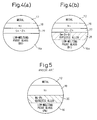
- Fig. 5 is an enlarged view of a sealing portion (A in Fig. 1) in which the light transmitting window 14 is sealed with the cap body using an eutectic reaction between Pb-component contained in the low-melting point glass 16 and Ni in the nickel plated layer 18.
- the reference numeral 12 denotes a metal cap body; 18, a nickel layer plated on the cap body; and 20, an eutectic alloy layer of Ni-Pb.
- An object of the present invention is to provide a semiconductor device cap capable of solving the above-mentioned problems.
- Another object of the present invention is to provide a cap which can be advantageously used in a semiconductor device on which an optical element, such as a laser diode, can be mounted and has a high moisture resistance.
- Still another object of the present invention is to provide a semiconductor device including an optical cap which can be produced using a low-melting point glass, including no lead, as a sealing material during the production processes thereof.
- an optical cap structure for semiconductor device comprising: a cap body having an opening; an optical window made of glass plate sealed with the cap body to cover the opening so that an optical beam transmits through the optical window; and a sealing member for sealing the optical window with the metal cap, the sealing member including a bismuth low-melting point glass containing no lead, an intermediate metal layer attached to the metal cap body, the intermediate metal layer being a metal capable of causing an eutectic reaction with respect to Bi contained in the low-melting point glass, and an eutectic alloy layer thus formed between the low-melting point glass and the intermediate metal layer.
- the intermediate metal is a plated gold, so that the optical window is sealed with the cap body by means of the eutectic alloy between Bi contained in the low-melting point glass and Au of the intermediate metal.
- the intermediate metal is a plated palladium, so that the optical window is sealed with the cap body by means of the eutectic alloy between Bi contained in the low-melting point glass and Pd of the intermediate metal.
- the intermediate metal is a Sn-Ni alloy plated layer, so that the optical window is sealed with the cap body by means of the eutectic alloy between Bi contained in the low-melting point glass and Sn-Ni alloy of the intermediate metal.
- the intermediate metal is a Zn-Ni alloy plated layer, so that the optical window is sealed with the cap body by means of the eutectic alloy between Bi contained in the low-melting point glass and Zn-Ni alloy of the intermediate metal.
- the intermediate metal is a Sn-Zn alloy plated layer, so that the optical window is sealed with the cap body by means of the eutectic alloy between Bi contained in the low-melting point glass and Sn-Zn alloy of the intermediate metal.
- the low-melting point glass contains not less than 30 weight % of Bi.
- a first surface of the intermediate metal opposite to a second surface attached to the metal cap body is a rough surface, a crystal particle size of the first surface being 0.5 ⁇ m to 1.0 ⁇ m.
- the intermediate metal attached to the metal cap body comprises multiple plated metal layers, at least one of the metal layers having a rough surface, a crystal particle size of which being 0.5 ⁇ m to 1.0 ⁇ m.
- an optical device comprising: a stem; an optical element mounted on the stem; a cap body secured on the stem to accommodate therein the optical element, the cap body having an opening; an optical window made of glass plate sealed with the cap body to cover the opening so that an optical beam transmits through the optical window; and a sealing member for sealing the optical window with the metal cap, the sealing member including a bismuth low-melting point glass containing no lead, an intermediate metal layer attached on the metal cap body, the intermediate metal layer being a metal capable of eutectic reaction with respect to Bi contained in the low-melting point glass, and an eutectic alloy layer thus formed between the low-melting point glass and the intermediate metal layer.
- a method of sealing an optical window, made of a glass plate, with a metal cap body, having an opening, for making an optical cap structure for semiconductor device comprising the following steps of: attaching an intermediate metal layer to the metal cap body, the intermediate metal layer being a metal capable of causing an eutectic reaction with respect to Bi contained in a bismuth low-melting point glass containing no lead; setting the optical window and the cap body on a jig in such a manner that a sealing member including the low-melting point glass is placed between the intermediate metal layer and the optical window; and inserting the jig in a furnace to heat the same up to a temperature at which an eutectic reaction is caused between Bi contained in the low-melting point glass and a metal of the intermediate metal layer to seal the window with the cap body.
- a cap for a semiconductor optical device comprises, as shown in Figs. 1(a) and 1(b), a cap body 12, a optical transmission window 14 made of a glass plate sealed with the cap body 12 using a low-melting point glass as a sealing material.
- the cap body 12 is cap-like configuration formed by a press-forming process of a metal plate and has an upper portion provided with an optical transmission opening 12a.
- the optical transmission window 14 is sealed with a peripheral region of the optical transmission opening 12a by a low-melting point glass 16.
- the material of the cap body 12 is not limited, but may advantageously be iron, iron-nickel alloy, or iron-cobalt-nickel alloy.
- the sealing material for sealing the optical transmission window 14 with the cap body 12 is a bismuth low-melting point glass containing no lead, in place of a low-melting point glass containing lead which has been conventionally used in the prior art; and that an intermediate metal layer, which is capable of effecting an eutectic reaction with Bi contained in the bismuth low-melting point glass, is attached to the surface of the cap body so that, when the optical transmission window 14 is sealed with the cap body 12, at the sealing temperature, an eutectic alloy layer is formed at a boundary between the cap body 12 and the low-melting point glass 16 by an eutectic reaction between a metal of the intermediate metal layer and Bi contained in the low-melting point glass.
- the optical transmission window 14 is sealed with the metal cap 12 by the bismuth low-melting point glass 16 and the eutectic alloy layer 24.
- the metal capable of effecting an eutectic reaction with Bi contained in the bismuth low-melting point glass when the optical transmission window 14 is sealed with the cap body 12 may be Au, Ag, Sn, Zn, Pd or any other metal. Therefore, a metal, such as Au, Ag, Sn, Zn, Pd or another, is beforehand attached, such as by plating, to the surface of the metal cap 12. Thus, when the optical transmission window 14 is sealed with the cap body 12, the eutectic alloy is formed between Bi and a metal, such as listed above, to air-tightly seal the optical transmission window 14 with the cap body 12.
- the thickness of the intermediate metal layer capable of effecting an eutectic reaction with Bi may be a thickness sufficient to form an eutectic alloy layer on the surface of the cap body 12.
- the component of bismuth low-melting point glass which can be used in this invention may not be limited, those containing at least SiO 2 , Al 2 O 3 , MgO, ZnO, or Bi 2 O 3 can advantageously be used in the embodiment.
- Bi 2 O 3 is a main component of bismuth low-melting point glass and, in the embodiment, bismuth low-melting point glass contains 50 weight percent of Bi 2 O 3 .
- Bi 2 O 3 is a material which effects an eutectic reaction with a metal attached to the cap body 12 to air-tightly seal the optical transmission window 14 with the cap body 12, a substantial amount (at least 30 weight %) of Bi 2 O 3 must be contained in the low-melting point glass.
- the bismuth low-melting point glass may be a ring-shaped powder tablet corresponding to a dimension of the optical transmission opening 12a of the cap body 12 and may be set on a jig with the cap body 12 and the optical transmission window 14, or may be a paste which is beforehand coated on the optical transmission window 14.
- the cap body 12 is first plated with nickel as an underlayer and then plated with gold. Both nickel-plating and gold-plating are conducted as an electro-plating in a barrel on the entire surface of the cap body 12.
- the thickness of the plated nickel is approximately 2 ⁇ m and the thickness of the plated gold is approximately 0.1 ⁇ m.
- the thickness of 0.1 ⁇ m of the gold-plated layer is sufficient to form an eutectic alloy layer with Bi contained in the low-melting point glass.
- the cap body 12 a tablet of low-melting point glass and the optical transmission window 14 are set onto a jig which is used for heat-sealing the optical transmission window 14 with the cap body 12.
- the cap body 12, a tablet of low-melting point glass and the optical transmission window 14, while being set on the jig, are inserted into a furnace, where they are heated up to a temperature of approximately 500°C in nitrogen gas environment to melt the low-melting point glass so that the optical transmission window 14 is sealed with the cap body 12.
- a eutectic reaction is caused between the plated Au attached to the cap body 12 and Bi contained in the low-melting point glass to form an eutectic alloy layer of Au-Bi and thus the optical transmission window 14 is firmly sealed with the cap body 12.
- a eutectic reaction between Au and Bi can be effected at a temperature of approximately 240°C and thus such an eutectic alloy layer of Au-Bi is simultaneously formed when the low-melting point glass is heated and melted.
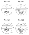
- Figs. 2(a) and 2(b) are enlarged views of the sealing portion between the optical transmission window 14 and the cap body 12 indicated by A in Fig. 1, illustrating before and after, respectively, in which the optical transmission window 14 is sealed with the cap body 12 by means of a bismuth low-melting point glass 16a.
- the cap body 12 is first plated with nickel as an underlayer 18 and then plated with gold 22 on the plated nickel layer 18.
- both Au of the plated gold layer 22 and Bi contained in the low-melting point glass 16a are diffused to cause an eutectic reaction and, therefore, an eutectic alloy layer 24 of Au-Bi is formed at the boundary between the cap body 12 and the optical transmission window 14 and thus the optical transmission window 14 is air-tightly sealed with the cap body 12 by the thus formed eutectic alloy layer 24 of Au-Bi.
- Figs. 3(a) and 3(b) show another embodiment of the sealing portion, illustrating before and after, respectively, the optical transmission window 14 is sealed with the cap body 12 by means of a bismuth low-melting point glass 16a in the same manner as the previous embodiment.
- the cap body 12 is first plated with nickel as an underlayer in the same manner as the previous embodiment, but then plated with palladium 25 on the plated nickel layer 18.
- the thickness of the palladium plated layer 25 is 0.1 ⁇ m.
- An eutectic reaction between Pd and Bi can be effected at a temperature of approximately 256°C. Therefore, at a temperature of approximately 500°C in the furnace, an eutectic reaction is caused and, therefore, a eutectic alloy layer 24 of Pd-Bi is formed at the boundary between the cap body 12 and the optical transmission window 14 and thus the optical transmission window 14 is air-tightly sealed with the cap body 12 by the thus formed eutectic alloy layer 24 of Pd-Bi.
- the surface of the metal cap 12 is lustrous, but in this embodiment, in which the palladium plated layer is formed on the cap body 12, the surface of the metal cap 12 is lusterless and rough as compared with the gold plated layer. Therefore, light reflection at the inside surface of the cap can more effectively be prevented.
- the nickel plated layer 18, as an underlayer of the palladium plated layer is formed so as to have a rough surface, it seems that the optical transmission window 14 can more tightly be sealed with the cap body 12 due to a so-called an "anchor effect" between the nickel plated layer 18 and the palladium plated layer 25.
- Table 1 shows experimental results of the adhering strength of the optical transmission window 14 with respect to the cap body 12 in this embodiment, comparing the case in which the nickel plated layer 18 is formed in a usual manner, with the case in which the nickel plated layer 18 is formed to have a rough surface.
- Pd/Ni Ni Plated Underlayer Adhering Strength 1 Usual Surface Plating 3.8 kgf 2 ⁇ Rough Surface Plating 4.9 kgf
- the thickness of the nickel plated underlayer 18 is 2 ⁇ m to 9 ⁇ m, and the crystal particle size is 0.5 ⁇ m to 1.0 ⁇ m.
- the nickel plated underlayer 18 is formed so as to have a rough surface
- a rough surface of the nickel plated underlayer 18 or the intermediate metal layer capable of effecting an eutectic reaction with Bi may be formed by any appropriate process, such as a plating process for forming such a rough surface, a chemical process, such as etching, or physical process, such as sand-blasting.
- Figs. 4(a) and 4(b) show a third embodiment of the sealing portion, illustrating before and after, respectively, the optical transmission window 14 is sealed with the cap body 12 by means of a bismuth low-melting point glass 16a in the same manner as the previous embodiments.
- the cap body 12 is first plated with nickel as an underlayer, in the same manner as the previous embodiments, and is then plated with Sn-Zn alloy layer 27 on the plated nickel layer 18.
- the temperature at which an eutectic reaction is developed between Bi and Sn-Zn alloy is approximately 200°C. Therefore, during the operation of sealing the optical transmission window 14 with the cap body 12, an eutectic alloy layer 28 of Sn-Zn-Bi is formed at the boundary between the cap body 12 and the bismuth low-melting point glass 16a, so that the optical transmission window 14 is air-tightly sealed with the cap body 12 by thus formed eutectic alloy layer 28 of Sn-Zn-Bi.
- the temperature at which an eutectic reaction is caused between Bi and Sn is approximately 140°C
- between Bi and Sn is approximately 254°C
- between Bi and Ag is approximately 260°C. Therefore, in the same manner as the previous embodiments, an Sn-Ni alloy, or Zn-Ni alloy, or silver can be plated on the surface of the cap body 12.
- an eutectic alloy layer of Sn-Bi, an eutectic alloy layer of Zn-Bi, and an eutectic alloy layer of Ag-Bi can be formed at the boundary between the cap body 12 and the bismuth low-melting point glass 16a, so that the optical transmission window 14 is air-tightly sealed with the cap body 12 by thus formed eutectic alloy layer, in the same manner as the previous embodiments.
- the surface of the cap body 12 becomes rough, so that, in the same manner as the case in which palladium is plated on the surface of the cap body 12, light reflection at the inside surface of the cap can more effectively be prevented and a generation of noise in the semiconductor device is also more effectively restricted as compared with the case in which a gold is plated.
- a cap for semiconductor device is constructed by means of a bismuth low-melting point glass 16a, containing no lead, as a sealing material for sealing the optical transmitting window 14 to the cap body 12. Therefore, a "no-lead" process for manufacturing the cap of semiconductor device can be attained.
- a eutectic alloy layer is formed between Bi contained in the bismuth low-melting point glass 16a and an intermediate metal attached to the surface of the cap body, such as plating, so that the optical transmitting window is sealed with the cap body 12 by means of thus formed eutectic alloy layer. Therefore, the optical transmitting window can be more reliably sealed with the cap body 12 with high air-tight and moisture endurable performance and thus the cap can be advantageously used for a semiconductor device accommodating therein an optical element, such as a laser diode.
Landscapes
- Physics & Mathematics (AREA)
- Condensed Matter Physics & Semiconductors (AREA)
- General Physics & Mathematics (AREA)
- Electromagnetism (AREA)
- Optics & Photonics (AREA)
- Semiconductor Lasers (AREA)
- Led Device Packages (AREA)
- Light Receiving Elements (AREA)
Applications Claiming Priority (6)
| Application Number | Priority Date | Filing Date | Title |
|---|---|---|---|
| JP2003101222 | 2003-04-04 | ||
| JP2003101222 | 2003-04-04 | ||
| JP2003312128 | 2003-09-04 | ||
| JP2003312128 | 2003-09-04 | ||
| JP2003379849 | 2003-11-10 | ||
| JP2003379849A JP3655916B2 (ja) | 2003-04-04 | 2003-11-10 | 半導体装置用キャップ |
Publications (3)
| Publication Number | Publication Date |
|---|---|
| EP1465263A2 true EP1465263A2 (de) | 2004-10-06 |
| EP1465263A3 EP1465263A3 (de) | 2010-11-17 |
| EP1465263B1 EP1465263B1 (de) | 2012-01-25 |
Family
ID=32854127
Family Applications (1)
| Application Number | Title | Priority Date | Filing Date |
|---|---|---|---|
| EP04007711A Expired - Lifetime EP1465263B1 (de) | 2003-04-04 | 2004-03-30 | Deckel für optische Halbleiteranordnung |
Country Status (3)
| Country | Link |
|---|---|
| US (1) | US6984849B2 (de) |
| EP (1) | EP1465263B1 (de) |
| JP (1) | JP3655916B2 (de) |
Cited By (1)
| Publication number | Priority date | Publication date | Assignee | Title |
|---|---|---|---|---|
| CN112208735A (zh) * | 2020-08-20 | 2021-01-12 | 山东航天电子技术研究所 | 一种水下激光探测系统密封舱体 |
Families Citing this family (18)
| Publication number | Priority date | Publication date | Assignee | Title |
|---|---|---|---|---|
| JP2005303242A (ja) * | 2004-03-19 | 2005-10-27 | Hitachi Cable Ltd | 冷却機能付き電気−光変換モジュール |
| JP4374300B2 (ja) * | 2004-09-02 | 2009-12-02 | 新光電気工業株式会社 | 半導体装置用キャップ |
| DE102005063312B4 (de) * | 2005-01-27 | 2007-08-23 | Carl Zeiss Vision Gmbh | Transportvorrichtung zum Handhaben von Linsen und Haltevorrichtung für diese |
| JP2006327845A (ja) * | 2005-05-24 | 2006-12-07 | Asahi Techno Glass Corp | プレスフリット |
| JP2007094049A (ja) * | 2005-09-29 | 2007-04-12 | Shinko Electric Ind Co Ltd | 光学部品用キャップ及びその製造方法 |
| JP2007165551A (ja) * | 2005-12-13 | 2007-06-28 | Nippon Electric Glass Co Ltd | 光学用キャップ部品 |
| KR100724392B1 (ko) * | 2006-01-03 | 2007-06-04 | 엘지전자 주식회사 | 왕복동식 압축기의 운전제어장치 및 방법 |
| JP2008263099A (ja) * | 2007-04-13 | 2008-10-30 | Shinko Electric Ind Co Ltd | 光半導体素子用パッケージ及び光ピックアップ装置 |
| JP5079474B2 (ja) * | 2007-11-29 | 2012-11-21 | シャープ株式会社 | キャップ部材およびそれを用いた半導体装置 |
| WO2010021267A1 (ja) * | 2008-08-21 | 2010-02-25 | 株式会社村田製作所 | 電子部品装置およびその製造方法 |
| WO2015010061A2 (en) * | 2013-07-19 | 2015-01-22 | Materion Corporation | A metal cap assembly for optical communications |
| JP7148793B2 (ja) * | 2018-09-27 | 2022-10-06 | 日亜化学工業株式会社 | 光半導体装置用金属材料、及びその製造方法、及びそれを用いた光半導体装置 |
| JP7148792B2 (ja) | 2018-09-27 | 2022-10-06 | 日亜化学工業株式会社 | 光半導体装置用金属材料、及びその製造方法、及びそれを用いた光半導体装置 |
| KR102656315B1 (ko) * | 2018-10-05 | 2024-04-09 | 에이지씨 가부시키가이샤 | 창재, 광학 패키지 |
| WO2020159613A1 (en) * | 2019-01-31 | 2020-08-06 | The Regents Of The University Of California | Metal to glass seal |
| US11476637B2 (en) * | 2019-12-16 | 2022-10-18 | Nichia Corporation | Light-emitting device |
| CN112259665A (zh) * | 2020-11-14 | 2021-01-22 | 中山市顺为鑫科技有限公司 | 一种高气密性的光窗盖板 |
| JP7579201B2 (ja) | 2021-04-23 | 2024-11-07 | シャープ福山レーザー株式会社 | 発光装置 |
Family Cites Families (8)
| Publication number | Priority date | Publication date | Assignee | Title |
|---|---|---|---|---|
| JPS5946434B2 (ja) * | 1978-01-10 | 1984-11-12 | キヤノン株式会社 | 半導体レ−ザ装置 |
| US5013360A (en) * | 1989-09-15 | 1991-05-07 | Vlsi Packaging Materials, Inc. | Sealing glass compositions |
| JPH04270140A (ja) * | 1990-06-21 | 1992-09-25 | Johnson Matthey Inc | シーリングガラス組成物および導電性成分を含む同組成物 |
| JPH0799368A (ja) * | 1993-09-29 | 1995-04-11 | Mitsubishi Electric Corp | 光半導体装置 |
| FR2727962A1 (fr) * | 1994-12-13 | 1996-06-14 | Univ Lille Sciences Tech | Composition de verres a base d'oxydes p205-v205 et leurs applications pour le revetement ou le scellement de ceramiques |
| JP2002084027A (ja) * | 2000-09-07 | 2002-03-22 | Sony Corp | 半導体発光装置 |
| JP3726720B2 (ja) * | 2001-07-05 | 2005-12-14 | ソニー株式会社 | 投受光デバイス構造 |
| JP5071876B2 (ja) * | 2001-07-23 | 2012-11-14 | 日本電気硝子株式会社 | 光透過用金属キャップ |
-
2003
- 2003-11-10 JP JP2003379849A patent/JP3655916B2/ja not_active Expired - Lifetime
-
2004
- 2004-03-30 EP EP04007711A patent/EP1465263B1/de not_active Expired - Lifetime
- 2004-04-01 US US10/814,276 patent/US6984849B2/en not_active Expired - Lifetime
Cited By (1)
| Publication number | Priority date | Publication date | Assignee | Title |
|---|---|---|---|---|
| CN112208735A (zh) * | 2020-08-20 | 2021-01-12 | 山东航天电子技术研究所 | 一种水下激光探测系统密封舱体 |
Also Published As
| Publication number | Publication date |
|---|---|
| JP2005101481A (ja) | 2005-04-14 |
| EP1465263A3 (de) | 2010-11-17 |
| EP1465263B1 (de) | 2012-01-25 |
| US20040195580A1 (en) | 2004-10-07 |
| JP3655916B2 (ja) | 2005-06-02 |
| US6984849B2 (en) | 2006-01-10 |
Similar Documents
| Publication | Publication Date | Title |
|---|---|---|
| EP1465263B1 (de) | Deckel für optische Halbleiteranordnung | |
| US7065867B2 (en) | Low temperature hermetic sealing method having passivation layer | |
| US20060131600A1 (en) | Light transmitting window member, semiconductor package provided with light transmitting window member and method for manufacturing light transmitting window member | |
| JPH0249021B2 (de) | ||
| US4940855A (en) | Hermetically tight glass-metal housing for semiconductor components and method for producing same | |
| US4590672A (en) | Package for electronic device and method for producing same | |
| JP2002033519A (ja) | 光通信用パッケージ及びその窓部材並びにその製造方法 | |
| EP0630868B1 (de) | Flussmittelloses lötverfahren | |
| JP4374300B2 (ja) | 半導体装置用キャップ | |
| JP2970635B2 (ja) | 半導体レーザーモジュール及び金属フェルール | |
| US12237450B2 (en) | Metallic structure for optical semiconductor device, method for producing the same, and optical semiconductor device using the same | |
| JP4456980B2 (ja) | 半導体装置用キャップ | |
| JP2560128B2 (ja) | 半導体レーザ装置 | |
| JP2560129B2 (ja) | 半導体レーザ装置 | |
| JP7116308B2 (ja) | 光半導体装置用金属材料、及びその製造方法、及びそれを用いた光半導体装置 | |
| JP2008263099A (ja) | 光半導体素子用パッケージ及び光ピックアップ装置 | |
| JPS59213189A (ja) | 半導体装置 | |
| JPH06252281A (ja) | 半導体装置用キャップ及びその製造方法 | |
| JPH05102531A (ja) | チツプ部品型発光ダイオード | |
| JP2008263047A (ja) | 光半導体素子用キャップ、光半導体素子用パッケージ及び光ピックアップ装置 | |
| JP2560137B2 (ja) | 半導体レーザ装置 | |
| JP3478559B2 (ja) | 光モジュール用パッケージ及びその製造方法 | |
| JPH11251688A (ja) | 電子部品用キャップおよびそれを用いた半導体レーザ | |
| JPH0448671A (ja) | 半導体レーザ装置における透明樹脂の充填方法 | |
| JPH077098A (ja) | 半導体装置用キャップ及びその製造方法 |
Legal Events
| Date | Code | Title | Description |
|---|---|---|---|
| PUAI | Public reference made under article 153(3) epc to a published international application that has entered the european phase |
Free format text: ORIGINAL CODE: 0009012 |
|
| AK | Designated contracting states |
Kind code of ref document: A2 Designated state(s): AT BE BG CH CY CZ DE DK EE ES FI FR GB GR HU IE IT LI LU MC NL PL PT RO SE SI SK TR |
|
| AX | Request for extension of the european patent |
Extension state: AL LT LV MK |
|
| PUAL | Search report despatched |
Free format text: ORIGINAL CODE: 0009013 |
|
| AK | Designated contracting states |
Kind code of ref document: A3 Designated state(s): AT BE BG CH CY CZ DE DK EE ES FI FR GB GR HU IE IT LI LU MC NL PL PT RO SE SI SK TR |
|
| AX | Request for extension of the european patent |
Extension state: AL LT LV MK |
|
| 17P | Request for examination filed |
Effective date: 20101126 |
|
| RIC1 | Information provided on ipc code assigned before grant |
Ipc: H01L 31/0203 20060101ALI20110429BHEP Ipc: H01L 33/00 20100101AFI20110429BHEP |
|
| AKX | Designation fees paid |
Designated state(s): DE |
|
| GRAP | Despatch of communication of intention to grant a patent |
Free format text: ORIGINAL CODE: EPIDOSNIGR1 |
|
| GRAS | Grant fee paid |
Free format text: ORIGINAL CODE: EPIDOSNIGR3 |
|
| GRAA | (expected) grant |
Free format text: ORIGINAL CODE: 0009210 |
|
| AK | Designated contracting states |
Kind code of ref document: B1 Designated state(s): DE |
|
| REG | Reference to a national code |
Ref country code: DE Ref legal event code: R096 Ref document number: 602004036248 Country of ref document: DE Effective date: 20120322 |
|
| PLBE | No opposition filed within time limit |
Free format text: ORIGINAL CODE: 0009261 |
|
| STAA | Information on the status of an ep patent application or granted ep patent |
Free format text: STATUS: NO OPPOSITION FILED WITHIN TIME LIMIT |
|
| 26N | No opposition filed |
Effective date: 20121026 |
|
| REG | Reference to a national code |
Ref country code: DE Ref legal event code: R097 Ref document number: 602004036248 Country of ref document: DE Effective date: 20121026 |
|
| PGFP | Annual fee paid to national office [announced via postgrant information from national office to epo] |
Ref country code: DE Payment date: 20230131 Year of fee payment: 20 |
|
| REG | Reference to a national code |
Ref country code: DE Ref legal event code: R071 Ref document number: 602004036248 Country of ref document: DE |