EP1467351B1 - Optisches Aufzeichnungsmedium, Verfahren zu dessen Herstellung und Verfahren und Vorrichtung zum Aufzeichnen auf oder Lesen von diesem Medium - Google Patents
Optisches Aufzeichnungsmedium, Verfahren zu dessen Herstellung und Verfahren und Vorrichtung zum Aufzeichnen auf oder Lesen von diesem Medium Download PDFInfo
- Publication number
- EP1467351B1 EP1467351B1 EP04014398A EP04014398A EP1467351B1 EP 1467351 B1 EP1467351 B1 EP 1467351B1 EP 04014398 A EP04014398 A EP 04014398A EP 04014398 A EP04014398 A EP 04014398A EP 1467351 B1 EP1467351 B1 EP 1467351B1
- Authority
- EP
- European Patent Office
- Prior art keywords
- recording
- optical information
- recording medium
- information recording
- layer
- Prior art date
- Legal status (The legal status is an assumption and is not a legal conclusion. Google has not performed a legal analysis and makes no representation as to the accuracy of the status listed.)
- Expired - Lifetime
Links
- 230000003287 optical effect Effects 0.000 title claims description 126
- 238000000034 method Methods 0.000 title claims description 22
- 230000008859 change Effects 0.000 claims description 40
- 239000000203 mixture Substances 0.000 claims description 24
- 239000000463 material Substances 0.000 claims description 22
- 239000000758 substrate Substances 0.000 claims description 17
- 229910052733 gallium Inorganic materials 0.000 claims description 13
- 229910052732 germanium Inorganic materials 0.000 claims description 13
- 229910052714 tellurium Inorganic materials 0.000 claims description 12
- 229910052787 antimony Inorganic materials 0.000 claims description 11
- 229910052718 tin Inorganic materials 0.000 claims description 9
- 229910052737 gold Inorganic materials 0.000 claims description 8
- 229910052709 silver Inorganic materials 0.000 claims description 8
- 229910052802 copper Inorganic materials 0.000 claims description 7
- 229910052782 aluminium Inorganic materials 0.000 claims description 6
- 229910052763 palladium Inorganic materials 0.000 claims description 6
- 229910052797 bismuth Inorganic materials 0.000 claims description 5
- 229910052799 carbon Inorganic materials 0.000 claims description 5
- 229910052697 platinum Inorganic materials 0.000 claims description 5
- 229910052719 titanium Inorganic materials 0.000 claims description 5
- 229910052804 chromium Inorganic materials 0.000 claims description 4
- 229910052738 indium Inorganic materials 0.000 claims description 4
- 229910052757 nitrogen Inorganic materials 0.000 claims description 4
- 229910052725 zinc Inorganic materials 0.000 claims description 4
- 230000007423 decrease Effects 0.000 claims description 3
- 229910052748 manganese Inorganic materials 0.000 claims description 3
- 229910052750 molybdenum Inorganic materials 0.000 claims description 3
- 229910052758 niobium Inorganic materials 0.000 claims description 3
- 229910052703 rhodium Inorganic materials 0.000 claims description 3
- 229910052717 sulfur Inorganic materials 0.000 claims description 3
- 229910052720 vanadium Inorganic materials 0.000 claims description 3
- 229910052726 zirconium Inorganic materials 0.000 claims description 3
- 239000010410 layer Substances 0.000 description 126
- 230000035945 sensitivity Effects 0.000 description 15
- 230000003252 repetitive effect Effects 0.000 description 13
- 239000000956 alloy Substances 0.000 description 10
- 238000004321 preservation Methods 0.000 description 10
- 229910045601 alloy Inorganic materials 0.000 description 9
- 238000002310 reflectometry Methods 0.000 description 9
- 238000010586 diagram Methods 0.000 description 7
- 229920005989 resin Polymers 0.000 description 7
- 239000011347 resin Substances 0.000 description 7
- VYPSYNLAJGMNEJ-UHFFFAOYSA-N Silicium dioxide Chemical compound O=[Si]=O VYPSYNLAJGMNEJ-UHFFFAOYSA-N 0.000 description 6
- 238000002425 crystallisation Methods 0.000 description 6
- 230000008025 crystallization Effects 0.000 description 6
- 230000006872 improvement Effects 0.000 description 6
- 238000004544 sputter deposition Methods 0.000 description 6
- 229910000763 AgInSbTe Inorganic materials 0.000 description 5
- 238000001816 cooling Methods 0.000 description 5
- 238000005516 engineering process Methods 0.000 description 5
- 239000010408 film Substances 0.000 description 5
- 238000007740 vapor deposition Methods 0.000 description 5
- 230000015556 catabolic process Effects 0.000 description 4
- 150000001875 compounds Chemical class 0.000 description 4
- 230000003247 decreasing effect Effects 0.000 description 4
- 238000006731 degradation reaction Methods 0.000 description 4
- 238000004519 manufacturing process Methods 0.000 description 4
- 238000002844 melting Methods 0.000 description 4
- 230000008018 melting Effects 0.000 description 4
- -1 polypropylene Polymers 0.000 description 4
- 239000004065 semiconductor Substances 0.000 description 4
- 229910005900 GeTe Inorganic materials 0.000 description 3
- 238000005229 chemical vapour deposition Methods 0.000 description 3
- 229910052681 coesite Inorganic materials 0.000 description 3
- 239000000470 constituent Substances 0.000 description 3
- 229910052906 cristobalite Inorganic materials 0.000 description 3
- 239000013078 crystal Substances 0.000 description 3
- 238000000151 deposition Methods 0.000 description 3
- 238000007733 ion plating Methods 0.000 description 3
- 238000005268 plasma chemical vapour deposition Methods 0.000 description 3
- 230000009467 reduction Effects 0.000 description 3
- 229910052710 silicon Inorganic materials 0.000 description 3
- 239000000377 silicon dioxide Substances 0.000 description 3
- 238000004528 spin coating Methods 0.000 description 3
- 229910052682 stishovite Inorganic materials 0.000 description 3
- 239000000126 substance Substances 0.000 description 3
- 239000010409 thin film Substances 0.000 description 3
- 229910052905 tridymite Inorganic materials 0.000 description 3
- 238000001771 vacuum deposition Methods 0.000 description 3
- 229920000178 Acrylic resin Polymers 0.000 description 2
- 239000004925 Acrylic resin Substances 0.000 description 2
- 229910000838 Al alloy Inorganic materials 0.000 description 2
- CPLXHLVBOLITMK-UHFFFAOYSA-N Magnesium oxide Chemical compound [Mg]=O CPLXHLVBOLITMK-UHFFFAOYSA-N 0.000 description 2
- 229910018219 SeTe Inorganic materials 0.000 description 2
- GWEVSGVZZGPLCZ-UHFFFAOYSA-N Titan oxide Chemical compound O=[Ti]=O GWEVSGVZZGPLCZ-UHFFFAOYSA-N 0.000 description 2
- XLOMVQKBTHCTTD-UHFFFAOYSA-N Zinc monoxide Chemical compound [Zn]=O XLOMVQKBTHCTTD-UHFFFAOYSA-N 0.000 description 2
- MCMNRKCIXSYSNV-UHFFFAOYSA-N Zirconium dioxide Chemical compound O=[Zr]=O MCMNRKCIXSYSNV-UHFFFAOYSA-N 0.000 description 2
- 239000000654 additive Substances 0.000 description 2
- 230000000996 additive effect Effects 0.000 description 2
- 238000007796 conventional method Methods 0.000 description 2
- 230000000694 effects Effects 0.000 description 2
- 238000011156 evaluation Methods 0.000 description 2
- 230000001678 irradiating effect Effects 0.000 description 2
- 150000004767 nitrides Chemical class 0.000 description 2
- 239000004417 polycarbonate Substances 0.000 description 2
- 229920000515 polycarbonate Polymers 0.000 description 2
- 229920005668 polycarbonate resin Polymers 0.000 description 2
- 239000004431 polycarbonate resin Substances 0.000 description 2
- 230000002265 prevention Effects 0.000 description 2
- 238000011160 research Methods 0.000 description 2
- FESBVLZDDCQLFY-UHFFFAOYSA-N sete Chemical compound [Te]=[Se] FESBVLZDDCQLFY-UHFFFAOYSA-N 0.000 description 2
- LIVNPJMFVYWSIS-UHFFFAOYSA-N silicon monoxide Chemical compound [Si-]#[O+] LIVNPJMFVYWSIS-UHFFFAOYSA-N 0.000 description 2
- 239000002356 single layer Substances 0.000 description 2
- 229910052715 tantalum Inorganic materials 0.000 description 2
- XOLBLPGZBRYERU-UHFFFAOYSA-N tin dioxide Chemical compound O=[Sn]=O XOLBLPGZBRYERU-UHFFFAOYSA-N 0.000 description 2
- 229910017083 AlN Inorganic materials 0.000 description 1
- OKTJSMMVPCPJKN-UHFFFAOYSA-N Carbon Chemical compound [C] OKTJSMMVPCPJKN-UHFFFAOYSA-N 0.000 description 1
- 229910005918 GeTeSe Inorganic materials 0.000 description 1
- 239000004743 Polypropylene Substances 0.000 description 1
- 229910017629 Sb2Te3 Inorganic materials 0.000 description 1
- 229910052581 Si3N4 Inorganic materials 0.000 description 1
- UCKMPCXJQFINFW-UHFFFAOYSA-N Sulphide Chemical compound [S-2] UCKMPCXJQFINFW-UHFFFAOYSA-N 0.000 description 1
- ATJFFYVFTNAWJD-UHFFFAOYSA-N Tin Chemical compound [Sn] ATJFFYVFTNAWJD-UHFFFAOYSA-N 0.000 description 1
- 229920000122 acrylonitrile butadiene styrene Polymers 0.000 description 1
- 229920001893 acrylonitrile styrene Polymers 0.000 description 1
- PNEYBMLMFCGWSK-UHFFFAOYSA-N aluminium oxide Inorganic materials [O-2].[O-2].[O-2].[Al+3].[Al+3] PNEYBMLMFCGWSK-UHFFFAOYSA-N 0.000 description 1
- 229910052785 arsenic Inorganic materials 0.000 description 1
- 230000008901 benefit Effects 0.000 description 1
- 239000000919 ceramic Substances 0.000 description 1
- 229910052798 chalcogen Inorganic materials 0.000 description 1
- 150000001787 chalcogens Chemical class 0.000 description 1
- 229920006026 co-polymeric resin Polymers 0.000 description 1
- 239000004020 conductor Substances 0.000 description 1
- 229910052593 corundum Inorganic materials 0.000 description 1
- 238000011161 development Methods 0.000 description 1
- 230000018109 developmental process Effects 0.000 description 1
- 229910003460 diamond Inorganic materials 0.000 description 1
- 239000010432 diamond Substances 0.000 description 1
- 239000003822 epoxy resin Substances 0.000 description 1
- 239000004744 fabric Substances 0.000 description 1
- 239000011521 glass Substances 0.000 description 1
- 239000012535 impurity Substances 0.000 description 1
- PJXISJQVUVHSOJ-UHFFFAOYSA-N indium(III) oxide Inorganic materials [O-2].[O-2].[O-2].[In+3].[In+3] PJXISJQVUVHSOJ-UHFFFAOYSA-N 0.000 description 1
- 238000011835 investigation Methods 0.000 description 1
- 229910052745 lead Inorganic materials 0.000 description 1
- 238000005259 measurement Methods 0.000 description 1
- 230000007246 mechanism Effects 0.000 description 1
- 229910052751 metal Inorganic materials 0.000 description 1
- 239000002184 metal Substances 0.000 description 1
- 150000001247 metal acetylides Chemical class 0.000 description 1
- 229910044991 metal oxide Inorganic materials 0.000 description 1
- 150000004706 metal oxides Chemical class 0.000 description 1
- 150000002739 metals Chemical class 0.000 description 1
- 238000012544 monitoring process Methods 0.000 description 1
- 238000007254 oxidation reaction Methods 0.000 description 1
- 229910052760 oxygen Inorganic materials 0.000 description 1
- 229920000647 polyepoxide Polymers 0.000 description 1
- 229920013716 polyethylene resin Polymers 0.000 description 1
- 229920001155 polypropylene Polymers 0.000 description 1
- 229920005990 polystyrene resin Polymers 0.000 description 1
- SCUZVMOVTVSBLE-UHFFFAOYSA-N prop-2-enenitrile;styrene Chemical compound C=CC#N.C=CC1=CC=CC=C1 SCUZVMOVTVSBLE-UHFFFAOYSA-N 0.000 description 1
- 238000001953 recrystallisation Methods 0.000 description 1
- 229910052711 selenium Inorganic materials 0.000 description 1
- 238000000926 separation method Methods 0.000 description 1
- 229920002050 silicone resin Polymers 0.000 description 1
- 238000012360 testing method Methods 0.000 description 1
- 230000003685 thermal hair damage Effects 0.000 description 1
- 229920002803 thermoplastic polyurethane Polymers 0.000 description 1
- 230000007704 transition Effects 0.000 description 1
- 229910052721 tungsten Inorganic materials 0.000 description 1
- 229910001845 yogo sapphire Inorganic materials 0.000 description 1
Images


Classifications
-
- G—PHYSICS
- G11—INFORMATION STORAGE
- G11B—INFORMATION STORAGE BASED ON RELATIVE MOVEMENT BETWEEN RECORD CARRIER AND TRANSDUCER
- G11B19/00—Driving, starting, stopping record carriers not specifically of filamentary or web form, or of supports therefor; Control thereof; Control of operating function ; Driving both disc and head
- G11B19/20—Driving; Starting; Stopping; Control thereof
- G11B19/26—Speed-changing arrangements; Reversing arrangements; Drive-transfer means therefor
-
- G—PHYSICS
- G11—INFORMATION STORAGE
- G11B—INFORMATION STORAGE BASED ON RELATIVE MOVEMENT BETWEEN RECORD CARRIER AND TRANSDUCER
- G11B19/00—Driving, starting, stopping record carriers not specifically of filamentary or web form, or of supports therefor; Control thereof; Control of operating function ; Driving both disc and head
- G11B19/02—Control of operating function, e.g. switching from recording to reproducing
- G11B19/12—Control of operating function, e.g. switching from recording to reproducing by sensing distinguishing features of or on records, e.g. diameter end mark
-
- G—PHYSICS
- G11—INFORMATION STORAGE
- G11B—INFORMATION STORAGE BASED ON RELATIVE MOVEMENT BETWEEN RECORD CARRIER AND TRANSDUCER
- G11B20/00—Signal processing not specific to the method of recording or reproducing; Circuits therefor
- G11B20/02—Analogue recording or reproducing
- G11B20/08—Pulse-modulation recording or reproducing
-
- G—PHYSICS
- G11—INFORMATION STORAGE
- G11B—INFORMATION STORAGE BASED ON RELATIVE MOVEMENT BETWEEN RECORD CARRIER AND TRANSDUCER
- G11B20/00—Signal processing not specific to the method of recording or reproducing; Circuits therefor
- G11B20/10—Digital recording or reproducing
-
- G—PHYSICS
- G11—INFORMATION STORAGE
- G11B—INFORMATION STORAGE BASED ON RELATIVE MOVEMENT BETWEEN RECORD CARRIER AND TRANSDUCER
- G11B7/00—Recording or reproducing by optical means, e.g. recording using a thermal beam of optical radiation by modifying optical properties or the physical structure, reproducing using an optical beam at lower power by sensing optical properties; Record carriers therefor
- G11B7/004—Recording, reproducing or erasing methods; Read, write or erase circuits therefor
- G11B7/0045—Recording
- G11B7/00454—Recording involving phase-change effects
-
- G—PHYSICS
- G11—INFORMATION STORAGE
- G11B—INFORMATION STORAGE BASED ON RELATIVE MOVEMENT BETWEEN RECORD CARRIER AND TRANSDUCER
- G11B7/00—Recording or reproducing by optical means, e.g. recording using a thermal beam of optical radiation by modifying optical properties or the physical structure, reproducing using an optical beam at lower power by sensing optical properties; Record carriers therefor
- G11B7/004—Recording, reproducing or erasing methods; Read, write or erase circuits therefor
- G11B7/005—Reproducing
- G11B7/0052—Reproducing involving reflectivity, absorption or colour changes
-
- G—PHYSICS
- G11—INFORMATION STORAGE
- G11B—INFORMATION STORAGE BASED ON RELATIVE MOVEMENT BETWEEN RECORD CARRIER AND TRANSDUCER
- G11B7/00—Recording or reproducing by optical means, e.g. recording using a thermal beam of optical radiation by modifying optical properties or the physical structure, reproducing using an optical beam at lower power by sensing optical properties; Record carriers therefor
- G11B7/004—Recording, reproducing or erasing methods; Read, write or erase circuits therefor
- G11B7/006—Overwriting
-
- G—PHYSICS
- G11—INFORMATION STORAGE
- G11B—INFORMATION STORAGE BASED ON RELATIVE MOVEMENT BETWEEN RECORD CARRIER AND TRANSDUCER
- G11B7/00—Recording or reproducing by optical means, e.g. recording using a thermal beam of optical radiation by modifying optical properties or the physical structure, reproducing using an optical beam at lower power by sensing optical properties; Record carriers therefor
- G11B7/007—Arrangement of the information on the record carrier, e.g. form of tracks, actual track shape, e.g. wobbled, or cross-section, e.g. v-shaped; Sequential information structures, e.g. sectoring or header formats within a track
-
- G—PHYSICS
- G11—INFORMATION STORAGE
- G11B—INFORMATION STORAGE BASED ON RELATIVE MOVEMENT BETWEEN RECORD CARRIER AND TRANSDUCER
- G11B7/00—Recording or reproducing by optical means, e.g. recording using a thermal beam of optical radiation by modifying optical properties or the physical structure, reproducing using an optical beam at lower power by sensing optical properties; Record carriers therefor
- G11B7/12—Heads, e.g. forming of the optical beam spot or modulation of the optical beam
- G11B7/125—Optical beam sources therefor, e.g. laser control circuitry specially adapted for optical storage devices; Modulators, e.g. means for controlling the size or intensity of optical spots or optical traces
- G11B7/126—Circuits, methods or arrangements for laser control or stabilisation
-
- G—PHYSICS
- G11—INFORMATION STORAGE
- G11B—INFORMATION STORAGE BASED ON RELATIVE MOVEMENT BETWEEN RECORD CARRIER AND TRANSDUCER
- G11B7/00—Recording or reproducing by optical means, e.g. recording using a thermal beam of optical radiation by modifying optical properties or the physical structure, reproducing using an optical beam at lower power by sensing optical properties; Record carriers therefor
- G11B7/24—Record carriers characterised by shape, structure or physical properties, or by the selection of the material
- G11B7/241—Record carriers characterised by shape, structure or physical properties, or by the selection of the material characterised by the selection of the material
- G11B7/242—Record carriers characterised by shape, structure or physical properties, or by the selection of the material characterised by the selection of the material of recording layers
- G11B7/243—Record carriers characterised by shape, structure or physical properties, or by the selection of the material characterised by the selection of the material of recording layers comprising inorganic materials only, e.g. ablative layers
-
- G—PHYSICS
- G11—INFORMATION STORAGE
- G11B—INFORMATION STORAGE BASED ON RELATIVE MOVEMENT BETWEEN RECORD CARRIER AND TRANSDUCER
- G11B7/00—Recording or reproducing by optical means, e.g. recording using a thermal beam of optical radiation by modifying optical properties or the physical structure, reproducing using an optical beam at lower power by sensing optical properties; Record carriers therefor
- G11B7/24—Record carriers characterised by shape, structure or physical properties, or by the selection of the material
- G11B7/26—Apparatus or processes specially adapted for the manufacture of record carriers
-
- G—PHYSICS
- G11—INFORMATION STORAGE
- G11B—INFORMATION STORAGE BASED ON RELATIVE MOVEMENT BETWEEN RECORD CARRIER AND TRANSDUCER
- G11B7/00—Recording or reproducing by optical means, e.g. recording using a thermal beam of optical radiation by modifying optical properties or the physical structure, reproducing using an optical beam at lower power by sensing optical properties; Record carriers therefor
- G11B7/24—Record carriers characterised by shape, structure or physical properties, or by the selection of the material
- G11B7/241—Record carriers characterised by shape, structure or physical properties, or by the selection of the material characterised by the selection of the material
- G11B7/242—Record carriers characterised by shape, structure or physical properties, or by the selection of the material characterised by the selection of the material of recording layers
- G11B7/243—Record carriers characterised by shape, structure or physical properties, or by the selection of the material characterised by the selection of the material of recording layers comprising inorganic materials only, e.g. ablative layers
- G11B2007/24302—Metals or metalloids
- G11B2007/24314—Metals or metalloids group 15 elements (e.g. Sb, Bi)
-
- G—PHYSICS
- G11—INFORMATION STORAGE
- G11B—INFORMATION STORAGE BASED ON RELATIVE MOVEMENT BETWEEN RECORD CARRIER AND TRANSDUCER
- G11B7/00—Recording or reproducing by optical means, e.g. recording using a thermal beam of optical radiation by modifying optical properties or the physical structure, reproducing using an optical beam at lower power by sensing optical properties; Record carriers therefor
- G11B7/24—Record carriers characterised by shape, structure or physical properties, or by the selection of the material
- G11B7/241—Record carriers characterised by shape, structure or physical properties, or by the selection of the material characterised by the selection of the material
- G11B7/242—Record carriers characterised by shape, structure or physical properties, or by the selection of the material characterised by the selection of the material of recording layers
- G11B7/243—Record carriers characterised by shape, structure or physical properties, or by the selection of the material characterised by the selection of the material of recording layers comprising inorganic materials only, e.g. ablative layers
- G11B2007/24302—Metals or metalloids
- G11B2007/24316—Metals or metalloids group 16 elements (i.e. chalcogenides, Se, Te)
-
- G—PHYSICS
- G11—INFORMATION STORAGE
- G11B—INFORMATION STORAGE BASED ON RELATIVE MOVEMENT BETWEEN RECORD CARRIER AND TRANSDUCER
- G11B7/00—Recording or reproducing by optical means, e.g. recording using a thermal beam of optical radiation by modifying optical properties or the physical structure, reproducing using an optical beam at lower power by sensing optical properties; Record carriers therefor
- G11B7/004—Recording, reproducing or erasing methods; Read, write or erase circuits therefor
- G11B7/006—Overwriting
- G11B7/0062—Overwriting strategies, e.g. recording pulse sequences with erasing level used for phase-change media
-
- G—PHYSICS
- G11—INFORMATION STORAGE
- G11B—INFORMATION STORAGE BASED ON RELATIVE MOVEMENT BETWEEN RECORD CARRIER AND TRANSDUCER
- G11B7/00—Recording or reproducing by optical means, e.g. recording using a thermal beam of optical radiation by modifying optical properties or the physical structure, reproducing using an optical beam at lower power by sensing optical properties; Record carriers therefor
- G11B7/24—Record carriers characterised by shape, structure or physical properties, or by the selection of the material
- G11B7/241—Record carriers characterised by shape, structure or physical properties, or by the selection of the material characterised by the selection of the material
- G11B7/252—Record carriers characterised by shape, structure or physical properties, or by the selection of the material characterised by the selection of the material of layers other than recording layers
- G11B7/257—Record carriers characterised by shape, structure or physical properties, or by the selection of the material characterised by the selection of the material of layers other than recording layers of layers having properties involved in recording or reproduction, e.g. optical interference layers or sensitising layers or dielectric layers, which are protecting the recording layers
-
- Y—GENERAL TAGGING OF NEW TECHNOLOGICAL DEVELOPMENTS; GENERAL TAGGING OF CROSS-SECTIONAL TECHNOLOGIES SPANNING OVER SEVERAL SECTIONS OF THE IPC; TECHNICAL SUBJECTS COVERED BY FORMER USPC CROSS-REFERENCE ART COLLECTIONS [XRACs] AND DIGESTS
- Y10—TECHNICAL SUBJECTS COVERED BY FORMER USPC
- Y10S—TECHNICAL SUBJECTS COVERED BY FORMER USPC CROSS-REFERENCE ART COLLECTIONS [XRACs] AND DIGESTS
- Y10S430/00—Radiation imagery chemistry: process, composition, or product thereof
- Y10S430/146—Laser beam
Definitions
- the present invention relates to a phase change type optical information recording medium capable of recording/reproducing information and capable of rewriting information, by generating a phase change in a recording layer material through the irradiation of a laser beam onto this recording medium.
- This invention particularly relates to a phase change type optical information recording medium capable of recording information at high speed.
- This invention further relates to a method of recording/reproducing optical information onto/from the optical information recording medium according to the present invention.
- phase change type optical information recording medium As one of optical information recording media capable of recording information (“recording”), reproducing information (“reproducing”), and erasing information (“erasing”) based on an irradiation of a laser beam, what is called a phase change type optical information recording medium has been known well.
- the phase change type optical information recording medium make use a phenomenon of phase transition between a crystalline and an amorphous phases or between the crystalline and the crystalline phases.
- overwriting overwriting
- the demand for the phase change type optical information recording medium has been increasing.
- CD-RWs, DVD-RWs, and DVD-RAMs have already been commercialized.
- the linear velocity at which information can be recorded (“recording velocity” or “recording liner velocity”) with an optical information recording apparatus has also been increasing day-by day.
- maximum recording linear velocities of different media belonging to the CD family are as follows.
- the maximum recording linear velocity is twelve times faster than that of the CD.
- the maximum recording linear velocity is ten times faster than that of the CD.
- the recording liner velocity of the CD-RW has always been higher than that of the CD-RW. For example, when the CD-RW had the recording velocity that is four times faster than that of the CD, the CD-R had a recording velocity of eight, ten or twelve times faster than that of the CD.
- the CD-RW stores information that indicates the standard recording linear velocity or the maximum recording linear velocity of the CD-RW.
- the optical information recording apparatus recognizes this information and then performs the recording based on a linear velocity that is in line with the read information. Therefore, it was not possible to achieve a higher recording velocity than the maximum recording linear velocity indicated by the information stored in the CD-RW.
- the CD-RW disk also stores information indicating the minimum recording linear velocity. Recording on the CD-RW is performed at a recording linear velocity that is determined in such a manner that the recording linear velocity is between the minimum and the maximum recording linear velocities. Consequently, it is difficult in the optical information recording apparatus to perform matching at high-velocity recording. Therefore, such matching has never been realized.
- phase change type optical information recording medium usually, it is necessary to optimize a dislocation linear velocity of the medium so that it matches the recording linear velocity.
- the dislocation linear velocity is defined as follows. As shown in Fig. 5, the optical information recording medium is rotated at various linear velocities. A semiconductor laser beam is traces a guide groove formed on the optical information recording medium. Because of the irradiation of the laser beam, a material of a recording layer in the optical information recording medium is heated to a melting point or above of that material. Reflectivity, i.e. the light intensity of the light reflected from the optical information recording medium, is measured. An example of the result of such a measurement are shown in Fig. 6. The linear velocity (shown by an arrow mark in Fig. 6) at which the reflectivity starts declining when the linear velocity is increased is called as the dislocation linear velocity.
- the recording linear velocity of the CD-RW disk has been designed so as to be between the minimum and the maximum recording linear velocities.
- the dislocation linear velocity is designed so as to be smaller than 0.85 times the maximum recording linear velocity.
- phase change recording material As the material (“phase change recording material”) for forming the recording layer in the optical information recording medium, there are materials like GeTe, GeTeSe, GeTeS, GeSeS, GeSeSb, GeAsSe, InTe, SeTe, SeAs, Ge-Te- (Sn, Au, Pd), GeTeSeSb, GeTeSb, and AgInSbTe. Particularly, AgInSbTe has high sensitivity and has clear outline at an amorphous portion, and has been developed as a recording layer for a mark edge recording (refer to Japanese Patent Application Laid-open Publication No. 3-231889, Japanese Patent Application Laid-open Publication No.
- Japanese Patent Application Laid-open Publication No. 3-231889 discloses a recording layer that is expressed by a general composition expression of a I ⁇ (III 1-r V r ) ⁇ VI 2 type, where I represents a I-group element, III represents a III-group element, V represents a V-group element, and VI represents a VI-group element.
- a repetitive recording characteristic is not always sufficiently satisfactory.
- the portion where no information is recorded i.e. the portion that is crystalline
- the recording layer used in an information recording medium disclosed in Japanese Patent Application Laid-open Publication No. 4-232779 has a structure that a stable phase (AgSbTe 2 ) and an amorphous phase existing around this stable phase coexist. Therefore, although the disclosed medium had improved repetitive recording characteristic, a boundary of fine crystals is generated around the crystalline portion that became a cause of an occurrence of noise.
- a crystalline portion of the recording layer used in a recording medium disclosed in Japanese Patent Application Laid-open Publication No. 4-267192 has a structure that a phase of AgSbTe 2 isolated from a uniform amorphous phase and other phase (a stable phase or an amorphous phase) coexist.
- a phase of AgSbTe 2 isolated from a uniform amorphous phase and other phase (a stable phase or an amorphous phase) coexist.
- other phase is an amorphous phase
- a problem similar to that of the information recording medium disclosed in Japanese Patent Application Laid-open Publication No. 4-232779 occurs.
- the other phase is a stable crystalline phase, there is a problem that it is not possible to obtain satisfactory recording characteristic, as described later.
- phase change recording materials for forming the recording layer of the optical information recording medium there are what are called chalcogen system alloy materials like GeTe, GeTeSn, GeTeS, GeSeS, GeSeSb, GeAsSe, InTe, SeTe, and SeAs, as disclosed in the specification of US Patent No. 3,530,441.
- the multi-dimensional compound single layer having a crystalline state in substantially three or more dimensions is defined as a one that has a compound (for example, In 3 SbTe 2 ) having a stoichiometric composition of three or more dimensions by 90 atom % or more in a recording layer. It has been disclosed that it is possible to improve the recording and erasing characteristics by using such a recording layer. However, this has a drawback in that the erasing ratio is small, and laser power required for erasing a recording has not yet been lowered sufficiently.
- an optical information recording medium that has a recording layer consisting of an alloy of a composition as represented by (Sb a Te 1-a ) 1-y M y .
- Sb a Te 1-a ) 1-y M y an alloy of a composition as represented by (Sb a Te 1-a ) 1-y M y .
- M is at least one element selected from a group consisting of Ag, Al, As, Au, Bi, Cu, Ga, Ge, In, Pb, Pt, Se, Si, Sn, and Zn.
- the base of this system is Sb 2 Te 3 .
- Japanese Patent Application Laid-open Publication No. 60-177446 discloses a recording layer that uses an alloy of (In 1-x Sb x ) 1-y My. Here, 0.55 ⁇ x ⁇ 0.80, and 0 ⁇ y ⁇ 0.20, and M is at least one element selected from a group consisting of Au, Ag, Cu, Pd, Pt, Al, Si, Ge, Ga, Sn, Te, Se, and Bi.
- Japanese Patent Application Laid-open Publication No. 63-228433 discloses a recording layer that uses an alloy of GeTeSb 2 Te 3 Sb (where Sb is surplus). However, none of the disclosed media posses satisfactory sensitivity and erasing ratio characteristics.
- Japanese Patent Application Laid-open Publication No. 4-163839 discloses an optical information recording medium in which a recording thin film is formed by including N in a TeGeSb alloy.
- Japanese Patent Application Laid-open Publication No. 4-52188 discloses an optical information recording medium in which a recording thin film is formed by including at least one of components of a TeGeSe alloy as an a nitride in this alloy.
- Japanese Patent Application Laid-open Publication No. 4-52189 discloses an optical information recording medium in which a recording thin film is formed by making a TeGeSe alloy adsorb N.
- none of the disclosed optical information recording media posses satisfactory characteristics.
- the optical magnetic disk has drawbacks in that it is difficult to overwrite and that it is difficult to obtain compatibility between the optical magnetic disk and the CD-ROM or the CD-R. Therefore, the phase change type optical information recording medium is being researched because it has an advantage in securing compatibility in principle.
- phase change recordingmaterials that are suitable for high-sensitivity recording and erasing, and to develop a phase change type compact optical information recording medium having high performance and capable of rewriting.
- an AgInSbTe system recording material is the material that solves almost all the drawbacks.
- Japanese Patent Application Laid-open Publication No. 4-78031 Japanese Patent Application Laid-open Publication No. 4-123551
- H. Iwasaki and others in Jpn. J. Appl. Phys, 31 (1992) 461 Ide and others in the lecture draft at the third phase change recording study symposium, 102 (1991)
- the Orange Book part III (version 1.0) was published in October 1996 as a standard of a rewritable compact disk (CD-RW).
- CD-RW rewritable compact disk
- Japanese Patent Application Laid-open Publication No. 63-266632 discloses, that a system for recording an amorphous mark by using a pulse string is effective in a PWM recording using a recording film having a high crystallization speed.
- Japanese Patent Application Laid-open PublicationNo. 63-266633 and US Patent No. 5150351 disclose, that jitter is improved by restricting a positional fluctuation of a mark edge, by increasing laser energy at the head or tail of a pulse string or by increasing an irradiation time.
- Japanese Patent Application Laid-open Publication No. 63-29336 there has been known a method of scanning while irradiating an optical spot like a laser beam onto an optical disk in an optical disk recording apparatus, and recording an information signal onto the optical disk by strongly or weakly modulating the optical spot like a laser beam with the information signal.
- Japanese Patent Application Laid-open Publication No. 9-138946, Japanese Patent Application Laid-open Publication No. 9-138947, and Japanese Patent Application Laid-open Publication No. 9-219021 have disclosed the following.
- a recording wave at the time of recording or rewriting a 0 signal having a signal width n ⁇ T after modulation (where T is a clock time) is a continuous electromagnetic wave having a power level e.
- a recording wave pulse string at the time of recording or rewriting a 1 signal having a signal width n ⁇ T after modulation is an electromagnetic wave pulse string that has a pulse portion fp having a time width x and a power level 'a', a multi-pulse portion mp in which a low-level pulse of a power level b having a time width T in total and a high-level pulse having a power level c alternately continue by (n - n') times in total at a duty ratio y, and a pulse portion op having a time width z and a power level d, where x, y, and z.are in relationships of T ⁇ 0.5 ⁇ x ⁇ T ⁇ 2.0, 0.4 ⁇ y ⁇ 0.6, and T ⁇ 0.5 ⁇ z ⁇ T, n' is a positive integer of n' ⁇ n, and a & c ⁇ e ⁇ b & d.
- the optical information recording medium comprises a disk-shaped substrate; and at least a phase change type recording layer stacked on the substrate.
- Fig. 1 shows a cross-section of one example of the optical information recording medium according to the invention.
- the first protection layer 32 On the substrate 31 having a guide groove, there are disposed the first protection layer 32, recording layer 33, second protection layer 34, reflection layer 35, and the overcoat layer 36.
- the print layer 37 is laminated on the overcoat layer 36, and the hard-coat layer 38 on a mirror surface of the substrate 31.
- the substrate 31 is usually formed from glass, ceramics or a resin. From a viewpoint of moldability and cost, a resin substrate is preferable.
- resins there are the polycarbonate resin, acrylic resin, epoxy resin, polystyrene resin, acrylonitrile-styrene copolymer resin, polyethylene resin, polypropylene resin, silicone resin, fluororesin, ABS resin, and urethane resin. From a viewpoint of moldability, optical characteristic, and cost, the polycarbonate resin and the acrylic resin are preferable.
- a guide groove (a groove) formed on the substrate to be used has a width between 0.25 and 0.65 ⁇ m, and preferably between 0.30 and 0.55 ⁇ m, has a depth between 25 and 65 nm (250 and 650 ⁇ ), and preferably between 30 and 55 nm (300 and 550 ⁇ ).
- the thickness of the substrate 31 it is preferable that the substrate 31 is 1.2 mm or 0.6 mm thick.
- the recording layer 33 is made from material that includes a phase change type recording material including Ge, Ga, Sb and Te as main four elements, because of its satisfactory recording (amorphous) sensitivity/recording velocity, erasing (crystallization) sensitivity/erasing speed, and erasing ratio respectively.
- GeGaSbTe has an optimum recording linear velocity depending on its composition ratio. Therefore, it is necessary to adjust the composition ratio of this GeGaSbTe based on a target recording linear velocity and a target linear velocity area. As a result of investigations so far carried out, it has been found that the composition ratio of Te in the GeGaSbTe recording layer has a high correlation with the recording linear velocity.
- the optical information recording medium is required to satisfy signal reproduction stability and signal life in addition to the capability of recording and erasing.
- Te is at least 22 atomic percentage or above and 30 atomic percentage or below, even when a control is carried out by adjusting a recording layer thickness and thermal conductivity of other layers.
- the recording layer In order to improve the reproduction stability of a signal and the life of a signal, it has been effective to add to the recording layer at least one kind of element selected from the group consisting of In, Zn, Sn, Si, Pb, Co, Cr, Cu, Ag, Au, Pd, Pt, S, Se, Ta, Nb, V, Bi, Zr, Ti, Al, Mn, Mo, Rh, C, N, and O. Degradation in the reproduction of a signal and a reduction in the life of a signal have been due to the crystallization of an amorphous mark. In order to suppress the crystallization of an amorphous mark, it has been effective to add to the recording layer at least one kind of element selected from the above elements.
- the preservation reliability of high linear velocity recording and erasing of the optical information recording medium is an extremely important item.
- the high linear velocity correspondence and the preservation reliability are in good balance when -8 ⁇ ⁇ - ⁇ ⁇ 3.
- ⁇ - ⁇ exceeds 3
- an optimum linear velocity during a recording/erasing is slow.
- ⁇ - ⁇ is less than -8
- the preservation of the optical information recording medium has been insufficient. Therefore, it has been effective to take balance of both characteristics when -8 ⁇ ⁇ - ⁇ ⁇ 3.
- the recording layer 33 has a thickness between 10 and 50 nm, and preferably between 12 and 30 nm. Further, considering the initial characteristic of jitter, overwriting characteristic, and mass-production efficiency, it is preferable that the recording layer 33 has a thickness between 14 and 25 nm. When the recording layer 33 is thicker than 10 nm, the light-absorptance is maintained whereby better recording characteristics can be achieved. When the recording layer 33 is thinner than 50 nm, a uniform phase change can be obtained easily even at a high speed.
- This recording layer can be formed according to various kinds of vapor deposition methods, such as, for example, the vacuum deposition method, sputtering method, plasma CVD method, optical CVD method, ion-plating method, and the electronic beam deposition method.
- the sputtering method is excellent from a viewpoint of mass-production efficiency and film quality.
- the first and second protection layers 32 and 34 may be formed from metal oxides like SiO, SiO 2 , ZnO, SnO 2 , Al 2 O 3 , TiO 2 , In 2 O 3 , MgO, and ZrO 2 , nitrides like Si 3 N 4 , AlN, TiN, BN, and ZrN, a sulfide like ZnS, In 2 S 3 , and TaS 4 , carbides like SiC, TaC, B 4 C, WC, TiC, and Zr, and diamond carbon. These materials can be used singularly or in combination. When necessary, an impurity may be included in the material. Further, a dielectric layer may be formed in a multi-player when necessary.
- the first and second protection layers 32 and 34 can be formed using any know conventional vapor deposition methods. Examples of such vapor deposition methods are the vacuum deposition method, sputtering method, plasma CVD method, optical CVD method, ion-plating method, and the electronic beam deposition method. Among these, the sputtering method is excellent from a viewpoint of mass-production efficiency and film quality.
- the thickness of the first protection layer 32 produces large influence on the reflectivity. In order to satisfy the reflectivity 0.15 to 0.25 as a standard of a CD-RW disk in a reproduction wavelength of 780 nm and 650 nm, it is required that the first protection layer 32 has thickness between 65 and 130 m. By forming the first protection layer 32 having a proper thickness, it becomes possible to satisfy the reflectivity of DVD having the reproduction wavelength of 650 nm, and satisfy the reproduction compatibility of the DVD. It is desirable that the second protection layer 34 has a thickness between 15 and 45 nm, andpreferablybetween 20 and 40 nm.
- the second protection layer 34 When the second protection layer 34 is thicker than 15 nm, this layer does not properly perform the function of heat-resistance, and the sensitivity is does not lower so easily. On the other hand, when the second protection layer 34 is thinner than 45 nm, the interface separation does not occur whereby and the repetitive recording performance is maintained.
- the reflection layer 35 can be made from metals like Al, Au, Ag, Cu, Ta, Ti, and W, or an alloy that includes these elements. Elements like Cr, Ti, Si, Cu, Ag, Pd, and Ta may be added to the reflection layer 35.
- the reflection layer 35 can be formed using any conventionally known vapor deposition methods. Examples of such vapor deposition methods are the vacuum deposition method, sputtering method, plasma CVD method, optical CVD method, ion-plating method, and the electronic beam deposition method.' It is desirable that the reflection layer 35 has a thickness between 70 and 200 nm, and preferably between 100 and 160 nm. It is also possible to make the reflection layer 35 have a multi-layer structure. When the reflection layer 35 has the multi-layer structure, each layer in the multi-layer structure needs to have a thickness of at least 10 nm. It is desirable that a total thickness of multi-layer structure is between 50 and 160 nm.
- the overcoat layer 36 may be formed by spin coating an ultraviolet-ray-cured resin. It is desirable that the overcoat layer 36 has a thickness between 3 and 15 ⁇ m. When the overcoat layer 36 is thicker than 3 ⁇ m, it is possible to suppress the occurrence of an error that may be generated when the print layer 37 is laminated on the overcoat layer 36. On the other hand, when the overcoat layer 36 is thinner than 15 ⁇ m, the internal stress does not become larger whereby the mechanical characteristic of the disk are unaffected.
- the hard-coat layer 38 may be formed by spin coating an ultraviolet-ray-cured resin. It is desirable that the hard-coat layer has a thickness between 2 and 6 ⁇ m. When the hard-coat layer 38 is thicker than 2 ⁇ m, it is possible to obtain sufficient friction damage-proof characteristic. When the hard-coat layer 38 is thinner than 6 ⁇ m, the internal stress does not become larger whereby the mechanical characteristic of the disk are unaffected.
- the hard-coat layer 38 should be harder to the extent that is not hurt when the layer is rubbed with cloth. For example, the hard-coat layer 38 should be harder than H on the hardness scale for pencils. According to the need, it is effective to mix a conductive material into the layer to prevent a charging, thereby to prevent the layer from being adhered with dusts.
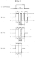
- Fig. 2 is a diagram for explaining a recording pulse waveform. It has been found that it is effective to increase or decrease the duty ratio of a multi-pulse portion (hereinafter to be referred to as an mp portion) in Fig. 2 at a recording linear velocity.
- the duty ratio refers to a time of a power level b of a low-level pulse in the mp portion divided by a time width of the mp portion.
- This information recording method has been particularly effective for an information recording medium that uses Ge, Ga, Sb, and Te as main components of the recording layer. This is because the thermal property of the recording layer that uses Ge, Ga, Sb, and Te as main components matches the recording pulse wave.
- Fig. 3 shows a recording waveform of a multi-speed recording at four times to ten times the recording velocity of a CD-RW as one example of the invention.
- This example also corresponds to a CAV recording of an inner periphery 4.8 m/s and an outer periphery 12.0 m/s.
- a duty ratio of the mp portion is decreased by matching duty ratios 0.625, 0.5, and 0.375 of the mp portion and an increase in the recording linear velocity, at the recording linear velocities 4.8, 9.6, and 12.0 m/s respectively.
- phase change type optical information recording medium that involves melting and rapid cooling of the recording layer, it is possible to obtain a balance between the melting and the cooling of the recording layer when the duty of the mp portion of the recording pulse is near 0.5. This is advantageous for various signal qualities and the overwriting.
- a recording linear velocity at which the duty ratio of the mp portion becomes 0.5 is larger than (a minimum recording linear velocity + a maximum recording linear velocity)/2 and equal to or less than the maximum recording linear velocity.
- a recording linear velocity that is often used in a drive that can achieve a multi-speed recording is a maximum recording linear velocity.
- a recording linear velocity becomes a high-speed recording at an outer periphery at which there is a large influence to a mechanical characteristic of the disk.
- the signal quality of a high-speed recording becomes more important in the CAV recording as well.
- it has been effective to set a recording pulse waveform having a duty ratio 0.5 of the mp portion with high reliability at a high-speed recording side.
- a recording linear velocity at which the duty ratio of the mp portion becomes 0.5 is larger than 0.55x (a minimum recording linear velocity + a maximum recording linear velocity) and less than the maximum recording linear velocity.
- Fig. 4 is a diagram for explaining an example of an apparatus for recording/reproducing information in the optical information recording medium according to the invention.
- the optical information recording medium is driven to rotate with driving means consisting of the spindle motor, and a light source consisting of a semiconductor laser is driven with a laser driving circuit as light-source driving means.
- a laser beam having a duty ratio of the mp portion increased or decreased at a recording linear velocity shown in Fig. 16 is irradiated onto an optical information recording medium via a not shown optical system from a semiconductor laser using a recording/reproducing pick-up.
- a phase change is generated on the recording layer of the optical information recording medium.
- a reflection beam from the optical information recording medium is received with the recording/reproducing pick-up, thereby to record/reproduce information onto/from the optical information recording medium.
- Optimum recording power of the recording/reproducing pick-up is set by a recording power setting circuit as a recording setting means.
- the apparatus for recording/reproducing information on/from the optical information recording medium generates a phase change in the recording layer of the optical information recording medium by irradiating a laser beam onto the optical information recording medium with the recording/reproducing pick-up, and carries out a recording/reproduction of information onto/from the optical information recording medium, and a rewriting of information.
- This recording/reproducing apparatus has recording means for recording information by modulating a signal to be recorded with a modulator, and recording this signal onto the optical information recording medium with the recording/reproducing pick-up.
- This recording means including this pick-up carries out a recording of information based on what is called a PWM recording system that records a mark to record a signal as a width of the mark onto a recording layer of the optical information recording medium.
- the recording means modulates the signal to be recorded with a modulator using a clock according to the EFM (Eight-to-Fourteen Modulation) system that is suitable for recording the information on a rewritable compact disk, or an improved modulation system of this system.
- EFM Eight-to-Fourteen Modulation
- a recording beam at the time of recording or rewriting a 0 signal having a signal width n ⁇ T after modulation (where n is a positive integer equal to or more than 1, and T represents a clock time, that is a time corresponding to a period of a clock used for modulating a signal) is a continuous beam having a power level e
- a recording beam pulse string at the time of recording or rewriting a 1 signal having a signal width nT after modulation is a laser wave pulse string that has a pulse portion fp having a time width x and a power level a, a multi-pulse portion mp in which a low-level pulse of a power level b having a time width T in total and a high-level pulse having a power level c alternately appear and continue by (n - n') times in total at a duty ratio y, and a pulse portion ep
- a polycarbonate substrate 31 of thickness 1.2 mm was used. Groove was formed on this substrate 31. This grove had a width 0.5 ⁇ m, and depth 35 nm.
- the first protection layer 32, recording layer 33, second protection layer 34, and the reflection layer 35 were formed on the substrate 31.
- the first and second protection layers 32 and 34 were made from ZnSSiO 2 .
- the first protection layer 32 has a thickness of 90 nm
- the second protection layer 34 has a thickness of 30 nm.
- the recording layer 33 was made from material having a composition shown in Table 1 to obtain Examples 1 to 6.
- the recording layer 33 had a thickness of 18 nm.
- the reflection layer 35 was made from an aluminum alloy.
- the reflection layer 6 had a thickness of 140 nm.
- the substrate 31 composition: polycarbonate
- first protection layer 32 composition: ZnS ⁇ SiO 2 , thickness: 90 nm
- recording layer 33 composition: as shown in Table 18, thickness: 18 nm
- second protection layer 34 composition: ZnS ⁇ SiO 2 , thickness: 30 nm
- the reflection layer 35 composition: Al alloy, thickness: 140 nm
- the overcoat layer 36 was formed on the reflection layer 35
- the hard coat layer 38 was formed on the other surface of the substrate 31 by spin coating an ultraviolet-ray-cured type resin to obtain a single-plate disk of the optical information recording medium.
- the print layer 37 was formed on the overcoat layer 36.
- this optical information recording medium was crystallized using an initializing unit having a large diameter LD.
- the phase change type optical information recording medium obtained based on the above method has been recorded with information at a recording linear velocity described in examples 1 to 6, and in a pulse wave having a duty rate of the mp portion shown in Table 1.
- An optical recording apparatus used in this example is similar to that shown in Fig. 4.
- the optical recording apparatus used has a pick-up having a wavelength 780 nm, and NA 0.5.
- a recording signal used has been an EFM-modulated input signal.
- As a result of reproducing at 1.2 m/s signals that have been recorded at respective linear velocities it has been possible to obtain satisfactory initial jitters of 22 ns, 20 ns, and 23 ns. After overwriting by 10,000 times at the respective recording linear velocities, it has been possible to obtain satisfactory jitters of 32 ns, 30 ns, and 33 ns.
- a preservation test on the optical information recording medium was carried out by leaving the disk for 500 hours in an environment at a temperature 80 °C and humidity 85%.
- the optical information recording medium did not show any signs of oxidization of the recording layer 33 or a change in the signal characteristics.
- the optical information recording medium can be preserved with great satisfaction for a long time.
- an optical information recording medium capable of recording at linear velocity that is higher than the even the maximum recording linear velocity of the optical information recording medium.
- optical information recording medium is according to the conventional technology or it is according to the present invention. Therefore, it is possible to provide an optical information recording medium capable of avoiding a recording on a conventional disk at a speed faster than a maximum recording linear velocity by error.
- optical information recording medium having good signal quality, excellent overwriting characteristic.
- optical information recording medium that is very reliable and can be mass-produced efficiently.
- optical information recordingmediumcapable of recording at a faster linear velocity than a maximum recording linear velocity, based on a fine adjustment of a currently-available general-purpose optical information recording apparatus.
- the method of recording/reproducing optical information it is decided whether it is possible or not to record at a recording linear velocity higher than a maximum recording linear velocity, and recording is carried out at a recording linear velocity higher than a maximum recording linear velocity, only when it is decided that it is possible to do so. Therefore, it is possible to provide an optical information recording medium and an optical information recording/reproducing method having no recording error.
- optical information recording medium that is excellent in power margin and that has satisfactory repetitive recording characteristic, recording and erasing sensitivities, and preservation characteristic. Moreover, when manufacturing the optical information recording medium, it is possible to efficiently form a recording layer having desired characteristics.
- an optical information recording medium that is capable of recording/erasing in a high linear velocity area (4.8 to 48 m/s) by using Ge, Ga, Sb, and Te as main constituent elements of the optical information recording medium, and specifying a film thickness and a composition of a recording layer, and that is excellent in total characteristics including reproduction stability and the life of a signal.
- an optical information recording medium with improved stability of reproducing a signal in a high-linear velocity area and improved life of a signal, by adding at least one element selected from a group consisting of In, Zn, Sn, Si, Pb, Co, Cr, Cu, Ag, Au, Pd, Pt, S, Se, Ta, Nb, V, Bi, Zr, Ti, Al, Mn, Mo, Rh, C, N, and O, to a recording layer that includes Ge, Ga, Sb, and Te as main constituent elements of the recording layer.
- an optical information recording medium that has a reflectivity that is necessary for initialization and recording/erasing in a high linear velocity area, by specifying a composition ratio of Sb to Te.
- an optical information recording medium that can achieve a high-linear velocity recording based on a general-purpose recording strategy, by specifying a film thickness of each layer of the optical information recording medium and a composition of a recording layer, and by specifying a time width of fp and ep and a duty ratio of mp, in a recording wave pulse string for recording or rewriting a signal, at the time of recording information onto the optical information recording medium according to a PWM recording system.
- an optical information recording medium capable of achieving a multi-speed recording or a CAV recording, by increasing or decreasing a duty ratio y of a pulse portion mp at a recording linear velocity, in a recording wave pulse string for recording or rewriting a signal, at the time of recording information onto the optical information recording medium according to a PWM recording system.
Landscapes
- Engineering & Computer Science (AREA)
- Physics & Mathematics (AREA)
- Optics & Photonics (AREA)
- Signal Processing (AREA)
- Manufacturing & Machinery (AREA)
- Chemical & Material Sciences (AREA)
- Inorganic Chemistry (AREA)
- Optical Record Carriers And Manufacture Thereof (AREA)
- Thermal Transfer Or Thermal Recording In General (AREA)
- Manufacturing Optical Record Carriers (AREA)
- Optical Recording Or Reproduction (AREA)
Claims (6)
- Optisches Informationsaufzeichnungsmedium umfassend
ein scheibenförmiges Substrat; und
mindestens eine auf das Substrat gestapelte Aufzeichnungsschicht vom Phasenänderungstyp, wobei die Aufzeichnungsschicht vom Phasenänderungstyp aus Material hergestellt ist, welches Ge, Ga, Sb und Te beinhaltet und, wenn α, β, γ und δ Atomprozentsätze von Ge, Ga, Sb und Te darstellen und α + β + γ + δ = 100 ist, α, β, γ und δ dann die Beziehungen erfüllen:


- Optisches Informationsaufzeichnungsmedium gemäß Anspruch 1, wobei der Aufzeichnungsschicht vom Phasenänderungstyp mindestens ein Element ausgewählt aus In, Zn, Sn, Si, Pb, Co, Cr, Cu, Ag, Au, Pd, Pt, S, Se, Ta, Nb, V, Bi, Zr, Ti, Al, Mn, Mo, Rh, C, N und O zugesetzt wurde.
- Optisches Informationsaufzeichnungsmedium gemäß Anspruch 1, wobei das Zusammensetzungsverhältnis von Ge und Ga -8 ≤ α - β ≤ 3 ist.
- Optisches Informationsaufzeichnungsmedium gemäß Anspruch 1, wobei das Zusammensetzungsverhältnis von Sb und Te γ + δ ≥ 88 ist.
- Verfahren zum Aufzeichnen/Wiedergeben von Information, um Information auf/aus dem optischen Informationsaufzeichnungsmedium gemäß irgendeinem der Ansprüche 1 bis 4 aufzuzeichnen, wiederzugeben und wieder zu beschreiben, welches Verfahren umfasst:Erzeugen einer Phasenänderung in einer Aufzeichnungsschicht des optischen Informationsaufzeichnungsmediums durch Einstrahlen eines Laserstrahls auf das optische Informationsaufzeichnungsmedium, undDurchführen einer Mehrgeschwindigkeits-Aufzeichnung und/oder einer CAV-Aufzeichnung auf dem optischen Informationsaufzeichnungsmedium, beruhend auf der Anordnung, dassim Fall der Aufzeichnung von Information auf das Informationsaufzeichnungsmedium durch Modulieren eines Signals gemäß dem PWM-Aufzeichnungssystem eine Aufzeichnungswelle zum Zeitpunkt der Aufzeichnung oder des Überschreibens eines 0-Signals mit einer Signalbreite n x T (wobei n eine positive ganze Zahl ≥1 ist und T eine Taktzeit ist) nach Modulation ein kontinuierlicher Strahl mit einem Energieniveau e ist, undeine Aufzeichnungswellen-Impulsfolge zum Zeitpunkt der Aufzeichnung oder des Überschreibens eines 1-Signals mit einer Signalbreite nT nach Modulation eine Impulsfolge elektromagnetischer Wellen ist, die einen Impulsteil fp mit einer Zeitbreite x und einem Energieniveau a, einen Mehrimpulsteil mp, in welchem ein Impuls niedrigen Niveaus von einem Energieniveau b mit einer Zeitbreite von insgesamt T und ein Impuls hohen Niveaus mit einem Energieniveau c bei einem Einschaltverhältnis y abwechselnd insgesamt (n-n') Mal fortlaufen, und einen Impulsteil ep mit einer Zeitbreite z und einem Energieniveau d aufweist, wobei die Zeitbreite x, das Einschaltverhältnis y und die Zeitbreite z die Bedingungen T x 0,5 ≤ x ≤ T x 2,0, 0,125 ≤ y ≤ 0,875 und T x 0,125 ≤ z ≤ T erfüllen, wobei n' eine positive ganze Zahl ≥ n ist, und die Energieniveaus a, b, c, d und e eine Beziehung a & c ≥ e ≥ b & d erfüllen.
- Verfahren zum Aufzeichnen/Wiedergeben von Information gemäß Anspruch 5, wobei das Einschaltverhältnis des Impulsteils mp gemäß der Lineargeschwindigkeit der Aufzeichnung zunimmt oder abnimmt.
Applications Claiming Priority (9)
| Application Number | Priority Date | Filing Date | Title |
|---|---|---|---|
| JP2000297364 | 2000-09-28 | ||
| JP2000297364 | 2000-09-28 | ||
| JP2000310536 | 2000-10-11 | ||
| JP2000310536 | 2000-10-11 | ||
| JP2000367361 | 2000-12-01 | ||
| JP2000367361 | 2000-12-01 | ||
| JP2001088516 | 2001-03-26 | ||
| JP2001088516 | 2001-03-26 | ||
| EP01123474A EP1193696B1 (de) | 2000-09-28 | 2001-09-28 | Optisches Aufzeichnungsmedium, Verfahren zu dessen Herstellung und Verfahren und Vorrichtung zum Aufzeichnen auf oder Lesen von diesem Medium |
Related Parent Applications (1)
| Application Number | Title | Priority Date | Filing Date |
|---|---|---|---|
| EP01123474A Division EP1193696B1 (de) | 2000-09-28 | 2001-09-28 | Optisches Aufzeichnungsmedium, Verfahren zu dessen Herstellung und Verfahren und Vorrichtung zum Aufzeichnen auf oder Lesen von diesem Medium |
Publications (2)
| Publication Number | Publication Date |
|---|---|
| EP1467351A1 EP1467351A1 (de) | 2004-10-13 |
| EP1467351B1 true EP1467351B1 (de) | 2007-01-10 |
Family
ID=27481659
Family Applications (3)
| Application Number | Title | Priority Date | Filing Date |
|---|---|---|---|
| EP01123474A Expired - Lifetime EP1193696B1 (de) | 2000-09-28 | 2001-09-28 | Optisches Aufzeichnungsmedium, Verfahren zu dessen Herstellung und Verfahren und Vorrichtung zum Aufzeichnen auf oder Lesen von diesem Medium |
| EP04014399A Expired - Lifetime EP1467352B1 (de) | 2000-09-28 | 2001-09-28 | Optisches Aufzeichnungsmedium, Verfahren zu dessen Herstellung und Verfahren und Vorrichtung zum Aufzeichnen auf oder Lesen von diesem Medium |
| EP04014398A Expired - Lifetime EP1467351B1 (de) | 2000-09-28 | 2001-09-28 | Optisches Aufzeichnungsmedium, Verfahren zu dessen Herstellung und Verfahren und Vorrichtung zum Aufzeichnen auf oder Lesen von diesem Medium |
Family Applications Before (2)
| Application Number | Title | Priority Date | Filing Date |
|---|---|---|---|
| EP01123474A Expired - Lifetime EP1193696B1 (de) | 2000-09-28 | 2001-09-28 | Optisches Aufzeichnungsmedium, Verfahren zu dessen Herstellung und Verfahren und Vorrichtung zum Aufzeichnen auf oder Lesen von diesem Medium |
| EP04014399A Expired - Lifetime EP1467352B1 (de) | 2000-09-28 | 2001-09-28 | Optisches Aufzeichnungsmedium, Verfahren zu dessen Herstellung und Verfahren und Vorrichtung zum Aufzeichnen auf oder Lesen von diesem Medium |
Country Status (4)
| Country | Link |
|---|---|
| US (1) | US7507523B2 (de) |
| EP (3) | EP1193696B1 (de) |
| JP (1) | JP4145036B2 (de) |
| DE (3) | DE60125993T2 (de) |
Families Citing this family (67)
| Publication number | Priority date | Publication date | Assignee | Title |
|---|---|---|---|---|
| US6600725B1 (en) * | 1998-12-16 | 2003-07-29 | At&T Corp. | Apparatus and method for providing multimedia conferencing services with selective information services |
| TW565835B (en) * | 2001-01-10 | 2003-12-11 | Ricoh Kk | Phase change optical recording medium |
| EP1229530A3 (de) * | 2001-02-01 | 2006-10-18 | Ricoh Company, Ltd. | Optisches Informationsaufzeichnungsmedium |
| US7027382B2 (en) | 2001-06-26 | 2006-04-11 | Ricoh Company, Ltd. | Optical recording medium having relation between reflection layer and pit lengths |
| WO2003034410A1 (fr) * | 2001-10-17 | 2003-04-24 | Tdk Corporation | Support d'enregistrement optique et procede pour enregistrer des informations sur un support d'enregistrement optique |
| US7164629B2 (en) | 2002-01-22 | 2007-01-16 | Ricoh Company, Ltd. | Method of controlling an optical disk apparatus |
| JP2003228834A (ja) | 2002-01-30 | 2003-08-15 | Ricoh Co Ltd | 情報記録方式及び光記録媒体 |
| CN1290106C (zh) * | 2002-03-07 | 2006-12-13 | 株式会社理光 | 光记录媒体及其制造方法 |
| JP3771859B2 (ja) | 2002-03-27 | 2006-04-26 | 株式会社リコー | 光情報記録方法及び光情報記録装置 |
| US7260053B2 (en) * | 2002-04-02 | 2007-08-21 | Ricoh Company, Ltd. | Optical recording medium, process for manufacturing the same, sputtering target for manufacturing the same, and optical recording process using the same |
| TWI254301B (en) * | 2002-04-05 | 2006-05-01 | Tdk Corp | Optical recording medium and method for optically recording information in the same |
| MXPA04010521A (es) * | 2002-04-24 | 2004-12-13 | Samsung Electronics Co Ltd | Medio optico de almacenamiento de informacion y metodo de grabacion sobre el mismo. |
| TWI254934B (en) * | 2002-04-26 | 2006-05-11 | Tdk Corp | Optical recording medium and method for optically recording data in the same |
| JP2003323717A (ja) * | 2002-05-02 | 2003-11-14 | Pioneer Electronic Corp | 情報記録再生装置および情報記録方法 |
| US7231649B2 (en) * | 2002-05-31 | 2007-06-12 | Tdk Corporation | Optical recording medium and method for optically recording data in the same |
| US20040038080A1 (en) * | 2002-07-01 | 2004-02-26 | Tdk Corporation | Optical recording medium and method for recording data in the same |
| JP4092147B2 (ja) * | 2002-07-04 | 2008-05-28 | Tdk株式会社 | 光記録媒体及び光記録方法 |
| DE60308958T2 (de) * | 2002-07-22 | 2007-03-15 | Ricoh Co., Ltd. | Optisches Phasenübergangsaufzeichnungsmedium |
| JP4282285B2 (ja) * | 2002-08-12 | 2009-06-17 | Tdk株式会社 | 光記録媒体及び光記録方法 |
| JP2004095034A (ja) * | 2002-08-30 | 2004-03-25 | Pioneer Electronic Corp | 情報記録媒体 |
| US7260044B2 (en) * | 2002-09-06 | 2007-08-21 | Ricoh Company, Ltd. | Recording method for a phase-change optical recording medium |
| US7063875B2 (en) * | 2002-09-13 | 2006-06-20 | Ricoh Company, Ltd. | Optical recording medium |
| US20040076907A1 (en) * | 2002-10-22 | 2004-04-22 | Tdk Corporation | Optical recording medium and method for manufacturing the same |
| US7351516B2 (en) * | 2002-11-06 | 2008-04-01 | Ricoh Company, Ltd. | Optical information recording medium |
| JP4249590B2 (ja) | 2002-11-18 | 2009-04-02 | 株式会社リコー | 光情報記録媒体およびその製造方法 |
| JP2004171642A (ja) * | 2002-11-19 | 2004-06-17 | Tdk Corp | 光記録媒体、光記録方法及び光記録装置 |
| US7781146B2 (en) * | 2002-11-22 | 2010-08-24 | Tdk Corporation | Optical recording medium |
| JP3996051B2 (ja) * | 2002-12-18 | 2007-10-24 | 株式会社リコー | 光記録方法 |
| US20040165523A1 (en) * | 2002-12-18 | 2004-08-26 | Akira Shimofuku | Optical recording medium with visible pattern formed in ROM area |
| JP3977740B2 (ja) * | 2002-12-27 | 2007-09-19 | 株式会社リコー | 相変化型光記録媒体とその記録方法 |
| US7932015B2 (en) | 2003-01-08 | 2011-04-26 | Tdk Corporation | Optical recording medium |
| TWI250515B (en) * | 2003-01-17 | 2006-03-01 | Ricoh Kk | Method of initializing phase change optical recording medium |
| JP4084674B2 (ja) * | 2003-01-28 | 2008-04-30 | Tdk株式会社 | 光記録媒体 |
| US7194750B2 (en) * | 2003-01-28 | 2007-03-20 | Ricoh Company, Ltd. | Recording/reproducing apparatus and disk cartridge |
| US6973451B2 (en) * | 2003-02-21 | 2005-12-06 | Sony Corporation | Medium content identification |
| JP2004255698A (ja) * | 2003-02-26 | 2004-09-16 | Victor Co Of Japan Ltd | 光記録媒体 |
| JP4611198B2 (ja) * | 2003-03-04 | 2011-01-12 | Jx日鉱日石金属株式会社 | 光情報記録媒体用の非晶質性保護膜を形成するためのスパッタリングターゲット、光情報記録媒体用の非晶質性保護膜及びその製造方法 |
| US20040202097A1 (en) * | 2003-04-08 | 2004-10-14 | Tdk Corporation | Optical recording disk |
| US7407698B2 (en) * | 2003-05-07 | 2008-08-05 | Ricoh Company, Ltd. | Flexible optical disk |
| JP2005025842A (ja) * | 2003-07-01 | 2005-01-27 | Tdk Corp | 光記録ディスク |
| JP2005025841A (ja) * | 2003-07-01 | 2005-01-27 | Tdk Corp | 光記録ディスク |
| JP2005022196A (ja) * | 2003-07-01 | 2005-01-27 | Tdk Corp | 光記録ディスク |
| JP2005044491A (ja) * | 2003-07-10 | 2005-02-17 | Ricoh Co Ltd | 光記録媒体およびその製造方法 |
| KR100889715B1 (ko) * | 2003-07-18 | 2009-03-23 | 미츠비시 가가쿠 메디아 가부시키가이샤 | 광기록 방법 |
| JP2005044438A (ja) * | 2003-07-22 | 2005-02-17 | Tdk Corp | 光記録ディスク |
| EP1515315B1 (de) | 2003-08-26 | 2007-07-25 | Ricoh Company, Ltd. | Informationsaufzeichnungsverfahren, Informationsaufzeichnungsvorrichtung, optisches Informationsaufzeichnungsmedium, Programm zur Aufzeichnung von Informationen und Speichermedium |
| EP1524656B1 (de) * | 2003-10-16 | 2009-09-16 | Ricoh Company, Ltd. | Medium zur optischen Datenspeicherung und Verfahren zu dessen Herstellung |
| JP2005129181A (ja) * | 2003-10-27 | 2005-05-19 | National Institute Of Advanced Industrial & Technology | 光記録ディスク |
| US7329361B2 (en) | 2003-10-29 | 2008-02-12 | International Business Machines Corporation | Method and apparatus for fabricating or altering microstructures using local chemical alterations |
| US7662689B2 (en) * | 2003-12-23 | 2010-02-16 | Intel Corporation | Strained transistor integration for CMOS |
| DE602004031775D1 (de) * | 2004-02-05 | 2011-04-21 | Ricoh Co Ltd | Phasenänderungsinformationsaufzeichnungsmedium, verfahren zu dessen herstellung und sputtertarget. |
| JP2005251265A (ja) * | 2004-03-02 | 2005-09-15 | Ricoh Co Ltd | 相変化型光記録媒体 |
| US20050221050A1 (en) * | 2004-03-19 | 2005-10-06 | Michiaki Shinotsuka | Two-layered optical recording medium, method for manufacturing the same, and, method and apparatus for optical recording and reproducing using the same |
| US20050238837A1 (en) * | 2004-04-26 | 2005-10-27 | Junichi Satou | Optical recording medium |
| US7767284B2 (en) * | 2004-04-28 | 2010-08-03 | Ricoh Company, Ltd. | Optical recording medium, and, method for manufacturing the same, and method and apparatus for optical recording and reproducing thereof |
| JP4382646B2 (ja) * | 2004-05-17 | 2009-12-16 | 株式会社リコー | 光記録媒体とその製造方法 |
| KR20070065915A (ko) | 2004-10-19 | 2007-06-25 | 코닌클리케 필립스 일렉트로닉스 엔.브이. | 광학 기록용 마스터 기판에 데이터 기록방법 |
| JP4248486B2 (ja) * | 2004-12-15 | 2009-04-02 | 株式会社リコー | 相変化型光記録媒体 |
| US20060174256A1 (en) * | 2005-02-03 | 2006-08-03 | Tohru Yashiro | Optical recording medium, production method thereof, and, method and apparatus for recording and reproducing optical recording medium |
| US20060210760A1 (en) * | 2005-03-17 | 2006-09-21 | Shinya Narumi | Phase change type optical information recording medium |
| EP1977420A4 (de) * | 2006-01-23 | 2009-08-26 | Ricoh Kk | Optisches aufzeichnungsmedium |
| JP5143129B2 (ja) * | 2006-05-09 | 2013-02-13 | コーニンクレッカ フィリップス エレクトロニクス エヌ ヴィ | ディスクをアクセスするための方法及び装置 |
| EP2339578A1 (de) * | 2006-06-12 | 2011-06-29 | Panasonic Corporation | Lesevorrichtung und Leseverfahren für ein optisches Datenaufzeichnungsmedium |
| JP2008276900A (ja) * | 2007-04-02 | 2008-11-13 | Ricoh Co Ltd | 追記型光記録媒体 |
| US20100068529A1 (en) * | 2008-09-12 | 2010-03-18 | Asplund Matthew C | Films containing an infused oxygenated as and methods for their preparation |
| AU2009292148A1 (en) * | 2008-09-12 | 2010-03-18 | Brigham Young University | Data storage media containing carbon and metal layers |
| CA2759927C (en) | 2009-04-22 | 2017-10-24 | Franwell, Inc. | A wearable rfid system |
Family Cites Families (65)
| Publication number | Priority date | Publication date | Assignee | Title |
|---|---|---|---|---|
| JP3124720B2 (ja) | 1995-04-14 | 2001-01-15 | 株式会社リコー | 情報記録再生方法、情報記録再生装置及び情報記録媒体 |
| US3530441A (en) | 1969-01-15 | 1970-09-22 | Energy Conversion Devices Inc | Method and apparatus for storing and retrieving information |
| JPS60177446A (ja) | 1984-02-23 | 1985-09-11 | Nippon Telegr & Teleph Corp <Ntt> | 光デイスク記録媒体 |
| JPS61219692A (ja) | 1985-03-26 | 1986-09-30 | Matsushita Electric Ind Co Ltd | 光学情報記録部材 |
| JPS61270190A (ja) | 1985-05-24 | 1986-11-29 | Matsushita Electric Ind Co Ltd | 光学情報記録部材 |
| JPH0673991B2 (ja) | 1985-07-18 | 1994-09-21 | 松下電器産業株式会社 | 光学情報記録素子 |
| JPS6273438A (ja) | 1985-09-25 | 1987-04-04 | Matsushita Electric Ind Co Ltd | 光学情報記録部材 |
| JPS61239428A (ja) | 1986-02-21 | 1986-10-24 | Canon Inc | 信号記録方式 |
| JP2629696B2 (ja) | 1987-03-17 | 1997-07-09 | 松下電器産業株式会社 | 光学情報記録再生消去部材 |
| JPS63251290A (ja) | 1987-04-08 | 1988-10-18 | Hitachi Ltd | 光記録媒体と記録・再生方法及びその応用 |
| JPS63261552A (ja) * | 1987-04-18 | 1988-10-28 | Fujitsu Ltd | 光学的情報記録媒体の製造法 |
| JPS63266633A (ja) | 1987-04-23 | 1988-11-02 | Fuji Photo Film Co Ltd | 光情報記録方法 |
| JP2702923B2 (ja) | 1987-04-24 | 1998-01-26 | 株式会社日立製作所 | 情報の記録方法及び情報記録装置 |
| DE3885156T2 (de) * | 1987-06-11 | 1994-03-17 | Asahi Chemical Ind | Verfahren zum Aufzeichnen und Löschen von Daten. |
| JPH01277338A (ja) | 1988-04-28 | 1989-11-07 | Nippon Telegr & Teleph Corp <Ntt> | 光記録媒体 |
| JPH01303643A (ja) | 1988-06-01 | 1989-12-07 | Nippon Telegr & Teleph Corp <Ntt> | レーザ記録媒体 |
| JP2941848B2 (ja) | 1988-07-20 | 1999-08-30 | 株式会社リコー | 光記録媒体 |
| US5150351A (en) | 1989-06-30 | 1992-09-22 | Matsushita Electric Industrial Co., Ltd. | Optical information recording apparatus for recording an input signal having variable width pulse duration and pulse spacing periods |
| US5156693A (en) * | 1990-02-19 | 1992-10-20 | Ricoh Company, Ltd. | Information recording medium |
| JP2868849B2 (ja) | 1990-02-19 | 1999-03-10 | 株式会社リコー | 情報記録媒体 |
| JP3032585B2 (ja) | 1990-12-28 | 2000-04-17 | 株式会社リコー | 情報記録媒体 |
| JP3058443B2 (ja) | 1990-11-27 | 2000-07-04 | 株式会社リコー | 光情報記録媒体 |
| JPH03297689A (ja) * | 1990-04-17 | 1991-12-27 | Toray Ind Inc | 情報記録媒体 |
| JP3136153B2 (ja) | 1990-06-19 | 2001-02-19 | 松下電器産業株式会社 | 光記録媒体及びその製造方法 |
| JP3078823B2 (ja) | 1990-06-19 | 2000-08-21 | 松下電器産業株式会社 | 光記録媒体及びその製造方法 |
| JPH04123551A (ja) | 1990-09-14 | 1992-04-23 | Toshiba Corp | 正弦波合成回路 |
| JPH04163839A (ja) | 1990-10-26 | 1992-06-09 | Nec Kagoshima Ltd | 蛍光表示管 |
| JP3032600B2 (ja) | 1991-02-21 | 2000-04-17 | 株式会社リコー | 光情報記録媒体 |
| JP3267675B2 (ja) | 1991-06-04 | 2002-03-18 | 株式会社リコー | 光情報記録媒体及びその製造方法 |
| JPH06166268A (ja) | 1992-07-09 | 1994-06-14 | Ricoh Co Ltd | 光情報記録媒体およびその製造方法 |
| JP2751089B2 (ja) | 1992-11-30 | 1998-05-18 | 大日本インキ化学工業株式会社 | レーザーマーキング方法及び印刷インキ |
| JPH06330308A (ja) * | 1993-05-20 | 1994-11-29 | Canon Inc | スパッタリング方法、光記録媒体の製造方法および光記録媒体 |
| US5785828A (en) * | 1994-12-13 | 1998-07-28 | Ricoh Company, Ltd. | Sputtering target for producing optical recording medium |
| JP2990036B2 (ja) * | 1995-02-13 | 1999-12-13 | ティーディーケイ株式会社 | 光記録媒体およびその製造方法 |
| US6319368B1 (en) | 1995-03-31 | 2001-11-20 | Ricoh Company, Ltd. | Sputtering target, method of producing the target, optical recording medium fabricated by using the sputtering target, and method of forming recording layer for the optical recording medium |
| US5736657A (en) * | 1995-03-31 | 1998-04-07 | Ricoh Company, Ltd. | Sputtering target |
| JP3081551B2 (ja) | 1995-04-14 | 2000-08-28 | 株式会社リコー | 情報記録再生方法 |
| JP3124721B2 (ja) | 1995-09-11 | 2001-01-15 | 株式会社リコー | 光学的情報記録再生方法及び光学的情報記録再生装置 |
| BE1009677A3 (nl) * | 1995-09-29 | 1997-06-03 | Philips Electronics Nv | Informatiedrager en inrichting voor het beschrijven van een informatiedrager. |
| JP3525197B2 (ja) | 1996-02-27 | 2004-05-10 | 株式会社リコー | 相変化型光記録媒体 |
| JPH1064128A (ja) * | 1996-04-25 | 1998-03-06 | Toray Ind Inc | 光記録媒体およびその製造方法 |
| DE69738285T2 (de) * | 1996-09-06 | 2008-02-28 | Ricoh Co., Ltd. | Optisches Speichermedium |
| JPH10326438A (ja) * | 1997-05-26 | 1998-12-08 | Tdk Corp | 光記録媒体の製造方法および光記録媒体 |
| SG72852A1 (en) | 1997-08-15 | 2000-05-23 | Ricoh Kk | Optical recording medium and recording and reproducing method using the same |
| JP3782223B2 (ja) | 1997-08-15 | 2006-06-07 | 株式会社リコー | 光記録媒体及びこれの記録再生方法 |
| US6096398A (en) * | 1997-11-28 | 2000-08-01 | Ricoh Company, Ltd. | Phase-change optical recording medium |
| US6177167B1 (en) | 1997-12-02 | 2001-01-23 | Ricoh Company, Ltd. | Optical information recording medium |
| JP2000067435A (ja) * | 1997-12-27 | 2000-03-03 | Tdk Corp | 光記録媒体およびその記録方法 |
| JPH11213628A (ja) * | 1998-01-21 | 1999-08-06 | Toshiba Corp | 記録媒体とその再生装置および記録再生装置 |
| US6426936B1 (en) | 1998-01-27 | 2002-07-30 | Ricoh Company, Ltd. | Phase-change medium usable in phase-difference tracking |
| EP2280398A3 (de) * | 1998-02-23 | 2011-03-09 | Kabushiki Kaisha Toshiba | Informationsaufzeichnungsmedium, Informationswiedergabeverfahren und -vorrichtung, und Informationsaufzeichnungsverfahren |
| US6477135B1 (en) * | 1998-03-26 | 2002-11-05 | Matsushita Electric Industrial Co., Ltd. | Optical information recording medium and method for recording and reproduction information thereon |
| JP3419347B2 (ja) * | 1998-07-01 | 2003-06-23 | 三菱化学株式会社 | 光学的情報記録用媒体、記録方法及び光学的情報記録用媒体の製造方法 |
| JP2000182274A (ja) * | 1998-10-06 | 2000-06-30 | Tdk Corp | 光記録媒体および光記録方法 |
| US6352753B2 (en) * | 1998-11-10 | 2002-03-05 | Toray Industries, Inc. | Optical recording medium |
| JP2000195112A (ja) | 1998-12-24 | 2000-07-14 | Ricoh Co Ltd | 相変化型情報記録媒体の初期化方法 |
| US6511788B1 (en) * | 1999-02-12 | 2003-01-28 | Sony Corporation | Multi-layered optical disc |
| JP2000322740A (ja) | 1999-05-12 | 2000-11-24 | Ricoh Co Ltd | 光記録媒体及びその記録方法 |
| DE60027815T2 (de) * | 1999-05-19 | 2006-12-21 | Mitsubishi Kagaku Media Corp., Ltd. | Wiederbeschreibbares optisches Aufzeichnungsmedium und optisches Aufzeichnungsverfahren |
| JP2000339751A (ja) * | 1999-06-01 | 2000-12-08 | Ricoh Co Ltd | 相変化形光記録媒体 |
| US6479121B1 (en) | 1999-09-21 | 2002-11-12 | Ricoh Company, Ltd. | Optical recording medium and method of fabricating same |
| JP2001101660A (ja) | 1999-09-27 | 2001-04-13 | Ricoh Co Ltd | 光記録媒体及び光記録媒体の記録方法 |
| JP4112153B2 (ja) | 2000-03-31 | 2008-07-02 | 株式会社リコー | 光記録媒体の検査方法 |
| US6487121B1 (en) * | 2000-08-25 | 2002-11-26 | Advanced Micro Devices, Inc. | Method of programming a non-volatile memory cell using a vertical electric field |
| US7027382B2 (en) * | 2001-06-26 | 2006-04-11 | Ricoh Company, Ltd. | Optical recording medium having relation between reflection layer and pit lengths |
-
2001
- 2001-09-28 EP EP01123474A patent/EP1193696B1/de not_active Expired - Lifetime
- 2001-09-28 DE DE60125993T patent/DE60125993T2/de not_active Expired - Lifetime
- 2001-09-28 EP EP04014399A patent/EP1467352B1/de not_active Expired - Lifetime
- 2001-09-28 DE DE60132380T patent/DE60132380T2/de not_active Expired - Lifetime
- 2001-09-28 DE DE60125675T patent/DE60125675T2/de not_active Expired - Lifetime
- 2001-09-28 US US09/966,171 patent/US7507523B2/en not_active Expired - Fee Related
- 2001-09-28 JP JP2001304019A patent/JP4145036B2/ja not_active Expired - Fee Related
- 2001-09-28 EP EP04014398A patent/EP1467351B1/de not_active Expired - Lifetime
Also Published As
| Publication number | Publication date |
|---|---|
| EP1193696A3 (de) | 2003-07-16 |
| DE60125675D1 (de) | 2007-02-15 |
| DE60125993T2 (de) | 2007-10-18 |
| DE60132380T2 (de) | 2009-01-02 |
| EP1467352A1 (de) | 2004-10-13 |
| EP1193696B1 (de) | 2007-01-03 |
| JP4145036B2 (ja) | 2008-09-03 |
| US7507523B2 (en) | 2009-03-24 |
| DE60125993D1 (de) | 2007-02-22 |
| EP1193696A2 (de) | 2002-04-03 |
| US20020110063A1 (en) | 2002-08-15 |
| DE60132380D1 (de) | 2008-02-21 |
| EP1467352B1 (de) | 2008-01-09 |
| JP2002358691A (ja) | 2002-12-13 |
| EP1467351A1 (de) | 2004-10-13 |
| DE60125675T2 (de) | 2007-10-11 |
Similar Documents
| Publication | Publication Date | Title |
|---|---|---|
| EP1467351B1 (de) | Optisches Aufzeichnungsmedium, Verfahren zu dessen Herstellung und Verfahren und Vorrichtung zum Aufzeichnen auf oder Lesen von diesem Medium | |
| JP3839213B2 (ja) | 相変化型光記録媒体の記録方法および記録再生装置 | |
| US6280810B1 (en) | Phase-change information recording medium and optical recording method to make higher rotation rates feasible | |
| EP1248253B1 (de) | Optisches Informationsaufzeichnungsmedium, Informationsaufzeichnungsverfahren, und dieses Aufzeichnungsmedium benutzendes Gerät | |
| EP1378894A2 (de) | Optischer Aufzeichnungsträger und Verfahren um Daten darin aufzuzeichnen | |
| EP1381033B1 (de) | Optisches Informationsaufzeichnungsmedium, Verfahren zur Festellung der Aufzeichnungsbedingung, optisches Informationsaufzeichnungsgerät und Informationsverarbeitungsgerät | |
| EP1434206B1 (de) | Optisches Aufzeichnungsmedium vom Phasenwechseltyp und Aufzeichnungsverfahren dafür | |
| JP2006044215A (ja) | 光記録媒体及びその製造方法、スパッタリングターゲット、並びに光記録媒体の使用方法及び光記録装置 | |
| JP4234913B2 (ja) | 光情報記録媒体 | |
| JP3790673B2 (ja) | 光記録方法、光記録装置および光記録媒体 | |
| EP0846322B1 (de) | Reversibles optisches informationsmedium | |
| JP2002264515A (ja) | 光記録媒体および情報記録再生方法 | |
| JP3847151B2 (ja) | 相変化型光情報記録媒体の記録方法及び記録装置 | |
| JP3821695B2 (ja) | 光情報記録媒体への記録方法および記録装置 | |
| JP2002225437A (ja) | 光記録媒体 | |
| JP2002092889A (ja) | 相変化記録光ディスクのダイレクトオーバーライト方法及び情報記録再生装置 | |
| EP1515313A1 (de) | Verfahren zum aufzeichnen von daten auf einem optischen aufzeichnungsmedium, einrichtung zum aufzeichnen von daten auf einem optischen aufzeichnungsmedium und optisches aufzeichnungsmedium | |
| JP2001184651A (ja) | 相変化型情報記録媒体およびその記録方法 | |
| EP1511014A1 (de) | Aufzeichnungsverfahren für ein optisches aufzeichnungsmedium, datenrecorder für ein optisches aufzeichnungsmedium und optisches aufzeichnungsmedium | |
| JP2005093012A (ja) | 相変化型光情報記録媒体 | |
| JP2004095087A (ja) | 光記録媒体、その記録方法および記録装置 | |
| JP2003157536A (ja) | 光情報記録媒体への記録方法及び装置 | |
| JP2003228847A (ja) | 相変化型光ディスクの記録方法 | |
| JP2003285558A (ja) | 相変化型光記録媒体 | |
| JP2002269838A (ja) | 検査用光記録媒体、検査用光記録媒体の製造方法及びディスクドライブ検査方法 |
Legal Events
| Date | Code | Title | Description |
|---|---|---|---|
| PUAI | Public reference made under article 153(3) epc to a published international application that has entered the european phase |
Free format text: ORIGINAL CODE: 0009012 |
|
| AC | Divisional application: reference to earlier application |
Ref document number: 1193696 Country of ref document: EP Kind code of ref document: P |
|
| AK | Designated contracting states |
Kind code of ref document: A1 Designated state(s): DE FR GB |
|
| 17P | Request for examination filed |
Effective date: 20041217 |
|
| 17Q | First examination report despatched |
Effective date: 20050301 |
|
| AKX | Designation fees paid |
Designated state(s): DE FR GB |
|
| GRAP | Despatch of communication of intention to grant a patent |
Free format text: ORIGINAL CODE: EPIDOSNIGR1 |
|
| GRAS | Grant fee paid |
Free format text: ORIGINAL CODE: EPIDOSNIGR3 |
|
| GRAA | (expected) grant |
Free format text: ORIGINAL CODE: 0009210 |
|
| AC | Divisional application: reference to earlier application |
Ref document number: 1193696 Country of ref document: EP Kind code of ref document: P |
|
| AK | Designated contracting states |
Kind code of ref document: B1 Designated state(s): DE FR GB |
|
| REG | Reference to a national code |
Ref country code: GB Ref legal event code: FG4D |
|
| REF | Corresponds to: |
Ref document number: 60125993 Country of ref document: DE Date of ref document: 20070222 Kind code of ref document: P |
|
| ET | Fr: translation filed | ||
| PLBE | No opposition filed within time limit |
Free format text: ORIGINAL CODE: 0009261 |
|
| STAA | Information on the status of an ep patent application or granted ep patent |
Free format text: STATUS: NO OPPOSITION FILED WITHIN TIME LIMIT |
|
| 26N | No opposition filed |
Effective date: 20071011 |
|
| REG | Reference to a national code |
Ref country code: DE Ref legal event code: R082 Ref document number: 60125993 Country of ref document: DE Representative=s name: MEISSNER, BOLTE & PARTNER GBR, DE Ref country code: DE Ref legal event code: R082 Ref document number: 60125993 Country of ref document: DE Representative=s name: MEISSNER BOLTE PATENTANWAELTE RECHTSANWAELTE P, DE |
|
| REG | Reference to a national code |
Ref country code: DE Ref legal event code: R082 Ref document number: 60125993 Country of ref document: DE Representative=s name: MEISSNER, BOLTE & PARTNER GBR, DE |
|
| REG | Reference to a national code |
Ref country code: FR Ref legal event code: PLFP Year of fee payment: 16 |
|
| REG | Reference to a national code |
Ref country code: FR Ref legal event code: PLFP Year of fee payment: 17 |
|
| REG | Reference to a national code |
Ref country code: FR Ref legal event code: PLFP Year of fee payment: 18 |
|
| PGFP | Annual fee paid to national office [announced via postgrant information from national office to epo] |
Ref country code: DE Payment date: 20190918 Year of fee payment: 19 Ref country code: FR Payment date: 20190925 Year of fee payment: 19 |
|
| PGFP | Annual fee paid to national office [announced via postgrant information from national office to epo] |
Ref country code: GB Payment date: 20190920 Year of fee payment: 19 |
|
| REG | Reference to a national code |
Ref country code: DE Ref legal event code: R119 Ref document number: 60125993 Country of ref document: DE |
|
| GBPC | Gb: european patent ceased through non-payment of renewal fee |
Effective date: 20200928 |
|
| PG25 | Lapsed in a contracting state [announced via postgrant information from national office to epo] |
Ref country code: FR Free format text: LAPSE BECAUSE OF NON-PAYMENT OF DUE FEES Effective date: 20200930 Ref country code: DE Free format text: LAPSE BECAUSE OF NON-PAYMENT OF DUE FEES Effective date: 20210401 |
|
| PG25 | Lapsed in a contracting state [announced via postgrant information from national office to epo] |
Ref country code: GB Free format text: LAPSE BECAUSE OF NON-PAYMENT OF DUE FEES Effective date: 20200928 |