EP1484802A2 - Optische Halbleitervorrichtung - Google Patents
Optische Halbleitervorrichtung Download PDFInfo
- Publication number
- EP1484802A2 EP1484802A2 EP03023836A EP03023836A EP1484802A2 EP 1484802 A2 EP1484802 A2 EP 1484802A2 EP 03023836 A EP03023836 A EP 03023836A EP 03023836 A EP03023836 A EP 03023836A EP 1484802 A2 EP1484802 A2 EP 1484802A2
- Authority
- EP
- European Patent Office
- Prior art keywords
- optical semiconductor
- soft resin
- semiconductor chip
- resin
- aperture
- Prior art date
- Legal status (The legal status is an assumption and is not a legal conclusion. Google has not performed a legal analysis and makes no representation as to the accuracy of the status listed.)
- Granted
Links
Images


Classifications
-
- H—ELECTRICITY
- H10—SEMICONDUCTOR DEVICES; ELECTRIC SOLID-STATE DEVICES NOT OTHERWISE PROVIDED FOR
- H10H—INORGANIC LIGHT-EMITTING SEMICONDUCTOR DEVICES HAVING POTENTIAL BARRIERS
- H10H20/00—Individual inorganic light-emitting semiconductor devices having potential barriers, e.g. light-emitting diodes [LED]
- H10H20/80—Constructional details
- H10H20/85—Packages
- H10H20/855—Optical field-shaping means, e.g. lenses
-
- H—ELECTRICITY
- H10—SEMICONDUCTOR DEVICES; ELECTRIC SOLID-STATE DEVICES NOT OTHERWISE PROVIDED FOR
- H10H—INORGANIC LIGHT-EMITTING SEMICONDUCTOR DEVICES HAVING POTENTIAL BARRIERS
- H10H20/00—Individual inorganic light-emitting semiconductor devices having potential barriers, e.g. light-emitting diodes [LED]
- H10H20/80—Constructional details
- H10H20/85—Packages
- H10H20/852—Encapsulations
- H10H20/853—Encapsulations characterised by their shape
-
- H—ELECTRICITY
- H10—SEMICONDUCTOR DEVICES; ELECTRIC SOLID-STATE DEVICES NOT OTHERWISE PROVIDED FOR
- H10H—INORGANIC LIGHT-EMITTING SEMICONDUCTOR DEVICES HAVING POTENTIAL BARRIERS
- H10H20/00—Individual inorganic light-emitting semiconductor devices having potential barriers, e.g. light-emitting diodes [LED]
- H10H20/80—Constructional details
- H10H20/85—Packages
- H10H20/852—Encapsulations
- H10H20/854—Encapsulations characterised by their material, e.g. epoxy or silicone resins
-
- H—ELECTRICITY
- H10—SEMICONDUCTOR DEVICES; ELECTRIC SOLID-STATE DEVICES NOT OTHERWISE PROVIDED FOR
- H10W—GENERIC PACKAGES, INTERCONNECTIONS, CONNECTORS OR OTHER CONSTRUCTIONAL DETAILS OF DEVICES COVERED BY CLASS H10
- H10W72/00—Interconnections or connectors in packages
- H10W72/50—Bond wires
- H10W72/531—Shapes of wire connectors
- H10W72/536—Shapes of wire connectors the connected ends being ball-shaped
-
- H—ELECTRICITY
- H10—SEMICONDUCTOR DEVICES; ELECTRIC SOLID-STATE DEVICES NOT OTHERWISE PROVIDED FOR
- H10W—GENERIC PACKAGES, INTERCONNECTIONS, CONNECTORS OR OTHER CONSTRUCTIONAL DETAILS OF DEVICES COVERED BY CLASS H10
- H10W72/00—Interconnections or connectors in packages
- H10W72/50—Bond wires
- H10W72/531—Shapes of wire connectors
- H10W72/5363—Shapes of wire connectors the connected ends being wedge-shaped
-
- H—ELECTRICITY
- H10—SEMICONDUCTOR DEVICES; ELECTRIC SOLID-STATE DEVICES NOT OTHERWISE PROVIDED FOR
- H10W—GENERIC PACKAGES, INTERCONNECTIONS, CONNECTORS OR OTHER CONSTRUCTIONAL DETAILS OF DEVICES COVERED BY CLASS H10
- H10W72/00—Interconnections or connectors in packages
- H10W72/50—Bond wires
- H10W72/551—Materials of bond wires
- H10W72/552—Materials of bond wires comprising metals or metalloids, e.g. silver
- H10W72/5522—Materials of bond wires comprising metals or metalloids, e.g. silver comprising gold [Au]
-
- H—ELECTRICITY
- H10—SEMICONDUCTOR DEVICES; ELECTRIC SOLID-STATE DEVICES NOT OTHERWISE PROVIDED FOR
- H10W—GENERIC PACKAGES, INTERCONNECTIONS, CONNECTORS OR OTHER CONSTRUCTIONAL DETAILS OF DEVICES COVERED BY CLASS H10
- H10W90/00—Package configurations
- H10W90/701—Package configurations characterised by the relative positions of pads or connectors relative to package parts
- H10W90/751—Package configurations characterised by the relative positions of pads or connectors relative to package parts of bond wires
- H10W90/756—Package configurations characterised by the relative positions of pads or connectors relative to package parts of bond wires between a chip and a stacked lead frame, conducting package substrate or heat sink
Definitions
- the present invention relates to an optical semiconductor device using an optical semiconductor chip such as an LED lamp. More particularly, it has an object to provide a structure capable of preventing a semiconductor chip to be damaged from variations in environmental temperature to improve reliability and preventing performance to be deteriorated due to the improved reliability to allow the reliability and the performance to exist together.
- an optical semiconductor chip is sealed in a f irst, relatively soft resinous member to improve resistances against shock and moisture. Further, the first resinous member is sealed in a second, relatively hard resinous member to improve the mechanical strength. In this way, two resins with different characteristics can be employed together to compensate for a function lacked in one from another to improve the reliability. (See Patent Publication 1: JP-A-05/327029, paragraphs 5-7, Fig. 1, for example).
- the relatively soft resin is commonly selected as the inner resin that directly contacts the optical semiconductor chip and the relatively hard resin as the outer resin to achieve the required mechanical strength.
- a space B is provided between a soft resin 91 and a hard resin 92. This space is effective to prevent a compressive stress to be imposed on an optical semiconductor 93 even if a volume expansion occurs in the soft resin 91 as an environmental temperature elevates.
- the light emitted from (or coming into) the optical semiconductor chip 93 always passes through thespaceB, thatis, airthathasalowerrefractiveindexcompared to the resin.
- reflection occurred at an interface between the resin and the air causes a loss in amount of light, resulting in an output reduction of about 25-35%.
- Such the output reduction causes a problem associate with deterioration of the performance as the optical semiconductor device.
- the holder 94 commonly employs a lead-frame-insert injection-molded product in its structure.
- an air layer is interposed between the frame and the insert-molded product.
- the air layer expands under a high-temperature ambient and applies pressure to the soft resin, which produces bubbles therein.
- the production of bubbles causes a problem because it lowers the optical output similar to the above case and deteriorates the performance as the optical semiconductor device.
- the present invention provides an optical semiconductor device, which comprises an optical semiconductor chip sealed in a surrounding soft resin; a holder formed around the soft resin and integrally with a lead frame; and a covering lens composed of a transparent resin harder than the soft resin.
- the holder has an aperture configured to relieve a state of hermetic sealing for the soft resin and formed in a direction that imposes no optical influence on a function of the optical semiconductor chip.
- the lead frame may protrude into the aperture of the holder so as to occupy an inner rim of the aperture at a ratio below 1/2 in length.
- the reference numeral 1 denotes an optical semiconductor device according to the present invention.
- the optical semiconductor device 1 comprises an optical semiconductor chip 2, which is double sealed in a relatively softer soft resin 3 and in a relatively harder hard resin 4 as is in the art.
- the optical semiconductor chip 2 is entirely surrounded by the soft resin 3 and blocked from air to prevent the optical semiconductor chip 2 to be deteriorated from moisture in the atmosphere.
- the optical semiconductor chip 2 is wired through a fine-diameter gold wire 5. Accordingly, it is covered in the soft resin 3 to prevent the gold wire 5 to be broken or peeled from the optical semiconductor chip 2 due to vibrations.
- the optical semiconductor chip 2 thus covered in the soft resin 3 is further covered from external by the hard resin 4 to improve the mechanical strength, which prevents deformation of the soft resin 3 due to external stress and further ensures the improvement of reliability.
- the hard resin 4 has a characteristic for reinforcing weaknesses in the soft resin 3 such as a chemical resistance to improve the reliability on other points than the external stress.
- the present invention provides an aperture as a means for avoiding an excessive elevation in compressive stress imposed on the optical semiconductor chip 2 caused at a high temperature by a difference in expansion coefficient between the soft resin 3 and the hard resin 4. If the optical semiconductor chip 2 is a light-emitting element, the aperture is provided at a location that is not involved in an optical path for a light emitted from the optical semiconductor chip 2. If the optical semiconductor chip 2 is a photo-detecting element, the aperture is provided at a location that is not involved in an optical path for an external light coming into the optical semiconductor chip 2.
- the part composed of the hard resin 4 is divided into a lens 6 and a holder 7, which are formed previously.
- the holder 7 is provided with a lead frame 8 for mounting the optical semiconductor chip 2 thereon.
- the optical semiconductor chip 2 is mounted on the lead frame 8 integrally formed with the holder 7 and wired via the gold wire 5.
- the holder 7 is provided with an aperture 7a for mounting the optical semiconductor chip 2, which is formed in the front side, or the side to be combined with the lens 6 as described later.
- Another aperture 7b is formed in the rear side for relieving the compressive stress imposed on the optical semiconductor chip 2.
- the holder 7 is coupled to the lens 6 using an appropriate coupling means such as a hook structure. Accordingly, the aperture 7a provided in front of the optical semiconductor chip 2 is closed by the lens 6, and only the aperture 7b provided at the rear side remains open.
- the soft resin 3 such as a silicone resin is injected through the aperture 7b and, after degassing, heated to achieve an appropriate hardness.
- the processes produce the construction of the present invention. It comprises the soft resin 3 formed to surround the whole optical semiconductor chip 2 and the hard resin 4 (the lens 6 and the holder 7) formed to surround the soft resin 3 except for the aperture 7b where the optical semiconductor chip 2 does not function.
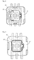
- Fig. 3 shows a layout of the holder 7 of the present invention.
- the reference numeral 21 denotes a holder, 22 a lead frame, and 23 an aperture.
- the lead frame 22 protrudes into the aperture 23 in the holder 21 so as to occupy an inner rim of the aperture 23 at a ratio below 1/2 in length of the inner rim of the aperture 23.
- the lead frame 22 is so formed by appropriately shaping the part sealed in the holder 21 and the part protruded into the aperture 23.
- Fig. 4 shows a reference example, in which a lead frame almost entirely contacts the whole rim of an aperture in a molded holder.
- the reference numeral 21' denoted a holder, 22' a lead frame, and 23' an aperture.
- the inner rim of the holder 21, which forms the aperture 23 includes portions (parts of the bold line in Fig. 3) where the lead frame 22 contacts the inner wall of the holder 21. Reducing such the portions as small as possible is effective to reduce an interface between the lead frame 22 and the holder 21 to prevent production of bubbles. The effect can be confirmed when the lead frame 22 partly contacts the inner wall of the holder in length in the circumferential direction at a ratio below about 1/2 the length of the inner rim in the holder 21 shown in Fig. 3.
- the optical semiconductor chip 2 is entirely surrounded by and sealed in the soft resin 3 such as a silicone resin for blocking the atmosphere to prevent deterioration due to moistures and toxic gases.
- the soft resin 3 is flexible sufficient to protect the optical semiconductor chip 2 from external vibrations.
- the hard resin 4 (the lens 6 and the holder 7) is provided with the aperture 7b as described above and accordingly is not configured to hermetically seal the soft resin 3. Therefore, even if the soft resin 3 has a larger thermal expansion coefficient, an extra volume of the soft resin 3 caused from the environmental temperature increase can extend through the aperture 7b and imposes no pressure elevation on the optical semiconductor chip 2.
- the inner rim of the holder 21, which forms the aperture 23 includes portions (parts of the bold line in Fig. 3) where the lead frame 22 contacts the inner wall of the holder 21. Reducing such the portions as small as possible is effective to reduce an interface between the lead frame 22 and the holder 21 to prevent production of bubbles.
- the reduced area of the lead frame 22 in the aperture 23 has an accompanying effect on reduction of a flow resistance against the soft resin injection and relaxation of damage suffered by the gold wire and the optical semiconductor chip 2.
- the optical semiconductor device comprises an optical semiconductor chip sealed in a surrounding soft resin; a holder composed of a hard resin harder than the soft resin and formed around the soft resin and integrally with a lead frame; and a covering lens composed of a transparent resin.
- the holder has an aperture configured to relieve a state of hermetic sealing for the soft resin and formed in a direction that imposes no optical influence on a function of the optical semiconductor chip.
- the lead frame protrudes into the aperture of the holder so as to occupy an inner rim of the aperture at a ratio below 1/2 in length. Therefore, on formation of a highly reliable optical semiconductor device double sealed with soft and hard resins, the double sealing can be achieved without providing any space that loses reliability. Thus, an extremely superior effect can be expected to improve performance without a loss in amount of the light emitted from or coming into the optical semiconductor chip.
- the lead frame can be designed to partly contact the inner wall of the holder in length in the circumferential direction at a ratio below about 1/2 the length of the inner rim in the holder that forms the aperture. This is effective to reduce the interface between the lead frame 22 and the holder 21 to prevent production of bubbles and make the optical semiconductor device highly reliable. Further, the flow resistance against the soft resin injection is reduced effectively to relax the damage suffered by the gold wire and the optical semiconductor chip.
Landscapes
- Led Device Packages (AREA)
- Light Receiving Elements (AREA)
- Structures Or Materials For Encapsulating Or Coating Semiconductor Devices Or Solid State Devices (AREA)
Applications Claiming Priority (4)
| Application Number | Priority Date | Filing Date | Title |
|---|---|---|---|
| JP2003162112A JP2004363454A (ja) | 2003-06-06 | 2003-06-06 | 高信頼型光半導体デバイス |
| JP2003162112 | 2003-06-06 | ||
| JP2003273963A JP3966838B2 (ja) | 2003-07-14 | 2003-07-14 | 光半導体デバイス |
| JP2003273963 | 2003-07-14 |
Publications (3)
| Publication Number | Publication Date |
|---|---|
| EP1484802A2 true EP1484802A2 (de) | 2004-12-08 |
| EP1484802A3 EP1484802A3 (de) | 2010-02-17 |
| EP1484802B1 EP1484802B1 (de) | 2018-06-13 |
Family
ID=33161591
Family Applications (1)
| Application Number | Title | Priority Date | Filing Date |
|---|---|---|---|
| EP03023836.4A Expired - Lifetime EP1484802B1 (de) | 2003-06-06 | 2003-10-20 | Optische Halbleitervorrichtung |
Country Status (2)
| Country | Link |
|---|---|
| US (2) | US7078734B2 (de) |
| EP (1) | EP1484802B1 (de) |
Cited By (5)
| Publication number | Priority date | Publication date | Assignee | Title |
|---|---|---|---|---|
| WO2007036193A1 (de) * | 2005-09-30 | 2007-04-05 | Osram Opto Semiconductors Gmbh | Strahlungsemittierendes bauelement und verfahren zur herstellung eines strahlungsemittierenden bauelements |
| EP1794808A4 (de) * | 2004-09-10 | 2009-09-23 | Seoul Semiconductor Co Ltd | Leuchtdiodenkapselung mit mehreren formharzen |
| EP1624498A3 (de) * | 2004-08-03 | 2011-03-30 | Philips Lumileds Lighting Company LLC | Verpackung für ein Licht emittierendes Halbleiterbauelement |
| US8525206B2 (en) | 2005-02-28 | 2013-09-03 | Osram Opto Semiconductor Gmbh | Illumination device |
| US8674380B2 (en) | 2006-08-29 | 2014-03-18 | Seoul Semiconductor Co., Ltd. | Light emitting device having plural light emitting diodes and plural phosphors for emitting different wavelengths of light |
Families Citing this family (17)
| Publication number | Priority date | Publication date | Assignee | Title |
|---|---|---|---|---|
| JP2004281563A (ja) * | 2003-03-13 | 2004-10-07 | Alps Electric Co Ltd | 電子回路ユニット、及びその製造方法 |
| JP4181515B2 (ja) * | 2004-02-25 | 2008-11-19 | シャープ株式会社 | 光半導体装置およびそれを用いた電子機器 |
| JP2005317661A (ja) * | 2004-04-27 | 2005-11-10 | Sharp Corp | 半導体発光装置およびその製造方法 |
| JP4640248B2 (ja) * | 2005-07-25 | 2011-03-02 | 豊田合成株式会社 | 光源装置 |
| KR100665365B1 (ko) * | 2006-01-05 | 2007-01-09 | 삼성전기주식회사 | 발광다이오드 패키지 제조 방법 |
| US8044412B2 (en) | 2006-01-20 | 2011-10-25 | Taiwan Semiconductor Manufacturing Company, Ltd | Package for a light emitting element |
| JP4996101B2 (ja) * | 2006-02-02 | 2012-08-08 | 新光電気工業株式会社 | 半導体装置及び半導体装置の製造方法 |
| JP2007311445A (ja) * | 2006-05-17 | 2007-11-29 | Stanley Electric Co Ltd | 半導体発光装置及びその製造方法 |
| JP5026848B2 (ja) * | 2007-04-19 | 2012-09-19 | スタンレー電気株式会社 | 光半導体デバイスおよびその製造方法 |
| US8258526B2 (en) * | 2008-07-03 | 2012-09-04 | Samsung Led Co., Ltd. | Light emitting diode package including a lead frame with a cavity |
| US10917158B2 (en) | 2016-05-26 | 2021-02-09 | Qualcomm Incorporated | System and method for beam switching and reporting |
| US10651899B2 (en) | 2016-05-26 | 2020-05-12 | Qualcomm Incorporated | System and method for beam switching and reporting |
| US10181891B2 (en) | 2016-05-26 | 2019-01-15 | Qualcomm Incorporated | System and method for beam switching and reporting |
| US10541741B2 (en) * | 2016-05-26 | 2020-01-21 | Qualcomm Incorporated | System and method for beam switching and reporting |
| US10498406B2 (en) | 2016-05-26 | 2019-12-03 | Qualcomm Incorporated | System and method for beam switching and reporting |
| US10742307B2 (en) * | 2017-06-08 | 2020-08-11 | Set Point Solutions, LLC | Displaceable signal relay node package |
| JP7231033B2 (ja) * | 2019-07-10 | 2023-03-01 | 株式会社村田製作所 | 光学センサ、及び、それを備えた近接センサ |
Citations (2)
| Publication number | Priority date | Publication date | Assignee | Title |
|---|---|---|---|---|
| EP0854523A2 (de) | 1997-01-15 | 1998-07-22 | Toshiba Corporation | Lichtemittierende Halbleitervorrichtung und Herstellungsverfahren |
| JP2002198570A (ja) | 2000-12-26 | 2002-07-12 | Toyoda Gosei Co Ltd | 固体光素子 |
Family Cites Families (28)
| Publication number | Priority date | Publication date | Assignee | Title |
|---|---|---|---|---|
| JPS59150486A (ja) * | 1983-02-07 | 1984-08-28 | Toshiba Corp | 照明用光源装置 |
| JPH028070A (ja) | 1988-06-28 | 1990-01-11 | Fujitsu Ltd | 両面印刷制御方式 |
| JPH05327029A (ja) | 1992-05-20 | 1993-12-10 | Nec Corp | 発光ダイオード |
| JPH07211940A (ja) | 1994-01-21 | 1995-08-11 | Rohm Co Ltd | 平面発光型led発光装置及びその製造方法 |
| JPH0983018A (ja) * | 1995-09-11 | 1997-03-28 | Nippon Denyo Kk | 発光ダイオードユニット |
| JPH09234728A (ja) | 1996-02-29 | 1997-09-09 | Disco Abrasive Syst Ltd | ダイヤモンドワイヤソー |
| JPH10144965A (ja) | 1996-11-11 | 1998-05-29 | Hamamatsu Photonics Kk | 光半導体装置及びその製造方法 |
| JPH10308535A (ja) | 1997-05-02 | 1998-11-17 | Citizen Electron Co Ltd | 表面実装型発光ダイオード及びその製造方法 |
| JP3228321B2 (ja) | 1997-08-29 | 2001-11-12 | 日亜化学工業株式会社 | チップタイプled |
| JP3472450B2 (ja) | 1997-09-04 | 2003-12-02 | シャープ株式会社 | 発光装置 |
| US6274924B1 (en) | 1998-11-05 | 2001-08-14 | Lumileds Lighting, U.S. Llc | Surface mountable LED package |
| JP2000249811A (ja) | 1999-02-25 | 2000-09-14 | Mitsumi Electric Co Ltd | ビーム整形レンズ |
| DE19940319B4 (de) * | 1999-08-25 | 2004-10-14 | Osram Opto Semiconductors Gmbh | Verfahren zum spannungsarmen Aufsetzen einer Linse auf ein oberflächenmontierbares optoelektronisches Bauelement |
| JP4125848B2 (ja) * | 1999-12-17 | 2008-07-30 | ローム株式会社 | ケース付チップ型発光装置 |
| JP3685018B2 (ja) | 2000-05-09 | 2005-08-17 | 日亜化学工業株式会社 | 発光素子とその製造方法 |
| JP2002050797A (ja) * | 2000-07-31 | 2002-02-15 | Toshiba Corp | 半導体励起蛍光体発光装置およびその製造方法 |
| JP4763122B2 (ja) * | 2000-09-20 | 2011-08-31 | スタンレー電気株式会社 | 発光ダイオード及びその製造方法 |
| JP3614776B2 (ja) * | 2000-12-19 | 2005-01-26 | シャープ株式会社 | チップ部品型ledとその製造方法 |
| JP2002353511A (ja) | 2001-05-25 | 2002-12-06 | Stanley Electric Co Ltd | 樹脂マイクロレンズの製造方法 |
| JP2003008071A (ja) * | 2001-06-22 | 2003-01-10 | Stanley Electric Co Ltd | Led基板アセンブリを使用したledランプ |
| JP3948650B2 (ja) * | 2001-10-09 | 2007-07-25 | アバゴ・テクノロジーズ・イーシービーユー・アイピー(シンガポール)プライベート・リミテッド | 発光ダイオード及びその製造方法 |
| US6480389B1 (en) * | 2002-01-04 | 2002-11-12 | Opto Tech Corporation | Heat dissipation structure for solid-state light emitting device package |
| US6924514B2 (en) * | 2002-02-19 | 2005-08-02 | Nichia Corporation | Light-emitting device and process for producing thereof |
| US7264378B2 (en) * | 2002-09-04 | 2007-09-04 | Cree, Inc. | Power surface mount light emitting die package |
| US6922024B2 (en) * | 2002-11-25 | 2005-07-26 | Matsushita Electric Industrial Co., Ltd. | LED lamp |
| JP2005317661A (ja) * | 2004-04-27 | 2005-11-10 | Sharp Corp | 半導体発光装置およびその製造方法 |
| DE102005043928B4 (de) * | 2004-09-16 | 2011-08-18 | Sharp Kk | Optisches Halbleiterbauteil und Verfahren zu dessen Herstellung |
| JP2006310710A (ja) * | 2005-05-02 | 2006-11-09 | Sony Corp | 半導体発光素子 |
-
2003
- 2003-10-20 EP EP03023836.4A patent/EP1484802B1/de not_active Expired - Lifetime
- 2003-10-24 US US10/691,705 patent/US7078734B2/en not_active Expired - Lifetime
-
2006
- 2006-02-14 US US11/276,093 patent/US7645643B2/en not_active Expired - Fee Related
Patent Citations (2)
| Publication number | Priority date | Publication date | Assignee | Title |
|---|---|---|---|---|
| EP0854523A2 (de) | 1997-01-15 | 1998-07-22 | Toshiba Corporation | Lichtemittierende Halbleitervorrichtung und Herstellungsverfahren |
| JP2002198570A (ja) | 2000-12-26 | 2002-07-12 | Toyoda Gosei Co Ltd | 固体光素子 |
Cited By (7)
| Publication number | Priority date | Publication date | Assignee | Title |
|---|---|---|---|---|
| EP1624498A3 (de) * | 2004-08-03 | 2011-03-30 | Philips Lumileds Lighting Company LLC | Verpackung für ein Licht emittierendes Halbleiterbauelement |
| EP1794808A4 (de) * | 2004-09-10 | 2009-09-23 | Seoul Semiconductor Co Ltd | Leuchtdiodenkapselung mit mehreren formharzen |
| US7737463B2 (en) | 2004-09-10 | 2010-06-15 | Seoul Semiconductor Co., Ltd. | Light emitting diode package with a heat sink support ring and having multiple molding resins, wherein secondary molding resin with higher hardness than primary molding resin and which covers primary molding resin that covers LED die |
| US7855395B2 (en) | 2004-09-10 | 2010-12-21 | Seoul Semiconductor Co., Ltd. | Light emitting diode package having multiple molding resins on a light emitting diode die |
| US8525206B2 (en) | 2005-02-28 | 2013-09-03 | Osram Opto Semiconductor Gmbh | Illumination device |
| WO2007036193A1 (de) * | 2005-09-30 | 2007-04-05 | Osram Opto Semiconductors Gmbh | Strahlungsemittierendes bauelement und verfahren zur herstellung eines strahlungsemittierenden bauelements |
| US8674380B2 (en) | 2006-08-29 | 2014-03-18 | Seoul Semiconductor Co., Ltd. | Light emitting device having plural light emitting diodes and plural phosphors for emitting different wavelengths of light |
Also Published As
| Publication number | Publication date |
|---|---|
| EP1484802A3 (de) | 2010-02-17 |
| EP1484802B1 (de) | 2018-06-13 |
| US20060118801A1 (en) | 2006-06-08 |
| US20040245528A1 (en) | 2004-12-09 |
| US7078734B2 (en) | 2006-07-18 |
| US7645643B2 (en) | 2010-01-12 |
Similar Documents
| Publication | Publication Date | Title |
|---|---|---|
| EP1484802A2 (de) | Optische Halbleitervorrichtung | |
| KR100709890B1 (ko) | 다중 몰딩수지를 갖는 발광다이오드 패키지 | |
| KR100964812B1 (ko) | 반도체 발광소자 패키지 | |
| JP4712042B2 (ja) | 空洞ハウジングおよびセンサチップを含む半導体センサ装置、および、その製造方法 | |
| US7271425B2 (en) | Optoelectronic component | |
| JP4249193B2 (ja) | 半導体圧力センサ装置 | |
| JP4432319B2 (ja) | 半導体装置 | |
| JP2005159296A (ja) | オプトデバイスのパッケージ構造 | |
| JP2005159296A5 (de) | ||
| KR20050119546A (ko) | 발광다이오드 및 그 제조방법 | |
| JP2008157950A (ja) | 排気ガスセンサ及びその製造方法 | |
| CN207572355U (zh) | 半导体封装 | |
| US7105863B1 (en) | Light source with improved life | |
| JP2005116817A (ja) | Ledランプ用パッケージおよび該ledランプ用パッケージを具備するledランプ | |
| JP2939404B2 (ja) | 半導体装置及びその製造方法 | |
| US20250098347A1 (en) | Semiconductor device and method for manufacturing a semiconductor device | |
| JP4431234B2 (ja) | キャビティからのリード線シール機構 | |
| JP4444609B2 (ja) | Ledランプ及び製造方法 | |
| JP2004363454A (ja) | 高信頼型光半導体デバイス | |
| CN100454588C (zh) | 光学器件外壳结构 | |
| JPH07113706A (ja) | 半導体圧力センサのパッケージ構造 | |
| JP3183715B2 (ja) | 樹脂封止型光学素子 | |
| US20040041276A1 (en) | Electrical assembly and method for manufacturing the electrical assembly | |
| JP2006058223A (ja) | 圧力センサおよびその設計方法 | |
| JPH11340480A (ja) | プラスティックパッケージ |
Legal Events
| Date | Code | Title | Description |
|---|---|---|---|
| PUAI | Public reference made under article 153(3) epc to a published international application that has entered the european phase |
Free format text: ORIGINAL CODE: 0009012 |
|
| AK | Designated contracting states |
Kind code of ref document: A2 Designated state(s): AT BE BG CH CY CZ DE DK EE ES FI FR GB GR HU IE IT LI LU MC NL PT RO SE SI SK TR |
|
| AX | Request for extension of the european patent |
Extension state: AL LT LV MK |
|
| PUAL | Search report despatched |
Free format text: ORIGINAL CODE: 0009013 |
|
| AK | Designated contracting states |
Kind code of ref document: A3 Designated state(s): AT BE BG CH CY CZ DE DK EE ES FI FR GB GR HU IE IT LI LU MC NL PT RO SE SI SK TR |
|
| AX | Request for extension of the european patent |
Extension state: AL LT LV MK |
|
| 17P | Request for examination filed |
Effective date: 20100812 |
|
| AKX | Designation fees paid |
Designated state(s): DE FR GB |
|
| 17Q | First examination report despatched |
Effective date: 20110117 |
|
| REG | Reference to a national code |
Ref country code: DE Ref legal event code: R079 Ref document number: 60351258 Country of ref document: DE Free format text: PREVIOUS MAIN CLASS: H01L0033000000 Ipc: H01L0033480000 |
|
| GRAP | Despatch of communication of intention to grant a patent |
Free format text: ORIGINAL CODE: EPIDOSNIGR1 |
|
| RIC1 | Information provided on ipc code assigned before grant |
Ipc: H01L 33/48 20100101AFI20171207BHEP Ipc: H01L 33/58 20100101ALI20171207BHEP Ipc: H01L 33/54 20100101ALI20171207BHEP |
|
| INTG | Intention to grant announced |
Effective date: 20180104 |
|
| GRAS | Grant fee paid |
Free format text: ORIGINAL CODE: EPIDOSNIGR3 |
|
| GRAA | (expected) grant |
Free format text: ORIGINAL CODE: 0009210 |
|
| AK | Designated contracting states |
Kind code of ref document: B1 Designated state(s): DE FR GB |
|
| REG | Reference to a national code |
Ref country code: GB Ref legal event code: FG4D |
|
| REG | Reference to a national code |
Ref country code: DE Ref legal event code: R096 Ref document number: 60351258 Country of ref document: DE |
|
| REG | Reference to a national code |
Ref country code: FR Ref legal event code: PLFP Year of fee payment: 16 |
|
| RIC2 | Information provided on ipc code assigned after grant |
Ipc: H01L 33/54 20100101ALI20171207BHEP Ipc: H01L 33/48 20100101AFI20171207BHEP Ipc: H01L 33/58 20100101ALI20171207BHEP |
|
| REG | Reference to a national code |
Ref country code: DE Ref legal event code: R097 Ref document number: 60351258 Country of ref document: DE |
|
| PLBE | No opposition filed within time limit |
Free format text: ORIGINAL CODE: 0009261 |
|
| STAA | Information on the status of an ep patent application or granted ep patent |
Free format text: STATUS: NO OPPOSITION FILED WITHIN TIME LIMIT |
|
| 26N | No opposition filed |
Effective date: 20190314 |
|
| GBPC | Gb: european patent ceased through non-payment of renewal fee |
Effective date: 20181020 |
|
| PG25 | Lapsed in a contracting state [announced via postgrant information from national office to epo] |
Ref country code: GB Free format text: LAPSE BECAUSE OF NON-PAYMENT OF DUE FEES Effective date: 20181020 |
|
| PGFP | Annual fee paid to national office [announced via postgrant information from national office to epo] |
Ref country code: FR Payment date: 20220908 Year of fee payment: 20 |
|
| PGFP | Annual fee paid to national office [announced via postgrant information from national office to epo] |
Ref country code: DE Payment date: 20220831 Year of fee payment: 20 |
|
| REG | Reference to a national code |
Ref country code: DE Ref legal event code: R071 Ref document number: 60351258 Country of ref document: DE |