EP1489623B1 - Dispositif de mémoire multibit et méthodes de programmation et de lecture du même - Google Patents
Dispositif de mémoire multibit et méthodes de programmation et de lecture du même Download PDFInfo
- Publication number
- EP1489623B1 EP1489623B1 EP03026610A EP03026610A EP1489623B1 EP 1489623 B1 EP1489623 B1 EP 1489623B1 EP 03026610 A EP03026610 A EP 03026610A EP 03026610 A EP03026610 A EP 03026610A EP 1489623 B1 EP1489623 B1 EP 1489623B1
- Authority
- EP
- European Patent Office
- Prior art keywords
- memory cell
- state
- voltage
- current
- read voltage
- Prior art date
- Legal status (The legal status is an assumption and is not a legal conclusion. Google has not performed a legal analysis and makes no representation as to the accuracy of the status listed.)
- Expired - Lifetime
Links
- 238000000034 method Methods 0.000 title claims description 34
- 230000015654 memory Effects 0.000 claims description 30
- 239000000463 material Substances 0.000 claims description 20
- 150000004770 chalcogenides Chemical class 0.000 claims description 13
- 230000003213 activating effect Effects 0.000 claims 1
- 238000010586 diagram Methods 0.000 description 6
- 230000006870 function Effects 0.000 description 2
- 239000007787 solid Substances 0.000 description 1
Images

Classifications
-
- G—PHYSICS
- G11—INFORMATION STORAGE
- G11C—STATIC STORES
- G11C13/00—Digital stores characterised by the use of storage elements not covered by groups G11C11/00, G11C23/00, or G11C25/00
- G11C13/0002—Digital stores characterised by the use of storage elements not covered by groups G11C11/00, G11C23/00, or G11C25/00 using resistive RAM [RRAM] elements
- G11C13/0021—Auxiliary circuits
- G11C13/004—Reading or sensing circuits or methods
-
- G—PHYSICS
- G11—INFORMATION STORAGE
- G11C—STATIC STORES
- G11C11/00—Digital stores characterised by the use of particular electric or magnetic storage elements; Storage elements therefor
- G11C11/56—Digital stores characterised by the use of particular electric or magnetic storage elements; Storage elements therefor using storage elements with more than two stable states represented by steps, e.g. of voltage, current, phase, frequency
-
- G—PHYSICS
- G11—INFORMATION STORAGE
- G11C—STATIC STORES
- G11C11/00—Digital stores characterised by the use of particular electric or magnetic storage elements; Storage elements therefor
- G11C11/56—Digital stores characterised by the use of particular electric or magnetic storage elements; Storage elements therefor using storage elements with more than two stable states represented by steps, e.g. of voltage, current, phase, frequency
- G11C11/5678—Digital stores characterised by the use of particular electric or magnetic storage elements; Storage elements therefor using storage elements with more than two stable states represented by steps, e.g. of voltage, current, phase, frequency using amorphous/crystalline phase transition storage elements
-
- G—PHYSICS
- G11—INFORMATION STORAGE
- G11C—STATIC STORES
- G11C13/00—Digital stores characterised by the use of storage elements not covered by groups G11C11/00, G11C23/00, or G11C25/00
- G11C13/0002—Digital stores characterised by the use of storage elements not covered by groups G11C11/00, G11C23/00, or G11C25/00 using resistive RAM [RRAM] elements
- G11C13/0021—Auxiliary circuits
- G11C13/0069—Writing or programming circuits or methods
-
- G—PHYSICS
- G11—INFORMATION STORAGE
- G11C—STATIC STORES
- G11C13/00—Digital stores characterised by the use of storage elements not covered by groups G11C11/00, G11C23/00, or G11C25/00
- G11C13/0002—Digital stores characterised by the use of storage elements not covered by groups G11C11/00, G11C23/00, or G11C25/00 using resistive RAM [RRAM] elements
- G11C13/0004—Digital stores characterised by the use of storage elements not covered by groups G11C11/00, G11C23/00, or G11C25/00 using resistive RAM [RRAM] elements comprising amorphous/crystalline phase transition cells
Definitions
- the present invention relates to a multibit memory core, and, more particularly, to a method of reading a multibit memory cell according to claim 1.
- a prior art reading method can be taken from US-A-2003-0067013 .
- the resistance ratio of amorphous and crystalline chalcogenide is typically more than 1000 times. Due to this difference it has been proposed to separate the resistance into several stages and utilize the stages for multibit storage (as described in US-A-2003-0067013 ) and US-A-2003-0026134 , wherein the latter also discloses a method of rewriting such a memory cell according to the specific threshold voltage of the current state of the cell.
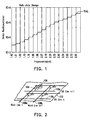
- Figure 1 is a graph illustrating a plot of the resistance versus the current for a multi-bit chalcogenide random access memory (RAM). As is illustrated by line 102, the resistance steps up according to each current increment.
- the resistance of chalcogenide may be tuned, however, one of the shortcomings associated with defining the stages through the resistance is that the resistance difference is difficult to sense because the sensing margin is small for multibit applications and the sensing time for the high resistance stage will be long. For example, assuming that there are 4 states of resistance and they are 5k, 50k, 500k and 5M Ohm, the current to read a cell is usually 20 ⁇ A.
- US Patent No. 4199692 discloses a method of reading a binary amorphous non-volatile RAM cell based on the two threshold voltages of two states "0" and "1".
- Calligaro et al. disclosed a dichotomic current-mode serial sensing methodology for multi-storage non-volatile memories in pages 302-304 of Circuits And Systems. 1995. Proceedings., Proceedings of the 38th Midwest Symposium on Rio De Janeiro, Brazil.
- Prior art document US-B-6 314 026 describes a reading method for multi-bit floating gate memory cells.
- the present invention provides a method for reading a memory cell structure that is capable of defining multiple bits per cell through the use of a threshold changing material.
- a method for reading a multibit memory cell according to claim 1 is provided.
- the multibit memory device is programmed prior to being read.
- the programming includes tuning a voltage threshold through the application of varying voltage pulses.
- the method of reading the multibit memory cell of the present invention may be applied in numerous memory/solid state device applications.
- One of the significant advantages of the read method is the speed and the sensing margin achieved when reading the current as opposed to sensing resistance.
- a threshold voltage associated with a threshold changing material is obtained by applying different energy pulses in order to define different threshold voltages.
- the threshold changing material is a chalcogenide material.
- V th the threshold voltage
- the current associated with each stage is distinguishable. Consequently, by sensing the current, the corresponding states may be determined. Therefore, within one memory core cell multiple states may exist and the different states correspond to a sensed current.
- FIG. 2 is a simplified schematic diagram of a portion of a typical chalcogenide memory array.
- Memory array portion 112 includes word lines 108 a and 108b, bit lines 110a and 110b, transistor device 104, and chalcogenide device 106.
- Transistor device 104 functions as a steering device, i.e., an access transistor, which provides access to chalcogenide device 106 from the corresponding word line and bit line.
- transistor device 104 may by an access P-N diode, a bipolar junction transistor (BIT), or other suitable transistor.
- chalcogenide device 106 functions as a memory cell.
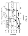
- Figure 3 is a normalized current (I)-normalized voltage (V) curve where different programming pulses were applied to a threshold changing material in order to define different threshold voltages.
- the V th of chalcogenide may be adjusted by applying energy into the film. Therefore, there may be different V th within a single memory core cell.
- the steering transistor of the selected cell may be activated and a certain energy pulse is applied to the cell.
- the energy pulse is associated with a certain duration and profile. For example, to program a cell a voltage from 0.1 V to 20 V may be applied. In one embodiment, the duration may be 1 nanosecond (ns) to 1000 ns.
- V th1 is associated with a first state
- V th2 is associated with a second state
- V th3 is associated with a third state
- V th4 is associated with a fourth state.
- Table 1 below provides a truth table associated with the four states illustrated in Figure 3 .
- state 1 is defined when the read voltage V a is between V th1 and V th2 .
- States 1 and 2 are defined when the read voltage V b is between V th2 and V th3 .
- States 1, 2 , and 3 are defined when the read voltage V c is between V th3 and V th4 .
- States 1, 2, 3, and 4 are defined when the read voltage V d is greater than V th4 .
- Figure 4 is a flow chart diagram illustrating the method operations for reading the multibit states associated with a threshold changing material.
- the method initiates with decision operation 122 where a current is measured at read voltage V b . If the current is high (on), then the method advances to operation 124 where the state is either state one or state two. The method then moves to decision operation 126 where the current is measured at read voltage V a . If the current is high (on), then the associated state is state one as indicated in box 128. If the current measured in decision operation 126 is low (off), then this is an indication of state two 130. Returning to decision operation 122, if the current measured at V b is low (Off), then this is an indication of either state three or four as represented by box 132.
- the method then proceeds to decision operation 134 where the current is measured at voltage V c . If the current measured at V c is high (on), then this is an indication of state three 136. If the current measured at V c is low (off), then the associated state here is state four as represented by box 138.
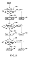
- Figure 5 is a flowchart diagram of an alternative method for reading the multibit states of a threshold changing material described with reference to Figure 4 .
- the method initiates with a decision operation 140 where a current is measured at voltage V a . If the current associated with read voltage V a indicates high (on), then the method proceeds to operation 142 which indicates that the state is either state two, three or four. The method then proceeds to decision operation 144 where the current is measured at read voltage V b If the current associated with V b is high (on), this indicates either state three or state four in box 146. The method then moves to decision operation 148 where the current is measured at voltage V c . If the voltage at V c is high (on), then state three is indicated as provided by box 150.
- a multibit chalcogenide memory is described herein.
- the multibit data are stored according to different threshold voltages.
- the threshold voltage is tuned by applying different energy pulses.
- two reading methods have been discussed. It should be appreciated in each of the reading methods the reading voltage should be higher than the threshold voltage. Accordingly, by changing the threshold voltage of the threshold changing material, a multibit memory is provided. As discussed above, a multibit non-volatile random access memory may be achieved in one embodiment of the invention.
- the multibit stages may be easily discerned. Reading the current suffices to provide a distinguishing feature. Furthermore, the reading speed is relatively fast as compared to other reading speeds, i.e., the speed associated with reading resistance.
Landscapes
- Engineering & Computer Science (AREA)
- Computer Hardware Design (AREA)
- Chemical & Material Sciences (AREA)
- Crystallography & Structural Chemistry (AREA)
- Semiconductor Memories (AREA)
- Read Only Memory (AREA)
Claims (8)
- Un procédé pour la lecture d'une cellule mémoire qui inclut un matériau changeant la résistance et qui agit comme un matériau (106) changeant le seuil, comprenant une étape d'application de tension sur le matériau (106) changeant le seuil, une étape de détermination du courant à l'état «circulation» ou «interruption» qui suit l'étape d'application de la tension et une étape de détermination de l'état de stockage sur la base d'un résultat de l'étape de détermination de l'état du courant,
l'étape d'application de courant comprend l'application d'une première tension de lecture sur le matériau changeant le seuil (106), où un niveau de la première tension lue se situe entre une paire de niveaux adjacents des tensions de seuil ;
l'étape de détermination du courant à l'état «circulation» ou «interruption» comprend la détermination d'un état «circulation» ou «interruption» d'un courant associé avec la première tension de lecture ;
caractérisé en ce que ladite cellule mémoire est une cellule mémoire multibit ayant plus de deux niveaux de tension de seuil et ;
l'étape de détermination de l'état de stockage comprend la distinction entre les multiples niveaux basés sur l'état «circulation» ou «interruption» du courant associé avec la première tension de lecture lue dans le but de déterminer les états possibles ou un état spécifique de la cellule mémoire multibit ; et
une deuxième tension de lecture, différente de la première tension lue, est appliquée sur le matériau (106) changeant le seuil si ce qui a été déterminé à travers les étapes de ci-dessus représente des états possibles de la cellule mémoire multibit. - Le procédé de la revendication 1, dans lequel la cellule mémoire multibit a été programmée avant d'être lue.
- Le procédé de la revendication 2, dans lequel la programmation de la cellule mémoire multibit comprend :l'application d'une tension située entre environ 0.1 volt et 20 volts sur le matériau (106) changeant le seuil.
- Le procédé de la revendication 3, dans lequel l'application de la tension située entre 0.1 volt et 20 volts comprend :l'application de la tension pour une durée située entre 1 nanoseconde et 1,000 nanosecondes.
- Le procédé de la revendication 1, dans lequel la cellule mémoire multibit est une cellule mémoire non-volatile.
- Le procédé de la revendication 2, dans lequel la programmation de la cellule mémoire multibit comprend :l'activation d'un transistor (104) de pilotage.
- Le procédé de la revendication 1, dans lequel un niveau de la deuxième tension lue se situe entre une autre paire de niveaux adjacents des tensions de seuil, comprenant en outre :la détermination d'un état «circulation» ou «interruption» d'un courant associé avec la deuxième tension lue ;etla détermination, parmi les états possibles de la revendication 1, d'un nouveau jeu d'états possibles ou l'état de la cellule mémoire multibit sur la base «circulation» ou «interruption» du courant associé avec la deuxième tension lue.
- Le procédé de la revendication 1, dans lequel le matériau (106) changeant le seuil est un matériau de chalcogénure.
Applications Claiming Priority (2)
| Application Number | Priority Date | Filing Date | Title |
|---|---|---|---|
| US10/465,012 US7180767B2 (en) | 2003-06-18 | 2003-06-18 | Multi-level memory device and methods for programming and reading the same |
| US465012 | 2003-06-18 |
Publications (2)
| Publication Number | Publication Date |
|---|---|
| EP1489623A1 EP1489623A1 (fr) | 2004-12-22 |
| EP1489623B1 true EP1489623B1 (fr) | 2008-10-15 |
Family
ID=33418170
Family Applications (1)
| Application Number | Title | Priority Date | Filing Date |
|---|---|---|---|
| EP03026610A Expired - Lifetime EP1489623B1 (fr) | 2003-06-18 | 2003-11-19 | Dispositif de mémoire multibit et méthodes de programmation et de lecture du même |
Country Status (6)
| Country | Link |
|---|---|
| US (1) | US7180767B2 (fr) |
| EP (1) | EP1489623B1 (fr) |
| JP (1) | JP5611499B2 (fr) |
| CN (1) | CN100578668C (fr) |
| DE (1) | DE60324117D1 (fr) |
| TW (1) | TWI223258B (fr) |
Families Citing this family (26)
| Publication number | Priority date | Publication date | Assignee | Title |
|---|---|---|---|---|
| US7308067B2 (en) | 2003-08-04 | 2007-12-11 | Intel Corporation | Read bias scheme for phase change memories |
| US7138687B2 (en) * | 2004-01-26 | 2006-11-21 | Macronix International Co., Ltd. | Thin film phase-change memory |
| ATE488842T1 (de) | 2004-09-30 | 2010-12-15 | Nxp Bv | Integrierte schaltung mit speicherzellen mit einem programmierbaren widerstand und verfahren zum adressieren von speicherzellen mit einem programmierbaren widerstand |
| US8116159B2 (en) | 2005-03-30 | 2012-02-14 | Ovonyx, Inc. | Using a bit specific reference level to read a resistive memory |
| KR100684908B1 (ko) * | 2006-01-09 | 2007-02-22 | 삼성전자주식회사 | 다수 저항 상태를 갖는 저항 메모리 요소, 저항 메모리 셀및 그 동작 방법 그리고 상기 저항 메모리 요소를 적용한데이터 처리 시스템 |
| US20070267620A1 (en) * | 2006-05-18 | 2007-11-22 | Thomas Happ | Memory cell including doped phase change material |
| US20080019257A1 (en) * | 2006-07-18 | 2008-01-24 | Jan Boris Philipp | Integrated circuit with resistivity changing material having a step-like programming characteristitic |
| US8084799B2 (en) * | 2006-07-18 | 2011-12-27 | Qimonda Ag | Integrated circuit with memory having a step-like programming characteristic |
| US7688618B2 (en) * | 2006-07-18 | 2010-03-30 | Qimonda North America Corp. | Integrated circuit having memory having a step-like programming characteristic |
| KR100887069B1 (ko) * | 2007-07-24 | 2009-03-04 | 주식회사 하이닉스반도체 | 상 변화 메모리 장치 |
| US7881100B2 (en) * | 2008-04-08 | 2011-02-01 | Micron Technology, Inc. | State machine sensing of memory cells |
| US20100090189A1 (en) * | 2008-09-15 | 2010-04-15 | Savransky Semyon D | Nanoscale electrical device |
| US7885101B2 (en) * | 2008-12-29 | 2011-02-08 | Numonyx B.V. | Method for low-stress multilevel reading of phase change memory cells and multilevel phase change memory |
| KR101057725B1 (ko) * | 2008-12-31 | 2011-08-18 | 주식회사 하이닉스반도체 | 멀티 레벨 셀 데이터 센싱 장치 및 그 방법 |
| US7929338B2 (en) | 2009-02-24 | 2011-04-19 | International Business Machines Corporation | Memory reading method for resistance drift mitigation |
| US8605495B2 (en) | 2011-05-09 | 2013-12-10 | Macronix International Co., Ltd. | Isolation device free memory |
| US9281061B2 (en) | 2012-09-19 | 2016-03-08 | Micron Technology, Inc. | Methods and apparatuses having a voltage generator with an adjustable voltage drop for representing a voltage drop of a memory cell and/or a current mirror circuit and replica circuit |
| KR102157357B1 (ko) * | 2014-06-16 | 2020-09-17 | 삼성전자 주식회사 | 메모리 장치 및 상기 메모리 장치의 독출 방법 |
| JP2016033843A (ja) * | 2014-07-31 | 2016-03-10 | 株式会社東芝 | 不揮発性記憶装置およびその駆動方法 |
| US10134470B2 (en) | 2015-11-04 | 2018-11-20 | Micron Technology, Inc. | Apparatuses and methods including memory and operation of same |
| US9978810B2 (en) | 2015-11-04 | 2018-05-22 | Micron Technology, Inc. | Three-dimensional memory apparatuses and methods of use |
| US10446226B2 (en) * | 2016-08-08 | 2019-10-15 | Micron Technology, Inc. | Apparatuses including multi-level memory cells and methods of operation of same |
| US10381075B2 (en) | 2017-12-14 | 2019-08-13 | Micron Technology, Inc. | Techniques to access a self-selecting memory device |
| US10546632B2 (en) * | 2017-12-14 | 2020-01-28 | Micron Technology, Inc. | Multi-level self-selecting memory device |
| US11302390B2 (en) * | 2020-07-10 | 2022-04-12 | Micron Technology, Inc. | Reading a multi-level memory cell |
| FR3148862B1 (fr) * | 2023-05-19 | 2025-10-17 | St Microelectronics Int Nv | Lecture d’un dispositif de mémoire non volatile multi-niveaux, en particulier à changement de phase, et dispositif de mémoire non volatile multi-niveaux |
Family Cites Families (18)
| Publication number | Priority date | Publication date | Assignee | Title |
|---|---|---|---|---|
| US3530441A (en) | 1969-01-15 | 1970-09-22 | Energy Conversion Devices Inc | Method and apparatus for storing and retrieving information |
| US4199692A (en) * | 1978-05-16 | 1980-04-22 | Harris Corporation | Amorphous non-volatile ram |
| JP3454821B2 (ja) * | 1991-08-19 | 2003-10-06 | エナージー・コンバーション・デバイセス・インコーポレーテッド | 電気的に消去可能な、直接重ね書き可能なマルチビット単セルメモリ素子およびそれらから作製したアレイ |
| US5508958A (en) * | 1994-09-29 | 1996-04-16 | Intel Corporation | Method and apparatus for sensing the state of floating gate memory cells by applying a variable gate voltage |
| US5714768A (en) * | 1995-10-24 | 1998-02-03 | Energy Conversion Devices, Inc. | Second-layer phase change memory array on top of a logic device |
| US5687112A (en) * | 1996-04-19 | 1997-11-11 | Energy Conversion Devices, Inc. | Multibit single cell memory element having tapered contact |
| JP3930074B2 (ja) * | 1996-09-30 | 2007-06-13 | 株式会社ルネサステクノロジ | 半導体集積回路及びデータ処理システム |
| US5812441A (en) * | 1996-10-21 | 1998-09-22 | Micron Technology, Inc. | MOS diode for use in a non-volatile memory cell |
| US5912839A (en) * | 1998-06-23 | 1999-06-15 | Energy Conversion Devices, Inc. | Universal memory element and method of programming same |
| US6141241A (en) * | 1998-06-23 | 2000-10-31 | Energy Conversion Devices, Inc. | Universal memory element with systems employing same and apparatus and method for reading, writing and programming same |
| AU763809B2 (en) * | 1999-02-11 | 2003-07-31 | Arizona Board Of Regents On Behalf Of The University Of Arizona, The | Programmable microelectronic devices and methods of forming and programming same |
| US6314014B1 (en) * | 1999-12-16 | 2001-11-06 | Ovonyx, Inc. | Programmable resistance memory arrays with reference cells |
| US6563156B2 (en) * | 2001-03-15 | 2003-05-13 | Micron Technology, Inc. | Memory elements and methods for making same |
| US6590807B2 (en) * | 2001-08-02 | 2003-07-08 | Intel Corporation | Method for reading a structural phase-change memory |
| JP2003100084A (ja) * | 2001-09-27 | 2003-04-04 | Toshiba Corp | 相変化型不揮発性記憶装置 |
| JP3749847B2 (ja) * | 2001-09-27 | 2006-03-01 | 株式会社東芝 | 相変化型不揮発性記憶装置及びその駆動回路 |
| DE60137788D1 (de) * | 2001-12-27 | 2009-04-09 | St Microelectronics Srl | Architektur einer nichtflüchtigen Phasenwechsel -Speichermatrix |
| EP1324345A1 (fr) * | 2001-12-27 | 2003-07-02 | STMicroelectronics S.r.l. | Mémoire non volatile à tension d'alimentation unique avec un décodeur de colonne du type cascode |
-
2003
- 2003-06-18 US US10/465,012 patent/US7180767B2/en not_active Expired - Lifetime
- 2003-11-13 TW TW092131759A patent/TWI223258B/zh not_active IP Right Cessation
- 2003-11-19 EP EP03026610A patent/EP1489623B1/fr not_active Expired - Lifetime
- 2003-11-19 DE DE60324117T patent/DE60324117D1/de not_active Expired - Lifetime
-
2004
- 2004-02-25 CN CN200410006005A patent/CN100578668C/zh not_active Expired - Lifetime
- 2004-05-07 JP JP2004138733A patent/JP5611499B2/ja not_active Expired - Lifetime
Also Published As
| Publication number | Publication date |
|---|---|
| TWI223258B (en) | 2004-11-01 |
| US20040257854A1 (en) | 2004-12-23 |
| JP2005012186A (ja) | 2005-01-13 |
| CN1574091A (zh) | 2005-02-02 |
| TW200501160A (en) | 2005-01-01 |
| CN100578668C (zh) | 2010-01-06 |
| DE60324117D1 (de) | 2008-11-27 |
| EP1489623A1 (fr) | 2004-12-22 |
| JP5611499B2 (ja) | 2014-10-22 |
| US7180767B2 (en) | 2007-02-20 |
Similar Documents
| Publication | Publication Date | Title |
|---|---|---|
| EP1489623B1 (fr) | Dispositif de mémoire multibit et méthodes de programmation et de lecture du même | |
| EP1489621B1 (fr) | Mémoire à accès aléatoire sans transistors | |
| US6462984B1 (en) | Biasing scheme of floating unselected wordlines and bitlines of a diode-based memory array | |
| EP1426966B1 (fr) | Cellule de mémoire non-volatile et dispositif de mémoire non-volatile à semiconducteurs | |
| US6590807B2 (en) | Method for reading a structural phase-change memory | |
| US6813177B2 (en) | Method and system to store information | |
| US8427862B2 (en) | Reading a phase change memory | |
| US5943260A (en) | Method for high-speed programming of a nonvolatile semiconductor memory device | |
| KR101214741B1 (ko) | 상 변화 메모리 | |
| US9318194B1 (en) | Apparatus and methods for sensing hard bit and soft bits | |
| JP2004519804A (ja) | 改善されたプログラミングを備えた不揮発性メモリ及び該プログラミングのための方法 | |
| US20040145944A1 (en) | Phase-change memory element and method of storing data therein | |
| US20060227591A1 (en) | Using higher current to read a triggered phase change memory | |
| US20060279979A1 (en) | Method of reading phase-change memory elements | |
| CN1767047A (zh) | 编制多阶相变记忆体装置的方法 | |
| WO2001063613A1 (fr) | Ecriture de donnees dans des cellules multiniveau | |
| US7894237B2 (en) | Programming multilevel cell phase change memories | |
| EP4244894B1 (fr) | Architecture et procédé de fonctionnement de mémoire nand | |
| WO2001063615A1 (fr) | Programmation de cellule selectionnable par utilisateur | |
| EP0851429A2 (fr) | Dispositif de détection de données et méthode pour cellule de mémoire multibit | |
| US7551503B2 (en) | Method for refreshing a flash memory | |
| EP1807841B1 (fr) | Memoire et procede de creation d'un mecanisme de rafraichissement base sur un seuil de moyennes | |
| CN100568390C (zh) | 含有包括可编程电阻器的存储单元的集成电路以及用于寻址包括可编程电阻器的存储单元的方法 | |
| EP1733398B1 (fr) | Circuit permettant d'acceder a une matrice memoire a chalcogenure | |
| JP2011150774A (ja) | 多次元のメモリ状態により特徴付けられる記憶された多ビットのデータ |
Legal Events
| Date | Code | Title | Description |
|---|---|---|---|
| PUAI | Public reference made under article 153(3) epc to a published international application that has entered the european phase |
Free format text: ORIGINAL CODE: 0009012 |
|
| 17P | Request for examination filed |
Effective date: 20031119 |
|
| AK | Designated contracting states |
Kind code of ref document: A1 Designated state(s): AT BE BG CH CY CZ DE DK EE ES FI FR GB GR HU IE IT LI LU MC NL PT RO SE SI SK TR |
|
| AX | Request for extension of the european patent |
Extension state: AL LT LV MK |
|
| 17Q | First examination report despatched |
Effective date: 20050309 |
|
| AKX | Designation fees paid |
Designated state(s): DE FR GB IT |
|
| 17Q | First examination report despatched |
Effective date: 20050309 |
|
| 17Q | First examination report despatched |
Effective date: 20050309 |
|
| GRAP | Despatch of communication of intention to grant a patent |
Free format text: ORIGINAL CODE: EPIDOSNIGR1 |
|
| GRAS | Grant fee paid |
Free format text: ORIGINAL CODE: EPIDOSNIGR3 |
|
| GRAA | (expected) grant |
Free format text: ORIGINAL CODE: 0009210 |
|
| AK | Designated contracting states |
Kind code of ref document: B1 Designated state(s): DE FR GB IT |
|
| REG | Reference to a national code |
Ref country code: GB Ref legal event code: FG4D |
|
| REF | Corresponds to: |
Ref document number: 60324117 Country of ref document: DE Date of ref document: 20081127 Kind code of ref document: P |
|
| PLBE | No opposition filed within time limit |
Free format text: ORIGINAL CODE: 0009261 |
|
| STAA | Information on the status of an ep patent application or granted ep patent |
Free format text: STATUS: NO OPPOSITION FILED WITHIN TIME LIMIT |
|
| 26N | No opposition filed |
Effective date: 20090716 |
|
| REG | Reference to a national code |
Ref country code: FR Ref legal event code: PLFP Year of fee payment: 13 |
|
| REG | Reference to a national code |
Ref country code: FR Ref legal event code: PLFP Year of fee payment: 14 |
|
| REG | Reference to a national code |
Ref country code: FR Ref legal event code: PLFP Year of fee payment: 15 |
|
| REG | Reference to a national code |
Ref country code: FR Ref legal event code: PLFP Year of fee payment: 16 |
|
| PGFP | Annual fee paid to national office [announced via postgrant information from national office to epo] |
Ref country code: IT Payment date: 20220831 Year of fee payment: 20 Ref country code: GB Payment date: 20220907 Year of fee payment: 20 |
|
| PGFP | Annual fee paid to national office [announced via postgrant information from national office to epo] |
Ref country code: FR Payment date: 20220907 Year of fee payment: 20 |
|
| PGFP | Annual fee paid to national office [announced via postgrant information from national office to epo] |
Ref country code: DE Payment date: 20220908 Year of fee payment: 20 |
|
| REG | Reference to a national code |
Ref country code: DE Ref legal event code: R071 Ref document number: 60324117 Country of ref document: DE |
|
| REG | Reference to a national code |
Ref country code: GB Ref legal event code: PE20 Expiry date: 20231118 |
|
| PG25 | Lapsed in a contracting state [announced via postgrant information from national office to epo] |
Ref country code: GB Free format text: LAPSE BECAUSE OF EXPIRATION OF PROTECTION Effective date: 20231118 |
|
| PG25 | Lapsed in a contracting state [announced via postgrant information from national office to epo] |
Ref country code: GB Free format text: LAPSE BECAUSE OF EXPIRATION OF PROTECTION Effective date: 20231118 |