EP1521103A1 - Reflektionsmindernder Film für die Frontscheibe eines Plasmadisplays und Herstellverfahren dafür - Google Patents
Reflektionsmindernder Film für die Frontscheibe eines Plasmadisplays und Herstellverfahren dafür Download PDFInfo
- Publication number
- EP1521103A1 EP1521103A1 EP04023590A EP04023590A EP1521103A1 EP 1521103 A1 EP1521103 A1 EP 1521103A1 EP 04023590 A EP04023590 A EP 04023590A EP 04023590 A EP04023590 A EP 04023590A EP 1521103 A1 EP1521103 A1 EP 1521103A1
- Authority
- EP
- European Patent Office
- Prior art keywords
- refractive index
- layer
- reflection film
- front panel
- plasma display
- Prior art date
- Legal status (The legal status is an assumption and is not a legal conclusion. Google has not performed a legal analysis and makes no representation as to the accuracy of the status listed.)
- Withdrawn
Links
- 238000000034 method Methods 0.000 title claims abstract description 21
- 239000010410 layer Substances 0.000 claims abstract description 146
- 239000000758 substrate Substances 0.000 claims abstract description 52
- 229920001940 conductive polymer Polymers 0.000 claims abstract description 34
- 239000011247 coating layer Substances 0.000 claims abstract description 29
- 238000012685 gas phase polymerization Methods 0.000 claims abstract description 15
- 239000000178 monomer Substances 0.000 claims abstract description 15
- 239000007800 oxidant agent Substances 0.000 claims description 18
- 229920000123 polythiophene Polymers 0.000 claims description 6
- YTPLMLYBLZKORZ-UHFFFAOYSA-N Thiophene Chemical compound C=1C=CSC=1 YTPLMLYBLZKORZ-UHFFFAOYSA-N 0.000 abstract description 8
- 229930192474 thiophene Natural products 0.000 abstract description 4
- 239000010408 film Substances 0.000 description 90
- OKKJLVBELUTLKV-UHFFFAOYSA-N Methanol Chemical compound OC OKKJLVBELUTLKV-UHFFFAOYSA-N 0.000 description 19
- 229920005989 resin Polymers 0.000 description 18
- 239000011347 resin Substances 0.000 description 18
- 239000011248 coating agent Substances 0.000 description 14
- 239000000203 mixture Substances 0.000 description 14
- 238000000576 coating method Methods 0.000 description 13
- 238000002834 transmittance Methods 0.000 description 10
- -1 for example Substances 0.000 description 9
- 230000000694 effects Effects 0.000 description 8
- 239000000463 material Substances 0.000 description 8
- 238000006116 polymerization reaction Methods 0.000 description 8
- 239000003054 catalyst Substances 0.000 description 6
- 239000000975 dye Substances 0.000 description 6
- 239000003960 organic solvent Substances 0.000 description 6
- 229920006267 polyester film Polymers 0.000 description 6
- 230000015572 biosynthetic process Effects 0.000 description 5
- 239000000049 pigment Substances 0.000 description 5
- ZNQVEEAIQZEUHB-UHFFFAOYSA-N 2-ethoxyethanol Chemical compound CCOCCO ZNQVEEAIQZEUHB-UHFFFAOYSA-N 0.000 description 4
- 239000011230 binding agent Substances 0.000 description 4
- BTANRVKWQNVYAZ-UHFFFAOYSA-N butan-2-ol Chemical compound CCC(C)O BTANRVKWQNVYAZ-UHFFFAOYSA-N 0.000 description 4
- 238000006748 scratching Methods 0.000 description 4
- 230000002393 scratching effect Effects 0.000 description 4
- ZWEHNKRNPOVVGH-UHFFFAOYSA-N 2-Butanone Chemical compound CCC(C)=O ZWEHNKRNPOVVGH-UHFFFAOYSA-N 0.000 description 3
- CSCPPACGZOOCGX-UHFFFAOYSA-N Acetone Chemical compound CC(C)=O CSCPPACGZOOCGX-UHFFFAOYSA-N 0.000 description 3
- 239000004925 Acrylic resin Substances 0.000 description 3
- LFQSCWFLJHTTHZ-UHFFFAOYSA-N Ethanol Chemical compound CCO LFQSCWFLJHTTHZ-UHFFFAOYSA-N 0.000 description 3
- XEKOWRVHYACXOJ-UHFFFAOYSA-N Ethyl acetate Chemical compound CCOC(C)=O XEKOWRVHYACXOJ-UHFFFAOYSA-N 0.000 description 3
- 229920001609 Poly(3,4-ethylenedioxythiophene) Polymers 0.000 description 3
- VYPSYNLAJGMNEJ-UHFFFAOYSA-N Silicium dioxide Chemical compound O=[Si]=O VYPSYNLAJGMNEJ-UHFFFAOYSA-N 0.000 description 3
- YXFVVABEGXRONW-UHFFFAOYSA-N Toluene Chemical compound CC1=CC=CC=C1 YXFVVABEGXRONW-UHFFFAOYSA-N 0.000 description 3
- 238000005229 chemical vapour deposition Methods 0.000 description 3
- 239000006185 dispersion Substances 0.000 description 3
- 238000004519 manufacturing process Methods 0.000 description 3
- 229910052751 metal Inorganic materials 0.000 description 3
- 239000002184 metal Substances 0.000 description 3
- 229910044991 metal oxide Inorganic materials 0.000 description 3
- 150000004706 metal oxides Chemical class 0.000 description 3
- 239000002245 particle Substances 0.000 description 3
- 239000002904 solvent Substances 0.000 description 3
- 238000004528 spin coating Methods 0.000 description 3
- GKWLILHTTGWKLQ-UHFFFAOYSA-N 2,3-dihydrothieno[3,4-b][1,4]dioxine Chemical compound O1CCOC2=CSC=C21 GKWLILHTTGWKLQ-UHFFFAOYSA-N 0.000 description 2
- 229920000178 Acrylic resin Polymers 0.000 description 2
- YLQBMQCUIZJEEH-UHFFFAOYSA-N Furan Chemical compound C=1C=COC=1 YLQBMQCUIZJEEH-UHFFFAOYSA-N 0.000 description 2
- 229910021578 Iron(III) chloride Inorganic materials 0.000 description 2
- 229920000877 Melamine resin Polymers 0.000 description 2
- 239000004640 Melamine resin Substances 0.000 description 2
- 229920000144 PEDOT:PSS Polymers 0.000 description 2
- KAESVJOAVNADME-UHFFFAOYSA-N Pyrrole Chemical compound C=1C=CNC=1 KAESVJOAVNADME-UHFFFAOYSA-N 0.000 description 2
- PPBRXRYQALVLMV-UHFFFAOYSA-N Styrene Chemical compound C=CC1=CC=CC=C1 PPBRXRYQALVLMV-UHFFFAOYSA-N 0.000 description 2
- 239000002253 acid Substances 0.000 description 2
- 239000012298 atmosphere Substances 0.000 description 2
- 230000005540 biological transmission Effects 0.000 description 2
- 238000006243 chemical reaction Methods 0.000 description 2
- 239000010949 copper Substances 0.000 description 2
- 239000003822 epoxy resin Substances 0.000 description 2
- 235000019441 ethanol Nutrition 0.000 description 2
- RBTARNINKXHZNM-UHFFFAOYSA-K iron trichloride Chemical compound Cl[Fe](Cl)Cl RBTARNINKXHZNM-UHFFFAOYSA-K 0.000 description 2
- PQXKHYXIUOZZFA-UHFFFAOYSA-M lithium fluoride Chemical compound [Li+].[F-] PQXKHYXIUOZZFA-UHFFFAOYSA-M 0.000 description 2
- 229910001507 metal halide Inorganic materials 0.000 description 2
- 150000005309 metal halides Chemical class 0.000 description 2
- 238000002156 mixing Methods 0.000 description 2
- RVTZCBVAJQQJTK-UHFFFAOYSA-N oxygen(2-);zirconium(4+) Chemical compound [O-2].[O-2].[Zr+4] RVTZCBVAJQQJTK-UHFFFAOYSA-N 0.000 description 2
- VLTRZXGMWDSKGL-UHFFFAOYSA-N perchloric acid Chemical compound OCl(=O)(=O)=O VLTRZXGMWDSKGL-UHFFFAOYSA-N 0.000 description 2
- 229920005668 polycarbonate resin Polymers 0.000 description 2
- 239000004431 polycarbonate resin Substances 0.000 description 2
- 229920000647 polyepoxide Polymers 0.000 description 2
- 229920001225 polyester resin Polymers 0.000 description 2
- 239000004645 polyester resin Substances 0.000 description 2
- 229920000642 polymer Polymers 0.000 description 2
- 230000000379 polymerizing effect Effects 0.000 description 2
- 239000000843 powder Substances 0.000 description 2
- PUZPDOWCWNUUKD-UHFFFAOYSA-M sodium fluoride Chemical compound [F-].[Na+] PUZPDOWCWNUUKD-UHFFFAOYSA-M 0.000 description 2
- 239000000126 substance Substances 0.000 description 2
- 238000003786 synthesis reaction Methods 0.000 description 2
- 229920001187 thermosetting polymer Polymers 0.000 description 2
- 239000010409 thin film Substances 0.000 description 2
- 229910052723 transition metal Inorganic materials 0.000 description 2
- 238000005406 washing Methods 0.000 description 2
- 229910001928 zirconium oxide Inorganic materials 0.000 description 2
- IRPGOXJVTQTAAN-UHFFFAOYSA-N 2,2,3,3,3-pentafluoropropanal Chemical compound FC(F)(F)C(F)(F)C=O IRPGOXJVTQTAAN-UHFFFAOYSA-N 0.000 description 1
- KLZUFWVZNOTSEM-UHFFFAOYSA-K Aluminum fluoride Inorganic materials F[Al](F)F KLZUFWVZNOTSEM-UHFFFAOYSA-K 0.000 description 1
- 229920000298 Cellophane Polymers 0.000 description 1
- 229920002284 Cellulose triacetate Polymers 0.000 description 1
- 229920001661 Chitosan Polymers 0.000 description 1
- RYGMFSIKBFXOCR-UHFFFAOYSA-N Copper Chemical compound [Cu] RYGMFSIKBFXOCR-UHFFFAOYSA-N 0.000 description 1
- XDTMQSROBMDMFD-UHFFFAOYSA-N Cyclohexane Chemical compound C1CCCCC1 XDTMQSROBMDMFD-UHFFFAOYSA-N 0.000 description 1
- YCKRFDGAMUMZLT-UHFFFAOYSA-N Fluorine atom Chemical compound [F] YCKRFDGAMUMZLT-UHFFFAOYSA-N 0.000 description 1
- 239000004695 Polyether sulfone Substances 0.000 description 1
- 239000004372 Polyvinyl alcohol Substances 0.000 description 1
- XUIMIQQOPSSXEZ-UHFFFAOYSA-N Silicon Chemical compound [Si] XUIMIQQOPSSXEZ-UHFFFAOYSA-N 0.000 description 1
- GWEVSGVZZGPLCZ-UHFFFAOYSA-N Titan oxide Chemical compound O=[Ti]=O GWEVSGVZZGPLCZ-UHFFFAOYSA-N 0.000 description 1
- BZHJMEDXRYGGRV-UHFFFAOYSA-N Vinyl chloride Chemical compound ClC=C BZHJMEDXRYGGRV-UHFFFAOYSA-N 0.000 description 1
- 239000005083 Zinc sulfide Substances 0.000 description 1
- NNLVGZFZQQXQNW-ADJNRHBOSA-N [(2r,3r,4s,5r,6s)-4,5-diacetyloxy-3-[(2s,3r,4s,5r,6r)-3,4,5-triacetyloxy-6-(acetyloxymethyl)oxan-2-yl]oxy-6-[(2r,3r,4s,5r,6s)-4,5,6-triacetyloxy-2-(acetyloxymethyl)oxan-3-yl]oxyoxan-2-yl]methyl acetate Chemical compound O([C@@H]1O[C@@H]([C@H]([C@H](OC(C)=O)[C@H]1OC(C)=O)O[C@H]1[C@@H]([C@@H](OC(C)=O)[C@H](OC(C)=O)[C@@H](COC(C)=O)O1)OC(C)=O)COC(=O)C)[C@@H]1[C@@H](COC(C)=O)O[C@@H](OC(C)=O)[C@H](OC(C)=O)[C@H]1OC(C)=O NNLVGZFZQQXQNW-ADJNRHBOSA-N 0.000 description 1
- NIXOWILDQLNWCW-UHFFFAOYSA-N acrylic acid group Chemical group C(C=C)(=O)O NIXOWILDQLNWCW-UHFFFAOYSA-N 0.000 description 1
- 239000000654 additive Substances 0.000 description 1
- 239000012790 adhesive layer Substances 0.000 description 1
- 239000005456 alcohol based solvent Substances 0.000 description 1
- 229920000180 alkyd Polymers 0.000 description 1
- 229910052782 aluminium Inorganic materials 0.000 description 1
- XAGFODPZIPBFFR-UHFFFAOYSA-N aluminium Chemical compound [Al] XAGFODPZIPBFFR-UHFFFAOYSA-N 0.000 description 1
- 229910001870 ammonium persulfate Inorganic materials 0.000 description 1
- 229910000410 antimony oxide Inorganic materials 0.000 description 1
- 239000003963 antioxidant agent Substances 0.000 description 1
- JKJWYKGYGWOAHT-UHFFFAOYSA-N bis(prop-2-enyl) carbonate Chemical compound C=CCOC(=O)OCC=C JKJWYKGYGWOAHT-UHFFFAOYSA-N 0.000 description 1
- WUKWITHWXAAZEY-UHFFFAOYSA-L calcium difluoride Chemical compound [F-].[F-].[Ca+2] WUKWITHWXAAZEY-UHFFFAOYSA-L 0.000 description 1
- 229910001634 calcium fluoride Inorganic materials 0.000 description 1
- 239000012461 cellulose resin Substances 0.000 description 1
- 229910000420 cerium oxide Inorganic materials 0.000 description 1
- 229910001914 chlorine tetroxide Inorganic materials 0.000 description 1
- 239000003086 colorant Substances 0.000 description 1
- 230000000052 comparative effect Effects 0.000 description 1
- 239000004020 conductor Substances 0.000 description 1
- 150000004696 coordination complex Chemical class 0.000 description 1
- 229920001577 copolymer Polymers 0.000 description 1
- 229910052802 copper Inorganic materials 0.000 description 1
- 238000003851 corona treatment Methods 0.000 description 1
- 150000001925 cycloalkenes Chemical class 0.000 description 1
- 238000000354 decomposition reaction Methods 0.000 description 1
- 238000000151 deposition Methods 0.000 description 1
- 230000008021 deposition Effects 0.000 description 1
- KPUWHANPEXNPJT-UHFFFAOYSA-N disiloxane Chemical class [SiH3]O[SiH3] KPUWHANPEXNPJT-UHFFFAOYSA-N 0.000 description 1
- 238000001035 drying Methods 0.000 description 1
- 239000000428 dust Substances 0.000 description 1
- 238000011156 evaluation Methods 0.000 description 1
- 239000010419 fine particle Substances 0.000 description 1
- 239000011737 fluorine Substances 0.000 description 1
- 229910052731 fluorine Inorganic materials 0.000 description 1
- 230000004313 glare Effects 0.000 description 1
- 150000004820 halides Chemical class 0.000 description 1
- 229920001519 homopolymer Polymers 0.000 description 1
- 229910003437 indium oxide Inorganic materials 0.000 description 1
- PJXISJQVUVHSOJ-UHFFFAOYSA-N indium(iii) oxide Chemical compound [O-2].[O-2].[O-2].[In+3].[In+3] PJXISJQVUVHSOJ-UHFFFAOYSA-N 0.000 description 1
- 229910052809 inorganic oxide Inorganic materials 0.000 description 1
- VPCCKEJZODGJBT-UHFFFAOYSA-K iron(3+) phenylmethanesulfonate Chemical compound [Fe+3].[O-]S(=O)(=O)Cc1ccccc1.[O-]S(=O)(=O)Cc1ccccc1.[O-]S(=O)(=O)Cc1ccccc1 VPCCKEJZODGJBT-UHFFFAOYSA-K 0.000 description 1
- LHOWRPZTCLUDOI-UHFFFAOYSA-K iron(3+);triperchlorate Chemical compound [Fe+3].[O-]Cl(=O)(=O)=O.[O-]Cl(=O)(=O)=O.[O-]Cl(=O)(=O)=O LHOWRPZTCLUDOI-UHFFFAOYSA-K 0.000 description 1
- 239000004973 liquid crystal related substance Substances 0.000 description 1
- ORUIBWPALBXDOA-UHFFFAOYSA-L magnesium fluoride Chemical compound [F-].[F-].[Mg+2] ORUIBWPALBXDOA-UHFFFAOYSA-L 0.000 description 1
- 229910001635 magnesium fluoride Inorganic materials 0.000 description 1
- 230000007257 malfunction Effects 0.000 description 1
- 229920000609 methyl cellulose Polymers 0.000 description 1
- 239000001923 methylcellulose Substances 0.000 description 1
- 235000010981 methylcellulose Nutrition 0.000 description 1
- 239000012046 mixed solvent Substances 0.000 description 1
- 150000003961 organosilicon compounds Chemical class 0.000 description 1
- TWNQGVIAIRXVLR-UHFFFAOYSA-N oxo(oxoalumanyloxy)alumane Chemical compound O=[Al]O[Al]=O TWNQGVIAIRXVLR-UHFFFAOYSA-N 0.000 description 1
- BMMGVYCKOGBVEV-UHFFFAOYSA-N oxo(oxoceriooxy)cerium Chemical compound [Ce]=O.O=[Ce]=O BMMGVYCKOGBVEV-UHFFFAOYSA-N 0.000 description 1
- VTRUBDSFZJNXHI-UHFFFAOYSA-N oxoantimony Chemical compound [Sb]=O VTRUBDSFZJNXHI-UHFFFAOYSA-N 0.000 description 1
- VLTRZXGMWDSKGL-UHFFFAOYSA-M perchlorate Chemical compound [O-]Cl(=O)(=O)=O VLTRZXGMWDSKGL-UHFFFAOYSA-M 0.000 description 1
- 230000002093 peripheral effect Effects 0.000 description 1
- 150000004965 peroxy acids Chemical class 0.000 description 1
- 239000001007 phthalocyanine dye Substances 0.000 description 1
- 229920006122 polyamide resin Polymers 0.000 description 1
- 229920006393 polyether sulfone Polymers 0.000 description 1
- 229920005672 polyolefin resin Polymers 0.000 description 1
- 239000004814 polyurethane Substances 0.000 description 1
- 229920002635 polyurethane Polymers 0.000 description 1
- 229920005749 polyurethane resin Polymers 0.000 description 1
- 229920002451 polyvinyl alcohol Polymers 0.000 description 1
- 239000004800 polyvinyl chloride Substances 0.000 description 1
- 229920000915 polyvinyl chloride Polymers 0.000 description 1
- 238000002360 preparation method Methods 0.000 description 1
- 230000001681 protective effect Effects 0.000 description 1
- 239000011241 protective layer Substances 0.000 description 1
- 230000035484 reaction time Effects 0.000 description 1
- 150000003839 salts Chemical class 0.000 description 1
- MABNMNVCOAICNO-UHFFFAOYSA-N selenophene Chemical compound C=1C=C[se]C=1 MABNMNVCOAICNO-UHFFFAOYSA-N 0.000 description 1
- 229910052710 silicon Inorganic materials 0.000 description 1
- 239000010703 silicon Substances 0.000 description 1
- 239000000377 silicon dioxide Substances 0.000 description 1
- 229910052814 silicon oxide Inorganic materials 0.000 description 1
- 229910052709 silver Inorganic materials 0.000 description 1
- 239000004332 silver Substances 0.000 description 1
- 235000013024 sodium fluoride Nutrition 0.000 description 1
- 239000011775 sodium fluoride Substances 0.000 description 1
- 230000003595 spectral effect Effects 0.000 description 1
- 238000004544 sputter deposition Methods 0.000 description 1
- 238000004381 surface treatment Methods 0.000 description 1
- 230000002195 synergetic effect Effects 0.000 description 1
- 150000003577 thiophenes Chemical class 0.000 description 1
- MZQZQKZKTGRQCG-UHFFFAOYSA-J thorium tetrafluoride Chemical compound F[Th](F)(F)F MZQZQKZKTGRQCG-UHFFFAOYSA-J 0.000 description 1
- OGIDPMRJRNCKJF-UHFFFAOYSA-N titanium oxide Inorganic materials [Ti]=O OGIDPMRJRNCKJF-UHFFFAOYSA-N 0.000 description 1
- 150000003624 transition metals Chemical class 0.000 description 1
- 238000011282 treatment Methods 0.000 description 1
- 229940124543 ultraviolet light absorber Drugs 0.000 description 1
- 238000007740 vapor deposition Methods 0.000 description 1
- 125000000391 vinyl group Chemical group [H]C([*])=C([H])[H] 0.000 description 1
- 229920002554 vinyl polymer Polymers 0.000 description 1
- XLYOFNOQVPJJNP-UHFFFAOYSA-N water Substances O XLYOFNOQVPJJNP-UHFFFAOYSA-N 0.000 description 1
- 229910052984 zinc sulfide Inorganic materials 0.000 description 1
- DRDVZXDWVBGGMH-UHFFFAOYSA-N zinc;sulfide Chemical compound [S-2].[Zn+2] DRDVZXDWVBGGMH-UHFFFAOYSA-N 0.000 description 1
Images
Classifications
-
- H—ELECTRICITY
- H01—ELECTRIC ELEMENTS
- H01J—ELECTRIC DISCHARGE TUBES OR DISCHARGE LAMPS
- H01J11/00—Gas-filled discharge tubes with alternating current induction of the discharge, e.g. alternating current plasma display panels [AC-PDP]; Gas-filled discharge tubes without any main electrode inside the vessel; Gas-filled discharge tubes with at least one main electrode outside the vessel
- H01J11/20—Constructional details
- H01J11/34—Vessels, containers or parts thereof, e.g. substrates
- H01J11/44—Optical arrangements or shielding arrangements, e.g. filters, black matrices, light reflecting means or electromagnetic shielding means
-
- G—PHYSICS
- G02—OPTICS
- G02B—OPTICAL ELEMENTS, SYSTEMS OR APPARATUS
- G02B1/00—Optical elements characterised by the material of which they are made; Optical coatings for optical elements
- G02B1/10—Optical coatings produced by application to, or surface treatment of, optical elements
- G02B1/11—Anti-reflection coatings
- G02B1/111—Anti-reflection coatings using layers comprising organic materials
-
- Y—GENERAL TAGGING OF NEW TECHNOLOGICAL DEVELOPMENTS; GENERAL TAGGING OF CROSS-SECTIONAL TECHNOLOGIES SPANNING OVER SEVERAL SECTIONS OF THE IPC; TECHNICAL SUBJECTS COVERED BY FORMER USPC CROSS-REFERENCE ART COLLECTIONS [XRACs] AND DIGESTS
- Y10—TECHNICAL SUBJECTS COVERED BY FORMER USPC
- Y10T—TECHNICAL SUBJECTS COVERED BY FORMER US CLASSIFICATION
- Y10T428/00—Stock material or miscellaneous articles
- Y10T428/26—Web or sheet containing structurally defined element or component, the element or component having a specified physical dimension
- Y10T428/263—Coating layer not in excess of 5 mils thick or equivalent
- Y10T428/264—Up to 3 mils
- Y10T428/265—1 mil or less
Definitions
- the present invention relates to an anti-reflection film for plasma display front panel, and more particularly to an anti-reflection film which has excellent anti-reflection properties and is excellent in transparency, near infrared ray shielding properties, color tone correction properties and antistatic properties, and a process for producing the anti-reflection film.
- plasma displays of rear projection screen systems having large screens have been put into practical use.
- front panels are frequently fitted for the purpose of protecting the screens, and in order to prevent scratching on the surfaces, protective films having a hard coating layer are often employed.
- the plasma displays have screens of larger size and flatter surface than the conventional cathode ray tube televisions, reflected peripheral environment or people in the screen attributable to much light reflection are observed. Furthermore, if there is reflected external environment in the screen attributable to the light reflection, visibility of an image is markedly lowered because of low luminance. Then, in order to enhance contrast of an image, a film containing a dye or a pigment is sometimes stuck to a transparent resin substrate for constituting the front panel. In this case, however, there is a limit in the amount of the dye or the pigment added because the visible light transmittance is lowered.
- Japanese Patent Laid-Open Publication No. 359024/2001 discloses a front panel having, as a film of this type, an anti-reflection film of a laminated structure consisting of a high-refractive index layer obtained by curing a composition containing particles of a metal oxide such as zirconium oxide or antimony oxide and a low-refractive index layer composed of a cured product of an organosilicon compound.
- this anti-reflection film however, there is a problem of a bad balance between transparency and antistatic properties.
- plasma displays release near infrared rays and electromagnetic waves out of the devices in principle. Since the near infrared rays become causes of malfunctions of codeless telephones, remote controllers of infrared ray system, etc., they need to be shielded. Also the electromagnetic waves sometimes exert bad influences on the equipment, and recently, for the reason that there is a possibility of doing harm to the human bodies, regulation by law is being made.
- a method of using a metal mesh such as a copper mesh or an alternating multi-layer film composed of a metal thin film and a metal oxide such as indium oxide is known.
- a method of dispersing a dye that absorbs near infrared rays in a transparent resin is known. In this method, however, there is a problem of lowering of visible light transmittance.
- a film having a specific conductive polymer layer has a good balance between the visible light transmittance and the near infrared ray shielding effect, and the color tone can be controlled by the thickness of the conductive polymer layer, and this film has excellent properties as an anti-reflection film for plasma display front panel. Further, the conductive polymer layer has excellent antistatic properties and exhibits excellent handling properties in the production of a plasma display front panel.
- the following anti-reflection film for plasma display front panel and the following process for producing the anti-reflection film are provided.
- substrates made of, for example, polyester resin, triacetyl cellulose resin, polycarbonate resin, allyl carbonate resin, polyether sulfone resin, polyacrylate resin, cycloolefin resin and acrylic styrene resin.
- the substrate may have been subjected to various surface treatments, such as corona discharge treatment.
- the form of the substrate is not restricted at all, but taking mass production capability into consideration, a substrate in the form of a roll is preferable.
- the substrate may contain various additives, for example, colorants such as dyes and pigments, ultraviolet light absorbers and antioxidants.
- the material to constitute the hard coating layer is not specifically restricted either, and examples of the materials include siloxane resin, acrylic resin, melamine resin and epoxy resin. These resins can be used singly or in combination of two or more kinds. A dispersion wherein fine particles of an inorganic oxide such as silica are dispersed in the above resin is also preferably employed.
- a hard coating layer having been subjected to antiglare treatment can be also employed without any problem.
- the thickness of the hard coating layer is preferably in the range of 0.1 to 50 ⁇ m. If the thickness of the hard coating layer is less than 0.1 ⁇ m, it sometimes becomes difficult to firmly fix the high-refractive index layer. On the other hand, a hard coating layer having a thickness of more than 50 ⁇ m is sometimes difficult to produce, or when such a hard coating layer is used for films, flexing properties are sometimes lowered.
- the thickness of the hard coating layer is desired to be in the range of 0.1 to 50 ⁇ m, preferably 0.5 to 30 ⁇ m, more preferably 1 to 20 ⁇ m.
- the low-refractive index layer has a refractive index (Na-D ray refractive index, measuring temperature: 25°C) of 1.35 to 1.50.
- the refractive index of the low-refractive index layer is less than 1.35, the kinds of the materials employable are excessively restricted. On the other hand, if the refractive index exceeds 1.5, anti-reflection effect is sometimes lowered when the low-refractive index layer is combined with a high-refractive index layer.
- the refractive index of the low-refractive index layer is desired to be in the range of 1.35 to 1.50, preferably 1.35 to 1.45, more preferably 1.35 to 1.42.
- the difference in the refractive index between the low-refractive index layer and the high-refractive index layer is desired to be not less than 0.05, preferably 0.1 to 0.5, more preferably 0.15 to 0.5.
- the thickness of the low-refractive index layer is not specifically restricted, but for example, it is preferably in the range of 0.05 to 1 ⁇ m.
- the thickness of the low-refractive index layer is less than 0.05 ⁇ m, adhesion strength of the low-refractive index layer to the high-refractive index layer as a base is sometimes lowered, or resistance to scratching is sometimes lowered.
- a low-refractive index layer having a thickness of more than 1 ⁇ m is difficult to uniformly form, and besides, light transmittance and resistance to scratching are sometimes lowered.
- the thickness of the low-refractive index layer is desired to be in the range of 0.05 to 1 ⁇ m, preferably 0.05 to 0.5 ⁇ m, more preferably 0.05 to 0.3 ⁇ m.
- the thickness of the low-refractive index layer is defined as an average of practically measured values (10 points) from a transmission electron microscope photograph of a section of a slice of the layer. In case of a layer (coating film) having an uneven lower surface, the thickness is defined as a distance between average lines of roughness curves (measured length: 1 ⁇ m) defined by JIS B0601.
- the low-refractive index layer can be formed by the use of, for example, a curing composition for forming a low-refractive index layer.
- the curing composition for forming a low-refractive index layer is, for example, a composition obtained by dispersing, in a thermosetting or ultraviolet curing resin binder, one or more kinds of low-refractive index material fine powders (average particle diameter: 0.3 - 200 nm, preferably 0.5 - 100 nm) selected from magnesium fluoride (refractive index: 1.38), silicon oxide (refractive index: 1.46), aluminum fluoride (refractive index: 1.33 - 1.39), calcium fluoride (refractive index: 1.44), lithium fluoride (refractive index: 1.36 - 1.37), sodium fluoride (refractive index: 1.32 - 1.34) and thorium fluoride (refractive index: 1.45 -1.5) .
- the resin binder is appropriately selected from polyester resin, acrylic resin, vinyl resin, polycarbonate resin, polyolefin resin, polyurethane resin, melamine resin, epoxy resin, polyamide resin, alkyd resin, vinyl chloride resin, fluororesin, silicon resin and the like.
- composition containing a fluorine type polymer is also preferably employed.
- the high-refractive index layer has a refractive index (Na-D ray refractive index, measuring temperature: 25°C) of 1.45 to 2.1.
- the refractive index of the high-refractive index layer is less than 1.45, anti-reflection effect is sometimes markedly lowered when the high-refractive index layer is combined with the low-refractive index layer.
- the refractive index exceeds 2.1, the kinds of the materials employable are excessively restricted.
- the refractive index of the high-refractive index layer is desired to be in the range of 1.45 to 2.1, preferably 1.55 to 2.0, more preferably 1.6 to 1.9.
- the thickness of the high-refractive index layer is not specifically restricted, but for example, it is preferably in the range of 0.05 to 30 ⁇ m.
- the thickness of the high-refractive index layer is less than 0.05 ⁇ m, anti-reflection effect and adhesion strength to the substrate are sometimes lowered when the high-refractive index layer is combined with the low-refractive index layer.
- a high-refractive index layer having a thickness of more than 30 ⁇ m it sometimes becomes difficult to uniformly form a non-continuous high-refractive index layer.
- the thickness of the high-refractive index layer is desired to be in the range of 0.05 to 30 ⁇ m, preferably 0.05 to 5 ⁇ m, more preferably 0.06 to 0.5 ⁇ m.
- the thickness of the low-refractive index layer is defined as an average of practically measured values (10 points) from a transmission electron microscope photograph of a section of a slice of the layer. In case of a layer (coating film) having an uneven lower surface, the thickness is defined as a distance between average lines of roughness curves (measured length: 1 ⁇ m) defined by JIS B0601.
- the thickness of the high-refractive index layer means a vertical distance between the lower surface and the upper surface (sectional height).
- the high-refractive index layer can be formed by the use of, for example, a curing composition for forming a high-refractive index layer.
- the curing composition for forming a high-refractive index layer is, for example, a thermosetting or ultraviolet curing composition obtained by dispersing, in a binder resin, a high-refractive index material fine powder (average particle diameter: 0.3 - 200 nm, preferably 0.5 - 100 nm) selected from cerium oxide (refractive index: 2.2 - 2.5), zinc sulfide (refractive index: 2.2 - 2.3), titanium oxide (refractive index: 2.2 - 2.7), zirconium oxide (refractive index: 1.95 - 2.0) and aluminum oxide (refractive index: 1.59 - 1.62) .
- binder resins examples include the same resins as previously described for the composition for forming the low-refractive index layer.
- polythiophene or its derivative is preferable from the viewpoints of transparency and color tone. More specifically, a homopolymer or a copolymer obtained by polymerizing thiophene or a thiophene derivative is preferable, and such polymers are publicly known (see, for example, Japanese Patent Laid-Open Publication No. 90060/1995). Of these, polythiophene or poly(3,4-ethylenedioxythiophene) is particularly preferably employed.
- the conductive layer comprising such a conductive polymer can be formed by coating a substrate or a laminate with a coating dispersion of the conductive polymer.
- the conductive layer is formed by gas phase polymerization as described below, the resulting conductive layer exhibits excellent adhesion to the substrate.
- the conductive layer formed by the gas phase polymerization is obtainable as a thin film and is excellent in the adhesion to the substrate, transparency and controllability of the film thickness. Therefore, the gas phase polymerization is particularly preferably employed.
- gas phase polymerization used herein means a process comprising applying an oxidizing agent to a surface of a substrate in a thickness of the order of several ⁇ m and bringing a monomer in a gas state into contact with the oxidizing agent to promote polymerization and thereby form a conductive polymer film on the substrate.
- Such a conductive layer can be prepared by a process described in Japanese Patent Laid-Open Publication No. 82105/2003.
- the type of the oxidizing agent for use in the invention should not be restricted, but halides of transition metals, transition metal salts having strong acid residual group such as perchloric acid, per acids such as peroxo acid and their salts, etc. are employed. Of these, CuCl 3 , FeCl 3 , iron(III) toluenesulfonate, iron(III) perchlorate, Cu (ClO 4 ) 2 6H 2 O, (NH 4 ) 2 S 2 O 8 are particularly preferable.
- the oxidizing agent is dissolved in an organic solvent prior to use.
- the organic solvent for use in the invention is selected from methyl alcohol, 2-butyl alcohol, ethyl cellosolve, ethyl alcohol, cyclohexane, acetone, ethyl acetate, toluene and methyl ethyl ketone.
- These organic solvents can be used singly or in combination of two to four kinds.
- an organic solvent obtained by mixing methyl alcohol, 2-butyl alcohol and ethyl cellosolve in a mixing ratio of 7:2:1, 6:2:2, 6:3:1 or 5:3:2 is employed.
- a high-molecular weight substance such as polyurethane, polyvinyl chloride, polyvinyl alcohol, methyl cellulose or chitosan, in combination with the organic solvent to enhance the adhesion strength.
- the monomer is subjected to gas phase polymerization, and in the gas phase polymerization, the reaction temperature is preferably in the range of 0 to 100°C.
- the surface of the substrate is coated with the oxidizing agent of 0.5 to 10% by weight in a thickness of the order of several ⁇ m.
- the solvent conditions vary depending upon the type of the substrate used, and usually, a mixture of two or more kinds of organic solvents is employed.
- the substrate having been coated with the oxidizing agent is dried by a hot air dryer at a temperature of not higher than 80°C, taking decomposition of the oxidizing agent into consideration.
- a monomer selected from the group consisting of pyrrole, thiophene, furan, selenophene, 3,4-ethylenedioxythiophene and their derivatives is vaporized and brought into contact with the substrate having been coated with the oxidizing agent to perform polymerization reaction on the surface of the substrate.
- methods to vaporize the monomer include a method of distilling the monomer at a temperature of 0 to 100°C in a closed chamber and a CVD (chemical vapor deposition) method.
- CVD chemical vapor deposition
- washing is carried out to remove the unreacted monomer and the oxidizing agent.
- an alcohol such as methanol is usually used, and in some cases, water may be used.
- a series of the above steps can be carried out batchwise or continuously, and the operations from the polymerization of the monomer to the formation of the conductive layer can be carried out as a series of the operations.
- the resulting conductive polymer film has a pencil hardness of about 1H to 3H, has excellent adhesion to the substrate and exhibits satisfactory resistance to alcohol solvents.
- the thickness of the conductive layer is preferably in the range of 1 to 2000 nm. If the thickness is less than 1 nm, pinholes or the like are liable to occur, and hence, film formation becomes difficult. Further, the surface resistance is increased and the antistatic properties are deteriorated. If the thickness exceeds 2000 nm, transparency and color tone are markedly deteriorated though the surface resistance is good, and such a layer cannot be used for an anti-reflection film.
- a particularly preferable thickness is in the range of 5 to 300 nm from the viewpoint of a balance between transparency, color tone and surface resistance.
- the surface resistance of the conductive layer is in the range of 10 2 ⁇ / ⁇ to 10 8 ⁇ / ⁇ .
- the anti-reflection film may have a laminated structure of substrate/hard coating layer/conductive layer, substrate/conductive layer/hard coating layer, or the like.
- the hard coating layer, the conductive layer, the high-refractive index layer and the low-refractive index layer may be provided on the upper surface of the substrate or the lower surface thereof, or may be provided on both surfaces.
- An anti-reflection film having a hard coating layer and a conductive layer comprising a conductive polymer formed by gas phase polymerization on the upper or the lower surface or both surfaces of the substrate is useful as an antistatic film.
- An anti-reflection film having at least a hard coating layer, a high-refractive index layer having a refractive index of 1.45 to 2.1 and a low-refractive index layer having a refractive index of 1.35 to 1.5 which are laminated in this order on at least one surface of the substrate and having a conductive layer comprising a conductive polymer between the hard coating layer and the high-refractive index layer or between the substrate and the hard coating layer is excellent in the antistatic properties and the anti-reflection properties.
- the anti-reflection film of the invention it is possible to appropriately provide a medium-refractive index layer, a protective layer, an adhesive layer or the like on at least one surface of each layer, when needed.
- functions other than the anti-reflection function and the antistatic function are not restricted at all, and a near infrared ray shielding layer, an electromagnetic wave shielding layer, a color tone correction layer and the like can be provided when needed.
- a near infrared ray shielding layer or the color tone correction layer a transparent resin film containing a dye or a pigment, such as a phthalocyanine dye or a metal complex, or a substrate in which such dye or pigment is dispersed is known.
- the electromagnetic wave shielding layer a lattice-like conductor such as a metal mesh, a multi-layer film consisting of silver and a metal oxide, an ITO film or the like is known.
- the anti-reflection film for plasma display front panel according to the invention has a surface resistance of 10 6 ⁇ / ⁇ to 10 12 ⁇ / ⁇ and a total light transmittance of not less than 80%.
- the hard coating layer, the conductive layer comprising a conductive polymer, the high-refractive index layer and the low-refractive index layer have only to be formed in an arbitrary order on a surface of the substrate, and formation of each layer is as described above.
- the conductive layer comprising a conductive polymer is preferably formed by applying an oxidizing agent onto a surface of a substrate or a laminate (e.g., laminate of substrate and hard coating layer) where the conductive layer is to be formed and bringing a monomer in a gas state into contact with the oxidizing agent to perform gas phase polymerization, as described above.
- the anti-reflection film for plasma display front panel according to the present invention has excellent anti-reflection properties and is excellent in transparency, near infrared ray shielding properties, color tone correction properties and antistatic properties.
- a polyester film A4300 (available from Toyobo Co., Ltd., film thickness: 100 ⁇ m) was coated with "Desolite Z7501" (available from JSR Co., Ltd.) as a hard coating agent, and the coating agent was dried in an oven under the conditions of 80°C and 1 minute to form a coating film. Then, the coating film was subjected to ultraviolet curing in the atmosphere by the use of a metal halide lamp under the conditions of 0.3 J/cm 2 to form a hard coating layer having a thickness of 3 ⁇ m.
- the polyester film having the hard coating layer was coated with the catalyst solution prepared in Synthesis Example by spin coating, followed by drying at a temperature of 60°C for 3 minutes.
- the color of the polyester film coated with the catalyst solution or the polyester film having the hard coating layer was light yellow.
- the polyester film having the hard coating layer and the catalyst coating film was placed in a CVD chamber designed so as to form a saturated 3,4-ethylenedioxythiophene monomer, and the substrate having been coated with the catalyst solution was subjected to reaction for 30 seconds. Thereafter, the polyester film was washed with a methanol solvent to remove the unreacted substance, whereby a conductive layer was formed.
- the conductive layer was coated with "Desolite KZ7987B" (available from JSR Co., Ltd.) as a curing composition for forming a high-refractive index layer by the use of a wire bar coater, and the composition was dried in an oven under the conditions of 80°C and 1 minute to form a coating film. Then, the coating film was subjected to ultraviolet curing in the atmosphere by the use of a metal halide lamp under the conditions of 0.3 J/cm 2 to form a high-refractive index layer having a thickness of 0.1 ⁇ m.
- "Desolite KZ7987B” available from JSR Co., Ltd.
- the high-refractive index layer was coated with "Opstar JN7215" (available from JSR Co., Ltd.) as a curing composition for forming a low-refractive index layer by the use of a wire bar coater, and the composition was air dried at room temperature for 5 minutes to form a coating film. Then, the coating film was heated in an oven under the conditions of 140°C and 1 minute to form a low-refractive index layer having a thickness of 0.1 ⁇ m.
- "Opstar JN7215” available from JSR Co., Ltd.
- Adhesion properties of the conductive layer formed on the substrate were evaluated in accordance with the cross-cut cellophane tape peel test of JIS K5400, that is, the adhesion properties were evaluated by a residual film ratio (%) to the total 100 squares (each square: 1 mm 2 ). The result is set forth in Table 1.
- the resulting anti-reflection film was measured on the reflectance, total light transmittance, turbidity (haze value), yellowness (b*) and surface resistance by the following measuring methods.
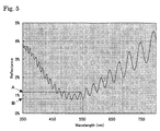
- the reflectance (minimum reflectance at the measuring wavelength) and the total light transmittance of the resulting anti-reflection film were measured by a spectral reflectance measuring device (autographic recording spectrophotometer U-3410 incorporated with large sample room integrating sphere attachment 150-09090, manufactured by Hitachi, Ltd.) in accordance with JIS K7105 (measuring method A). That is to say, the reflectance and the total light transmittance at the central point of interference vibration in the vicinity of 550 nm were measured and evaluated using a reflectance of an aluminum deposition film as a reference (100%). The results are set forth in Table 1.
- the haze value and the yellowness (b*) of the resulting anti-reflection film were measured in accordance with ASTM D1003 using a color haze meter (manufactured by Suga Seisakusho K.K.). The results are set forth in Table 1.
- the surface resistance of the resulting anti-reflection film was measured using a high resistance meter (HP4339 manufactured by Hewlett Packard Co.) and "Loresta EP” (manufactured by Mitsubishi Chemical Co.). The result is set forth in Table 1.
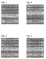
- An anti-reflection film having a film structure of Fig. 2 was prepared, and the reflectance, surface resistance, etc. of the anti-reflection film were evaluated. The results are set forth in Table 1.
- poly(3,4-ethylenedioxythiophene) was used for the conductive layer.
- An anti-reflection film having a film structure of Fig. 3 was prepared using, as a conductive layer, a layer formed by spin coating with aqueous dispersion of poly(3,4-ethylenedioxythiophene) "Baytron P" (available from Bayer), and the reflectance, surface resistance, etc. of the anti-reflection film were evaluated. The results are set forth in Table 1.
- An anti-reflection film having a film structure of Fig. 4 was prepared, and the reflectance, surface resistance, etc. of the anti-reflection film were evaluated.
- the results are set forth in Table 1.
- As the conductive layer a layer formed by spin coating with "Baytron P" was used, similarly to Example 3.
- an anti-reflection film for plasma display front panel having a hard coating layer, a conductive layer comprising a conductive polymer, a high-refractive index layer and a low-refractive index layer, which are provided in an arbitrary order on at least one surface of a substrate. Also disclosed is a process for producing the anti-reflection film, comprising forming a conductive layer comprising a conductive polymer on a surface of a substrate by gas phase polymerization of a monomer such as thiophene.
- the anti-reflection film for plasma display front panel of the invention has excellent anti-reflection properties and is excellent in transparency, near infrared ray shielding properties, color tone correction properties and antistatic properties.
- the process of the invention can produce an anti-reflection film for plasma display front panel having excellent adhesion between the substrate and the conductive layer.
Landscapes
- Physics & Mathematics (AREA)
- General Physics & Mathematics (AREA)
- Optics & Photonics (AREA)
- Electromagnetism (AREA)
- Engineering & Computer Science (AREA)
- Plasma & Fusion (AREA)
- Surface Treatment Of Optical Elements (AREA)
- Laminated Bodies (AREA)
- Devices For Indicating Variable Information By Combining Individual Elements (AREA)
Applications Claiming Priority (2)
| Application Number | Priority Date | Filing Date | Title |
|---|---|---|---|
| JP2003346086 | 2003-10-03 | ||
| JP2003346086A JP2005114852A (ja) | 2003-10-03 | 2003-10-03 | プラズマディスプレイ前面板用反射防止フィルム及びその製造方法 |
Publications (1)
| Publication Number | Publication Date |
|---|---|
| EP1521103A1 true EP1521103A1 (de) | 2005-04-06 |
Family
ID=34309169
Family Applications (1)
| Application Number | Title | Priority Date | Filing Date |
|---|---|---|---|
| EP04023590A Withdrawn EP1521103A1 (de) | 2003-10-03 | 2004-10-01 | Reflektionsmindernder Film für die Frontscheibe eines Plasmadisplays und Herstellverfahren dafür |
Country Status (5)
| Country | Link |
|---|---|
| US (1) | US20050074603A1 (de) |
| EP (1) | EP1521103A1 (de) |
| JP (1) | JP2005114852A (de) |
| KR (1) | KR20050033439A (de) |
| TW (1) | TW200523569A (de) |
Cited By (2)
| Publication number | Priority date | Publication date | Assignee | Title |
|---|---|---|---|---|
| FR2904431A1 (fr) * | 2006-07-31 | 2008-02-01 | Essilor Int | Article d'optique a proprietes antistatiques et anti-abrasion, et procede de fabrication |
| CN106772712A (zh) * | 2015-11-24 | 2017-05-31 | 中国航空工业集团公司北京航空材料研究院 | 一种低发射的保护性防眩电磁屏蔽复合窗膜 |
Families Citing this family (18)
| Publication number | Priority date | Publication date | Assignee | Title |
|---|---|---|---|---|
| DE102004012319A1 (de) * | 2004-03-11 | 2005-09-22 | H.C. Starck Gmbh | Funktionsschichten für optische Anwendungen auf Basis von Polythiophenen |
| JP2007065036A (ja) * | 2005-08-29 | 2007-03-15 | Kao Corp | 光学器材用液剤 |
| KR100699624B1 (ko) | 2005-11-16 | 2007-03-23 | 주식회사 에이스 디지텍 | 대전방지 고해상 방현 필름의 제조방법 및 이를 이용한 대전방지 고해상 방현 필름 |
| KR100719590B1 (ko) * | 2005-12-28 | 2007-05-17 | 삼성에스디아이 주식회사 | 플라즈마 디스플레이 패널 |
| KR101255234B1 (ko) * | 2006-02-20 | 2013-04-16 | 삼성디스플레이 주식회사 | 전도성 박막 및 이를 포함하는 유기 전계 발광 소자 |
| JP5154773B2 (ja) * | 2006-07-19 | 2013-02-27 | リンテック株式会社 | 反射防止フィルム |
| DE102006048473A1 (de) * | 2006-10-11 | 2008-04-17 | Sefar Ag | Rückprojektionsgewebe, Rückprojektionsbildwand und Rückprojektionssystem |
| JP5297633B2 (ja) | 2006-11-22 | 2013-09-25 | 富士フイルム株式会社 | 反射防止フィルムの製造方法 |
| CN100434938C (zh) * | 2006-11-30 | 2008-11-19 | 中国乐凯胶片集团公司 | 一种防反射薄膜 |
| US20090114430A1 (en) * | 2007-11-06 | 2009-05-07 | Industry Academic Cooperation Foundation Of Kukmin University | Method for patterning of conductive polymer |
| JP5473246B2 (ja) * | 2008-05-02 | 2014-04-16 | 富士通コンポーネント株式会社 | タッチパネル用基板及びそれを有するタッチパネル |
| JP5565766B2 (ja) * | 2009-05-20 | 2014-08-06 | 東海光学株式会社 | 眼鏡プラスチックレンズ |
| JP5811536B2 (ja) * | 2011-01-05 | 2015-11-11 | コニカミノルタ株式会社 | 近赤外線反射フィルム |
| CN104903756A (zh) * | 2012-09-28 | 2015-09-09 | 株式会社尼康依视路 | 光学元件及其制造方法 |
| CN111273379A (zh) * | 2018-11-19 | 2020-06-12 | 北京小米移动软件有限公司 | 移动终端 |
| CN110970572B (zh) * | 2019-11-14 | 2025-06-17 | 京东方科技集团股份有限公司 | 封装结构、显示面板及显示装置 |
| CN112885906A (zh) * | 2019-11-14 | 2021-06-01 | 神华(北京)光伏科技研发有限公司 | 减反射复合膜及其制备方法和应用 |
| KR102382764B1 (ko) * | 2021-03-04 | 2022-04-08 | 한국세라믹기술원 | 투명 적층 구조체 및 그 제조 방법 |
Citations (3)
| Publication number | Priority date | Publication date | Assignee | Title |
|---|---|---|---|---|
| EP0977167A1 (de) * | 1997-04-10 | 2000-02-02 | Sumitomo Chemical Company Limited | Abdeckanzeigetafel für plasmaanzeigevorrichtung |
| EP1271561A2 (de) * | 2001-06-27 | 2003-01-02 | Fuji Photo Film Co., Ltd. | Leitfähiger Film |
| US20030045663A1 (en) * | 2001-08-31 | 2003-03-06 | Kim Jin Yeol | Process for synthesizing conductive polymers by gas-phase polymerization and product thereof |
Family Cites Families (10)
| Publication number | Priority date | Publication date | Assignee | Title |
|---|---|---|---|---|
| EP0440957B1 (de) * | 1990-02-08 | 1996-03-27 | Bayer Ag | Neue Polythiophen-Dispersionen, ihre Herstellung und ihre Verwendung |
| JPH10282305A (ja) * | 1997-04-01 | 1998-10-23 | Fuji Photo Film Co Ltd | 多孔質光学材料およびそれを用いた画像表示装置 |
| JPH11103192A (ja) * | 1997-04-10 | 1999-04-13 | Sumitomo Chem Co Ltd | プラズマディスプレイ用前面板およびこれを配置してなるプラズマディスプレイ |
| JP2001359024A (ja) * | 2000-06-16 | 2001-12-26 | Sumitomo Chem Co Ltd | ディスプレイ用前面板 |
| JP2002182004A (ja) * | 2000-12-14 | 2002-06-26 | Fuji Photo Film Co Ltd | 反射防止フィルム、偏光板および液晶表示装置 |
| JP2002182005A (ja) * | 2000-12-15 | 2002-06-26 | Fuji Photo Film Co Ltd | 反射防止フイルム |
| JP4318414B2 (ja) * | 2001-09-14 | 2009-08-26 | ナノエニックス,インコーポレイティッド | 気相重合法による伝導性高分子の合成方法及びその製造物 |
| JP4120196B2 (ja) * | 2001-10-19 | 2008-07-16 | コニカミノルタホールディングス株式会社 | 防眩性低反射フィルム、前記フィルムの製造方法、偏光板及び表示装置 |
| TW200500630A (en) * | 2003-06-18 | 2005-01-01 | Asahi Chemical Ind | Antireflective film |
| JP2005054100A (ja) * | 2003-08-06 | 2005-03-03 | Konica Minolta Opto Inc | セルロースエステルフィルム、ハードコートフィルム及び反射防止フィルム |
-
2003
- 2003-10-03 JP JP2003346086A patent/JP2005114852A/ja active Pending
-
2004
- 2004-10-01 KR KR1020040078177A patent/KR20050033439A/ko not_active Withdrawn
- 2004-10-01 US US10/954,172 patent/US20050074603A1/en not_active Abandoned
- 2004-10-01 TW TW093129867A patent/TW200523569A/zh unknown
- 2004-10-01 EP EP04023590A patent/EP1521103A1/de not_active Withdrawn
Patent Citations (3)
| Publication number | Priority date | Publication date | Assignee | Title |
|---|---|---|---|---|
| EP0977167A1 (de) * | 1997-04-10 | 2000-02-02 | Sumitomo Chemical Company Limited | Abdeckanzeigetafel für plasmaanzeigevorrichtung |
| EP1271561A2 (de) * | 2001-06-27 | 2003-01-02 | Fuji Photo Film Co., Ltd. | Leitfähiger Film |
| US20030045663A1 (en) * | 2001-08-31 | 2003-03-06 | Kim Jin Yeol | Process for synthesizing conductive polymers by gas-phase polymerization and product thereof |
Cited By (3)
| Publication number | Priority date | Publication date | Assignee | Title |
|---|---|---|---|---|
| FR2904431A1 (fr) * | 2006-07-31 | 2008-02-01 | Essilor Int | Article d'optique a proprietes antistatiques et anti-abrasion, et procede de fabrication |
| WO2008015364A1 (fr) * | 2006-07-31 | 2008-02-07 | Essilor International (Compagnie Generale D'optique) | Article d'optique a proprietes antistatiques et anti-abrasion, et procede de fabrication |
| CN106772712A (zh) * | 2015-11-24 | 2017-05-31 | 中国航空工业集团公司北京航空材料研究院 | 一种低发射的保护性防眩电磁屏蔽复合窗膜 |
Also Published As
| Publication number | Publication date |
|---|---|
| TW200523569A (en) | 2005-07-16 |
| JP2005114852A (ja) | 2005-04-28 |
| KR20050033439A (ko) | 2005-04-12 |
| US20050074603A1 (en) | 2005-04-07 |
Similar Documents
| Publication | Publication Date | Title |
|---|---|---|
| EP1521103A1 (de) | Reflektionsmindernder Film für die Frontscheibe eines Plasmadisplays und Herstellverfahren dafür | |
| US7071602B2 (en) | Filter for plasma display panel | |
| KR101052709B1 (ko) | 방현성 하드 코트 필름, 그것을 사용한 편광판 및 화상 표시 장치 | |
| EP1724741A1 (de) | Transparentes laminat | |
| US7521123B2 (en) | Transparent conductive laminate film, touch panel having this transparent conductive laminate film, and production method for this transparent conductive laminate film | |
| EP4130806B1 (de) | Optisches laminat und gegenstand | |
| TW201625985A (zh) | 抗反射膜、顯示裝置及顯示裝置之抗反射膜之選擇方法 | |
| US6657691B2 (en) | Front panel with an anti-reflection layer having particular compositions | |
| JPH07333404A (ja) | 光学機能性膜、光学機能性フィルム、防眩性反射防止フィルム、その製造方法、偏光板および液晶表示装置 | |
| JP2004047456A (ja) | 透明導電材料およびタッチパネル | |
| WO2016152691A1 (ja) | 反射防止フィルム、該反射防止フィルムを用いた表示装置、及び反射防止フィルムの選択方法 | |
| KR20080059262A (ko) | 반사 방지막 | |
| JP2001290009A (ja) | 光拡散層、光拡散性シート及び光学素子 | |
| US6632513B1 (en) | Antireflection film | |
| US7585560B2 (en) | Optical laminate | |
| JP4242664B2 (ja) | 反射防止フィルム | |
| US20060134429A1 (en) | Optical laminate | |
| JP3965732B2 (ja) | 反射防止フィルム | |
| JP2001264507A (ja) | 減反射材、製造方法および用途 | |
| US20060134426A1 (en) | Optical laminate | |
| JP2005062584A (ja) | 光吸収性反射防止フィルム | |
| JP2001330706A (ja) | 減反射材およびその用途 | |
| JP3577866B2 (ja) | 導電性反射防止フィルム | |
| JP2005096397A (ja) | 積層体およびその製造方法 | |
| JP2001330707A (ja) | 導電性減反射材、製造方法および用途 |
Legal Events
| Date | Code | Title | Description |
|---|---|---|---|
| PUAI | Public reference made under article 153(3) epc to a published international application that has entered the european phase |
Free format text: ORIGINAL CODE: 0009012 |
|
| AK | Designated contracting states |
Kind code of ref document: A1 Designated state(s): AT BE BG CH CY CZ DE DK EE ES FI FR GB GR HU IE IT LI LU MC NL PL PT RO SE SI SK TR |
|
| AX | Request for extension of the european patent |
Extension state: AL HR LT LV MK |
|
| 17P | Request for examination filed |
Effective date: 20050905 |
|
| AKX | Designation fees paid |
Designated state(s): DE FR GB |
|
| STAA | Information on the status of an ep patent application or granted ep patent |
Free format text: STATUS: THE APPLICATION HAS BEEN WITHDRAWN |
|
| 17Q | First examination report despatched |
Effective date: 20051102 |
|
| 18W | Application withdrawn |
Effective date: 20061228 |