EP1521304A2 - Verfahren zur Herstellung einer in Harz eingebetteten elektronischen Vorrichtung - Google Patents
Verfahren zur Herstellung einer in Harz eingebetteten elektronischen Vorrichtung Download PDFInfo
- Publication number
- EP1521304A2 EP1521304A2 EP04104575A EP04104575A EP1521304A2 EP 1521304 A2 EP1521304 A2 EP 1521304A2 EP 04104575 A EP04104575 A EP 04104575A EP 04104575 A EP04104575 A EP 04104575A EP 1521304 A2 EP1521304 A2 EP 1521304A2
- Authority
- EP
- European Patent Office
- Prior art keywords
- resin
- electronic device
- producing
- sealed type
- type electronic
- Prior art date
- Legal status (The legal status is an assumption and is not a legal conclusion. Google has not performed a legal analysis and makes no representation as to the accuracy of the status listed.)
- Granted
Links
Images


Classifications
-
- H—ELECTRICITY
- H10—SEMICONDUCTOR DEVICES; ELECTRIC SOLID-STATE DEVICES NOT OTHERWISE PROVIDED FOR
- H10W—GENERIC PACKAGES, INTERCONNECTIONS, CONNECTORS OR OTHER CONSTRUCTIONAL DETAILS OF DEVICES COVERED BY CLASS H10
- H10W76/00—Containers; Fillings or auxiliary members therefor; Seals
- H10W76/40—Fillings or auxiliary members in containers, e.g. centering rings
- H10W76/42—Fillings
- H10W76/47—Solid or gel fillings
-
- H—ELECTRICITY
- H10—SEMICONDUCTOR DEVICES; ELECTRIC SOLID-STATE DEVICES NOT OTHERWISE PROVIDED FOR
- H10W—GENERIC PACKAGES, INTERCONNECTIONS, CONNECTORS OR OTHER CONSTRUCTIONAL DETAILS OF DEVICES COVERED BY CLASS H10
- H10W72/00—Interconnections or connectors in packages
- H10W72/01—Manufacture or treatment
- H10W72/0198—Manufacture or treatment batch processes
-
- H—ELECTRICITY
- H10—SEMICONDUCTOR DEVICES; ELECTRIC SOLID-STATE DEVICES NOT OTHERWISE PROVIDED FOR
- H10W—GENERIC PACKAGES, INTERCONNECTIONS, CONNECTORS OR OTHER CONSTRUCTIONAL DETAILS OF DEVICES COVERED BY CLASS H10
- H10W74/00—Encapsulations, e.g. protective coatings
-
- H—ELECTRICITY
- H10—SEMICONDUCTOR DEVICES; ELECTRIC SOLID-STATE DEVICES NOT OTHERWISE PROVIDED FOR
- H10W—GENERIC PACKAGES, INTERCONNECTIONS, CONNECTORS OR OTHER CONSTRUCTIONAL DETAILS OF DEVICES COVERED BY CLASS H10
- H10W90/00—Package configurations
- H10W90/701—Package configurations characterised by the relative positions of pads or connectors relative to package parts
- H10W90/751—Package configurations characterised by the relative positions of pads or connectors relative to package parts of bond wires
- H10W90/754—Package configurations characterised by the relative positions of pads or connectors relative to package parts of bond wires between a chip and a stacked insulating package substrate, interposer or RDL
-
- H—ELECTRICITY
- H10—SEMICONDUCTOR DEVICES; ELECTRIC SOLID-STATE DEVICES NOT OTHERWISE PROVIDED FOR
- H10W—GENERIC PACKAGES, INTERCONNECTIONS, CONNECTORS OR OTHER CONSTRUCTIONAL DETAILS OF DEVICES COVERED BY CLASS H10
- H10W90/00—Package configurations
- H10W90/701—Package configurations characterised by the relative positions of pads or connectors relative to package parts
- H10W90/751—Package configurations characterised by the relative positions of pads or connectors relative to package parts of bond wires
- H10W90/756—Package configurations characterised by the relative positions of pads or connectors relative to package parts of bond wires between a chip and a stacked lead frame, conducting package substrate or heat sink
Definitions
- the present invention relates to a process for producing a resin-sealed type electronic device which comprises forming a dam frame on a substrate loaded with at least one electronic element so as to encompass the electronic element, pouring a resin for sealing in the inside of the dam frame, and heat-curing the poured resin.
- a method which comprises forming a dam frame on a substrate loaded with at least one electronic element so as to encompass the electronic element, pouring a low viscosity resin for sealing in the inside of the dam frame, and heat-curing the poured resin.
- the dam frame in the method is intended to prevent the resin for sealing from leaking out therefrom, and is usually formed by coating prescribed portions with a leakage preventive material composed of a high viscosity resin for sealing and / or a sealant , and heat-curing the material ⁇ for instance, refer to Patent Literature 1: Japanese Patent Application Laid-Open No. 124401 / 2003 (Heisei 15) ⁇ .
- An object of the present invention is to eliminate the above-mentioned difficulties in the prior arts, and at the same time provide a process for producing a resin-sealed type electronic device which process dispenses with intricate steps or a long time for the formation of the dam frame.
- the present invention pertains to the following.
- the resin-sealed type electronic device means a semiconductor chip itself and an electronic material in which an electronic element such as an integrated circuit (IC) that is constituted of internally contained semiconductor chips, and is sealed with a resin, while the substrate means to include not only a resinous substrate but also a ceramic substrate.
- IC integrated circuit
- the PSA sheet which is used for forming a dam frame comprises a base material layer and a PSAlayer.
- heating is carried out usually at a temperature in the range of 150 to 200°C for 1 to 10 hours. Since the PSA sheet needs to be capable of retaining its shape until the resin for sealing in the vicinity of the dam frame is cured to some extent and loses its fluidity, it is preferable to select the base material layer and PSA layer taking the foregoing into consideration.
- the materials constituting the base material layer are exemplified by resinous materials such as polyester, acrylic resin, polyolefin, polyvinyl chloride and fluororesin and rubber materials such as fluorine rubber, acrylic rubber and butyl rubber.
- the base material layer is not limited to the above-mentioned filmy layer, but may be foam of any of polyurethane, polyethylene, polypropylene, polyester and fluororesin or non-woven fabric.
- the base material layer is composed of foam
- the dam frame when the resin for sealing poured in the inside of the dam frame is heat-cured, the base material layer is thinned due to its volume reduction and the dam frame becomes lower than the height of the layer of the cured resin.
- the dam frame favorably need not be removed.
- the cause for thinned base material layer composed of foam by volume reduction is considered to be due to the gases in the foam released by heating.
- closed cell foam is preferably used in the base material layer for the PSA sheet as the dam frame because of its being less prone to cause the leakage of the resin for sealing.
- the expansion ratio of the closed cell foam is preferably in the range of 5 to 50, approximately.
- Examples of the usable PSA agent constituting the PSA layer is not specifically limited provided that the aforesaid requirements are satisfied, but are exemplified by PSA agents of acrylic base, rubber base, silicone base and polyurethane base, of which acrylic base PSA agent is usually preferable owing to its inexpensiveness and having moderate heat resistance.
- the acrylic base PSA agent is constituted of a copolymer composed of an acrylic monomer as a principal ingredient.
- acrylic monomer examples include, for instance, an alkyl ester of (meth)acrylic acid exemplified by methyl (meth)acrylate, ethyl (meth)acrylate, n-propyl (meth)acrylate, isopropyl (meth)acrylate, n-butyl (meth)acrylate, isobutyl (meth)acrylate, sec-butyl (meth)acrylate and tert-butyl (meth)acrylate.
- the acrylic base PSA agent may be a copolymer with a monomer bearing a functional group such as 2-hydroxyethyl acrylate or with a monomer other than acrylic base such as vinyl acetate.
- the PSA layer may comprise a hardenable PSA agent in which the above-exemplified PSA agent is blended with a thermosetting resin such as epoxy resin.
- a hardenable PSA agent in the PSA layer results in the simultaneous curing of the resin for sealing together with the PSA layer, thereby preventing the softening of the PSA layer by the migration of low molecular weight components contained in the resin for sealing and the base material layer.
- the softening of the PSA layer if takes place at the time of the curing of the resin for sealing, brings about a fear of causing dislocation and / or peeling in the steps of polishing and dicing thus leading to the cause for pollution.
- the PSA agent to be used in the PSA layer is divided into a permanent adhesion type and removable type according to the adhesion.
- the dam frame need not be peeled off, and therefore the PSAlayer may be any of a permanent adhesion type and removable type, however, is preferably selected from the permanent adhesion type so as not to give rise to falling out or dislocation of the dam frame at the time of heat-curing the resin for sealing.
- the removable type is preferably selected, since the dam frame is removed after the heat-curing of the resin for sealing.
- the thickness of the PSA layer is preferably 5 to 100 ⁇ m, particularly 10 to 50 ⁇ m.
- the dam frame which is intended to prevent the resin for sealing from leaking out, needs to be comparable to or a little higher than the thickness of the resin for sealing that is to be provided. Accordingly, the thickness of the PSA sheet in whole including the PSA layer having the aforesaid thickness is properly optionally selected in accordance with the height of the dam frame that is to be provided, and is usually in the range of 500 ⁇ m to 5 mm.
- the present invention is also applied to the case of forming a dam frame on edge and side portions of a substrate loaded with a plurality of electronic elements so as to encompass the electronic elements in whole, pouring a resin for sealing in the inside of the dam frame, heat-curing the poured resin, and subsequently cutting and separating the elements into each unit electronic device by means of dicing, in addition to the case of forming a dam frame on a substrate loaded with a single or a plurality of electronic elements individually for each of the electronic elements, pouring a resin for sealing in the inside of each of the dam frames, and heat-curing the poured resin.
- the dam frame need not be removed to great advantage.
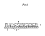
- FIG. 1 to 3 are each a cross sectional view illustrating the steps of sealing with a resin, a plurality of electronic elements that are mounted on a substrate. In the first place as illustrated on FIG.
- a dam frame is formed by sticking down a PSA sheet to edge and side portions of a substrate 1 loaded with a plurality of electronic elements 2. Subsequently as illustrated on FIG. 2, a resin for sealing 4 is poured in the inside of the dam frame, and then heat-cured the same.
- the resin for sealing and heat-curing conditions are not specifically limited, and there are applicable thereto, the resin for sealing and heat-curing conditions that are usually used for the purpose of this kind.
- the dam frame is substantially free from deformation even under heating, the cross sectional configuration thereof on FIG. 2 remains substantially unchanged.
- the base material layer is thinned by volume reduction under heating, whereby the dam frame 3 becomes lower than the height of the heat-cured resin for sealing 4 as illustrated on FIG. 3.
- the resin for sealing is heat-cured, and thereafter the elements are cut and separated into each unit electronic device by means of dicing.
- the thicknesses of the heat- cured resin for sealing sometimes include dispersion to some extent depending upon the portion and position, and it is preferable in this case to polish and smooth the surfaces of the cured resin for sealing prior to dicing.
- the dam frame becomes an obstacle to polishing, thereby necessitating to remove the same prior to the polishing.
- the dam frame is lower than the height of the heat-cured resin for sealing as illustrated on FIG. 3, the dam frame need not be removed.
- FIG. 1 to 3 which are each a cross sectional view illustrating the steps of sealing with a resin, a plurality of electronic elements that are mounted on a substrate, are substantially identical with the case of forming a dam frame on a substrate loaded with a single or a plurality of electronic elements individually for each of the electronic elements, pouring a resin for sealing in the inside of each of the dam frames, and heat-curing the poured resin, except for the difference of the dam frame being formed in a state of encompassing one electronic element.
- the dam frame In the case of forming the dam frame with the PSA sheet, it is preferable from the aspect of workability to stick down a PSA sheet which has been formed in advance into a prescribed shape (in the form of a window frame) to the substrate.
- the dam frame need only be formed so as to encompass the electronic element.
- the dam frame may be installed at a distance inwardly from the edge and side portions of a substrate.
- the process dispenses with intricate steps or a long time for the formation of the dam frame, thereby enables to produce a resin-sealed type electronic device with minimized number of production steps and a shortest time, and is particularly well suited for small lots and multi-item manufacture of electronic devices requiring sealing with a resin.
- the present invention will be described in more detail with reference to working examples.
- a dam frame was formed by sticking down a PSA sheet to edge and side portions of a substrate loaded with a plurality of electronic elements as illustrated on FIG.1.
- the substrate used therein was a ceramic substrate measuring 94 mm ⁇ 94 mm square and 1 mm in thickness, and 21 ⁇ 11 numbers of electronic elements measuring 3.0 mm ⁇ 7.0 mm and 400 ⁇ m in thickness were each arranged at an equal interval on the central portion of the substrate (80 mm ⁇ 80 mm square) excluding a width of 7.0 mm from each of the edge and side portions.
- the electronic elements were each subjected to bonding, and had a height of about 500 ⁇ m including bonding wires.
- the base material layer for the PSA sheet use was made of 3 mm thick polypropylene foam (manufactured by Sekisui Chemical Co., Ltd. under the trade name Softlon SP #2003 , closed cell type with an expansion ratio of 25).
- a releasing film made of 38 ⁇ m thick polyethylene terephthalate was coated on the releasing treatment face with an acrylic base PSA agent of permanent adhesion type (butyl acrylate / 2-hydroxyethyl acrylate being 91 / 9 parts by weight and isocyanate based cross-linking agent being 2.2 parts by weight) so that the dry layer thickness is made to be 20 ⁇ m.
- the resultant coated film on the PSA layer side was laminated on one side of the above base material layer to prepare a PSA sheet.
- the resultant PSA sheet was punched into a shape of window frame containing an outer frame measuring 84 mm ⁇ 84 mm square with 2 mm in width, and an inner frame measuring 80 mm ⁇ 80 mm square with 2 mm in width to prepare a dam frame.
- the dam frame thus obtained was, after removing the releasing film, stuck down to the above-mentioned ceramic substrate so that the centers of the substrate and dam frame coincided with each other. (The dam frame was installed at an equal distance inwardly from the edge and side portions of the substrate.)
- a resin for sealing (manufactured by Sumitomo Bakelite Co., Ltd. under the trade name: CRP-3150) was poured in the inside of the dam frame thus formed up to a thickness of 2 mm so as to result in the state as illustrated on FIG. 2. Subsequently the dam frame with the resin was placed in a curing oven, and heated at 175°C for 5 hours to cure the resin for sealing.
- the dam frame was thinned to a height of 1 mm or less due to volume reduction, and was made lower than the thickness of the cured resin for sealing (1.8 to 2.0 mm). Accordingly the surfaces of the cured resin for sealing were polished and smoothed without removing the dam frame. Thereafter the product was cut and separated into each of unit electronic device by means of dicing. The dicing was put into practice through a definite method by sticking the device and fixing to a dicing tape.
- Example 1 The procedure in Example 1 was repeated to obtain electronic devices except that in a PSA sheet, use was made of a base material layer composed of 3 mm thick polyethylene foam (manufactured by Sekisui Chemical Co., Ltd. under the trade name Softlon NF #3003, closed cell type with an expansion ratio of 30).
- a base material layer composed of 3 mm thick polyethylene foam (manufactured by Sekisui Chemical Co., Ltd. under the trade name Softlon NF #3003, closed cell type with an expansion ratio of 30).
- Example 1 The procedure in Example 1 was repeated to obtain electronic devices except that in a PSA sheet, use was made of a base material layer composed of 3 mm thick polyurethane foam (manufactured by Toyo Quality One Co., Ltd. under the trade name C-lite N-2830G, open cell type).
- a base material layer composed of 3 mm thick polyurethane foam (manufactured by Toyo Quality One Co., Ltd. under the trade name C-lite N-2830G, open cell type).
- a PSA sheet use was made of a base material layer composed of 3 mm thick non-foamed polyvinyl chloride sheet (manufactured by Mitsubishi Chemical MKV Company. under the trade name: Vinycasheet).
- the PSA layer was a layer which had a dry film thickness of 20 ⁇ m and was composed of removable type acrylic base PSA agent having the following blending composition.
- Example 1 The procedure in Example 1 was repeated to prepare electronic devices except that in a PSA sheet, use was made of a hardenable PSA agent having the following blending composition.
Landscapes
- Encapsulation Of And Coatings For Semiconductor Or Solid State Devices (AREA)
- Casting Or Compression Moulding Of Plastics Or The Like (AREA)
Applications Claiming Priority (2)
| Application Number | Priority Date | Filing Date | Title |
|---|---|---|---|
| JP2003342932A JP4152855B2 (ja) | 2003-10-01 | 2003-10-01 | 樹脂封止型の電子デバイスの製造方法。 |
| JP2003342932 | 2003-10-01 |
Publications (3)
| Publication Number | Publication Date |
|---|---|
| EP1521304A2 true EP1521304A2 (de) | 2005-04-06 |
| EP1521304A3 EP1521304A3 (de) | 2006-10-11 |
| EP1521304B1 EP1521304B1 (de) | 2010-12-29 |
Family
ID=34309103
Family Applications (1)
| Application Number | Title | Priority Date | Filing Date |
|---|---|---|---|
| EP04104575A Expired - Lifetime EP1521304B1 (de) | 2003-10-01 | 2004-09-21 | Verfahren zur Herstellung einer in Harz eingebetteten elektronischen Vorrichtung |
Country Status (6)
| Country | Link |
|---|---|
| US (1) | US7135358B2 (de) |
| EP (1) | EP1521304B1 (de) |
| JP (1) | JP4152855B2 (de) |
| AT (1) | ATE493759T1 (de) |
| DE (1) | DE602004030752D1 (de) |
| SG (1) | SG110183A1 (de) |
Cited By (1)
| Publication number | Priority date | Publication date | Assignee | Title |
|---|---|---|---|---|
| CN102097340A (zh) * | 2010-12-14 | 2011-06-15 | 沈阳中光电子有限公司 | 用cob灌胶封装制作smd的方法 |
Families Citing this family (10)
| Publication number | Priority date | Publication date | Assignee | Title |
|---|---|---|---|---|
| US6947748B2 (en) | 2000-12-15 | 2005-09-20 | Adaptix, Inc. | OFDMA with adaptive subcarrier-cluster configuration and selective loading |
| JP2006100489A (ja) * | 2004-09-29 | 2006-04-13 | Ricoh Co Ltd | プリント基板及びそのプリント基板を用いた電子ユニット並びに樹脂流出防止用ダムの形成方法 |
| US7573851B2 (en) | 2004-12-07 | 2009-08-11 | Adaptix, Inc. | Method and system for switching antenna and channel assignments in broadband wireless networks |
| DE102005005750B4 (de) * | 2005-02-07 | 2009-06-04 | Infineon Technologies Ag | Verfahren zum Verbinden eines thermoplastischen Materials mit einem duroplastischen Material und Thermoplast-Duroplast-Verbund |
| TWI421982B (zh) * | 2008-11-21 | 2014-01-01 | 先進封裝技術私人有限公司 | 半導體導線元件及其製造方法 |
| JP5263009B2 (ja) * | 2009-06-02 | 2013-08-14 | 株式会社村田製作所 | 基板の製造方法 |
| JP2013058330A (ja) * | 2011-09-07 | 2013-03-28 | Sumitomo Wiring Syst Ltd | シールド線のコネクタ接続端末処理構造部及びシールド線のコネクタ接続端末処理構造部の製造方法 |
| EP2780344A1 (de) | 2011-11-15 | 2014-09-24 | Xention Limited | Thieno[2,3-c]pyrazole als kaliumkanalinhibitoren |
| JP2016162964A (ja) * | 2015-03-04 | 2016-09-05 | ローム株式会社 | 半導体装置の製造方法および半導体装置 |
| CN106876342A (zh) * | 2016-12-19 | 2017-06-20 | 杰群电子科技(东莞)有限公司 | 一种双面散热半导体元件的制造方法 |
Family Cites Families (10)
| Publication number | Priority date | Publication date | Assignee | Title |
|---|---|---|---|---|
| US5612513A (en) * | 1995-09-19 | 1997-03-18 | Micron Communications, Inc. | Article and method of manufacturing an enclosed electrical circuit using an encapsulant |
| JPH09301480A (ja) * | 1996-05-13 | 1997-11-25 | Hitachi Ltd | 搬送用トレイ |
| US5776798A (en) * | 1996-09-04 | 1998-07-07 | Motorola, Inc. | Semiconductor package and method thereof |
| JP3819574B2 (ja) * | 1997-12-25 | 2006-09-13 | 三洋電機株式会社 | 半導体装置の製造方法 |
| US6130473A (en) * | 1998-04-02 | 2000-10-10 | National Semiconductor Corporation | Lead frame chip scale package |
| US6580159B1 (en) * | 1999-11-05 | 2003-06-17 | Amkor Technology, Inc. | Integrated circuit device packages and substrates for making the packages |
| US6444499B1 (en) * | 2000-03-30 | 2002-09-03 | Amkor Technology, Inc. | Method for fabricating a snapable multi-package array substrate, snapable multi-package array and snapable packaged electronic components |
| DE10024336A1 (de) * | 2000-05-17 | 2001-11-22 | Heidenhain Gmbh Dr Johannes | Bauelementanordnung und Verfahren zur Herstellung einer Bauelementanordnung |
| JP2003142634A (ja) * | 2001-08-20 | 2003-05-16 | Sony Corp | 半導体装置、その製造方法及び電子機器 |
| JP2003218251A (ja) * | 2002-01-28 | 2003-07-31 | Murata Mfg Co Ltd | 電子デバイスおよびその製造方法 |
-
2003
- 2003-10-01 JP JP2003342932A patent/JP4152855B2/ja not_active Expired - Lifetime
-
2004
- 2004-09-21 DE DE602004030752T patent/DE602004030752D1/de not_active Expired - Lifetime
- 2004-09-21 AT AT04104575T patent/ATE493759T1/de not_active IP Right Cessation
- 2004-09-21 EP EP04104575A patent/EP1521304B1/de not_active Expired - Lifetime
- 2004-09-24 US US10/948,164 patent/US7135358B2/en not_active Expired - Lifetime
- 2004-10-01 SG SG200405591A patent/SG110183A1/en unknown
Non-Patent Citations (1)
| Title |
|---|
| None |
Cited By (1)
| Publication number | Priority date | Publication date | Assignee | Title |
|---|---|---|---|---|
| CN102097340A (zh) * | 2010-12-14 | 2011-06-15 | 沈阳中光电子有限公司 | 用cob灌胶封装制作smd的方法 |
Also Published As
| Publication number | Publication date |
|---|---|
| SG110183A1 (en) | 2005-04-28 |
| EP1521304B1 (de) | 2010-12-29 |
| US20050074922A1 (en) | 2005-04-07 |
| EP1521304A3 (de) | 2006-10-11 |
| US7135358B2 (en) | 2006-11-14 |
| JP2005109300A (ja) | 2005-04-21 |
| ATE493759T1 (de) | 2011-01-15 |
| JP4152855B2 (ja) | 2008-09-17 |
| DE602004030752D1 (de) | 2011-02-10 |
Similar Documents
| Publication | Publication Date | Title |
|---|---|---|
| EP1521304B1 (de) | Verfahren zur Herstellung einer in Harz eingebetteten elektronischen Vorrichtung | |
| US6312800B1 (en) | Pressure sensitive adhesive sheet for producing a chip | |
| KR101043486B1 (ko) | 기판의 첩부방법 | |
| JP5718005B2 (ja) | 半導体装置製造用耐熱性粘着テープ及びそのテープを用いた半導体装置の製造方法。 | |
| EP1681713A1 (de) | Oberflächenschutzfilm und halbleiterwafer-lapping-verfahren | |
| US20080182363A1 (en) | Method for forming a microelectronic assembly including encapsulating a die using a sacrificial layer | |
| JP3553551B2 (ja) | 半導体ウェハを用いた半導体装置の製造方法 | |
| US20030228836A1 (en) | Subpad having robust, sealed edges | |
| GB2320615A (en) | A pressure sensitive adhesive sheet for dicing objects | |
| KR20180011178A (ko) | 전자 부품 보호 필름, 전자 부품 보호 부재, 전자 부품의 제조 방법 및 패키지의 제조 방법 | |
| JP3763710B2 (ja) | 防塵用カバーフィルム付きウエハ支持台及びその製造方法 | |
| US7063765B2 (en) | Adhesive sheet for affixation of a wafer and method for processing using the same | |
| US20130244377A1 (en) | Heat-resistant pressure-sensitive adhesive tape for production of semiconductor device and method for producing semiconductor device using the tape | |
| JP4881597B2 (ja) | 固体撮像装置の切断方法 | |
| EP2639278A1 (de) | Hitzebeständiges druckempfindliches Klebeband zur Herstellung eines Halbleiterbauelements und Verfahren zur Herstellung von Halbleiterbauelementen unter Verwendung des Klebebandes | |
| JP2004253643A (ja) | 半導体チップの製造方法 | |
| EP0935288A2 (de) | Versiegelte Anordnung für eine Halbleiterschaltung und deren Herstellungsverfahren | |
| JP2851808B2 (ja) | 研磨用ウエハ保持部材及びそのウエハ保持部材の定盤への装着方法 | |
| JPH0817855A (ja) | 半導体装置の製造方法およびこれに用いられる積層体 | |
| JP2007088292A (ja) | 板状部材の切断方法 | |
| JPH1086231A (ja) | プラスチックレンズの製造方法 | |
| JP2004031844A (ja) | 半導体素子の製造方法及び半導体素子の製造装置 | |
| TWI906443B (zh) | 半導體晶片的製造方法 | |
| KR20200112831A (ko) | 장척 적층 시트 및 그 권수체 | |
| KR101132346B1 (ko) | 팬 아웃형 웨이퍼 레벨 패키지용 점착제 조성물 및 이를 이용한 점착테이프 |
Legal Events
| Date | Code | Title | Description |
|---|---|---|---|
| PUAI | Public reference made under article 153(3) epc to a published international application that has entered the european phase |
Free format text: ORIGINAL CODE: 0009012 |
|
| AK | Designated contracting states |
Kind code of ref document: A2 Designated state(s): AT BE BG CH CY CZ DE DK EE ES FI FR GB GR HU IE IT LI LU MC NL PL PT RO SE SI SK TR |
|
| AX | Request for extension of the european patent |
Extension state: AL HR LT LV MK |
|
| PUAL | Search report despatched |
Free format text: ORIGINAL CODE: 0009013 |
|
| AK | Designated contracting states |
Kind code of ref document: A3 Designated state(s): AT BE BG CH CY CZ DE DK EE ES FI FR GB GR HU IE IT LI LU MC NL PL PT RO SE SI SK TR |
|
| AX | Request for extension of the european patent |
Extension state: AL HR LT LV MK |
|
| 17P | Request for examination filed |
Effective date: 20070215 |
|
| AKX | Designation fees paid |
Designated state(s): AT DE |
|
| RIN1 | Information on inventor provided before grant (corrected) |
Inventor name: SUGINO, TAKASHI Inventor name: SHINODA, TOMONORI |
|
| 17Q | First examination report despatched |
Effective date: 20071113 |
|
| GRAP | Despatch of communication of intention to grant a patent |
Free format text: ORIGINAL CODE: EPIDOSNIGR1 |
|
| RIC1 | Information provided on ipc code assigned before grant |
Ipc: H01L 23/24 20060101ALI20100611BHEP Ipc: H01L 21/56 20060101ALI20100611BHEP Ipc: H01L 23/31 20060101AFI20100611BHEP |
|
| GRAS | Grant fee paid |
Free format text: ORIGINAL CODE: EPIDOSNIGR3 |
|
| GRAA | (expected) grant |
Free format text: ORIGINAL CODE: 0009210 |
|
| AK | Designated contracting states |
Kind code of ref document: B1 Designated state(s): AT DE |
|
| REF | Corresponds to: |
Ref document number: 602004030752 Country of ref document: DE Date of ref document: 20110210 Kind code of ref document: P |
|
| REG | Reference to a national code |
Ref country code: DE Ref legal event code: R096 Ref document number: 602004030752 Country of ref document: DE Effective date: 20110210 |
|
| PG25 | Lapsed in a contracting state [announced via postgrant information from national office to epo] |
Ref country code: AT Free format text: LAPSE BECAUSE OF FAILURE TO SUBMIT A TRANSLATION OF THE DESCRIPTION OR TO PAY THE FEE WITHIN THE PRESCRIBED TIME-LIMIT Effective date: 20101229 |
|
| PLBE | No opposition filed within time limit |
Free format text: ORIGINAL CODE: 0009261 |
|
| STAA | Information on the status of an ep patent application or granted ep patent |
Free format text: STATUS: NO OPPOSITION FILED WITHIN TIME LIMIT |
|
| 26N | No opposition filed |
Effective date: 20110930 |
|
| REG | Reference to a national code |
Ref country code: DE Ref legal event code: R097 Ref document number: 602004030752 Country of ref document: DE Effective date: 20110930 |
|
| PGFP | Annual fee paid to national office [announced via postgrant information from national office to epo] |
Ref country code: DE Payment date: 20220803 Year of fee payment: 19 |
|
| REG | Reference to a national code |
Ref country code: DE Ref legal event code: R119 Ref document number: 602004030752 Country of ref document: DE |
|
| PG25 | Lapsed in a contracting state [announced via postgrant information from national office to epo] |
Ref country code: DE Free format text: LAPSE BECAUSE OF NON-PAYMENT OF DUE FEES Effective date: 20240403 |