EP1525621B1 - Méthode d'opération d'un dispositif semi-conducteur à grille en tranchée - Google Patents
Méthode d'opération d'un dispositif semi-conducteur à grille en tranchée Download PDFInfo
- Publication number
- EP1525621B1 EP1525621B1 EP03725542A EP03725542A EP1525621B1 EP 1525621 B1 EP1525621 B1 EP 1525621B1 EP 03725542 A EP03725542 A EP 03725542A EP 03725542 A EP03725542 A EP 03725542A EP 1525621 B1 EP1525621 B1 EP 1525621B1
- Authority
- EP
- European Patent Office
- Prior art keywords
- region
- drain
- gate
- trench
- field plate
- Prior art date
- Legal status (The legal status is an assumption and is not a legal conclusion. Google has not performed a legal analysis and makes no representation as to the accuracy of the status listed.)
- Expired - Lifetime
Links
Images


Classifications
-
- H—ELECTRICITY
- H10—SEMICONDUCTOR DEVICES; ELECTRIC SOLID-STATE DEVICES NOT OTHERWISE PROVIDED FOR
- H10D—INORGANIC ELECTRIC SEMICONDUCTOR DEVICES
- H10D30/00—Field-effect transistors [FET]
- H10D30/60—Insulated-gate field-effect transistors [IGFET]
- H10D30/64—Double-diffused metal-oxide semiconductor [DMOS] FETs
- H10D30/66—Vertical DMOS [VDMOS] FETs
- H10D30/668—Vertical DMOS [VDMOS] FETs having trench gate electrodes, e.g. UMOS transistors
-
- H—ELECTRICITY
- H10—SEMICONDUCTOR DEVICES; ELECTRIC SOLID-STATE DEVICES NOT OTHERWISE PROVIDED FOR
- H10D—INORGANIC ELECTRIC SEMICONDUCTOR DEVICES
- H10D12/00—Bipolar devices controlled by the field effect, e.g. insulated-gate bipolar transistors [IGBT]
- H10D12/411—Insulated-gate bipolar transistors [IGBT]
- H10D12/441—Vertical IGBTs
- H10D12/461—Vertical IGBTs having non-planar surfaces, e.g. having trenches, recesses or pillars in the surfaces of the emitter, base or collector regions
- H10D12/481—Vertical IGBTs having non-planar surfaces, e.g. having trenches, recesses or pillars in the surfaces of the emitter, base or collector regions having gate structures on slanted surfaces, on vertical surfaces, or in grooves, e.g. trench gate IGBTs
-
- H—ELECTRICITY
- H10—SEMICONDUCTOR DEVICES; ELECTRIC SOLID-STATE DEVICES NOT OTHERWISE PROVIDED FOR
- H10D—INORGANIC ELECTRIC SEMICONDUCTOR DEVICES
- H10D30/00—Field-effect transistors [FET]
- H10D30/60—Insulated-gate field-effect transistors [IGFET]
- H10D30/64—Double-diffused metal-oxide semiconductor [DMOS] FETs
- H10D30/65—Lateral DMOS [LDMOS] FETs
- H10D30/658—Lateral DMOS [LDMOS] FETs having trench gate electrodes
-
- H—ELECTRICITY
- H10—SEMICONDUCTOR DEVICES; ELECTRIC SOLID-STATE DEVICES NOT OTHERWISE PROVIDED FOR
- H10D—INORGANIC ELECTRIC SEMICONDUCTOR DEVICES
- H10D64/00—Electrodes of devices having potential barriers
- H10D64/111—Field plates
- H10D64/117—Recessed field plates, e.g. trench field plates or buried field plates
-
- H—ELECTRICITY
- H10—SEMICONDUCTOR DEVICES; ELECTRIC SOLID-STATE DEVICES NOT OTHERWISE PROVIDED FOR
- H10W—GENERIC PACKAGES, INTERCONNECTIONS, CONNECTORS OR OTHER CONSTRUCTIONAL DETAILS OF DEVICES COVERED BY CLASS H10
- H10W70/00—Package substrates; Interposers; Redistribution layers [RDL]
- H10W70/40—Leadframes
- H10W70/481—Leadframes for devices being provided for in groups H10D8/00 - H10D48/00
-
- H—ELECTRICITY
- H10—SEMICONDUCTOR DEVICES; ELECTRIC SOLID-STATE DEVICES NOT OTHERWISE PROVIDED FOR
- H10W—GENERIC PACKAGES, INTERCONNECTIONS, CONNECTORS OR OTHER CONSTRUCTIONAL DETAILS OF DEVICES COVERED BY CLASS H10
- H10W90/00—Package configurations
- H10W90/811—Multiple chips on leadframes
-
- H—ELECTRICITY
- H10—SEMICONDUCTOR DEVICES; ELECTRIC SOLID-STATE DEVICES NOT OTHERWISE PROVIDED FOR
- H10D—INORGANIC ELECTRIC SEMICONDUCTOR DEVICES
- H10D30/00—Field-effect transistors [FET]
- H10D30/60—Insulated-gate field-effect transistors [IGFET]
- H10D30/63—Vertical IGFETs
- H10D30/635—Vertical IGFETs having no inversion channels, e.g. vertical accumulation channel FETs [ACCUFET] or normally-on vertical IGFETs
-
- H—ELECTRICITY
- H10—SEMICONDUCTOR DEVICES; ELECTRIC SOLID-STATE DEVICES NOT OTHERWISE PROVIDED FOR
- H10D—INORGANIC ELECTRIC SEMICONDUCTOR DEVICES
- H10D64/00—Electrodes of devices having potential barriers
- H10D64/20—Electrodes characterised by their shapes, relative sizes or dispositions
- H10D64/27—Electrodes not carrying the current to be rectified, amplified, oscillated or switched, e.g. gates
- H10D64/311—Gate electrodes for field-effect devices
- H10D64/411—Gate electrodes for field-effect devices for FETs
- H10D64/511—Gate electrodes for field-effect devices for FETs for IGFETs
-
- H—ELECTRICITY
- H10—SEMICONDUCTOR DEVICES; ELECTRIC SOLID-STATE DEVICES NOT OTHERWISE PROVIDED FOR
- H10W—GENERIC PACKAGES, INTERCONNECTIONS, CONNECTORS OR OTHER CONSTRUCTIONAL DETAILS OF DEVICES COVERED BY CLASS H10
- H10W72/00—Interconnections or connectors in packages
- H10W72/071—Connecting or disconnecting
- H10W72/075—Connecting or disconnecting of bond wires
-
- H—ELECTRICITY
- H10—SEMICONDUCTOR DEVICES; ELECTRIC SOLID-STATE DEVICES NOT OTHERWISE PROVIDED FOR
- H10W—GENERIC PACKAGES, INTERCONNECTIONS, CONNECTORS OR OTHER CONSTRUCTIONAL DETAILS OF DEVICES COVERED BY CLASS H10
- H10W72/00—Interconnections or connectors in packages
- H10W72/50—Bond wires
- H10W72/541—Dispositions of bond wires
- H10W72/5449—Dispositions of bond wires not being orthogonal to a side surface of the chip, e.g. fan-out arrangements
-
- H—ELECTRICITY
- H10—SEMICONDUCTOR DEVICES; ELECTRIC SOLID-STATE DEVICES NOT OTHERWISE PROVIDED FOR
- H10W—GENERIC PACKAGES, INTERCONNECTIONS, CONNECTORS OR OTHER CONSTRUCTIONAL DETAILS OF DEVICES COVERED BY CLASS H10
- H10W72/00—Interconnections or connectors in packages
- H10W72/50—Bond wires
- H10W72/541—Dispositions of bond wires
- H10W72/547—Dispositions of multiple bond wires
- H10W72/5475—Dispositions of multiple bond wires multiple bond wires connected to common bond pads at both ends of the wires
-
- H—ELECTRICITY
- H10—SEMICONDUCTOR DEVICES; ELECTRIC SOLID-STATE DEVICES NOT OTHERWISE PROVIDED FOR
- H10W—GENERIC PACKAGES, INTERCONNECTIONS, CONNECTORS OR OTHER CONSTRUCTIONAL DETAILS OF DEVICES COVERED BY CLASS H10
- H10W72/00—Interconnections or connectors in packages
- H10W72/90—Bond pads, in general
- H10W72/921—Structures or relative sizes of bond pads
- H10W72/926—Multiple bond pads having different sizes
-
- H—ELECTRICITY
- H10—SEMICONDUCTOR DEVICES; ELECTRIC SOLID-STATE DEVICES NOT OTHERWISE PROVIDED FOR
- H10W—GENERIC PACKAGES, INTERCONNECTIONS, CONNECTORS OR OTHER CONSTRUCTIONAL DETAILS OF DEVICES COVERED BY CLASS H10
- H10W72/00—Interconnections or connectors in packages
- H10W72/90—Bond pads, in general
- H10W72/951—Materials of bond pads
-
- H—ELECTRICITY
- H10—SEMICONDUCTOR DEVICES; ELECTRIC SOLID-STATE DEVICES NOT OTHERWISE PROVIDED FOR
- H10W—GENERIC PACKAGES, INTERCONNECTIONS, CONNECTORS OR OTHER CONSTRUCTIONAL DETAILS OF DEVICES COVERED BY CLASS H10
- H10W90/00—Package configurations
-
- H—ELECTRICITY
- H10—SEMICONDUCTOR DEVICES; ELECTRIC SOLID-STATE DEVICES NOT OTHERWISE PROVIDED FOR
- H10W—GENERIC PACKAGES, INTERCONNECTIONS, CONNECTORS OR OTHER CONSTRUCTIONAL DETAILS OF DEVICES COVERED BY CLASS H10
- H10W90/00—Package configurations
- H10W90/701—Package configurations characterised by the relative positions of pads or connectors relative to package parts
- H10W90/751—Package configurations characterised by the relative positions of pads or connectors relative to package parts of bond wires
- H10W90/753—Package configurations characterised by the relative positions of pads or connectors relative to package parts of bond wires between laterally-adjacent chips
-
- H—ELECTRICITY
- H10—SEMICONDUCTOR DEVICES; ELECTRIC SOLID-STATE DEVICES NOT OTHERWISE PROVIDED FOR
- H10W—GENERIC PACKAGES, INTERCONNECTIONS, CONNECTORS OR OTHER CONSTRUCTIONAL DETAILS OF DEVICES COVERED BY CLASS H10
- H10W90/00—Package configurations
- H10W90/701—Package configurations characterised by the relative positions of pads or connectors relative to package parts
- H10W90/751—Package configurations characterised by the relative positions of pads or connectors relative to package parts of bond wires
- H10W90/756—Package configurations characterised by the relative positions of pads or connectors relative to package parts of bond wires between a chip and a stacked lead frame, conducting package substrate or heat sink
Definitions
- the present invention relates to trench-gate semiconductor devices, for example insulated-gate field effect power transistors (commonly termed “MOSFETs”), or insulated-gate bipolar transistors (commonly termed “IGBTs").
- MOSFETs insulated-gate field effect power transistors
- IGBTs insulated-gate bipolar transistors
- Such trench-gate semiconductor devices are known having a source region and a drain region of a first conductivity type which are separated by a channel-accommodating region adjacent to the gate.
- US-A-5998833 describes a vertical device of this type which includes a trench-based source electrode, between the gate electrode and the bottom of the trench.
- the trench-based source electrode is electrically connected to the source electrode of the device. It is provided with a view to improving the breakdown and high frequency switching characteristics of the device with minimal impact on its specific on-state resistance.
- EP-A-1170803 discloses a similar structure to that referred to above in relation to US-A-5998833 .
- a "shield gate” is located below the gate electrode, near the bottom of the trench and is connected to a constant voltage, such as ground.
- a shield gate is located below the gate electrode, near the bottom of the trench and is connected to a constant voltage, such as ground.
- the shield gate is connected to the source region.
- the same connection is disclosed in a similar structure also in WO-A-0213257 .
- the present invention relates to a trench-gate semiconductor device including:
- bulk breakdown voltage is used herein to refer to the maximum voltage per micrometer which may be withstood without avalanche breakdown by a one-sided abrupt 1D p-n junction formed using semiconductor material of a given doping level at room temperature.
- connection of such an insulated field plate to a potential close to the bulk breakdown voltage of the drain drift region causes the potential drop across the drain drift region to be spread considerably more evenly particularly at applied voltages greater than the bulk breakdown voltage, thereby substantially increasing the breakdown voltage of the device.
- This enables a higher level of doping to be used in the drain drift region relative to a device without the field plate having the same breakdown characteristics, thereby providing devices with a lower specific on-state resistance.
- the presence of the field plate reduces the gate-to-drain capacitance of the device. It therefore improves its switching speed and reduces the amount of power loss occurring during switching by reducing the amount of charge which flows to and from the gate. This is particularly beneficial in applications requiring high frequency switching.
- the trench and/or the field plate extend substantially to the junction between the drain drift region and the drain contact region, to optimise its ability to even out the electric field across the drain drift region.
- the trench and/or field plate extend up to the transition region between the drain drift and contact regions. If the trench and/or field plate extend into this transition region or beyond then field crowding at the corners of the trench may be increased.
- the device of the invention may be a vertical device, with the field plate located in the trench between the gate and the bottom of the trench. Alternatively, it may be a lateral device, the field plate being provided between the gate and a side wall of the trench.
- the present invention also relates to a module comprising a device having the configuration defined above along with one or more other semiconductor devices, wherein the field plate is conveniently connected to an internal voltage line of the module.
- an additional external terminal may be provided on the device (in the case of a discrete device) or the module which is electrically connected to the field plate. This enables a dedicated voltage level for the field plate to be applied.
- a bias potential to the field plate around 60 to 100% of the bulk breakdown voltage, of the drain drift region is preferable. More particularly, a bias potential of around 80% of the bulk breakdown voltage of the drain drift region is preferred, as it allows some tolerance of variations in the width of the transition region between the drain drift and contact regions which may lead to variations in the level of doping in the drain drift region around the bottom of the trench.
- the present invention provides a method of operating a trench-gate semiconductor device having a field plate in the trench as described herein, the method comprising connecting the field plate of the device to a bias potential greater than the gate potential and near to the bulk breakdown voltage of the drain drift region.
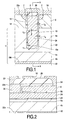
- Figure 1 illustrates an exemplary embodiment of a power semiconductor device in accordance with the invention.
- Source and drain regions 2 and 4 respectively of a first conductivity type (n-type in this example) are separated by a channel-accommodating region 6 of the opposite, second conductivity type (that is, p-type in this example).
- Figure 1 shows a vertical device structure in which region 4a may be a drain drift region formed by an epitaxial layer of high resistivity (low doping) on a substrate, drain contact region 4b of relatively high conductivity.
- the drain drift and contact regions 4a and 4b form a junction 4c therebetween.
- the drain contact region 4b may be of the same conductivity type (n-type in this example) as the region 4a to provide a vertical MOSFET, or it may be of opposite conductivity type (p-type in this example) to provide a vertical IGBT.
- a gate 8 is present in a trench 10 which extends through the regions 2 and 6 and into an underlying portion of the drain drift region 4a.
- the application of a voltage signal to the gate 8 in the on-state of the device serves in known manner to induce a conduction channel 16 in the region 6 and to control current flow in this conduction channel 16 between the source and drain regions 2 and 4.
- the source region 2 is contacted by a source electrode 18 in the case of a MOSFET at the top major surface 20a of the device semiconductor body 20 (typically of monocrystalline silicon).
- the drain contact region 4b is contacted by an electrode 22, called the drain electrode in the case of a MOSFET, at the bottom major surface 20b of the device semiconductor body 20.
- the source and drain electrodes 18 and 22 are known as the emitter and collector, respectively, in an IGBT.
- a field plate 24 is provided in the trench 10, between the gate 8 and the bottom 10a of the trench.
- the field plate is preferably formed of doped polycrystalline silicon of the first conductivity type. Alternatively, it may be made of metal, for example.
- Both the field plate 24 and the gate 8 are insulated from each other and from the source electrode 28 and surrounding semiconductor body 20 by insulating material 26. This layer may consist of silicon dioxide, for example.
- the trench 10 and field plate 24 extend into the semiconductor body 20 to a depth close to the junction 4c between the drain drift and contact regions, 4a and 4b.
- the trench 10 extends to a depth immediately above the transition region.
- the field plate 24 is spaced from the bottom of the trench by a layer of insulating material 26 of thickness t1. Similarly, it is spaced from the gate by a layer of insulating material 26 of thickness t2.
- the side walls of the gate and field plate are insulated from the semiconductor body by layers of insulating material 26 of thickness t3 and t4, respectively.
- Thicknesses t3 and t4 may be of the order of 38nm, whilst t1 may be of the order of 0.2 micrometer, for example.
- a relatively thick layer is desirable below the field plate (ie. t1), particularly for higher levels of doping in the drain drift region 4a, so that it is able to withstand the high electric fields produced at the corners of the trench.
- Thickness t2 is preferably greater than t3 and t4.
- a bias potential near to the bulk breakdown voltage of the drain drift region 4a is applied to the field plate 24. Therefore it is advantageous to have a relatively thick insulating layer (of the order of 0.2 micrometer, or example) between the field plate and the gate to withstand the potential difference therebetween.
- Low doped drain drift region 4a may typically be grown as an epitaxial layer of the first conductivity type.
- the doping concentration of the drift region may be substantially uniform throughout its depth. Nevertheless, it may be preferable to vary the concentration across the drift region. In particular, providing a doping profile with the concentration decreasing (for example in a linear manner) in the direction from the drain contact region 4b towards the channel-accommodating region 6 may reduce the on-resistance of the device.
- Figure 2 shows a cross-section through the device of Figure 1 , along line A-A. It illustrates an example of how a connection to the field plate 24 may be made from outside the semiconductor body 20, independently of the gate and source electrode.
- Doped polycrystalline silicon contact layer 30 is provided towards one end of the trench 10 and is electrically connected to the field plate 24. It extends from the field plate to the top major surface 20a of the device semiconductor body 20, where it is contacted by a field plate contact electrode 32.
- the gate 8 is electrically connected to a gate contact electrode 34 towards the other end of the trench 10.
- EP-A-1170803 with reference to Figures 9 to 13 thereof is an example of a suitable method of manufacturing a device embodying the present invention, except for the step of patterning a metal layer to provide contact electrodes on the semiconductor body.
- the metal layer should be patterned to provide three separate contact electrodes shown in present Figure 2 , namely source electrode 18, field plate contact electrode 32, and gate contact electrode 34.
- Figure 3 shows a cross-section through a further embodiment of the invention, similar to that of Figure 1 .
- the embodiment of Figure 3 differs from that of Figure 1 in that the gate 8 is shallower than the upper boundary 14 of the drain drift region 4a adjacent the trench 10 in Figure 3 , whereas in Figure 1 , the gate 8 extends below this boundary beyond the channel-accommodating region, into the drain drift region.
- the field plate 24 may extend above the drain drift region boundary 14 to enhance its shielding of the gate from the drain drift region.
- the bias potential connected to the field plate is sufficient to induce a channel alongside the field plate, such that in the on-state, simultaneous operation of the gate 8 and biasing of the field plate causes a conduction channel 16 to be formed between the source and drain regions of the device which extends alongside both the gate and the field plate.
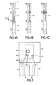
- Figures 4A to 4C are cross-sectional views of a portion of a transistor cell area of a semiconductor body embodying the present invention, which illustrate the beneficial effect that the field plate biased close to the bulk breakdown voltage of the drain drift region has on the device breakdown characteristics.
- Simulated lines of equal potential are shown by solid lines.
- the simulations are based on the use of silicon with a bulk breakdown voltage of around 30V.
- the views 4A to 4C show the potential distribution in the forward blocking mode at the onset of breakdown, with the field plate 24 held at 0, 29 and 33V respectively.
- the extent of the depletion region in each case is indicated by dashed lines.
- the distance d from the to major surface of the device semiconductor body is indicated in micrometers.
- FIG. 5 shows an internal plan view of the packaging of a discrete device in accordance with an embodiment of the invention.
- a MOSFET die 40 has a gate bond pad 42 connected to its gate contact electrode, a source bond pad 48 connected to its source contact electrode, and a field plate bond pad 44 connected to its field plate contact electrode for applying an independent bias thereto.
- the MOSFET is mounted on a drain pad 46, which is electrically connected to the drain electrode 22 on the bottom major surface of the MOSFET die.
- Bond wires 50 connect the bond pads 42, 44, 48 to respective terminals or pins 52, 54 and 58. Drain pad 46 directly contacts the respective pin 56.
- the packaging may be completed in a known manner.
- a semiconductor device as described above is included in a module, with its field plate(s) connected to an internal voltage line or level of the module.
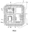
- Figure 6 shows an internal plan view of the packaging of a module 60 including two semiconductor devices having biased field plates of the form described above.
- the module is a DC-DC converter, for use as a VRM in a PC motherboard, for example.
- a known DC-DC converter circuit and its operation are described in US-B-6175225 of the present applicant (our ref. PHB34370).
- the configuration shown in Figure 6 is a modified implementation of the circuit shown in Figure 3 of US-B-6175225 .
- the module of Figure 6 includes a control MOSFET 62, a "sync" MOSFET 64, and a driver IC 66.
- the MOSFETs correspond to first and second switches 5 and 6 of Figure 3 of US-B-6175225 , respectively. They are connected in series between a DC input, V DD , and ground, V SS . The switches are closed alternately in response to a switching signal, PWM IN , which is inputted to driver IC 66. The further operation of a circuit of this type is described in US-B-6175225 .
- each MOSFET 62, 64 includes a field plate bond pad 68 which is connected to the respective field plate contact electrode of each MOSFET.
- the field plate bond pad of sync MOSFET 64 is connected to the power supply voltage, V CC , via the driver IC, for example, which may typically be 5 or 12V.
- V CC power supply voltage
- the gate drive to the control MOSFET (“first switch 5") is via a boost or reservoir capacitor 37 connected between a boost terminal 33 and Vout.
- the field plate bond pad of control MOSFET 62 would be connected to boost terminal 33.
- the silicon selected for the MOSFETs 62 and 64 may have a bulk breakdown voltage of around 15V or more, for example.
- a vertical trench-gate device has been described with reference to Figures 1 to 4 hereof.
- a lateral trench-gate device is also possible in accordance with the invention, and a cross-sectional perspective view of an embodiment thereof is shown in Figure 7 .
- Source and drain electrodes are omitted from the Figure in the interests of clarity.
- the field plate 24 is provided in the trench 10 between the gate 8 and the drain contact region 4b as before, but in this case, it is located alongside rather than below the gate to modulate the electric field distribution across the drain drift region 4a of the device.
- the device is fabricated on a substrate 70, highly doped with the opposite, second conductivity type dopant (that is, p-type in the examples described herein).
- the gate 8 is shown in Figure 7 as extending into the drain drift region 4a, in another preferred embodiment, the gate does not extend beyond the channel-accommodating region 6, in a similar manner to the embodiment of Figure 3 . Instead the gate is laterally spaced from the boundary of the drain drift region. As in the Figure 3 embodiment, this serves to reduce further the gate-to-drain capacitance of the device.
- n-channel devices in which the source and drain regions 2 and 4 are of n-type conductivity, the channel-accommodating body region 6 is of p-type conductivity, and an electron inversion channel 16 is induced in the region 6 by the gate 8.
- a p-channel device can be made. In that case, regions 2 and 4 are of p-type, the region 6 and substrate 70 are of n-type, and a hole inversion channel is induced in the region 6 by the gate 8.
- an accumulation-mode device may be manufactured in accordance with the invention.
- Such a device of the p-channel type has p-type source and drain regions 2 and 4, and a p-type channel-accommodating region 6. It may also have an n-type deep localised region within each cell.
- N-type polycrystalline silicon may be used for the gate 8.
- a hole accumulation channel 16 is induced in the region 6 by the gate 8 in the on-state.
- the low-doped p-type region 6 may be wholly depleted in the off-state, by depletion layers from the insulated gate 8 and from the deep n-type region.
- the trench 10 extends in the semiconductor body close to the junction between the drain drift region 4a and the drain contact region 4b. It will be appreciated that the extent of the trench towards the drain contact region may be reduced whilst still providing benefits in terms of the improved breakdown properties of the device, and reduced gate-to-drain capacitance.
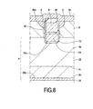
- the trench 10 is relatively shallow, and only extends a small proportion of the distance across the drain drift region 4a towards the drain contact region 4b.
- the gate 8 in the structure of Figure 8 does not extend into the drain drift region 4a, that is, it is shallower than the upper boundary of the drain drift region adjacent the trench 10.
- the field plate or lower electrode 24 in the trench below the gate extends into the channel accommodating region 6.
- this bias potential should be greater than the gate threshold voltage to ensure that a channel is induced alongside the field plate or lower electrode in the on-state of the device.
- a novel trench-gate semiconductor device including a semiconductor body defining a trench having an insulated gate therein, the semiconductor body comprising a source region and a drain region of a first conductivity type which are separated by a channel-accommodating region adjacent to the gate, the drain region comprising a drain drift region and a drain contact region, with the drain drift region between the channel-accommodating region and the drain contact region, and the drain drift region doped to a lesser extent than the drain contact region, and an insulated lower electrode in the trench between the gate and the drain contact region, wherein the lower electrode is for connection to a bias potential at least equal to the gate potential and lower than the bulk breakdown voltage of the drain drift region, the gate is shallower than the upper boundary of the drain drift region adjacent the trench, and the field plate extends above the upper boundary.
- a vertical discrete device has been illustrated with reference to Figures 1 to 4 , having its drain electrode 22 contacting the region 4b at the back surface 20b of the body 20.
- the region 4b may be a doped buried layer between a device substrate and the epitaxial low-doped drain region 4a.
- This buried layer region 4b may be contacted by an electrode at the front major surface 20a, via a doped peripheral contact region which extends from the surface 20a to the depth of the buried layer.
- Semiconductor materials other than silicon may be used for devices in accordance with the invention, for example, silicon carbide.
- FIG. 1 shows only one cell, but typically the device comprises many hundreds of these parallel cells between the electrodes 18 and 22. Similary, only one cell is shown in Figures 7 for the purposes of illustration.
Landscapes
- Electrodes Of Semiconductors (AREA)
- Insulated Gate Type Field-Effect Transistor (AREA)
Abstract
Claims (7)
- Procédé de fonctionnement d'un dispositif à semi-conducteur à grille en tranchée, le dispositif à semi-conducteur à grille en tranchée comprenant :un corps de semi-conducteur (20) définissant une tranchée (10) contenant une grille isolée (8), le corps de semi-conducteur comprenant une région de source (2) et une région de drain (4) d'un premier type de conductivité qui sont séparées par une région accueillant un canal (6) adjacente à la grille, la région de drain comprenant une région de dérive de drain (4a) et une région de contact de drain (4b), avec la région de dérive de drain entre la région accueillant le canal (6) et la région de contact de drain (4b), et la région de dérive de drain (4a) étant dopée dans une moindre mesure que la région de contact de drain (4b) ; etune plaque de champ isolée (24) dans la tranchée (10) entre la grille (8) et la région de contact de drain (4b) ;le procédé étant caractérisé par le raccordement de la plaque de champ (24) à un potentiel de polarisation supérieur au potentiel de grille et proche de la tension de claquage en volume de la région de dérive de drain (4a), la tension de claquage en volume étant la tension maximale par micromètre que peut supporter, à température ambiante, sans claquage par avalanche une jonction p-n 1D à une seule face abrupte formée à l'aide du matériau semi-conducteur de la région de dérive de drain (4a).
- Procédé selon la revendication 1, dans lequel la tranchée (10) s'étend substantiellement jusqu'à la jonction (4c) entre la région de dérive de drain (4a) et la région de contact de drain (4b).
- Procédé selon la revendication 1 ou la revendication 2, dans lequel la grille (8) est moins profonde que la limite supérieure de la région de dérive de drain (4a) contre la tranchée (10), et dans lequel la plaque de champ (24) s'étend au-dessus de la limite supérieure.
- Procédé selon l'une quelconque des revendications précédentes, dans lequel le dispositif est inclus dans un module (60) et dans lequel la plaque de champ (24) est raccordée à une ligne de tension interne du module (60).
- Procédé selon l'une quelconque des revendications précédentes, dans lequel est disposée une borne externe supplémentaire (54) qui est raccordée électriquement à la plaque de champ (24).
- Procédé selon l'une quelconque des revendications précédentes, dans lequel le potentiel de polarisation est d'environ 60 à 100% de la tension de claquage en volume de la région de dérive de drain (4a).
- Procédé selon la revendication 6, dans lequel le potentiel de polarisation est d'environ 80% de la tension de claquage en volume de la région de dérive de drain (4a).
Applications Claiming Priority (5)
| Application Number | Priority Date | Filing Date | Title |
|---|---|---|---|
| GB0212564 | 2002-05-31 | ||
| GBGB0212564.9A GB0212564D0 (en) | 2002-05-31 | 2002-05-31 | Trench-gate semiconductor device |
| GBGB0228809.0A GB0228809D0 (en) | 2002-05-31 | 2002-12-11 | Trench-gate semiconductor devices |
| GB0228809 | 2002-12-11 | ||
| PCT/IB2003/002233 WO2003103056A2 (fr) | 2002-05-31 | 2003-05-21 | Dispositif semi-conducteur a tranchee/grille |
Publications (2)
| Publication Number | Publication Date |
|---|---|
| EP1525621A2 EP1525621A2 (fr) | 2005-04-27 |
| EP1525621B1 true EP1525621B1 (fr) | 2011-10-12 |
Family
ID=29713387
Family Applications (1)
| Application Number | Title | Priority Date | Filing Date |
|---|---|---|---|
| EP03725542A Expired - Lifetime EP1525621B1 (fr) | 2002-05-31 | 2003-05-21 | Méthode d'opération d'un dispositif semi-conducteur à grille en tranchée |
Country Status (5)
| Country | Link |
|---|---|
| US (1) | US7122860B2 (fr) |
| EP (1) | EP1525621B1 (fr) |
| JP (1) | JP2005528804A (fr) |
| AU (1) | AU2003228073A1 (fr) |
| WO (1) | WO2003103056A2 (fr) |
Families Citing this family (44)
| Publication number | Priority date | Publication date | Assignee | Title |
|---|---|---|---|---|
| US7638841B2 (en) * | 2003-05-20 | 2009-12-29 | Fairchild Semiconductor Corporation | Power semiconductor devices and methods of manufacture |
| DE10339455B3 (de) * | 2003-08-27 | 2005-05-04 | Infineon Technologies Ag | Vertikales Halbleiterbauelement mit einer eine Feldelektrode aufweisenden Driftzone und Verfahren zur Herstellung einer solchen Driftzone |
| GB0327792D0 (en) * | 2003-11-29 | 2003-12-31 | Koninkl Philips Electronics Nv | Trench insulated gate field effect transistor |
| TWI222685B (en) * | 2003-12-18 | 2004-10-21 | Episil Technologies Inc | Metal oxide semiconductor device and fabricating method thereof |
| US7405452B2 (en) * | 2004-02-02 | 2008-07-29 | Hamza Yilmaz | Semiconductor device containing dielectrically isolated PN junction for enhanced breakdown characteristics |
| US20050199918A1 (en) * | 2004-03-15 | 2005-09-15 | Daniel Calafut | Optimized trench power MOSFET with integrated schottky diode |
| JP2005340626A (ja) * | 2004-05-28 | 2005-12-08 | Toshiba Corp | 半導体装置 |
| DE102004029435B4 (de) * | 2004-06-18 | 2017-02-16 | Infineon Technologies Ag | Feldplattentrenchtransistor |
| JP5259920B2 (ja) * | 2004-08-04 | 2013-08-07 | ローム株式会社 | 半導体装置およびその製造方法 |
| DE102004044619B4 (de) * | 2004-09-13 | 2009-07-16 | Infineon Technologies Ag | Kondensatorstruktur in Grabenstrukturen von Halbleiterbauteilen und Halbleiterbauteile mit derartigen Kondensatorstrukturen und Verfahren zur Herstellung derselben |
| AT504998A2 (de) | 2005-04-06 | 2008-09-15 | Fairchild Semiconductor | Trenched-gate-feldeffekttransistoren und verfahren zum bilden derselben |
| JP4955222B2 (ja) | 2005-05-20 | 2012-06-20 | ルネサスエレクトロニクス株式会社 | 半導体装置の製造方法 |
| JP2008546189A (ja) | 2005-05-26 | 2008-12-18 | フェアチャイルド・セミコンダクター・コーポレーション | トレンチゲート電界効果トランジスタ及びその製造方法 |
| US7446374B2 (en) | 2006-03-24 | 2008-11-04 | Fairchild Semiconductor Corporation | High density trench FET with integrated Schottky diode and method of manufacture |
| DE102006026943B4 (de) * | 2006-06-09 | 2011-01-05 | Infineon Technologies Austria Ag | Mittels Feldeffekt steuerbarer Trench-Transistor mit zwei Steuerelektroden |
| DE102006030631B4 (de) * | 2006-07-03 | 2011-01-05 | Infineon Technologies Austria Ag | Halbleiterbauelementanordnung mit einem Leistungsbauelement und einem Logikbauelement |
| US7476932B2 (en) * | 2006-09-29 | 2009-01-13 | The Boeing Company | U-shape metal-oxide-semiconductor (UMOS) gate structure for high power MOS-based semiconductor devices |
| US8497549B2 (en) * | 2007-08-21 | 2013-07-30 | Fairchild Semiconductor Corporation | Method and structure for shielded gate trench FET |
| JP2009164558A (ja) * | 2007-12-10 | 2009-07-23 | Toyota Central R&D Labs Inc | 半導体装置とその製造方法、並びにトレンチゲートの製造方法 |
| US20100013009A1 (en) * | 2007-12-14 | 2010-01-21 | James Pan | Structure and Method for Forming Trench Gate Transistors with Low Gate Resistance |
| US7800176B2 (en) * | 2008-10-27 | 2010-09-21 | Infineon Technologies Austria Ag | Electronic circuit for controlling a power field effect transistor |
| US8198678B2 (en) | 2009-12-09 | 2012-06-12 | Infineon Technologies Austria Ag | Semiconductor device with improved on-resistance |
| JP6008377B2 (ja) * | 2010-03-03 | 2016-10-19 | ルネサスエレクトロニクス株式会社 | Pチャネル型パワーmosfet |
| JP5674530B2 (ja) * | 2010-09-10 | 2015-02-25 | ルネサスエレクトロニクス株式会社 | 半導体装置の制御装置 |
| JP2012204636A (ja) * | 2011-03-25 | 2012-10-22 | Toshiba Corp | 半導体装置およびその製造方法 |
| US8981748B2 (en) | 2011-08-08 | 2015-03-17 | Semiconductor Components Industries, Llc | Method of forming a semiconductor power switching device, structure therefor, and power converter |
| US8642425B2 (en) | 2012-05-29 | 2014-02-04 | Semiconductor Components Industries, Llc | Method of making an insulated gate semiconductor device and structure |
| US9202882B2 (en) | 2013-05-16 | 2015-12-01 | Infineon Technologies Americas Corp. | Semiconductor device with a thick bottom field plate trench having a single dielectric and angled sidewalls |
| JP2015142073A (ja) * | 2014-01-30 | 2015-08-03 | サンケン電気株式会社 | 半導体装置 |
| US9413348B2 (en) | 2014-07-29 | 2016-08-09 | Semiconductor Components Industries, Llc | Electronic circuit including a switch having an associated breakdown voltage and a method of using the same |
| JP2016063048A (ja) * | 2014-09-17 | 2016-04-25 | 富士電機株式会社 | トレンチ型絶縁ゲートバイポーラトランジスタ及びその製造方法 |
| JP2016163019A (ja) * | 2015-03-05 | 2016-09-05 | 株式会社東芝 | 半導体装置 |
| CN107636836B (zh) * | 2015-12-11 | 2020-11-27 | 富士电机株式会社 | 半导体装置 |
| DE102016103587B4 (de) * | 2016-02-29 | 2020-12-03 | Infineon Technologies Ag | Halbleitervorrichtung mit Hilfselektrodenpins |
| JP6830390B2 (ja) * | 2017-03-28 | 2021-02-17 | エイブリック株式会社 | 半導体装置 |
| JP7250473B2 (ja) * | 2018-10-18 | 2023-04-03 | 三菱電機株式会社 | 半導体装置 |
| FR3096832B1 (fr) | 2019-05-28 | 2022-05-13 | St Microelectronics Rousset | Structure de transistor |
| FR3106697A1 (fr) * | 2020-01-23 | 2021-07-30 | Stmicroelectronics (Rousset) Sas | Structure de transistor |
| EP4197026B1 (fr) * | 2020-08-13 | 2025-07-02 | Texas Instruments Incorporated | Procédé de fabrication de dispositif à semi-conducteur comprenant un isolateur latéral |
| WO2022036598A1 (fr) * | 2020-08-19 | 2022-02-24 | 华为技术有限公司 | Drmos, circuit intégré, dispositif électronique et procédé de fabrication |
| JP7394038B2 (ja) * | 2020-09-11 | 2023-12-07 | 株式会社東芝 | 半導体装置 |
| CN112349786B (zh) * | 2020-11-06 | 2022-07-29 | 中国电子科技集团公司第二十四研究所 | 介质共用的电阻场板场效应mos器件及其制备方法 |
| EP4167292A1 (fr) | 2021-10-15 | 2023-04-19 | Infineon Technologies Dresden GmbH & Co . KG | Dispositif à semiconducteurs |
| CN114709258B (zh) * | 2022-06-07 | 2022-08-30 | 深圳市威兆半导体股份有限公司 | 一种双沟道mosfet器件及其制造方法 |
Family Cites Families (7)
| Publication number | Priority date | Publication date | Assignee | Title |
|---|---|---|---|---|
| US5998833A (en) * | 1998-10-26 | 1999-12-07 | North Carolina State University | Power semiconductor devices having improved high frequency switching and breakdown characteristics |
| JP2003525003A (ja) * | 1999-07-02 | 2003-08-19 | コーニンクレッカ フィリップス エレクトロニクス エヌ ヴィ | Dc−dcコンバータ用スイッチング装置及びスイッチコンポーネント |
| EP1170803A3 (fr) | 2000-06-08 | 2002-10-09 | Siliconix Incorporated | MOSFET à grille en tranchée et sa méthode de fabrication |
| DE10038177A1 (de) | 2000-08-04 | 2002-02-21 | Infineon Technologies Ag | Mittels Feldeffekt steuerbares Halbleiterschaltelement mit zwei Steuerelektroden |
| DE10212149B4 (de) * | 2002-03-19 | 2007-10-04 | Infineon Technologies Ag | Transistoranordnung mit Schirmelektrode außerhalb eines aktiven Zellenfeldes und reduzierter Gate-Drain-Kapazität |
| DE10214175B4 (de) * | 2002-03-28 | 2006-06-29 | Infineon Technologies Ag | Mittels Feldeffekt steuerbares Halbleiterbauelement und Verfahren zu dessen Herstellung |
| CN100437942C (zh) * | 2002-05-31 | 2008-11-26 | Nxp股份有限公司 | 沟槽栅半导体器件及制造方法 |
-
2003
- 2003-05-21 AU AU2003228073A patent/AU2003228073A1/en not_active Abandoned
- 2003-05-21 EP EP03725542A patent/EP1525621B1/fr not_active Expired - Lifetime
- 2003-05-21 WO PCT/IB2003/002233 patent/WO2003103056A2/fr not_active Ceased
- 2003-05-21 JP JP2004510038A patent/JP2005528804A/ja not_active Withdrawn
- 2003-05-21 US US10/515,748 patent/US7122860B2/en not_active Expired - Lifetime
Also Published As
| Publication number | Publication date |
|---|---|
| WO2003103056A3 (fr) | 2004-02-05 |
| EP1525621A2 (fr) | 2005-04-27 |
| AU2003228073A8 (en) | 2003-12-19 |
| US20050173758A1 (en) | 2005-08-11 |
| JP2005528804A (ja) | 2005-09-22 |
| AU2003228073A1 (en) | 2003-12-19 |
| US7122860B2 (en) | 2006-10-17 |
| WO2003103056A2 (fr) | 2003-12-11 |
Similar Documents
| Publication | Publication Date | Title |
|---|---|---|
| EP1525621B1 (fr) | Méthode d'opération d'un dispositif semi-conducteur à grille en tranchée | |
| US7232726B2 (en) | Trench-gate semiconductor device and method of manufacturing | |
| US7719053B2 (en) | Semiconductor device having increased gate-source capacity provided by protruding electrode disposed between gate electrodes formed in a trench | |
| US7768064B2 (en) | Structure and method for improving shielded gate field effect transistors | |
| CN101889334B (zh) | 具有集成肖特基的高密度fet | |
| US6710403B2 (en) | Dual trench power MOSFET | |
| US6388286B1 (en) | Power semiconductor devices having trench-based gate electrodes and field plates | |
| US9252263B1 (en) | Multiple semiconductor device trenches per cell pitch | |
| EP1634338A1 (fr) | Dispositif semi-conducteur comprenant une structure de terminaison de bord, et son procede de fabrication | |
| JP7472068B2 (ja) | 半導体装置及び半導体回路 | |
| EP0494597A1 (fr) | Dispositif semi-conducteur de puissance à électrode de grille formée dans une tranchée | |
| CN113497133B (zh) | 半导体装置以及半导体电路 | |
| US7423325B2 (en) | Lateral field-effect-controllable semiconductor component for RF applications | |
| KR20050006283A (ko) | 트렌치-게이트 반도체 디바이스와 그의 작동 방법 및트렌치-게이트 반도체 디바이스를 포함하는 모듈 및 장치 | |
| WO2005045938A2 (fr) | Transistor a effet de champ a grille isolee | |
| US7642596B2 (en) | Insulated gate field effect transistor | |
| CN107516678A (zh) | 一种超结功率器件 | |
| CN116031303B (zh) | 超结器件及其制作方法和电子器件 | |
| EP1870940A1 (fr) | Dispositif a semi-conducteur | |
| US7554157B2 (en) | Lateral SOI component having a reduced on resistance | |
| CN117425965A (zh) | 碳化硅半导体装置 | |
| WO2006038201A2 (fr) | Dispositifs a semi-conducteur de puissance |
Legal Events
| Date | Code | Title | Description |
|---|---|---|---|
| PUAI | Public reference made under article 153(3) epc to a published international application that has entered the european phase |
Free format text: ORIGINAL CODE: 0009012 |
|
| 17P | Request for examination filed |
Effective date: 20050103 |
|
| AK | Designated contracting states |
Kind code of ref document: A2 Designated state(s): AT BE BG CH CY CZ DE DK EE ES FI FR GB GR HU IE IT LI LU MC NL PT RO SE SI SK TR |
|
| AX | Request for extension of the european patent |
Extension state: AL LT LV MK |
|
| DAX | Request for extension of the european patent (deleted) | ||
| RAP1 | Party data changed (applicant data changed or rights of an application transferred) |
Owner name: NXP B.V. |
|
| 17Q | First examination report despatched |
Effective date: 20091116 |
|
| GRAP | Despatch of communication of intention to grant a patent |
Free format text: ORIGINAL CODE: EPIDOSNIGR1 |
|
| RIC1 | Information provided on ipc code assigned before grant |
Ipc: H01L 29/40 20060101ALI20110523BHEP Ipc: H01L 29/78 20060101AFI20110523BHEP Ipc: H01L 25/07 20060101ALN20110523BHEP Ipc: H01L 29/739 20060101ALI20110523BHEP |
|
| RTI1 | Title (correction) |
Free format text: METHOD OF OPERATING A TRENCH GATE SEMICONDUCTOR DEVICE |
|
| RIN1 | Information on inventor provided before grant (corrected) |
Inventor name: RUTTER, PHILIP Inventor name: GROVER, RAYMOND J. Inventor name: PEAKE, STEVEN T. |
|
| GRAS | Grant fee paid |
Free format text: ORIGINAL CODE: EPIDOSNIGR3 |
|
| GRAA | (expected) grant |
Free format text: ORIGINAL CODE: 0009210 |
|
| AK | Designated contracting states |
Kind code of ref document: B1 Designated state(s): AT BE BG CH CY CZ DE DK EE ES FI FR GB GR HU IE IT LI LU MC NL PT RO SE SI SK TR |
|
| REG | Reference to a national code |
Ref country code: GB Ref legal event code: FG4D |
|
| REG | Reference to a national code |
Ref country code: DE Ref legal event code: R081 Ref document number: 60338736 Country of ref document: DE Owner name: NEXPERIA B.V., NL Free format text: FORMER OWNER: KONINKLIJKE PHILIPS ELECTRONICS N.V., EINDHOVEN, NL |
|
| REG | Reference to a national code |
Ref country code: CH Ref legal event code: EP |
|
| REG | Reference to a national code |
Ref country code: IE Ref legal event code: FG4D |
|
| REG | Reference to a national code |
Ref country code: DE Ref legal event code: R096 Ref document number: 60338736 Country of ref document: DE Effective date: 20111201 |
|
| REG | Reference to a national code |
Ref country code: NL Ref legal event code: VDEP Effective date: 20111012 |
|
| REG | Reference to a national code |
Ref country code: AT Ref legal event code: MK05 Ref document number: 528799 Country of ref document: AT Kind code of ref document: T Effective date: 20111012 |
|
| PG25 | Lapsed in a contracting state [announced via postgrant information from national office to epo] |
Ref country code: BE Free format text: LAPSE BECAUSE OF FAILURE TO SUBMIT A TRANSLATION OF THE DESCRIPTION OR TO PAY THE FEE WITHIN THE PRESCRIBED TIME-LIMIT Effective date: 20111012 |
|
| PG25 | Lapsed in a contracting state [announced via postgrant information from national office to epo] |
Ref country code: PT Free format text: LAPSE BECAUSE OF FAILURE TO SUBMIT A TRANSLATION OF THE DESCRIPTION OR TO PAY THE FEE WITHIN THE PRESCRIBED TIME-LIMIT Effective date: 20120213 Ref country code: GR Free format text: LAPSE BECAUSE OF FAILURE TO SUBMIT A TRANSLATION OF THE DESCRIPTION OR TO PAY THE FEE WITHIN THE PRESCRIBED TIME-LIMIT Effective date: 20120113 Ref country code: SI Free format text: LAPSE BECAUSE OF FAILURE TO SUBMIT A TRANSLATION OF THE DESCRIPTION OR TO PAY THE FEE WITHIN THE PRESCRIBED TIME-LIMIT Effective date: 20111012 Ref country code: SE Free format text: LAPSE BECAUSE OF FAILURE TO SUBMIT A TRANSLATION OF THE DESCRIPTION OR TO PAY THE FEE WITHIN THE PRESCRIBED TIME-LIMIT Effective date: 20111012 Ref country code: NL Free format text: LAPSE BECAUSE OF FAILURE TO SUBMIT A TRANSLATION OF THE DESCRIPTION OR TO PAY THE FEE WITHIN THE PRESCRIBED TIME-LIMIT Effective date: 20111012 |
|
| PG25 | Lapsed in a contracting state [announced via postgrant information from national office to epo] |
Ref country code: CY Free format text: LAPSE BECAUSE OF FAILURE TO SUBMIT A TRANSLATION OF THE DESCRIPTION OR TO PAY THE FEE WITHIN THE PRESCRIBED TIME-LIMIT Effective date: 20111012 |
|
| PG25 | Lapsed in a contracting state [announced via postgrant information from national office to epo] |
Ref country code: EE Free format text: LAPSE BECAUSE OF FAILURE TO SUBMIT A TRANSLATION OF THE DESCRIPTION OR TO PAY THE FEE WITHIN THE PRESCRIBED TIME-LIMIT Effective date: 20111012 Ref country code: SK Free format text: LAPSE BECAUSE OF FAILURE TO SUBMIT A TRANSLATION OF THE DESCRIPTION OR TO PAY THE FEE WITHIN THE PRESCRIBED TIME-LIMIT Effective date: 20111012 Ref country code: DK Free format text: LAPSE BECAUSE OF FAILURE TO SUBMIT A TRANSLATION OF THE DESCRIPTION OR TO PAY THE FEE WITHIN THE PRESCRIBED TIME-LIMIT Effective date: 20111012 Ref country code: BG Free format text: LAPSE BECAUSE OF FAILURE TO SUBMIT A TRANSLATION OF THE DESCRIPTION OR TO PAY THE FEE WITHIN THE PRESCRIBED TIME-LIMIT Effective date: 20120112 Ref country code: CZ Free format text: LAPSE BECAUSE OF FAILURE TO SUBMIT A TRANSLATION OF THE DESCRIPTION OR TO PAY THE FEE WITHIN THE PRESCRIBED TIME-LIMIT Effective date: 20111012 |
|
| PLBE | No opposition filed within time limit |
Free format text: ORIGINAL CODE: 0009261 |
|
| STAA | Information on the status of an ep patent application or granted ep patent |
Free format text: STATUS: NO OPPOSITION FILED WITHIN TIME LIMIT |
|
| PG25 | Lapsed in a contracting state [announced via postgrant information from national office to epo] |
Ref country code: IT Free format text: LAPSE BECAUSE OF FAILURE TO SUBMIT A TRANSLATION OF THE DESCRIPTION OR TO PAY THE FEE WITHIN THE PRESCRIBED TIME-LIMIT Effective date: 20111012 Ref country code: RO Free format text: LAPSE BECAUSE OF FAILURE TO SUBMIT A TRANSLATION OF THE DESCRIPTION OR TO PAY THE FEE WITHIN THE PRESCRIBED TIME-LIMIT Effective date: 20111012 |
|
| 26N | No opposition filed |
Effective date: 20120713 |
|
| REG | Reference to a national code |
Ref country code: DE Ref legal event code: R097 Ref document number: 60338736 Country of ref document: DE Effective date: 20120713 |
|
| PG25 | Lapsed in a contracting state [announced via postgrant information from national office to epo] |
Ref country code: MC Free format text: LAPSE BECAUSE OF NON-PAYMENT OF DUE FEES Effective date: 20120531 |
|
| REG | Reference to a national code |
Ref country code: CH Ref legal event code: PL |
|
| PG25 | Lapsed in a contracting state [announced via postgrant information from national office to epo] |
Ref country code: AT Free format text: LAPSE BECAUSE OF FAILURE TO SUBMIT A TRANSLATION OF THE DESCRIPTION OR TO PAY THE FEE WITHIN THE PRESCRIBED TIME-LIMIT Effective date: 20111012 Ref country code: LI Free format text: LAPSE BECAUSE OF NON-PAYMENT OF DUE FEES Effective date: 20120531 Ref country code: CH Free format text: LAPSE BECAUSE OF NON-PAYMENT OF DUE FEES Effective date: 20120531 |
|
| REG | Reference to a national code |
Ref country code: IE Ref legal event code: MM4A |
|
| PG25 | Lapsed in a contracting state [announced via postgrant information from national office to epo] |
Ref country code: IE Free format text: LAPSE BECAUSE OF NON-PAYMENT OF DUE FEES Effective date: 20120521 Ref country code: ES Free format text: LAPSE BECAUSE OF FAILURE TO SUBMIT A TRANSLATION OF THE DESCRIPTION OR TO PAY THE FEE WITHIN THE PRESCRIBED TIME-LIMIT Effective date: 20120123 |
|
| PG25 | Lapsed in a contracting state [announced via postgrant information from national office to epo] |
Ref country code: FI Free format text: LAPSE BECAUSE OF FAILURE TO SUBMIT A TRANSLATION OF THE DESCRIPTION OR TO PAY THE FEE WITHIN THE PRESCRIBED TIME-LIMIT Effective date: 20111012 |
|
| PG25 | Lapsed in a contracting state [announced via postgrant information from national office to epo] |
Ref country code: TR Free format text: LAPSE BECAUSE OF FAILURE TO SUBMIT A TRANSLATION OF THE DESCRIPTION OR TO PAY THE FEE WITHIN THE PRESCRIBED TIME-LIMIT Effective date: 20111012 |
|
| PG25 | Lapsed in a contracting state [announced via postgrant information from national office to epo] |
Ref country code: LU Free format text: LAPSE BECAUSE OF NON-PAYMENT OF DUE FEES Effective date: 20120521 |
|
| PG25 | Lapsed in a contracting state [announced via postgrant information from national office to epo] |
Ref country code: HU Free format text: LAPSE BECAUSE OF FAILURE TO SUBMIT A TRANSLATION OF THE DESCRIPTION OR TO PAY THE FEE WITHIN THE PRESCRIBED TIME-LIMIT Effective date: 20030521 |
|
| REG | Reference to a national code |
Ref country code: FR Ref legal event code: PLFP Year of fee payment: 14 |
|
| REG | Reference to a national code |
Ref country code: DE Ref legal event code: R081 Ref document number: 60338736 Country of ref document: DE Owner name: NEXPERIA B.V., NL Free format text: FORMER OWNER: NXP B.V., EINDHOVEN, NL |
|
| REG | Reference to a national code |
Ref country code: GB Ref legal event code: 732E Free format text: REGISTERED BETWEEN 20161013 AND 20161019 |
|
| REG | Reference to a national code |
Ref country code: FR Ref legal event code: TP Owner name: NEXPERIA B.V., NL Effective date: 20161109 |
|
| REG | Reference to a national code |
Ref country code: FR Ref legal event code: PLFP Year of fee payment: 15 |
|
| PGFP | Annual fee paid to national office [announced via postgrant information from national office to epo] |
Ref country code: DE Payment date: 20170530 Year of fee payment: 15 Ref country code: FR Payment date: 20170516 Year of fee payment: 15 Ref country code: GB Payment date: 20170530 Year of fee payment: 15 |
|
| REG | Reference to a national code |
Ref country code: DE Ref legal event code: R119 Ref document number: 60338736 Country of ref document: DE |
|
| GBPC | Gb: european patent ceased through non-payment of renewal fee |
Effective date: 20180521 |
|
| PG25 | Lapsed in a contracting state [announced via postgrant information from national office to epo] |
Ref country code: DE Free format text: LAPSE BECAUSE OF NON-PAYMENT OF DUE FEES Effective date: 20181201 Ref country code: GB Free format text: LAPSE BECAUSE OF NON-PAYMENT OF DUE FEES Effective date: 20180521 Ref country code: FR Free format text: LAPSE BECAUSE OF NON-PAYMENT OF DUE FEES Effective date: 20180531 |