EP1548525A1 - Elément en céramique pour boíte de montre et procédé de fabrication de cet élément - Google Patents
Elément en céramique pour boíte de montre et procédé de fabrication de cet élément Download PDFInfo
- Publication number
- EP1548525A1 EP1548525A1 EP20030405924 EP03405924A EP1548525A1 EP 1548525 A1 EP1548525 A1 EP 1548525A1 EP 20030405924 EP20030405924 EP 20030405924 EP 03405924 A EP03405924 A EP 03405924A EP 1548525 A1 EP1548525 A1 EP 1548525A1
- Authority
- EP
- European Patent Office
- Prior art keywords
- layer
- ceramic element
- patterns
- element according
- ceramic
- Prior art date
- Legal status (The legal status is an assumption and is not a legal conclusion. Google has not performed a legal analysis and makes no representation as to the accuracy of the status listed.)
- Granted
Links
- 239000000919 ceramic Substances 0.000 title claims abstract description 26
- 238000004519 manufacturing process Methods 0.000 title claims abstract description 6
- 229910052737 gold Inorganic materials 0.000 claims abstract description 8
- 229910052709 silver Inorganic materials 0.000 claims abstract description 5
- 229910052697 platinum Inorganic materials 0.000 claims abstract description 4
- 229910052759 nickel Inorganic materials 0.000 claims abstract description 3
- 229910052763 palladium Inorganic materials 0.000 claims abstract description 3
- 229910045601 alloy Inorganic materials 0.000 claims abstract 5
- 239000000956 alloy Substances 0.000 claims abstract 5
- 238000000034 method Methods 0.000 claims description 20
- 229920000642 polymer Polymers 0.000 claims description 14
- 238000005323 electroforming Methods 0.000 claims description 9
- 238000000151 deposition Methods 0.000 claims description 7
- 238000005240 physical vapour deposition Methods 0.000 claims description 5
- 230000008021 deposition Effects 0.000 claims description 4
- 229910052719 titanium Inorganic materials 0.000 claims description 4
- 229910019912 CrN Inorganic materials 0.000 claims description 3
- ATJFFYVFTNAWJD-UHFFFAOYSA-N Tin Chemical compound [Sn] ATJFFYVFTNAWJD-UHFFFAOYSA-N 0.000 claims description 3
- 239000000203 mixture Substances 0.000 claims description 3
- 238000004544 sputter deposition Methods 0.000 claims description 3
- 229910052718 tin Inorganic materials 0.000 claims description 3
- 229910018072 Al 2 O 3 Inorganic materials 0.000 claims description 2
- 229910000510 noble metal Inorganic materials 0.000 claims description 2
- 229910052804 chromium Inorganic materials 0.000 claims 3
- 229910052776 Thorium Inorganic materials 0.000 claims 2
- 229910008322 ZrN Inorganic materials 0.000 claims 2
- 229910052751 metal Inorganic materials 0.000 claims 2
- 239000002184 metal Substances 0.000 claims 2
- 229910052715 tantalum Inorganic materials 0.000 claims 2
- 238000004873 anchoring Methods 0.000 claims 1
- 150000002739 metals Chemical class 0.000 claims 1
- 238000003856 thermoforming Methods 0.000 claims 1
- 229920001169 thermoplastic Polymers 0.000 claims 1
- 238000013022 venting Methods 0.000 claims 1
- 239000010931 gold Substances 0.000 abstract description 9
- PXHVJJICTQNCMI-UHFFFAOYSA-N Nickel Chemical compound [Ni] PXHVJJICTQNCMI-UHFFFAOYSA-N 0.000 abstract description 5
- PCHJSUWPFVWCPO-UHFFFAOYSA-N gold Chemical compound [Au] PCHJSUWPFVWCPO-UHFFFAOYSA-N 0.000 abstract description 5
- BQCADISMDOOEFD-UHFFFAOYSA-N Silver Chemical compound [Ag] BQCADISMDOOEFD-UHFFFAOYSA-N 0.000 abstract description 2
- 239000004332 silver Substances 0.000 abstract description 2
- KDLHZDBZIXYQEI-UHFFFAOYSA-N Palladium Chemical compound [Pd] KDLHZDBZIXYQEI-UHFFFAOYSA-N 0.000 abstract 2
- BASFCYQUMIYNBI-UHFFFAOYSA-N platinum Chemical compound [Pt] BASFCYQUMIYNBI-UHFFFAOYSA-N 0.000 abstract 2
- NRTOMJZYCJJWKI-UHFFFAOYSA-N Titanium nitride Chemical compound [Ti]#N NRTOMJZYCJJWKI-UHFFFAOYSA-N 0.000 abstract 1
- CXOWYMLTGOFURZ-UHFFFAOYSA-N azanylidynechromium Chemical compound [Cr]#N CXOWYMLTGOFURZ-UHFFFAOYSA-N 0.000 abstract 1
- ZVWKZXLXHLZXLS-UHFFFAOYSA-N zirconium nitride Chemical compound [Zr]#N ZVWKZXLXHLZXLS-UHFFFAOYSA-N 0.000 abstract 1
- 239000000758 substrate Substances 0.000 description 24
- XKRFYHLGVUSROY-UHFFFAOYSA-N Argon Chemical compound [Ar] XKRFYHLGVUSROY-UHFFFAOYSA-N 0.000 description 20
- 229910052786 argon Inorganic materials 0.000 description 10
- 239000010936 titanium Substances 0.000 description 5
- 230000004907 flux Effects 0.000 description 4
- RYGMFSIKBFXOCR-UHFFFAOYSA-N Copper Chemical compound [Cu] RYGMFSIKBFXOCR-UHFFFAOYSA-N 0.000 description 3
- KFZMGEQAYNKOFK-UHFFFAOYSA-N Isopropanol Chemical compound CC(C)O KFZMGEQAYNKOFK-UHFFFAOYSA-N 0.000 description 3
- 229910052802 copper Inorganic materials 0.000 description 3
- 239000010949 copper Substances 0.000 description 3
- 230000007261 regionalization Effects 0.000 description 3
- IJGRMHOSHXDMSA-UHFFFAOYSA-N Atomic nitrogen Chemical compound N#N IJGRMHOSHXDMSA-UHFFFAOYSA-N 0.000 description 2
- RTAQQCXQSZGOHL-UHFFFAOYSA-N Titanium Chemical compound [Ti] RTAQQCXQSZGOHL-UHFFFAOYSA-N 0.000 description 2
- 230000015572 biosynthetic process Effects 0.000 description 2
- 238000005086 pumping Methods 0.000 description 2
- 239000007921 spray Substances 0.000 description 2
- 238000001771 vacuum deposition Methods 0.000 description 2
- 230000016571 aggressive behavior Effects 0.000 description 1
- QVGXLLKOCUKJST-UHFFFAOYSA-N atomic oxygen Chemical compound [O] QVGXLLKOCUKJST-UHFFFAOYSA-N 0.000 description 1
- BGTFCAQCKWKTRL-YDEUACAXSA-N chembl1095986 Chemical compound C1[C@@H](N)[C@@H](O)[C@H](C)O[C@H]1O[C@@H]([C@H]1C(N[C@H](C2=CC(O)=CC(O[C@@H]3[C@H]([C@@H](O)[C@H](O)[C@@H](CO)O3)O)=C2C=2C(O)=CC=C(C=2)[C@@H](NC(=O)[C@@H]2NC(=O)[C@@H]3C=4C=C(C(=C(O)C=4)C)OC=4C(O)=CC=C(C=4)[C@@H](N)C(=O)N[C@@H](C(=O)N3)[C@H](O)C=3C=CC(O4)=CC=3)C(=O)N1)C(O)=O)=O)C(C=C1)=CC=C1OC1=C(O[C@@H]3[C@H]([C@H](O)[C@@H](O)[C@H](CO[C@@H]5[C@H]([C@@H](O)[C@H](O)[C@@H](C)O5)O)O3)O[C@@H]3[C@H]([C@@H](O)[C@H](O)[C@@H](CO)O3)O[C@@H]3[C@H]([C@H](O)[C@@H](CO)O3)O)C4=CC2=C1 BGTFCAQCKWKTRL-YDEUACAXSA-N 0.000 description 1
- 238000004140 cleaning Methods 0.000 description 1
- 230000000295 complement effect Effects 0.000 description 1
- 230000006378 damage Effects 0.000 description 1
- 239000008367 deionised water Substances 0.000 description 1
- 229910021641 deionized water Inorganic materials 0.000 description 1
- 238000001035 drying Methods 0.000 description 1
- 230000005489 elastic deformation Effects 0.000 description 1
- 230000005496 eutectics Effects 0.000 description 1
- 239000007789 gas Substances 0.000 description 1
- 239000011521 glass Substances 0.000 description 1
- 238000001755 magnetron sputter deposition Methods 0.000 description 1
- 230000000873 masking effect Effects 0.000 description 1
- 239000000463 material Substances 0.000 description 1
- 238000005259 measurement Methods 0.000 description 1
- 230000008018 melting Effects 0.000 description 1
- 238000002844 melting Methods 0.000 description 1
- 229910052757 nitrogen Inorganic materials 0.000 description 1
- 239000001301 oxygen Substances 0.000 description 1
- 229910052760 oxygen Inorganic materials 0.000 description 1
- 230000032696 parturition Effects 0.000 description 1
- 238000005289 physical deposition Methods 0.000 description 1
- 238000001552 radio frequency sputter deposition Methods 0.000 description 1
- 239000011347 resin Substances 0.000 description 1
- 229920005989 resin Polymers 0.000 description 1
- 238000005507 spraying Methods 0.000 description 1
- 229910001220 stainless steel Inorganic materials 0.000 description 1
- 239000010935 stainless steel Substances 0.000 description 1
- XLYOFNOQVPJJNP-UHFFFAOYSA-N water Chemical compound O XLYOFNOQVPJJNP-UHFFFAOYSA-N 0.000 description 1
- 210000000707 wrist Anatomy 0.000 description 1
Images

Classifications
-
- B—PERFORMING OPERATIONS; TRANSPORTING
- B44—DECORATIVE ARTS
- B44C—PRODUCING DECORATIVE EFFECTS; MOSAICS; TARSIA WORK; PAPERHANGING
- B44C3/00—Processes, not specifically provided for elsewhere, for producing ornamental structures
- B44C3/02—Superimposing layers
-
- C—CHEMISTRY; METALLURGY
- C04—CEMENTS; CONCRETE; ARTIFICIAL STONE; CERAMICS; REFRACTORIES
- C04B—LIME, MAGNESIA; SLAG; CEMENTS; COMPOSITIONS THEREOF, e.g. MORTARS, CONCRETE OR LIKE BUILDING MATERIALS; ARTIFICIAL STONE; CERAMICS; REFRACTORIES; TREATMENT OF NATURAL STONE
- C04B41/00—After-treatment of mortars, concrete, artificial stone or ceramics; Treatment of natural stone
- C04B41/45—Coating or impregnating, e.g. injection in masonry, partial coating of green or fired ceramics, organic coating compositions for adhering together two concrete elements
- C04B41/52—Multiple coating or impregnating multiple coating or impregnating with the same composition or with compositions only differing in the concentration of the constituents, is classified as single coating or impregnation
-
- Y—GENERAL TAGGING OF NEW TECHNOLOGICAL DEVELOPMENTS; GENERAL TAGGING OF CROSS-SECTIONAL TECHNOLOGIES SPANNING OVER SEVERAL SECTIONS OF THE IPC; TECHNICAL SUBJECTS COVERED BY FORMER USPC CROSS-REFERENCE ART COLLECTIONS [XRACs] AND DIGESTS
- Y10—TECHNICAL SUBJECTS COVERED BY FORMER USPC
- Y10T—TECHNICAL SUBJECTS COVERED BY FORMER US CLASSIFICATION
- Y10T428/00—Stock material or miscellaneous articles
- Y10T428/12—All metal or with adjacent metals
- Y10T428/12382—Defined configuration of both thickness and nonthickness surface or angle therebetween [e.g., rounded corners, etc.]
-
- Y—GENERAL TAGGING OF NEW TECHNOLOGICAL DEVELOPMENTS; GENERAL TAGGING OF CROSS-SECTIONAL TECHNOLOGIES SPANNING OVER SEVERAL SECTIONS OF THE IPC; TECHNICAL SUBJECTS COVERED BY FORMER USPC CROSS-REFERENCE ART COLLECTIONS [XRACs] AND DIGESTS
- Y10—TECHNICAL SUBJECTS COVERED BY FORMER USPC
- Y10T—TECHNICAL SUBJECTS COVERED BY FORMER US CLASSIFICATION
- Y10T428/00—Stock material or miscellaneous articles
- Y10T428/12—All metal or with adjacent metals
- Y10T428/12493—Composite; i.e., plural, adjacent, spatially distinct metal components [e.g., layers, joint, etc.]
- Y10T428/12535—Composite; i.e., plural, adjacent, spatially distinct metal components [e.g., layers, joint, etc.] with additional, spatially distinct nonmetal component
- Y10T428/12611—Oxide-containing component
-
- Y—GENERAL TAGGING OF NEW TECHNOLOGICAL DEVELOPMENTS; GENERAL TAGGING OF CROSS-SECTIONAL TECHNOLOGIES SPANNING OVER SEVERAL SECTIONS OF THE IPC; TECHNICAL SUBJECTS COVERED BY FORMER USPC CROSS-REFERENCE ART COLLECTIONS [XRACs] AND DIGESTS
- Y10—TECHNICAL SUBJECTS COVERED BY FORMER USPC
- Y10T—TECHNICAL SUBJECTS COVERED BY FORMER US CLASSIFICATION
- Y10T428/00—Stock material or miscellaneous articles
- Y10T428/21—Circular sheet or circular blank
- Y10T428/216—Ornamental, decorative, pattern, or indicia
-
- Y—GENERAL TAGGING OF NEW TECHNOLOGICAL DEVELOPMENTS; GENERAL TAGGING OF CROSS-SECTIONAL TECHNOLOGIES SPANNING OVER SEVERAL SECTIONS OF THE IPC; TECHNICAL SUBJECTS COVERED BY FORMER USPC CROSS-REFERENCE ART COLLECTIONS [XRACs] AND DIGESTS
- Y10—TECHNICAL SUBJECTS COVERED BY FORMER USPC
- Y10T—TECHNICAL SUBJECTS COVERED BY FORMER US CLASSIFICATION
- Y10T428/00—Stock material or miscellaneous articles
- Y10T428/24—Structurally defined web or sheet [e.g., overall dimension, etc.]
- Y10T428/24802—Discontinuous or differential coating, impregnation or bond [e.g., artwork, printing, retouched photograph, etc.]
- Y10T428/24851—Intermediate layer is discontinuous or differential
-
- Y—GENERAL TAGGING OF NEW TECHNOLOGICAL DEVELOPMENTS; GENERAL TAGGING OF CROSS-SECTIONAL TECHNOLOGIES SPANNING OVER SEVERAL SECTIONS OF THE IPC; TECHNICAL SUBJECTS COVERED BY FORMER USPC CROSS-REFERENCE ART COLLECTIONS [XRACs] AND DIGESTS
- Y10—TECHNICAL SUBJECTS COVERED BY FORMER USPC
- Y10T—TECHNICAL SUBJECTS COVERED BY FORMER US CLASSIFICATION
- Y10T428/00—Stock material or miscellaneous articles
- Y10T428/24—Structurally defined web or sheet [e.g., overall dimension, etc.]
- Y10T428/24802—Discontinuous or differential coating, impregnation or bond [e.g., artwork, printing, retouched photograph, etc.]
- Y10T428/24917—Discontinuous or differential coating, impregnation or bond [e.g., artwork, printing, retouched photograph, etc.] including metal layer
-
- Y—GENERAL TAGGING OF NEW TECHNOLOGICAL DEVELOPMENTS; GENERAL TAGGING OF CROSS-SECTIONAL TECHNOLOGIES SPANNING OVER SEVERAL SECTIONS OF THE IPC; TECHNICAL SUBJECTS COVERED BY FORMER USPC CROSS-REFERENCE ART COLLECTIONS [XRACs] AND DIGESTS
- Y10—TECHNICAL SUBJECTS COVERED BY FORMER USPC
- Y10T—TECHNICAL SUBJECTS COVERED BY FORMER US CLASSIFICATION
- Y10T428/00—Stock material or miscellaneous articles
- Y10T428/24—Structurally defined web or sheet [e.g., overall dimension, etc.]
- Y10T428/24802—Discontinuous or differential coating, impregnation or bond [e.g., artwork, printing, retouched photograph, etc.]
- Y10T428/24926—Discontinuous or differential coating, impregnation or bond [e.g., artwork, printing, retouched photograph, etc.] including ceramic, glass, porcelain or quartz layer
-
- Y—GENERAL TAGGING OF NEW TECHNOLOGICAL DEVELOPMENTS; GENERAL TAGGING OF CROSS-SECTIONAL TECHNOLOGIES SPANNING OVER SEVERAL SECTIONS OF THE IPC; TECHNICAL SUBJECTS COVERED BY FORMER USPC CROSS-REFERENCE ART COLLECTIONS [XRACs] AND DIGESTS
- Y10—TECHNICAL SUBJECTS COVERED BY FORMER USPC
- Y10T—TECHNICAL SUBJECTS COVERED BY FORMER US CLASSIFICATION
- Y10T428/00—Stock material or miscellaneous articles
- Y10T428/31504—Composite [nonstructural laminate]
- Y10T428/31678—Of metal
Definitions
- the present invention relates to a ceramic element intended to be attached to a watch case, of which the visible surface comprises patterns, as well as a process manufacturing this element.
- the object of the present invention is to remedy the less in part, to the aforementioned drawbacks.
- the object of this invention is firstly a ceramic element intended to be attached to a watch case, the visible surface of which has patterns, according to claim 1. It then has as its object a method of manufacturing this ceramic element, according to claim 7.
- the essential advantage of this invention is to allow selective pattern formation, without any limitation form, giving birth to a new product, offering original aesthetic possibilities, allowing to renew and improve the appearance of watches, especially fixed and rotating glasses.
- the method according to the present invention makes it possible to obtain excellent adhesion of the relief patterns to the surface of the ceramic element, which is of great importance, especially when the patterns are in relief, since wrist watch box in particular is very exposed to all kinds of external aggression.
- the visible surface on which the patterns are formed is a frustoconical or shaped surface truncated pyramid, which therefore requires a technique special masking.
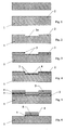
- FIG. 1 illustrates a sintered substrate 1 made of ZrO 2 , Al 2 O 3 or a mixture of both at the surface of which a layer 2 of a photosensitive polymer is deposited in order to form a layer formed for the selective deposition of the patterns .
- the thickness of this layer 2 depends on the variant used to form the patterns, depending on whether they will be substantially surface or raised.
- a mask is applied to this layer 2 of photosensitive polymer type RISTON® MM150, so as to selectively insolve this layer 2 under UV light to polymerize the portions of the layer 2 of photosensitive polymer that must remain on the substrate 1. It then develops this layer 2 in a 0.85% Na 2 CO 3 bath according to the indications of the supplier of the photosensitive polymer, to dissolve the non-insolated portions of the layer 2 to expose portions of surfaces 1a of the substrate 1. These portions present the shapes chosen for the formation of the patterns, as illustrated in FIG. 2. This procedure corresponds to a standard photolithographic process.
- the substrate 1 shown in section in FIGS. 7 actually corresponds to a portion of the ceramic element object of the present invention.
- This portion can correspond in particular to a radial section of this element ceramic consisting of a circular section ring rectangular.
- This ring preferably has a frustoconical shape, so that the visible surface 1a is inclined by relative to the axis of revolution of this ring.
- the mask used for training patterns in the polymer layer 2 is not a mask classic, but a polymer mask, thermoformed for him to give a shape complementary to that of the ceramic substrate.
- This polymeric mask that has a certain flexibility is applied on layer 2 with sufficient pressure for him to marry this layer 2 on all its surface.
- the substrate 1 is thus selectively coated by the layer 2, in a vacuum coating chamber, in which a first attachment layer 3 is deposited ( Figure 3) by the technique of physical deposition in phase vapor (PVD) and magnetron cathode sputtering makes it possible to ensure adhesion of the attachment layer 3, greater than that which would be obtained using the technique PVD without magnetron.
- the temperature of the substrate 1 can be kept low, well below 100 ° C during the operation deposit.
- the thickness of this second layer is greater than 100 nm, preferably between 500 nm and 15 ⁇ m.
- the parts were cleaned in an ultrasonic bath in a mixture of 20% isopropyl alcohol and 80% deionized water, for five minutes. Drying with a spray gun nitrogen.
- the substrates thus obtained are completely covered of the layer of titanium layer covered with the layer of gold, as shown in Figure 4.
- the substrate is subjected to 1 selectively coated with the polymer layer 2 and layers 3 and 4 (FIG. 4), to an electroforming operation, using the same noble metal as the one used for the second layer 4, in this example, gold.
- All the advantage of the invention lies in the power to keep the intact polymer mask for its use in the operation subsequent selective electroforming. So we drop by electroforming an additional layer 5 of desired thickness.
- the bath of gold used in this case is high in Au and allows electroforming of at least 0.10 mm, preferably some tenths of a millimeter thick.
- the operating conditions of the electroforming process are those indicated by the suppliers of the electroforming bath.
- the duration of the process depends on the thickness of the deposited layer.
- the growth rate of the deposit is about 10 ⁇ m / h.
- the polymer layer 2 is dissolved in so that there remains on the substrate 1 only the layers 3 and 4 which were on parts 1a where the substrate was ceramic was not covered by the polymer layer 2 dissolved. In this case, given the thickness of layers 3, 4, the patterns are practically on the surface of the substrate 1.
- the ceramic element, object of the present invention could be shaped polygonal frame with sloped face relative to the central axis of this element and constitute thus a pyramid trunk.
- FIG. 8 illustrates a ceramic ring 1, of shape frustoconical intended to be attached by elastic deformation on a telescope.
- This ring 1 is provided with relief patterns 5, according to the embodiment of FIG.
Landscapes
- Chemical & Material Sciences (AREA)
- Engineering & Computer Science (AREA)
- Ceramic Engineering (AREA)
- Materials Engineering (AREA)
- Structural Engineering (AREA)
- Organic Chemistry (AREA)
- Physical Vapour Deposition (AREA)
- Micromachines (AREA)
- Compositions Of Oxide Ceramics (AREA)
Abstract
Description
- une enceinte cylindrique en acier inoxydable avec système de pompage turbomoléculaire et pompe rotative à palettes;
- un porte-substrat de type carrousel à axe de rotation vertical et substrats positionnés verticalement. Possibilité de réaliser une pulvérisation cathodique RF polarisée sur le porte-substrat;
- deux cathodes magnétrons rectangulaires verticales montées face au carrousel selon un angle de 120° par rapport à l'axe du carrousel;
- deux cathodes:
- une cible Ti99,99
- une cible Au99,99
- une alimentation des cathodes par un générateur RF 13,56 MHz de 600 W avec une boíte d'accord d'impédance manuel;
- une alimentation en gaz (pureté: 5,7-6,0) par débitmètre de masse;
- un contrôle de pression par jauge Penning pour le contrôle du vide limite et par jauge capacitive (mesure absolue) pour le contrôle de la pression de travail.
- puissance RF sur porte-substrat:> 100 W
- flux d'argon:> 15 cm3/min
- flux d'oxygène:> 5 cm3/min
- pression totale:< 5 Pa
- durée: 20-30 min
- puissance RF sur la cathode:> 150 W
- flux d'argon:> 5 cm3/min
- pression d'argon:< 5 Pa
- l'épaisseur de la couche est >100 nm, de préférence >100 nm et <1500 nm
- puissance RF sur la cathode:> 50 W
- flux d'argon:> 10 cm3/min
- pression d'argon:< 5 Pa
- l'épaisseur de la couche est >100 nm, de préférence, >500 nm et <15 µm
Claims (10)
- Elément en céramique destiné à être rapporté sur une boíte de montre, dont la surface visible présente des motifs, caractérisé en ce que ces motifs sont fixés sur cette surface par une première couche d'accrochage (3) d'au moins 100 nm recouverte d'au moins uné seconde couche (4) du groupe Au, Ag, CrN, Ni, Pt, TiN, ZrN, Pd ou leurs alliages d'au moins 100 nm d'épaisseur.
- Elément en céramique selon la revendication 1, dont la forme est circulaire avec la face formant ladite surface visible de forme tronconique.
- Elément en céramique selon la revendication 1, dont la forme est celle d'un cadre polygonal avec la face formant ladite surface visible en forme de tronc de pyramide.
- Elément en céramique selon l'une des revendications précédentes, dans lequel ladite céramique est du ZrO2 de l'Al2O3 ou un mélange des deux.
- Elément en céramique selon l'une des revendications précédentes, dans lequel ladite première couche d'accrochage (3) est faite de Ti, Ta, Cr ou Th.
- Elément en céramique selon l'une des revendications précédentes, dans lequel, lesdits motifs sont formés par une couche supplémentaire (5) d'au moins 0,10 mm d'épaisseur, du même métal ou alliage que ladite seconde couche (4).
- Procédé de fabrication de l'élément en céramique selon l'une des revendications précédentes, caractérisé en ce que l'on dépose sélectivement sur ladite surface visible une couche soluble (2) dont l'épaisseur est au moins égale à la hauteur desdits motifs, on dépose sous vide sur ladite surface ainsi recouverte sélectivement une première couche d'accrochage (3) dé type Ti, Ta, Cr ou Th d'au moins 100 nm par dépôt physique en phase vapeur (PVD) avec pulvérisation cathodique magnétron suivie, sans mise à l'air, d'un dépôt PVD de ladite seconde couche (4) de Au, Pt, Ag, Cr, Pd, TiN, CrN, ZrN ou leurs alliages d'au moins 100 nm d'épaisseur et on dissout ladite couche soluble (2).
- Procédé selon la revendication 7 selon lequel, avant de dissoudre ladite couche soluble (2), on dépose une couche supplémentaire (5) d'un métal noble ou alliage de métaux nobles par électroformage.
- Procédé selon l'une des revendications 7 et 8, selon lequel on forme ladite couche soluble (2) en un polymère photosensible.
- Procédé selon les revendications 2 ou 3 et 9, selon lequel on applique sur ladite couche (2) de polymère photosensible un masque en polymère thermoplastique réalisé par thermoformage.
Priority Applications (7)
| Application Number | Priority Date | Filing Date | Title |
|---|---|---|---|
| EP03405924.6A EP1548525B2 (fr) | 2003-12-23 | 2003-12-23 | Elément en céramique pour boîte de montre et procédé de fabrication de cet élément |
| CNB2004100819067A CN100507765C (zh) | 2003-12-23 | 2004-12-16 | 制造用于表壳的陶瓷元件的方法及通过该方法获得的元件 |
| JP2004371658A JP2005181341A (ja) | 2003-12-23 | 2004-12-22 | 時計ケース用セラミック部材の製造方法及びその方法により得られる部材 |
| US11/061,289 US7628894B2 (en) | 2003-12-23 | 2005-02-18 | Process for manufacturing a ceramic element for a watch case and element obtained by this process |
| HK05105899.6A HK1073506B (en) | 2005-07-12 | Ceramic element for watch case and method of manufacturing the same | |
| US12/603,792 US8282270B2 (en) | 2003-12-23 | 2009-10-22 | Process for manufacturing a ceramic element for a watch case and element obtained by this process |
| JP2011138570A JP4921603B2 (ja) | 2003-12-23 | 2011-06-22 | 時計ケース用セラミック部材の製造方法及びその方法により得られる部材 |
Applications Claiming Priority (1)
| Application Number | Priority Date | Filing Date | Title |
|---|---|---|---|
| EP03405924.6A EP1548525B2 (fr) | 2003-12-23 | 2003-12-23 | Elément en céramique pour boîte de montre et procédé de fabrication de cet élément |
Publications (3)
| Publication Number | Publication Date |
|---|---|
| EP1548525A1 true EP1548525A1 (fr) | 2005-06-29 |
| EP1548525B1 EP1548525B1 (fr) | 2013-08-14 |
| EP1548525B2 EP1548525B2 (fr) | 2017-08-16 |
Family
ID=34530866
Family Applications (1)
| Application Number | Title | Priority Date | Filing Date |
|---|---|---|---|
| EP03405924.6A Expired - Lifetime EP1548525B2 (fr) | 2003-12-23 | 2003-12-23 | Elément en céramique pour boîte de montre et procédé de fabrication de cet élément |
Country Status (4)
| Country | Link |
|---|---|
| US (2) | US7628894B2 (fr) |
| EP (1) | EP1548525B2 (fr) |
| JP (2) | JP2005181341A (fr) |
| CN (1) | CN100507765C (fr) |
Cited By (3)
| Publication number | Priority date | Publication date | Assignee | Title |
|---|---|---|---|---|
| EP2730636A1 (fr) | 2012-11-07 | 2014-05-14 | Rolex S.A. | Matériau composite phosphorescent persistant |
| CN104160060A (zh) * | 2012-03-07 | 2014-11-19 | 山高刀具公司 | 具有金属基氮化物层的刀体和涂布该刀体的方法 |
| FR3077302A1 (fr) * | 2018-01-29 | 2019-08-02 | Avipo | Depot de pvd en fond de gravure |
Families Citing this family (13)
| Publication number | Priority date | Publication date | Assignee | Title |
|---|---|---|---|---|
| US7829793B2 (en) * | 2005-09-09 | 2010-11-09 | Magnecomp Corporation | Additive disk drive suspension manufacturing using tie layers for vias and product thereof |
| US8553364B1 (en) | 2005-09-09 | 2013-10-08 | Magnecomp Corporation | Low impedance, high bandwidth disk drive suspension circuit |
| US7781679B1 (en) * | 2005-09-09 | 2010-08-24 | Magnecomp Corporation | Disk drive suspension via formation using a tie layer and product |
| US8395866B1 (en) | 2005-09-09 | 2013-03-12 | Magnecomp Corporation | Resilient flying lead and terminus for disk drive suspension |
| CH714243B1 (fr) * | 2006-10-03 | 2019-04-15 | Swatch Group Res & Dev Ltd | Procédé d'électroformage et pièce ou couche obtenue par ce procédé. |
| CH710184B1 (fr) | 2007-09-21 | 2016-03-31 | Aliprandini Laboratoires G | Procédé d'obtention d'un dépôt d'alliage d'or jaune par galvanoplastie sans utilisation de métaux ou métalloïdes toxiques. |
| EP2312021B1 (fr) * | 2009-10-15 | 2020-03-18 | The Swatch Group Research and Development Ltd. | Procédé d'obtention d'un dépôt d'alliage d'or jaune par galvanoplastie sans utilisation de métaux toxiques |
| CN102912292B (zh) * | 2012-10-18 | 2014-05-28 | 东南大学 | 用于镍基合金紧固件表面的抗高温粘结涂层及其制备方法 |
| CN103572233B (zh) * | 2013-10-16 | 2015-09-23 | 中国科学院宁波材料技术与工程研究所 | 一种贵金属陶瓷薄膜及其制备方法 |
| CN105849064B (zh) | 2013-12-27 | 2019-05-31 | 东曹株式会社 | 氧化锆烧结体及其用途 |
| EP3034461B1 (fr) * | 2014-12-19 | 2020-07-01 | Rolex Sa | Fabrication d'un composant horloger multi-niveaux |
| CH714739A2 (fr) * | 2018-03-09 | 2019-09-13 | Swatch Group Res & Dev Ltd | Procédé de fabrication d’un décor métallique sur un cadran et cadran obtenu selon ce procédé. |
| EP3575447A1 (fr) * | 2018-05-28 | 2019-12-04 | The Swatch Group Research and Development Ltd | Procede de fabrication d'un decor metallique sur un cadran et cadran obtenu selon ce procede |
Citations (4)
| Publication number | Priority date | Publication date | Assignee | Title |
|---|---|---|---|---|
| JPS55135769A (en) * | 1979-04-11 | 1980-10-22 | Kawaguchiko Seimitsu Kk | Manufacture of dial for watch |
| EP0230853A1 (fr) * | 1986-01-20 | 1987-08-05 | W. Blösch AG | Procédé de fabrication d'une couche brasable d'un alliage sur un substrat céramique, de préférence céramique d'oxydes |
| EP0566820A1 (fr) * | 1992-04-21 | 1993-10-27 | W.C. Heraeus GmbH | Méthode pour la décoration des articles en silice avec des métaux précieux |
| US5358597A (en) * | 1991-09-04 | 1994-10-25 | Gte Laboratories Incorporated | Method of protecting aluminum nitride circuit substrates during electroless plating using sol-gel oxide films and article made therefrom |
Family Cites Families (39)
| Publication number | Priority date | Publication date | Assignee | Title |
|---|---|---|---|---|
| CH67374A4 (fr) * | 1974-01-18 | 1975-09-15 | ||
| DE2533524C3 (de) † | 1975-07-26 | 1978-05-18 | Licentia Patent-Verwaltungs-Gmbh, 6000 Frankfurt | Verfahren zur Herstellung eines Belages aus Kupfer oder einer Kupferlegierung auf einem Trägerkörper |
| DE2705225C2 (de) † | 1976-06-07 | 1983-03-24 | Nobuo Tokyo Nishida | Ornamentteil für Uhren usw. |
| US4213840A (en) † | 1978-11-13 | 1980-07-22 | Avantek, Inc. | Low-resistance, fine-line semiconductor device and the method for its manufacture |
| JPS55141569A (en) * | 1979-04-24 | 1980-11-05 | Kawaguchiko Seimitsu Kk | Manufacture of dial plate of watch |
| CH641313GA3 (fr) * | 1980-05-31 | 1984-02-29 | ||
| US4397566A (en) * | 1982-05-04 | 1983-08-09 | Montres Rado S.A. | Wrist-watch casing |
| US4512863A (en) * | 1983-09-09 | 1985-04-23 | Ppg Industries, Inc. | Stainless steel primer for sputtered films |
| JPS60141647A (ja) † | 1983-12-27 | 1985-07-26 | Seiko Instr & Electronics Ltd | カバ−ガラスの加飾方法 |
| US4565616A (en) * | 1984-04-30 | 1986-01-21 | Ppg Industries, Inc. | Method for producing a photoelectroforming mandrel |
| JPS644841Y2 (fr) † | 1985-03-19 | 1989-02-07 | ||
| FR2589484A1 (fr) † | 1985-11-04 | 1987-05-07 | Asulab Sa | Objet pourvu d'un revetement en metal precieux resistant a l'usure |
| CH667361GA3 (fr) * | 1986-02-04 | 1988-10-14 | ||
| US5100714A (en) * | 1986-07-24 | 1992-03-31 | Ceramic Packaging, Inc. | Metallized ceramic substrate and method therefor |
| US5058799A (en) * | 1986-07-24 | 1991-10-22 | Zsamboky Kalman F | Metallized ceramic substrate and method therefor |
| US4943486A (en) † | 1987-04-01 | 1990-07-24 | Seiko Epson Corporation | Coated article and method of production |
| US5082700A (en) * | 1987-08-10 | 1992-01-21 | Lanxide Technology Company, Lp | Method of making ceramic composite articles and articles made thereby |
| US4886766A (en) * | 1987-08-10 | 1989-12-12 | Lanxide Technology Company, Lp | Method of making ceramic composite articles and articles made thereby |
| JPH0192356A (ja) * | 1987-09-30 | 1989-04-11 | Pentel Kk | 装飾体およびその製造方法 |
| US5157258A (en) * | 1989-08-21 | 1992-10-20 | Rockwell International Corporation | Multicolor infrared focal plane arrays |
| WO1991014017A1 (fr) † | 1990-03-09 | 1991-09-19 | Kennametal Inc. | Deposition en phase gazeuse par procede physique de nitrure de titane sur un substrat non-conducteur |
| DE4009151A1 (de) * | 1990-03-22 | 1991-09-26 | Leybold Ag | Vorrichtung zum beschichten von substraten durch katodenzerstaeubung |
| JPH046263A (ja) † | 1990-04-24 | 1992-01-10 | Namiki Precision Jewel Co Ltd | サファイヤヘの貴金属加飾方法 |
| US5331608A (en) * | 1992-03-31 | 1994-07-19 | Citizen Watch Co., Ltd. | Electronic watch with an antenna for a receiving device |
| JPH0725199A (ja) † | 1993-07-12 | 1995-01-27 | Namiki Precision Jewel Co Ltd | サファイヤへの貴金属加飾方法 |
| CN1109126C (zh) † | 1993-12-28 | 2003-05-21 | 西铁城钟表有限公司 | 白色覆饰件及其生产方法 |
| EP0819995B1 (fr) * | 1995-04-07 | 1999-11-17 | Citizen Watch Co., Ltd. | Cadran de montre ou d'horloge a photopile |
| JPH09127261A (ja) * | 1995-11-01 | 1997-05-16 | Kawaguchiko Seimitsu Kk | 時計用文字板 |
| US5972233A (en) † | 1996-01-31 | 1999-10-26 | Refractal Design, Inc. | Method of manufacturing a decorative article |
| EP0844539B1 (fr) * | 1996-11-22 | 2003-11-19 | Montres Rado S.A. | Elément décoratif, notamment élément constitutif d'une pièce d'horlogerie |
| US6502982B1 (en) * | 1998-06-05 | 2003-01-07 | Montres Rado Sa | Structural component made of hard material for a wristwatch |
| JP3957920B2 (ja) * | 1998-06-11 | 2007-08-15 | キヤノン株式会社 | インクジェットヘッドの製造方法 |
| JP2001305244A (ja) † | 2000-04-20 | 2001-10-31 | Maruman Corporation:Kk | 電波腕時計のケース、同ケースの製造方法、並びに、同ケースを使用した電波腕時計 |
| TW517180B (en) * | 2001-02-23 | 2003-01-11 | Swatch Group Man Serv Ag | Timepiece with analogue display of time related information based on a decimal system |
| TW589167B (en) * | 2001-08-29 | 2004-06-01 | Rado Montres Sa | Link for watch bracelet |
| CN1212086C (zh) * | 2001-12-28 | 2005-07-27 | 西铁城时计株式会社 | 具有白色涂层膜的个人装饰品及其制造方法 |
| JP4072950B2 (ja) † | 2001-12-28 | 2008-04-09 | シチズンホールディングス株式会社 | 白色被膜を有する装飾品およびその製造方法 |
| JP2003268568A (ja) † | 2002-01-09 | 2003-09-25 | Citizen Watch Co Ltd | 白色被膜を有する装飾品およびその製造方法 |
| CH702127B1 (fr) † | 2007-05-25 | 2011-05-13 | Paul Hartzband | Pièce d'horlogerie munie d'un tour d'heures variable. |
-
2003
- 2003-12-23 EP EP03405924.6A patent/EP1548525B2/fr not_active Expired - Lifetime
-
2004
- 2004-12-16 CN CNB2004100819067A patent/CN100507765C/zh not_active Expired - Lifetime
- 2004-12-22 JP JP2004371658A patent/JP2005181341A/ja not_active Withdrawn
-
2005
- 2005-02-18 US US11/061,289 patent/US7628894B2/en not_active Expired - Lifetime
-
2009
- 2009-10-22 US US12/603,792 patent/US8282270B2/en not_active Expired - Lifetime
-
2011
- 2011-06-22 JP JP2011138570A patent/JP4921603B2/ja not_active Expired - Lifetime
Patent Citations (4)
| Publication number | Priority date | Publication date | Assignee | Title |
|---|---|---|---|---|
| JPS55135769A (en) * | 1979-04-11 | 1980-10-22 | Kawaguchiko Seimitsu Kk | Manufacture of dial for watch |
| EP0230853A1 (fr) * | 1986-01-20 | 1987-08-05 | W. Blösch AG | Procédé de fabrication d'une couche brasable d'un alliage sur un substrat céramique, de préférence céramique d'oxydes |
| US5358597A (en) * | 1991-09-04 | 1994-10-25 | Gte Laboratories Incorporated | Method of protecting aluminum nitride circuit substrates during electroless plating using sol-gel oxide films and article made therefrom |
| EP0566820A1 (fr) * | 1992-04-21 | 1993-10-27 | W.C. Heraeus GmbH | Méthode pour la décoration des articles en silice avec des métaux précieux |
Non-Patent Citations (1)
| Title |
|---|
| PATENT ABSTRACTS OF JAPAN vol. 0050, no. 05 (P - 044) 14 January 1981 (1981-01-14) * |
Cited By (3)
| Publication number | Priority date | Publication date | Assignee | Title |
|---|---|---|---|---|
| CN104160060A (zh) * | 2012-03-07 | 2014-11-19 | 山高刀具公司 | 具有金属基氮化物层的刀体和涂布该刀体的方法 |
| EP2730636A1 (fr) | 2012-11-07 | 2014-05-14 | Rolex S.A. | Matériau composite phosphorescent persistant |
| FR3077302A1 (fr) * | 2018-01-29 | 2019-08-02 | Avipo | Depot de pvd en fond de gravure |
Also Published As
| Publication number | Publication date |
|---|---|
| JP4921603B2 (ja) | 2012-04-25 |
| JP2011191321A (ja) | 2011-09-29 |
| CN1637662A (zh) | 2005-07-13 |
| HK1073506A1 (en) | 2005-10-07 |
| US7628894B2 (en) | 2009-12-08 |
| US20060011471A1 (en) | 2006-01-19 |
| JP2005181341A (ja) | 2005-07-07 |
| EP1548525B2 (fr) | 2017-08-16 |
| CN100507765C (zh) | 2009-07-01 |
| US8282270B2 (en) | 2012-10-09 |
| EP1548525B1 (fr) | 2013-08-14 |
| US20100110841A1 (en) | 2010-05-06 |
Similar Documents
| Publication | Publication Date | Title |
|---|---|---|
| EP1548524B1 (fr) | Elément en céramique pour boîte de montre et procédé de fabrication de cet élément | |
| EP1548525B2 (fr) | Elément en céramique pour boîte de montre et procédé de fabrication de cet élément | |
| EP3708384A1 (fr) | Element d'habillage ou cadran d'horlogerie ou de bijouterie en materiau conducteur | |
| EP3078436B1 (fr) | Procédé de fabrication d'un composant horloger | |
| CH713311A2 (fr) | Procédé de réalisation d'un motif sur une pièce horlogère et pièce horlogère. | |
| EP3220212A1 (fr) | Procédé de décoration d'un composant horloger | |
| EP1672436B1 (fr) | Cadran pour pièce d'horlogerie et procédés de fabrication de ce cadran | |
| EP0411079B1 (fr) | Procede de depot d'au moins une epaisseur d'au moins un materiau decoratif sur un objet et objet decoratif realise selon ce procede | |
| EP0627330B1 (fr) | Procédé d'obtention d'une empreinte gravée pourvue d'un matériau de contraste | |
| JP4909477B2 (ja) | 装飾部材及び装飾部材の製造方法 | |
| CH715191B1 (fr) | Procédé de décoration d'un composant d'habillage en horlogerie. | |
| KR101445371B1 (ko) | Pvd법을 이용한 금색 코팅막의 형성방법 및 이를 이용한 치과용 보철 | |
| CH716916A2 (fr) | Méthode de fabrication d'une surface décorative, objet décoratif à surface multicolore et montre comprenant de tels objets. | |
| HK1073506B (en) | Ceramic element for watch case and method of manufacturing the same | |
| CH712264A2 (fr) | Procédé de décoration d'un composant horloger. | |
| CH721342A2 (fr) | Procédé de décoration de composants horlogers | |
| HK40121608A (zh) | 导电材料制成的用於钟表或珠宝的外部元件或表盘 | |
| EP4206826A1 (fr) | Procédé de fabrication d'appliques sur un cadran | |
| CH721881A2 (fr) | Article avec un décor 3d revêtu et son procédé de fabrication | |
| HK1073507B (en) | Ceramic element for watch case and method of manufacturing the same | |
| JPH1172577A (ja) | 外装部材の製造方法及び電子機器 | |
| KR20020091336A (ko) | 희생층을 이용한 티타늄 콜리메이터 모재상에 증착된 티타늄계 오염층의 제거방법 |
Legal Events
| Date | Code | Title | Description |
|---|---|---|---|
| PUAI | Public reference made under article 153(3) epc to a published international application that has entered the european phase |
Free format text: ORIGINAL CODE: 0009012 |
|
| AK | Designated contracting states |
Kind code of ref document: A1 Designated state(s): AT BE BG CH CY CZ DE DK EE ES FI FR GB GR HU IE IT LI LU MC NL PT RO SE SI SK TR |
|
| AX | Request for extension of the european patent |
Extension state: AL LT LV MK |
|
| REG | Reference to a national code |
Ref country code: HK Ref legal event code: DE Ref document number: 1073506 Country of ref document: HK |
|
| 17P | Request for examination filed |
Effective date: 20050922 |
|
| AKX | Designation fees paid |
Designated state(s): CH DE FR GB LI |
|
| 17Q | First examination report despatched |
Effective date: 20070720 |
|
| GRAP | Despatch of communication of intention to grant a patent |
Free format text: ORIGINAL CODE: EPIDOSNIGR1 |
|
| GRAP | Despatch of communication of intention to grant a patent |
Free format text: ORIGINAL CODE: EPIDOSNIGR1 |
|
| GRAS | Grant fee paid |
Free format text: ORIGINAL CODE: EPIDOSNIGR3 |
|
| GRAA | (expected) grant |
Free format text: ORIGINAL CODE: 0009210 |
|
| AK | Designated contracting states |
Kind code of ref document: B1 Designated state(s): CH DE FR GB LI |
|
| REG | Reference to a national code |
Ref country code: GB Ref legal event code: FG4D Free format text: NOT ENGLISH |
|
| REG | Reference to a national code |
Ref country code: CH Ref legal event code: EP |
|
| REG | Reference to a national code |
Ref country code: CH Ref legal event code: NV Representative=s name: MOINAS AND SAVOYE SA, CH |
|
| REG | Reference to a national code |
Ref country code: DE Ref legal event code: R096 Ref document number: 60344711 Country of ref document: DE Effective date: 20131010 |
|
| REG | Reference to a national code |
Ref country code: HK Ref legal event code: GR Ref document number: 1073506 Country of ref document: HK |
|
| PLBI | Opposition filed |
Free format text: ORIGINAL CODE: 0009260 |
|
| 26 | Opposition filed |
Opponent name: G. ET F. CHATELAIN SA Effective date: 20140514 |
|
| PLAX | Notice of opposition and request to file observation + time limit sent |
Free format text: ORIGINAL CODE: EPIDOSNOBS2 |
|
| REG | Reference to a national code |
Ref country code: DE Ref legal event code: R026 Ref document number: 60344711 Country of ref document: DE Effective date: 20140514 |
|
| PLBB | Reply of patent proprietor to notice(s) of opposition received |
Free format text: ORIGINAL CODE: EPIDOSNOBS3 |
|
| REG | Reference to a national code |
Ref country code: FR Ref legal event code: PLFP Year of fee payment: 13 |
|
| REG | Reference to a national code |
Ref country code: CH Ref legal event code: PFA Owner name: ROLEX SA, CH Free format text: FORMER OWNER: ROLEX SA, CH |
|
| REG | Reference to a national code |
Ref country code: FR Ref legal event code: PLFP Year of fee payment: 14 |
|
| PUAH | Patent maintained in amended form |
Free format text: ORIGINAL CODE: 0009272 |
|
| STAA | Information on the status of an ep patent application or granted ep patent |
Free format text: STATUS: PATENT MAINTAINED AS AMENDED |
|
| 27A | Patent maintained in amended form |
Effective date: 20170816 |
|
| AK | Designated contracting states |
Kind code of ref document: B2 Designated state(s): CH DE FR GB LI |
|
| REG | Reference to a national code |
Ref country code: DE Ref legal event code: R102 Ref document number: 60344711 Country of ref document: DE |
|
| REG | Reference to a national code |
Ref country code: CH Ref legal event code: AELC |
|
| REG | Reference to a national code |
Ref country code: FR Ref legal event code: PLFP Year of fee payment: 15 |
|
| PGFP | Annual fee paid to national office [announced via postgrant information from national office to epo] |
Ref country code: GB Payment date: 20221219 Year of fee payment: 20 Ref country code: FR Payment date: 20221220 Year of fee payment: 20 Ref country code: DE Payment date: 20220624 Year of fee payment: 20 |
|
| PGFP | Annual fee paid to national office [announced via postgrant information from national office to epo] |
Ref country code: CH Payment date: 20221229 Year of fee payment: 20 |
|
| P01 | Opt-out of the competence of the unified patent court (upc) registered |
Effective date: 20230528 |
|
| REG | Reference to a national code |
Ref country code: DE Ref legal event code: R071 Ref document number: 60344711 Country of ref document: DE |
|
| REG | Reference to a national code |
Ref country code: CH Ref legal event code: PL |
|
| REG | Reference to a national code |
Ref country code: GB Ref legal event code: PE20 Expiry date: 20231222 |
|
| PG25 | Lapsed in a contracting state [announced via postgrant information from national office to epo] |
Ref country code: GB Free format text: LAPSE BECAUSE OF EXPIRATION OF PROTECTION Effective date: 20231222 |
|
| PG25 | Lapsed in a contracting state [announced via postgrant information from national office to epo] |
Ref country code: GB Free format text: LAPSE BECAUSE OF EXPIRATION OF PROTECTION Effective date: 20231222 |