EP1553731A2 - Système et contrôleur de communication de données - Google Patents
Système et contrôleur de communication de données Download PDFInfo
- Publication number
- EP1553731A2 EP1553731A2 EP05000139A EP05000139A EP1553731A2 EP 1553731 A2 EP1553731 A2 EP 1553731A2 EP 05000139 A EP05000139 A EP 05000139A EP 05000139 A EP05000139 A EP 05000139A EP 1553731 A2 EP1553731 A2 EP 1553731A2
- Authority
- EP
- European Patent Office
- Prior art keywords
- communication
- data
- master device
- driver
- communication system
- Prior art date
- Legal status (The legal status is an assumption and is not a legal conclusion. Google has not performed a legal analysis and makes no representation as to the accuracy of the status listed.)
- Withdrawn
Links
Images


Classifications
-
- G—PHYSICS
- G06—COMPUTING OR CALCULATING; COUNTING
- G06F—ELECTRIC DIGITAL DATA PROCESSING
- G06F13/00—Interconnection of, or transfer of information or other signals between, memories, input/output devices or central processing units
- G06F13/38—Information transfer, e.g. on bus
- G06F13/42—Bus transfer protocol, e.g. handshake; Synchronisation
- G06F13/4282—Bus transfer protocol, e.g. handshake; Synchronisation on a serial bus, e.g. I2C bus, SPI bus
- G06F13/4291—Bus transfer protocol, e.g. handshake; Synchronisation on a serial bus, e.g. I2C bus, SPI bus using a clocked protocol
-
- G—PHYSICS
- G06—COMPUTING OR CALCULATING; COUNTING
- G06F—ELECTRIC DIGITAL DATA PROCESSING
- G06F13/00—Interconnection of, or transfer of information or other signals between, memories, input/output devices or central processing units
- G06F13/10—Program control for peripheral devices
- G06F13/102—Program control for peripheral devices where the program performs an interfacing function, e.g. device driver
-
- G—PHYSICS
- G06—COMPUTING OR CALCULATING; COUNTING
- G06F—ELECTRIC DIGITAL DATA PROCESSING
- G06F9/00—Arrangements for program control, e.g. control units
- G06F9/06—Arrangements for program control, e.g. control units using stored programs, i.e. using an internal store of processing equipment to receive or retain programs
- G06F9/46—Multiprogramming arrangements
- G06F9/54—Interprogram communication
-
- H—ELECTRICITY
- H04—ELECTRIC COMMUNICATION TECHNIQUE
- H04L—TRANSMISSION OF DIGITAL INFORMATION, e.g. TELEGRAPHIC COMMUNICATION
- H04L12/00—Data switching networks
- H04L12/28—Data switching networks characterised by path configuration, e.g. LAN [Local Area Networks] or WAN [Wide Area Networks]
- H04L12/40—Bus networks
- H04L12/40006—Architecture of a communication node
- H04L12/40019—Details regarding a bus master
-
- H—ELECTRICITY
- H04—ELECTRIC COMMUNICATION TECHNIQUE
- H04L—TRANSMISSION OF DIGITAL INFORMATION, e.g. TELEGRAPHIC COMMUNICATION
- H04L12/00—Data switching networks
- H04L12/28—Data switching networks characterised by path configuration, e.g. LAN [Local Area Networks] or WAN [Wide Area Networks]
- H04L12/40—Bus networks
- H04L12/403—Bus networks with centralised control, e.g. polling
-
- H—ELECTRICITY
- H04—ELECTRIC COMMUNICATION TECHNIQUE
- H04L—TRANSMISSION OF DIGITAL INFORMATION, e.g. TELEGRAPHIC COMMUNICATION
- H04L12/00—Data switching networks
- H04L12/28—Data switching networks characterised by path configuration, e.g. LAN [Local Area Networks] or WAN [Wide Area Networks]
- H04L12/40—Bus networks
- H04L2012/40267—Bus for use in transportation systems
- H04L2012/40273—Bus for use in transportation systems the transportation system being a vehicle
Definitions
- the present invention relates to a data communication system which performs one-to-many data communications using a serial communication bus, specifically a serial peripheral interface (SPI) communication and an embedded controller equipped with such a data communication system.
- a serial communication bus specifically a serial peripheral interface (SPI) communication
- SPI serial peripheral interface
- One of well-known conventional arts for a data communication system is a technique to set physical protocol such as a baud rate and clock polarity phase in correspondence to a physical data communication means.
- SPI serial peripheral interface
- Another art is a technique using serial peripheral interface (hereinafter abbreviated as SPI) which is a clock synchronization serial bus communication having Chip Select signal lines as physical data communication means.
- SPI serial peripheral interface
- MPC555UMJ/AD R0.95" Pages 449 to 525)
- the embedded controller As one kind of embedded controller, for example, there has been a vehicle controller which controls a car engine, throttle, transmission, braking, steering, and battery on a car. Recently, the vehicle controllers have been requested to have higher functions to reduce fuel consumption and exhaust gas. For fine vehicle operation control, the embedded controller is equipped with an IC that processes signals of micro computers, sensors, and actuators. The results of measurement and output value data are transferred by data communication over an SPI communication bus.
- An object of this invention is to provide a data communication system which enables appropriate communications with a plurality of communication protocols on a single SPI communication bus.
- This invention is characterized by providing, as a serial communication driver, a communication driver for each device to set a physical protocol for each device on a serial communication bus and a communication manager to arbitrate serial communications on the bus.
- this invention provides a data communication system comprising a master device, a plurality of slave devices, a synchronous clock signal bus which connects the master device and the slave devices to transfer clock signals for synchronization of data transfer, at least one of a data transmission bus over which the master device sends data to the slave device in synchronism with a synchronous clock signal and a data reception bus over which the master device sends data from the slave device in synchronism with a synchronous clock signal, and Chip Select signal lines each of which connects the maser device to respective slave devices in the one-to-one manner for serial communications, wherein the data communication system is equipped with a serial communication driver containing device communication drivers each of which sets a physical protocol of each slave device and a communication manager which arbitrates serial communications between the master device and the slave devices.
- the serial communication driver should preferably have the characteristics below.
- the serial communication driver which consists of device communication drivers each of which sets a physical protocol of each slave device and a communication manager which arbitrates serial communications between the master device and the slave devices is executed for example by a program stored in ROM.
- This invention is applicable to all serial communication drivers independently of their names as far as they have above characteristics 1) to 3) even when the serial communication driver does not explicitly have device communication drivers and a communication manager.
- This invention is not limited to a serial communication driver having drivers and a manager by those names.
- the above means enables the simultaneous use of devices of different protocols on a single communication bus and serial communications at maximum transfer efficiencies by their protocols. As the result, the serial communication of the whole system is sped up.
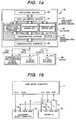
- FIG. 1(a) is an example of basic configuration of a data communication system in accordance with this invention.
- the data communication system 50 for SPI serial communications consists of a master device 51, slave devices (67, 71, and 75), at least either a data transmission bus which connects the master device 51 and the slave devices (67, 71, and 75) to transfer data from the master device 51 to the slave devices (67, 71, and 75) in synchronism with a synchronous clock signal or a data reception bus to transfer data from the slave devices (67, 71, and 75) to the master device 51, and Chip Select signal lines which respectively connect the master device 51 and each of the slave devices (67, 71, and 75) in the one-to-one manner to post implementation of communication.
- the data communication system 50 contains communication drivers (61a, 61b, and 61c) and a communication manager 61e which arbitrates serial communication between the master device 51 and the slave devices (67, 71, and 75).
- the communication manager 61e arbitrates serial communications to the slave devices (67, 71, and 75) via a communication interface 65 by their appropriate physical protocols.
- ECU electronice control unit
- FIG. 1(b) is an example of configuration of a data communication system which is a first embodiment of this invention.
- the data communication system of this embodiment consists of a main micro computer 1 (equivalent to the master device), a subsidiary micro computer 2A, and an I/O controlling driver IC 2B.
- the subsidiary micro computer 2A and the I/O controlling driver IC 2B are slave devices.
- the Chip Select signal line 3A is controlled by the main micro computer 1 to post implementation of a communication from the main micro computer 1 to the subsidiary micro computer 2A.
- the Chip Select signal line 3B is controlled by the main micro computer 1 to post implementation of a communication from the main micro computer 1 to the I/O controlling driver IC 2B.
- the clock signal bus 4 (equivalent to the synchronous clock signal bus) is controlled by the main micro computer 1 to output a clock signal to synchronize data transfer from the master device to the subsidiary device.
- the data transmission line 5 is controlled by the main micro computer 1 to output data from the main micro computer 1 to the subsidiary micro computer 2A or to the driver IC 2B in synchronism with a clock signal from the clock signal line 4.
- the data reception line 6 is controlled by the main micro computer 1 to output data from a slave device to the master device in synchronism with a clock signal.
- FIG. 2(a) is a first operation example of the data communication system of this embodiment, showing output signal waveforms of Chip Select signal lines (3A and 3B), clock signal line 4, data transmission line 5, and data reception line 6.
- the horizontal axis represents a time base and the vertical axis represents a signal voltage base.
- the Chip Select signal lines 3A and 3B are negated at a High voltage or asserted at a Low voltage.
- the synchronous clock signal 4 is negative in the High status or active in the Low status.
- the main micro computer 1 of FIG. 1(b) asserts the Chip Select signal line 3A to implement an SPI communication between the main micro computer 1 and the subsidiary micro computer 2A.
- the main micro computer 1 controls the clock signal line 4 to output clock signals by the size (e.g. 8 bits) of communication data at a baud rate (e.g. 2 MHz) fit for communication with the subsidiary micro computer.
- the main micro computer 1 outputs transmission data (TX DATA) 51 to the subsidiary micro computer 2 in synchronism with the clock signal.
- the subsidiary micro computer 2 outputs reception data (RX DATA) 61 to the main micro computer 1 in synchronism with the clock signal.
- the main micro computer 1 negates the Chip Select signal line 3A and ends the SPI communication between the main micro computer 1 and the subsidiary micro computer 2A.
- the main micro computer 1 asserts the Chip Select signal line 3B to implement an SPI communication between the main micro computer 1 and the I/O controlling driver IC 2B.
- the main micro computer 1 controls the clock signal line 4 to output clock signals by the size (e.g. 8 bits) of communication data at a baud rate (e.g. 1 MHz) fit for communication with the I/O controlling driver IC 2B.
- the main micro computer 1 outputs transmission data (TX DATA) 52 to the I/O controlling driver IC 2B in synchronism with the clock signal.
- the I/O controlling driver IC 2B outputs reception data (RX DATA) 62 to the main micro computer 1 in synchronism with the clock signal.
- the main micro computer 1 negates the Chip Select signal line 3B and ends the SPI communication between the main micro computer 1 and the I/O controlling driver IC 2B.
- frequencies of synchronous signals used in the SPI communication are one-to-one assigned to the Chip Select signal lines to be asserted. Therefore, for example, if devices in SPI communication interface have different upper clock frequency limits as in a combination of a high-performance micro computer and inexpensive driver ICs, synchronous clock frequencies fit for the slave devices can be used.
- the system configuration of FIG. 1(b) enables use of different protocols on the SPI communication bus.
- the data communication system of FIG. 1(b) connects a Chip Select signal lines 3, a clock signal line 4, a data transmission line 5, and a data reception line 6 to each slave device
- a data transmission line or a data reception line instead of both transmission and reception lines to a slave device.
- the sensor driver IC can be connected to a Chip Select signal line 3, a clock signal line 4, and a data reception line 6 to transfer data measured by sensors.
- FIG. 2(b) is a second operation example of the data communication system of this embodiment.
- the synchronous clock signal CLK43 is negative in the Low status or active in the High status while the Chip Select signal line 3A is asserted (during a time period T3).
- the synchronous clock signal 44 is negative in the Low status or active in the High status while the Chip Select signal line 3B is asserted (during a time period T4) or while the main micro computer 1 is communicating with the driver IC 2B.
- the numeric symbols 53, 54, 63, and 64 in FIG. 2(b) are respectively equivalent to the numeric symbols 51, 52, 61, and 62 in FIG. 2(a).
- the clock polarities 43, 44 of synchronous signals are one-to-one assigned to the Chip Select signal lines to be asserted. Therefore, the second operation example of FIG. 2(b) can have communication protocols of different clock polarity settings simultaneously on the SPI communication bus, for example a setting of making the synchronous clock signal active at a High voltage and a setting of making the synchronous clock signal active at a Low voltage.
- FIG. 3 shows a third operation example of the data communication system of this embodiment, showing signal waveforms for data communication.
- the Chip Select signal lines 3A and 3B are negated at a High voltage or asserted at a Low voltage. While the Chip Select signal line 3A is asserted (a time period of T5) or while the main micro computer 1 is communicating with a subsidiary micro computer 2A, the transmission data 55 and the reception data 65 are updated respectively by the main micro computer 1 and the subsidiary micro computer 2A at a rise of a clock signal (e.g. time t1) at which the synchronous clock signal 45 changes the status from negative to active.
- a clock signal e.g. time t1
- the transmission data 56 and the reception data 66 are updated respectively by the main micro computer 1 and the drive IC 2B at a fall of a clock signal (e.g. time t2) at which the synchronous clock signal 45 changes the status from active to negative.
- a clock signal e.g. time t2
- the third operation example of FIG. 3 can have communication protocols of different clock phase settings simultaneously on the SPI communication bus, for example a setting of updating data at a rise of the synchronous clock signal and a setting of updating data at a fall of the synchronous clock signal.
- FIG. 4 shows a vehicle in accordance of this embodiment.
- the vehicle 7 is equipped with an engine 8, an electronic control unit (ECU) 10 for controlling the engine, and an accelerator (gas pedal) 9 to be operated by a vehicle driver.
- the ECU 10 can be an embedded controller to control an automatic transmission, an electronic control throttle, and a motor-driven brake that are not shown in the drawing) in addition to controlling the engine.
- the ECU of FIG. 4 is an embedded controller to perform various kinds of vehicle-related control.
- FIG. 5 shows an example of ECU in accordance with the second embodiment of this invention.
- the ECU 10 is equipped with the data communication system of FIG. 1(b).
- the driver IC 2B receives values measured by sensors (e.g. accelerator opening) and sends them to the main micro computer 1 by the SPI communication.
- the main micro computer 1 receives the values, calculates output voltage values and port values from the measured values, and sends them to the driver IC 2B.
- the data communication between the main micro computer and subsidiary micro computers is also implemented by the SPI communication.
- FIG. 6 is an example of basic configuration of the main micro computer 1 of FIG. 5.
- the main micro computer 1 consists of memory 11, an SPI module 12 to control the SPI communication bus, a processor 13 to perform arithmetic operations, and a data bus 14, a direct memory access (DMA) controller 15.
- the SPI module 12 contains a control register 121 to set a physical protocol for SPI communication, transmission data memory 122 to store data to be sent out from the main micro computer and reception data memory 123 to store data that is received by the micro computer.
- DMA direct memory access
- Memory 11 contains application software 113 for computing control data and so on, communication middleware 112 for converting control data to data of the type and size available to the SPI driver, and an SPI driver 111 for controlling the SPI module to implement the SPI communication.
- the SPI driver 111 contains a communication protocol storage means 11121 for a subsidiary micro computer, a communication protocol storage means 11122 for a driver IC, and a communication control means 1111.
- Reference symbols 3A, 3B, and 4 to 6 of FIG. 6 are respectively equivalent to those of FIG. 1(b) and FIG. 5.
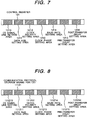
- FIG. 7 shows an example of configuration of the control register 121 in the SPI module.
- the control register 121 consists of a CS signal line setting area 1210 to set a Chip Select signal line to be asserted, a data size setting area 1211 to set the size (in bits) of data to be transferred, a clock polarity setting area 1212, a clock phase setting area 1213, a baud rate setting area 1214 to set a baud rate of a synchronous clock signal, a pre-transfer delay setting area 1215 to set a pre-transfer delay between assertion of a Chip Select signal line and output of a synchronous clock signal, and a post-transfer delay setting area 1216 to set a post-transfer delay between output of a synchronous clock signal and negation of a Chip Select signal line.
- FIG. 8 shows an example of configuration of the communication protocol storage means 11121 for a subsidiary micro computer in the SPI module.
- the communication protocol storage means 11121 for a subsidiary micro computer consists of a CS signal line storing area 111210 to store a Chip Select signal line to be asserted, a data size storing area 111211 to store the size (in bits) of data to be transferred, a clock polarity storing area 111212, a clock phase storing area 111213, a baud rate storing area 111214 to store a baud rate of a synchronous clock signal, a pre-transfer delay storing area 111215 to store a pre-transfer delay between assertion of a Chip Select signal line and output of a synchronous clock signal, and a post-transfer delay storing area 111216 to store a post-transfer delay between output of a synchronous clock signal and negation of a Chip Select signal line.
- FIG. 9 shows an operation flow chart of the communication control means 1111.
- the communication control means 1111 checks whether the system is now in communication or ready to start a communication. When finding the system is ready to start a communication, the communication control means 1111 goes to step S13.
- the communication control means 1111 sets transmission data in the transmission data memory 122. The processing at step S13 can be omitted when only data reception is implemented.
- the communication control means 1111 selects a communication protocol of a destination device from the communication protocol storage means 1112 and sets it in the control register 121.
- the communication control means 1111 submits a Start Communication command to the SPI module 12. The communication starts.
- the communication control means 1111 goes to step S16.
- the communication control means 1111 posts the Busy status to the communication middleware 112 and then temporarily stops communication processing.
- step S21 Control is transferred to step S21 when an End of Communication interrupt occurs at the end of the SPI communication that started at step S15.
- the post-processing of the SPI communication starts at step S21.
- the communication control means 1111 reads the received data from the reception data memory 123. The processing at step S22 can be omitted when only data transmission is implemented.
- the communication control means 1111 posts the Communication Processing Completed message to the communication middleware 112.
- communication processing is complete.
- the system configuration of FIG. 6 to FIG. 9 enables the use of different communication protocols simultaneously even when the SPI module has only one control register to set communication protocols for the SPI communication bus.
- FIG. 6 and FIG. 8 enables storage of a communication protocol specific to each destination device. Accordingly, even when a device connected to the communication bus is changed, the system has only to change its communication protocol storage means and can use the other communication protocol storage means without changing them. In other words, this enables efficient development of a data communication system that can use different communication protocols on a single SPI communication bus.
- FIG. 10 is an example of configuration of the communication control means of this embodiment.
- the communication control means 1111 consists of a communication control driver 11111 for a subsidiary micro computer, a communication control driver 11112 for a driver IC, and a communication control manager 11113.
- the communication control driver 11111 for a subsidiary micro computer contains a transmission buffer 111111 to store data to be transmitted and a reception buffer 111112 to store received data.
- the communication control driver 11112 for a driver IC contains a transmission buffer and a reception buffer.
- the communication control manager 11113 contains a communication job queue 111131 to store communication start requests.
- FIG. 11A and FIG. 11B respectively show examples of communication processing by the communication control means. This is explained with reference to FIG. 10. This example assumes that a request is made to communicate with the subsidiary micro computer 2.
- FIG. 11A shows a processing example in which the communication control driver 11111 is called by the communication middleware 112. As shown in FIG. 11A, the communication control driver 11111 is called by the communication middleware 112 at step S31 and starts communication processing. At step S32, the communication control driver 11111 checks whether the system is ready to communicate with a subsidiary micro computer (whether it is now communicating with the subsidiary micro computer). When finding the system is not ready for communication, the communication control driver 1111 goes to step S33. At step S33, the communication control driver 1111 posts the Busy status to the communication middleware 112 and ends processing.
- the communication control driver 1111 calls the communication control manager 11113.
- the communication control manager 11113 checks the content of the communication job queue 111131 for a job which is now running. When finding a running job, the communication control manager 11113 goes to step S35 and adds the requested destination (the subsidiary micro computer 2 in this example) to the end of jobs and stops the processing. When finding no running job, the communication control manager 11113 goes to step S36, registers the requested destination to the top of jobs, and calls a communication control driver for the destination (the communication control driver for the subsidiary micro computer in this example).
- the communication control driver for the subsidiary micro computer starts processing to implement the SPI communication. After the SPI communication starts, the communication control manager 11113 temporarily stops processing.
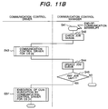
- FIG. 11B shows an operation flow chart in the case the communication control driver 11111 is called by an End of Communication interrupt from a processor.
- control is transferred to step S41 by the End of Communication interrupt from a processor and the post-processing of the SPI communication starts.
- the communication control manager checks the destination of a communication job which is in the top element of the job queue 111131.
- the communication control manager calls the communication end processing of a communication control driver (a communication control driver for the subsidiary micro computer in this example) for the destination set in the top job queue element.
- a communication control driver a communication control driver for the subsidiary micro computer in this example
- the communication control manager clears the communication job in the top job queue element and increments, by one, the number of respective communication jobs set in the job queue.
- the communication control manager checks the communication job queue 111131 for another communication job waiting to be implemented. When finding no communication job waiting to be implemented, the communication control manager ends processing. When finding a communication job to be implemented (a communication control driver for the driver IC in this example), the communication control manager calls step S37 to start communication with the communication control driver for a destination set in the top job queue element.
- FIG. 12 shows a communication starting flow of the communication control driver 11111 for a subsidiary micro computer as an example of communication start processing (step S37) of the communication control driver.
- the communication control driver 11111 sets transmission data by copying data from its transmission buffer 111111 onto transmission data memory 122 (of FIG. 6).
- the communication control driver 11111 sets a communication protocol for the subsidiary micro computer by copying the communication protocol from the communication protocol storage means 11121 (for the subsidiary micro computer) onto the control register 121.
- the communication control driver 11111 instructs the SPI module to start communication.
- FIG. 13 shows a communication ending flow of the communication control driver 11111 for a subsidiary micro computer as an example of communication end processing (step S43 of FIG. 11A) of the communication control driver.
- the communication control driver 11111 reads data (received by the SPI communication) from the reception data memory S123 and copies it onto the reception buffer 111112.
- the communication control driver 11111 posts the end of the SPI communication to the middleware 112.
- FIG. 14 is a conceptual drawing of operation of the data communication system in accordance with this embodiment.
- the (SPI) communication job queue (having elements 31 to 34) is empty.
- a request 21 is called to start communication with a subsidiary micro computer 2A.
- the communication request 21 is set in the top job queue element 31 as the job queue is empty.
- the communication protocol for the subsidiary micro computer is set and the SPI communication 22 starts.
- another request 23 is called to start communication with a driver IC 2B.
- the communication request 23 is set in the next job queue element 32 as the top job queue element 31 is already occupied.
- the main micro computer temporarily stops the processing and waits for start of communication 24.
- the communication with the subsidiary micro computer 2A is complete.
- the main micro computer checks the communication job queue, implements post-processing of communication of the subsidiary micro computer 2A which is set in the top job queue element, and updates the content of the job queue. Then, the main micro computer checks the job queue and implements a communication 25 with a driver IC (which is now in job queue element 31 by updating and shifting from queue element 32 to queue element 31).
- the communication with the driver IC 2B is complete.
- the main micro computer checks the communication job queue, implements post-processing of communication of the driver IC 2B which is set in the top job queue element 31, and updates the content of the job queue. Then, the main micro computer checks the job queue again. When finding the job queue is empty, the main micro computer ends the SPI communication processing.
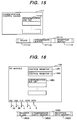
- FIG. 15 shows another configuration example of the communication control means 1111 in the data communication system in accordance with this embodiment.
- the communication control means 1111 contains a communication job list 11114.
- Each element of the communication job list 11114 stores information of a destination device 111141, transmission buffer 111142, and reception buffer 111143.
- the communication middleware sets transmission data and destination data in the communication job list and requests to start the SPI communication.
- the processor reads the registered communication jobs from the communication job list and implements the jobs in sequence.
- the received data can be read from the reception buffer.
- the DMA controller 15 when used, can execute communication jobs (copying from the transmission buffer to data memory 122, copying from the communication protocol storage means 1112 to the control register, and copying from reception data memory 123 to the reception buffer 111143) without imposing a burden on the processor 13.
- FIG. 16 shows another configuration example of the SPI module 12 in the data communication system in accordance with this embodiment.
- the reference symbols 3A, 3B, and 4 to 6 are respectively equivalent to those of FIG. 1(b) and FIG. 5.
- the SPI module 12B contains some control registers (12B1 and 12B2) and a communication job list 12B3. Each control register has the same configuration as the control register 121 of FIG. 7.
- Each element of the communication job list 12B3 stores information 12B31 of a control register to be used, transmission data memory 12B32 to store data to be transmitted, and reception data memory 12B33 to store received data.
- the SPI driver 111 sets transmission data and a required control register in the communication job list 12B3 and requests to start the SPI communication.
- the SPI module 12B reads the registered communication jobs from the communication job list 12B3 and implements the jobs in sequence. When all communication jobs are completed, the received data can be read from the reception data memory 12B33. As explained in the above configuration example, it is possible to provide two or more control registers and physically switch communication protocols.
- step S13 of FIG. 9A data to be transmitted is stored in the transmission data memory 122.
- the step S13 can be omitted when only data reception is implemented.
- a communication protocol for the destination device is set in the control register 121 in reference to the communication protocol storage means 1112.
- the communication control means submits a command to start the SPI communication to the SPI module 12 and then temporarily stops communication processing.
- control is transferred to step S16.
- the data communication system in accordance with each of the above embodiments of this invention switches the baud rate of a synchronous clock signal by the asserted Chip Select signal line in serial communications such as SPI communication. Therefore, the data communication system can communicate using a communication protocol optimum to a destination device.
- the data communication system switches the clock polarity of a synchronous clock signal by the asserted Chip Select signal line in SPI communication. Therefore, the data communication system can communicate using a communication protocol optimum to a destination device. Further, the data communication system switches the clock phase of a synchronous clock signal by the asserted Chip Select signal line in SPI communication. Therefore, the data communication system can communicate using a communication protocol optimum to a destination device.
- the data communication system is equipped with a communication protocol storage means for each destination slave device and a communication control means which calls a proper communication protocol storage means to implement an SPI communication. Therefore, the data communication system can communicate using a communication protocol optimum to a destination device.
- the data communication system is equipped with a communication control driver for each destination slave device and a communication control manager which exclusively controls a communication control driver. Therefore, the data communication system can communicate using a communication protocol optimum to a destination device.
- the communication protocol storage means and communication control means are accomplished by software that runs on memory, even an SPI module having only one control register can switch communication protocols. Therefore, the data communication system can communicate using a communication protocol optimum to a destination device.
- the SPI module having only one control register can switch communication protocols quickly.
Landscapes
- Engineering & Computer Science (AREA)
- Theoretical Computer Science (AREA)
- Physics & Mathematics (AREA)
- General Engineering & Computer Science (AREA)
- General Physics & Mathematics (AREA)
- Software Systems (AREA)
- Computer Networks & Wireless Communication (AREA)
- Signal Processing (AREA)
- Communication Control (AREA)
- Information Transfer Systems (AREA)
- Small-Scale Networks (AREA)
Applications Claiming Priority (2)
| Application Number | Priority Date | Filing Date | Title |
|---|---|---|---|
| JP2004002284A JP4834294B2 (ja) | 2004-01-07 | 2004-01-07 | データ通信装置及びそれを用いたコントローラ |
| JP2004002284 | 2004-01-07 |
Publications (2)
| Publication Number | Publication Date |
|---|---|
| EP1553731A2 true EP1553731A2 (fr) | 2005-07-13 |
| EP1553731A3 EP1553731A3 (fr) | 2007-09-05 |
Family
ID=34587688
Family Applications (1)
| Application Number | Title | Priority Date | Filing Date |
|---|---|---|---|
| EP05000139A Withdrawn EP1553731A3 (fr) | 2004-01-07 | 2005-01-05 | Système et contrôleur de communication de données |
Country Status (4)
| Country | Link |
|---|---|
| US (1) | US7228372B2 (fr) |
| EP (1) | EP1553731A3 (fr) |
| JP (1) | JP4834294B2 (fr) |
| CN (1) | CN1637256A (fr) |
Cited By (7)
| Publication number | Priority date | Publication date | Assignee | Title |
|---|---|---|---|---|
| EP1950399A1 (fr) * | 2007-01-24 | 2008-07-30 | Siemens Aktiengesellschaft | Système doté de déviations dýutilisateurs |
| EP1926023A3 (fr) * | 2006-11-27 | 2008-10-22 | Denso Corporation | Système de communications et unité de commande électronique comprenant le système de communication pour la commande de véhicule |
| WO2013092101A1 (fr) * | 2011-12-21 | 2013-06-27 | Endress+Hauser Gmbh+Co. Kg | Dispositif de transmission de données synchrone |
| FR2987528A1 (fr) * | 2012-02-28 | 2013-08-30 | Valeo Sys Controle Moteur Sas | Procede de communication periodique entre au moins un premier systeme et au moins un deuxieme systeme par l'intermediaire d'une liaison serie synchrone full duplex |
| EP3174252A1 (fr) | 2015-11-26 | 2017-05-31 | Gemalto Sa | Système de communication |
| WO2017099959A1 (fr) * | 2015-12-10 | 2017-06-15 | Qualcomm Incorporated | Interface périphérique série améliorée à commande de flux matériel |
| CN107885690A (zh) * | 2017-10-13 | 2018-04-06 | 上海剑桥科技股份有限公司 | Spi交换系统及其控制方法 |
Families Citing this family (43)
| Publication number | Priority date | Publication date | Assignee | Title |
|---|---|---|---|---|
| JP4834294B2 (ja) * | 2004-01-07 | 2011-12-14 | 日立オートモティブシステムズ株式会社 | データ通信装置及びそれを用いたコントローラ |
| EP1764803A1 (fr) * | 2005-09-09 | 2007-03-21 | STMicroelectronics S.r.l. | Architecture de mémoire avec interface périphérique sérielle |
| WO2007116487A1 (fr) * | 2006-03-31 | 2007-10-18 | Fujitsu Limited | Dispositif mémoire, procédé de support de prise en charge de corrections d'erreur, programme de prise en charge, carte mémoire, carte de circuits imprimés et dispositif électronique |
| CN101401077A (zh) | 2006-03-31 | 2009-04-01 | 富士通株式会社 | 存储装置及其控制方法和其控制程序、存储卡、电路基板及电子设备 |
| JPWO2007116486A1 (ja) | 2006-03-31 | 2009-08-20 | 富士通株式会社 | メモリ装置、その制御方法、その制御プログラム、メモリ・カード、回路基板及び電子機器 |
| US7958291B2 (en) * | 2006-10-10 | 2011-06-07 | Atmel Rousset S.A.S. | Supplemental communication interface |
| WO2008089685A1 (fr) * | 2007-01-21 | 2008-07-31 | Print-Rite Technology Development Co., Ltd Of Zhuhai | Appareil de communication, système de communication série en synchronisation et procédé correspondant |
| JP4415027B2 (ja) * | 2007-03-12 | 2010-02-17 | マーン・ベー・オグ・ドバルドヴェー・ディーゼール・アクティーゼルスカブ | 多気筒内燃機関用の制御方法及びシステム |
| US7845568B2 (en) * | 2007-05-09 | 2010-12-07 | Atmel Rousset S.A.S. | Managing power and timing in a smart card device |
| CN101399654B (zh) * | 2007-09-25 | 2011-08-03 | 华为技术有限公司 | 一种串行通信方法和装置 |
| US8060681B2 (en) * | 2007-11-27 | 2011-11-15 | Microsoft Corporation | Interface protocol and API for a wireless transceiver |
| DE102008005959B4 (de) * | 2008-01-24 | 2009-09-10 | Continental Automotive Gmbh | Motorsteuereinheit und Motorsteuerverfahren für eine Brennkraftmaschine |
| DE102008039564B4 (de) * | 2008-08-25 | 2018-06-21 | Continental Automotive Gmbh | Verfahren zum Abarbeiten von Aufgaben und System mit einem ersten und einem zweiten Steuergerät |
| DE102009027625A1 (de) * | 2009-07-10 | 2011-01-13 | Robert Bosch Gmbh | Elektrische Schaltung zur Übertragung von Signalen zwischen zwei Mastern und einem oder mehreren Slaves |
| CN102023942B (zh) * | 2009-09-09 | 2012-10-10 | 鸿富锦精密工业(深圳)有限公司 | Spi外设访问装置及方法 |
| US8176209B2 (en) | 2009-11-05 | 2012-05-08 | Electronics And Telecommunications Research Institute | Data communication system |
| JP2012113571A (ja) * | 2010-11-25 | 2012-06-14 | Brother Ind Ltd | 情報収集システム |
| US8832344B2 (en) | 2011-03-30 | 2014-09-09 | Kilseong Ha | Baseboard, extension module, and structure for connecting baseboard and extension module |
| TWI547784B (zh) * | 2011-04-22 | 2016-09-01 | 緯創資通股份有限公司 | 動態調整匯流排時脈的方法及其裝置 |
| JP2012247907A (ja) * | 2011-05-26 | 2012-12-13 | Toyota Motor Corp | 情報処理装置 |
| CN102193889B (zh) * | 2011-06-08 | 2014-01-22 | 杭州国芯科技股份有限公司 | 一种i2c总线转发器及其读写方法 |
| US8966355B2 (en) * | 2012-02-15 | 2015-02-24 | Infineon Technologies Ag | Apparatus and method for comparing pairs of binary words |
| US8984196B2 (en) * | 2012-04-12 | 2015-03-17 | Lenovo Enterprise Solutions (Singapore) Ptd. Ltd. | Accessing peripheral devices |
| US9230290B2 (en) | 2012-04-27 | 2016-01-05 | Hewlett Packard Enterprise Development Lp | Power meter consumption system and method to verify data stored in a register by comparing an address of the register with request for data of the register |
| WO2013185293A1 (fr) * | 2012-06-12 | 2013-12-19 | 深圳市摩西尔电子有限公司 | Mémoire de bus série, et système et procédé de transmission de bus série |
| US9214232B2 (en) | 2012-07-26 | 2015-12-15 | Micron Technology, Inc. | Methods and apparatuses for calibrating data sampling points |
| CN104133792B (zh) * | 2013-05-03 | 2017-02-15 | 珠海全志科技股份有限公司 | 精简串行总线通信方法及系统 |
| US9292409B2 (en) * | 2013-06-03 | 2016-03-22 | Infineon Technologies Ag | Sensor interfaces |
| US9772970B2 (en) * | 2013-08-29 | 2017-09-26 | Atmel Corporation | Multi-protocol serial communication interface |
| CN103616836A (zh) * | 2013-11-28 | 2014-03-05 | 盛瑞传动股份有限公司 | 一种自动变速器用存储芯片 |
| JP6349783B2 (ja) * | 2014-02-28 | 2018-07-04 | 富士通株式会社 | 端末装置、サーバ装置、デバイスドライバプログラム及び外部周辺機器制御方法 |
| KR101565584B1 (ko) * | 2014-04-07 | 2015-11-04 | (주)에프씨아이 | Spi 통신 기반의 데이터 전송 장치 및 방법 |
| PL3001323T3 (pl) * | 2014-09-26 | 2018-01-31 | Oberthur Technologies | Szeregowy interfejs urządzeń peryferyjnych |
| WO2016203356A1 (fr) * | 2015-06-16 | 2016-12-22 | Theranica Bio-Electronics Ltd. | Détection multiple utilisant de multiples protocoles en série sur un schéma d'interconnexion commun |
| KR101815961B1 (ko) * | 2015-12-15 | 2018-01-08 | 현대오트론 주식회사 | Spi 인터페이스 장치 및 이를 이용한 통신 방법 |
| CN107562666B (zh) * | 2017-09-26 | 2020-10-23 | 威创集团股份有限公司 | 基于spi总线的设备间通信的方法、系统及相关装置 |
| JP6764387B2 (ja) * | 2017-09-28 | 2020-09-30 | 富士通フロンテック株式会社 | 複数スキャナ制御プログラム、pos端末、複数スキャナ制御方法 |
| JP6933183B2 (ja) * | 2018-03-30 | 2021-09-08 | オムロン株式会社 | セーフティ制御システムおよびセーフティ制御ユニット |
| CN110782828B (zh) * | 2018-07-26 | 2021-05-11 | 深圳市爱协生科技有限公司 | 显示装置 |
| JP7327029B2 (ja) | 2019-09-19 | 2023-08-16 | 京セラドキュメントソリューションズ株式会社 | 画像形成装置、データ通信方法 |
| CN112882400B (zh) * | 2021-01-12 | 2022-10-25 | 杭州芯格微电子有限公司 | 同时驱动多个i2c从设备的方法及由控制器同时驱动的芯片 |
| CN112506838A (zh) * | 2021-02-03 | 2021-03-16 | 青岛鼎信通讯股份有限公司 | 一种应用于ir46电表检定装置的spi时钟同步方法 |
| JP7393380B2 (ja) | 2021-04-21 | 2023-12-06 | 矢崎総業株式会社 | 通信システム及び通信システムの配置方法 |
Citations (2)
| Publication number | Priority date | Publication date | Assignee | Title |
|---|---|---|---|---|
| US6038400A (en) | 1995-09-27 | 2000-03-14 | Linear Technology Corporation | Self-configuring interface circuitry, including circuitry for identifying a protocol used to send signals to the interface circuitry, and circuitry for receiving the signals using the identified protocol |
| US20020188782A1 (en) | 2001-06-08 | 2002-12-12 | Victor Fay | Generic serial bus architecture |
Family Cites Families (12)
| Publication number | Priority date | Publication date | Assignee | Title |
|---|---|---|---|---|
| US2000A (en) * | 1841-03-12 | Improvement in the manufacture of starch | ||
| US4855905A (en) * | 1987-04-29 | 1989-08-08 | International Business Machines Corporation | Multiprotocol I/O communications controller unit including emulated I/O controllers and tables translation of common commands and device addresses |
| GB2264845B (en) * | 1992-02-28 | 1995-09-20 | Texas Instruments Ltd | Local area network adaptive circuit for multiple network types |
| GB2264844B (en) * | 1992-02-28 | 1995-09-20 | Texas Instruments Ltd | Signal interface for coupling a network front end circuit to a network adapter circuit |
| US5579299A (en) * | 1994-12-16 | 1996-11-26 | Chrysler Corporation | Communications network, a dual mode data transfer system therefor |
| US6163538A (en) * | 1997-10-09 | 2000-12-19 | Monarch Marketing Systems, Inc. | Wireless serial port transceiver |
| US6691183B1 (en) * | 1998-05-20 | 2004-02-10 | Invensys Systems, Inc. | Second transfer logic causing a first transfer logic to check a data ready bit prior to each of multibit transfer of a continous transfer operation |
| JP3692820B2 (ja) | 1999-03-10 | 2005-09-07 | 株式会社デンソー | 自動車用制御装置 |
| US6611860B1 (en) * | 1999-11-17 | 2003-08-26 | I/O Controls Corporation | Control network with matrix architecture |
| US6523081B1 (en) * | 1999-11-22 | 2003-02-18 | Texas Instruments Incorporated | Architecture using dedicated endpoints and protocol for creating a multi-application interface and improving bandwidth over universal serial bus |
| JP4658374B2 (ja) * | 2001-05-10 | 2011-03-23 | 株式会社リコー | 無線通信方法及びそのマスター端末 |
| JP4834294B2 (ja) * | 2004-01-07 | 2011-12-14 | 日立オートモティブシステムズ株式会社 | データ通信装置及びそれを用いたコントローラ |
-
2004
- 2004-01-07 JP JP2004002284A patent/JP4834294B2/ja not_active Expired - Lifetime
- 2004-12-21 US US11/016,769 patent/US7228372B2/en not_active Expired - Lifetime
- 2004-12-30 CN CN200410081836.5A patent/CN1637256A/zh active Pending
-
2005
- 2005-01-05 EP EP05000139A patent/EP1553731A3/fr not_active Withdrawn
Patent Citations (2)
| Publication number | Priority date | Publication date | Assignee | Title |
|---|---|---|---|---|
| US6038400A (en) | 1995-09-27 | 2000-03-14 | Linear Technology Corporation | Self-configuring interface circuitry, including circuitry for identifying a protocol used to send signals to the interface circuitry, and circuitry for receiving the signals using the identified protocol |
| US20020188782A1 (en) | 2001-06-08 | 2002-12-12 | Victor Fay | Generic serial bus architecture |
Cited By (15)
| Publication number | Priority date | Publication date | Assignee | Title |
|---|---|---|---|---|
| EP1926023A3 (fr) * | 2006-11-27 | 2008-10-22 | Denso Corporation | Système de communications et unité de commande électronique comprenant le système de communication pour la commande de véhicule |
| US7848856B2 (en) | 2006-11-27 | 2010-12-07 | Denso Corporation | Communication system and electronic control unit including communication system for vehicle control |
| EP1950399A1 (fr) * | 2007-01-24 | 2008-07-30 | Siemens Aktiengesellschaft | Système doté de déviations dýutilisateurs |
| WO2013092101A1 (fr) * | 2011-12-21 | 2013-06-27 | Endress+Hauser Gmbh+Co. Kg | Dispositif de transmission de données synchrone |
| US9100142B2 (en) | 2011-12-21 | 2015-08-04 | Endress + Hauser Gmbh + Co. Kg | Synchronous data transmission system |
| KR20140130726A (ko) * | 2012-02-28 | 2014-11-11 | 발레오 시스템므 드 꽁트롤르 모뙤르 | 전이중 동기 직렬 링크를 통해 적어도 하나의 제1 시스템과 적어도 하나의 제2 시스템 간의 주기적 통신 방법 |
| WO2013128112A1 (fr) * | 2012-02-28 | 2013-09-06 | Valeo Systemes De Controle Moteur | Procede de communication periodique entre au moins un premier systeme et au moins un deuxieme systeme par l'intermediaire d'une liaison serie synchrone full duplex |
| FR2987528A1 (fr) * | 2012-02-28 | 2013-08-30 | Valeo Sys Controle Moteur Sas | Procede de communication periodique entre au moins un premier systeme et au moins un deuxieme systeme par l'intermediaire d'une liaison serie synchrone full duplex |
| US9584301B2 (en) | 2012-02-28 | 2017-02-28 | Valeo Systemes De Controle Moteur | Periodic communication method between at least one first system and at least one second system by means of a full-duplex synchronous serial link |
| KR102000326B1 (ko) | 2012-02-28 | 2019-09-27 | 발레오 시스템므 드 꽁트롤르 모뙤르 | 전이중 동기 직렬 링크를 통해 적어도 하나의 제1 시스템과 적어도 하나의 제2 시스템 간의 주기적 통신 방법 |
| EP3174252A1 (fr) | 2015-11-26 | 2017-05-31 | Gemalto Sa | Système de communication |
| WO2017089543A1 (fr) | 2015-11-26 | 2017-06-01 | Gemalto Sa | Système de communication |
| WO2017099959A1 (fr) * | 2015-12-10 | 2017-06-15 | Qualcomm Incorporated | Interface périphérique série améliorée à commande de flux matériel |
| US10140243B2 (en) | 2015-12-10 | 2018-11-27 | Qualcomm Incorporated | Enhanced serial peripheral interface with hardware flow-control |
| CN107885690A (zh) * | 2017-10-13 | 2018-04-06 | 上海剑桥科技股份有限公司 | Spi交换系统及其控制方法 |
Also Published As
| Publication number | Publication date |
|---|---|
| EP1553731A3 (fr) | 2007-09-05 |
| CN1637256A (zh) | 2005-07-13 |
| US20050172059A1 (en) | 2005-08-04 |
| JP2005196486A (ja) | 2005-07-21 |
| US7228372B2 (en) | 2007-06-05 |
| JP4834294B2 (ja) | 2011-12-14 |
Similar Documents
| Publication | Publication Date | Title |
|---|---|---|
| US7228372B2 (en) | Data communication system with an SPI bus having a plurality of devices wherein data communications are enabled using communication protocols optimum to respective devices | |
| US5420985A (en) | Bus arbiter system and method utilizing hardware and software which is capable of operation in distributed mode or central mode | |
| JPH0534699B2 (fr) | ||
| WO2012088293A2 (fr) | Interface de moteur de protocole commune pour une interface de dispositif de commande | |
| EP1063594B1 (fr) | Un gestionnaire d'interruption et un micro-ordinateur comprenant ce gestionnaire | |
| EP1187028B1 (fr) | Autorisation immédiate de demandes dans un arbitre de bus d'un système de bus | |
| JP2012034375A (ja) | データ通信装置及びそれを用いたコントローラ | |
| Bhakthavatchalu | Design and Implementation of MIPI I3C master controller SubSystems | |
| JP2004220326A (ja) | 制御ソフトウエア構造およびこの構造を用いた制御装置 | |
| JPH1185668A (ja) | バス制御装置 | |
| EP1879113B1 (fr) | Équipement de contrôle avec appareil de communication | |
| KR100633742B1 (ko) | 주변 장치로부터 데이터 전송 크기를 자동으로 갱신하는직접 메모리 액세스 제어 장치 및 방법 | |
| CN1969268B (zh) | 主机控制器、总线通信设备和操作主机控制器的方法 | |
| US20040093439A1 (en) | Data processing control apparatus and DMA controller | |
| JP4828947B2 (ja) | 車両制御装置の入出力装置 | |
| WO2004107188A1 (fr) | Processeur de donnees et procede de communication de donnees | |
| CN115422100A (zh) | 直接内存存取控制装置、数据传输方法和数据传输系统 | |
| JPH05134980A (ja) | バスシステム | |
| JPS60136853A (ja) | デ−タ転送方式 | |
| JP2003099390A (ja) | Dma回路 | |
| JPH0199154A (ja) | データ転送装置 | |
| JPS63271537A (ja) | 割り込み制御装置 | |
| JPH1141297A (ja) | プログラマブルシーケンサーを使用したdmaコントローラ | |
| JPH1196109A (ja) | バスマスタ接続装置 | |
| JPH0314021A (ja) | プリンタ |
Legal Events
| Date | Code | Title | Description |
|---|---|---|---|
| PUAI | Public reference made under article 153(3) epc to a published international application that has entered the european phase |
Free format text: ORIGINAL CODE: 0009012 |
|
| AK | Designated contracting states |
Kind code of ref document: A2 Designated state(s): AT BE BG CH CY CZ DE DK EE ES FI FR GB GR HU IE IS IT LI LT LU MC NL PL PT RO SE SI SK TR |
|
| AX | Request for extension of the european patent |
Extension state: AL BA HR LV MK YU |
|
| PUAL | Search report despatched |
Free format text: ORIGINAL CODE: 0009013 |
|
| AK | Designated contracting states |
Kind code of ref document: A3 Designated state(s): AT BE BG CH CY CZ DE DK EE ES FI FR GB GR HU IE IS IT LI LT LU MC NL PL PT RO SE SI SK TR |
|
| AX | Request for extension of the european patent |
Extension state: AL BA HR LV MK YU |
|
| RIC1 | Information provided on ipc code assigned before grant |
Ipc: H04L 12/40 20060101ALI20070727BHEP Ipc: G06F 13/42 20060101AFI20070727BHEP |
|
| 17P | Request for examination filed |
Effective date: 20080305 |
|
| AKX | Designation fees paid |
Designated state(s): DE |
|
| 17Q | First examination report despatched |
Effective date: 20080912 |
|
| STAA | Information on the status of an ep patent application or granted ep patent |
Free format text: STATUS: THE APPLICATION IS DEEMED TO BE WITHDRAWN |
|
| 18D | Application deemed to be withdrawn |
Effective date: 20160802 |