EP1556888B1 - Verfahren zur herstellung von abtrennbaren substraten - Google Patents
Verfahren zur herstellung von abtrennbaren substraten Download PDFInfo
- Publication number
- EP1556888B1 EP1556888B1 EP03809826A EP03809826A EP1556888B1 EP 1556888 B1 EP1556888 B1 EP 1556888B1 EP 03809826 A EP03809826 A EP 03809826A EP 03809826 A EP03809826 A EP 03809826A EP 1556888 B1 EP1556888 B1 EP 1556888B1
- Authority
- EP
- European Patent Office
- Prior art keywords
- ions
- layer
- roughness
- process according
- previous
- Prior art date
- Legal status (The legal status is an assumption and is not a legal conclusion. Google has not performed a legal analysis and makes no representation as to the accuracy of the status listed.)
- Expired - Lifetime
Links
Images
Classifications
-
- H—ELECTRICITY
- H10—SEMICONDUCTOR DEVICES; ELECTRIC SOLID-STATE DEVICES NOT OTHERWISE PROVIDED FOR
- H10P—GENERIC PROCESSES OR APPARATUS FOR THE MANUFACTURE OR TREATMENT OF DEVICES COVERED BY CLASS H10
- H10P70/00—Cleaning of wafers, substrates or parts of devices
- H10P70/10—Cleaning before device manufacture, i.e. Begin-Of-Line process
- H10P70/12—Cleaning before device manufacture, i.e. Begin-Of-Line process by dry cleaning only
-
- H—ELECTRICITY
- H10—SEMICONDUCTOR DEVICES; ELECTRIC SOLID-STATE DEVICES NOT OTHERWISE PROVIDED FOR
- H10P—GENERIC PROCESSES OR APPARATUS FOR THE MANUFACTURE OR TREATMENT OF DEVICES COVERED BY CLASS H10
- H10P90/00—Preparation of wafers not covered by a single main group of this subclass, e.g. wafer reinforcement
- H10P90/19—Preparing inhomogeneous wafers
- H10P90/1904—Preparing vertically inhomogeneous wafers
- H10P90/1906—Preparing SOI wafers
- H10P90/1914—Preparing SOI wafers using bonding
- H10P90/1916—Preparing SOI wafers using bonding with separation or delamination along an ion implanted layer, e.g. Smart-cut
-
- H—ELECTRICITY
- H10—SEMICONDUCTOR DEVICES; ELECTRIC SOLID-STATE DEVICES NOT OTHERWISE PROVIDED FOR
- H10W—GENERIC PACKAGES, INTERCONNECTIONS, CONNECTORS OR OTHER CONSTRUCTIONAL DETAILS OF DEVICES COVERED BY CLASS H10
- H10W10/00—Isolation regions in semiconductor bodies between components of integrated devices
- H10W10/10—Isolation regions comprising dielectric materials
- H10W10/181—Semiconductor-on-insulator [SOI] isolation regions, e.g. buried oxide regions of SOI wafers
Definitions
- This invention relates to the treatment of materials in general, and in particular of substrates for electronics, optics and optoelectronics.
- the invention relates to a manufacturing process of detachable substrates, the said process comprising a surface condition adjustment treatment of at least one of two layers of material, followed by the reversible bonding of the surfaces of the two layers to constitute the detachable substrate.
- eachable substrate designates a substrate that comprises two layers that have been bonded together, this bonding being reversible so that it is possible to separate the two layers along their bonding interface.
- Detachable substrates thus comprise two layers made integral via a bonding interface in which the cohesion energy between the two layers is controlled so as:
- These links may typically be hydrogen links in which the development can be stimulated via a pre-treatment of the layers that are to be bonded.
- This pre-treatment, applied prior to bonding can for example comprise a cleaning stage consisting in dipping the layers successively in:
- the pre-treatment can also involve exposing the layers to a plasma for example, or other techniques known in this regard.
- the surface condition of the layers to be bonded is, in the case of layers of material used in the manufacturing of substrates for electronics, optics or optoelectronics, subject to very strict specifications.
- the bonding of the layers is simply done by putting into contact the surfaces of the two layers - this putting into contact possibly being complemented with a compression of the structure made of the two layers.
- the aim is to adjust the surface condition of at least one of the two faces to be bonded in such a way as to obtain a surface condition with the required properties, corresponding to the specific application of constituting a detachable substrate.
- Such a surface condition adjustment can involve trying to decrease the roughness or, on the contrary, to increase it.
- a known treatment consists in applying to the surface to be treated a so-called “humid” etching, that meaning putting the surface into contact with a liquid capable of attacking it, so as to adjust its roughness.
- the surface to be treated may be an oxide
- the liquid may be hydrofluoric acid
- the oxide of the surface may be in particular a silicon dioxide. Indeed it is specified that a preferred yet not restrictive application of the invention relates to the treatment of substrates comprising a layer of semiconductor material such as silicon.
- the desired roughness (typically a roughness of about 5 Angstroms rms (1 Angstrom equals 0,1nm) to make a detachable substrate) is achieved by controlling in particular the length of time the surface to be treated is exposed to the liquid.
- the known techniques to make detachable substrates are able to implement the attack of the surface of at least one layer by a liquid, in order to increase the roughness of this surface.
- Such contaminating elements can in particular be hydrocarbons issued from the resin having formed the mask - such hydrocarbons then constitute an obstacle to the bonding of the layer via molecular adhesion, this rendering the manufacturing of a detachable substrate from such a layer difficult.
- a purpose of the invention is to allow for the removal of these limitations.
- Another purpose of the invention is to allow for the precise controlling of the surface condition (and in particular the roughness) of layers that are to be assembled to make a detachable substrate.
- the invention proposes a manufacturing process of detachable substrates, the said process comprising a surface condition adjustment treatment of at least one of two layers of material, followed by the reversible bonding of the surfaces of the two layers to make the detachable substrate, according to claim 1.
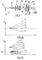
- FIG 1 it schematically represents an installation 10 allowing the bombarding of a layer 20 of material with a beam 30 of ion clusters.
- ions can designate ions that are themselves “pure”, but also species created from several ions and which are electrically charged.
- clusters which will be spoken of below are globally ionised, that meaning that they have an electric charge other than 0.
- these clusters can further comprise ions of other species, including molecules.
- the layer 20 is of semiconductor material. As will be explained below, it can either be of silicon or of silicon carbide, or of another semiconductor material (SiO2 or Si3N4 for example).
- the installation 10 comprises a source 101 of pressurised gas, capable of generating a parallel beam of gas ion clusters from a plasma that is internal to the source 101.
- control of the characteristics of this plasma allows for the defining of the configuration of the ion clusters, more precisely, the control of the pressure of the plasma of the source 101 allows for the controlling of the average number of ions present in the clusters, as will be detailed in reference to figure 3 .
- control of the acceleration voltage allows for the controlling of the speed of these clusters.
- the gas used can for example be argon or nitrogen.
- the layer 20 corresponds to a layer whose surface condition is to be modified in a controlled manner in order to then assemble it, via bonding, with another layer (whose surface condition may also have been adjusted) so as to constitute a detachable substrate.
- ion clusters such as those described above are thus projected onto the surface of the layer 20, this bombardment comprising no chemical reactions.
- the bombardment is said to be purely “ballistic", the bombarded clusters being chemically inert in relation to the material of the layer 20.
- the bombarded clusters are typically made from argon or nitrogen.
- the bombardment is said to be reactive.
- the bombarded ions can in particular be of oxygen or an oxygen compound.
- etching plasma different from the plasma of the source 101
- etching plasma in a zone of the device 10 through which the ion beam will need to pass and which is located in the region of the device 10 that is immediately upstream from the layer 20.
- the material of the surface of the layer 20 and the element making this plasma constitute one of the following pairs: (Si, SF 6 ), (SiC, SF 6 /O 2 ), (SiO 2 , SF 6 /O 2 ), (SiO 2 , CHF 3 /SF 6 ), (Si 3 N 4 , CHF 3 /O 2 /SF 6 ).
- the ion clusters created by the source 101 chemically react with the etching plasma.
- etching plasma itself can also chemically react with the surface of the layer, as well as the species having passed through the etching plasma with the layer itself.
- the ion beam thus generated by the source 101 then passes through an accelerating chamber 102, which allows for the accelerating in the desired manner of the ion clusters of the beam issued from the source 101, thanks to an acceleration electric voltage to which it is possible to give a desired value.
- This beam then passes through a beam-creating electromagnetic structure 103 which allows for the adjusting of the characteristics of the magnetic field of the beam (collimation, focalisation%), via the application of electromagnetic fields with desired characteristics.
- the beam then passes through a magnet annular structure 104 which also allows for the creation of a field with controlled characteristics, in order to selectively deviate the charged species of the ion beam.
- the beam issued from the accelerating chamber 102 and the electromagnetic structure 103 comprises ion clusters of the bombarded species, but also molecules which are electrically neutral (in particular monomers of the bombarded species).
- the trajectory of the different elements of this beam is represented as being strictly rectilinear on the schematic representation in figure 1 .
- these trajectories are not rectilinear, the radius of curvature of the trajectory depending on the mass of the ions and of the different elements of the beam.
- the structure 103 and the structure 104 can be one and the same.
- An electrical neutralising structure 105 is also provided.
- a screen 106 with an opening 1060 is, as has been said, positioned so as to only let through the part of the beam that comprises the desired clusters, so that the latter can have an impact on the layer 20 located behind the opening 1060.
- the screen 106 and its opening 1060 constitute fixed parts of the device.
- the layer 20 only receives the impact of the beam of ion clusters over a basic surface of very small dimensions (the section of the beam passing through the opening 1060 has a width of about one or a few millimetres).
- the layer 20 it is mounted on a movable support 107 whose displacements within the plane perpendicular to the beam, are controlled.
- a screened room 108 is located behind the layer 20 and the means of displacement 107, facing the impact zone of the beam on the layer 20.
- This screened room 108 is connected to means 109 of determining the dose of species received by the layer 20.
- the bombardment of the layer 20 with ion clusters of desired characteristics thus allows for the adjusting of the roughness of the surface of this layer, in view of constituting a detachable substrate.
- the bombardment technique with ion clusters used in the context of this invention allows, as has been said, to very precisely control the impact zone of the ion clusters on the layer 20.
- FIG. 2a it schematically represents several curves C1 to C5 substantially rectilinear, that translate the evolution of the roughness R of the surface of the layer 20, versus the evolution of the voltage V applied to the beam inside the accelerating chamber 102.
- Each of these curves in figure 2a corresponds to a bombardment condition in which the ion clusters mainly comprise a respective number of ions.
- control of the bombardment parameters allows to determine the number of ions present in the clusters bombarded on the layer 20.
- the main parameter that controls the number of ions present in the clusters is the pressure inside the ion source 101.
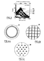
- Each of these curves represents the size repartition of the ion clusters, for a given pressure of the source.
- the size of the clusters is represented by the number of atoms per cluster (upper horizontal scale), which here varies from 0 to 3000 atoms per cluster.
- the lower curve A1 is associated with a pressure of 760 Torr (1 Torr equals 133Pa), the curve A2 with a pressure of 2300 Torr, the curve A3 with a pressure of 3000 Torr, the curve A4 with a pressure of 3800 Torr.
- Each curve in figure 2a thus corresponds to a different value of N: the value of N increases when changing curve, from C1 to C2, to C3, to C4, to C5.
- the curve C1 the highest, corresponds to a bombardment with individual ions, that meaning under conditions where N equals 1.
- the curve C2 immediately below the first curve, corresponds to bombardment conditions under which N has a value greater than 1.
- the next curve C3 illustrates a low increase of the roughness for the same increase in the voltage V.
- the slope of the evolution curves Rf(V) becomes nil, under certain conditions.
- This threshold notably depends on the starting surface condition of the layer, prior to bombardment.
- the bombardment does not increase the surface roughness of the layer 20, but rather reduces it by smoothing this surface.
- the invention uses the bombardment conditions advantageously, in order to adjust the real surface condition of at least one of the layers with which a reversible bonding is required to be made (this adjustment corresponding to augmenting or diminishing the roughness).
- Such an adjustment method is completely specific - it differs, in particular, from those techniques that are only aimed at systematic reduction (and generally the greatest possible) of roughness.
- This influence can be exploited by programming bombardment sequences during which different regions of the layer 20 are subject to bombardments with clusters comprising different numbers of ions, so as to selectively adjust in a desired manner the surface roughness of these different regions.
- the means of displacement 107 will be programmed to displace the layer 20 in conjunction with changes to the parameters allowing to modify the value of N, during the different successive stages of a given bombardment of the layer.
- FIG 2b it again represents the evolution of the surface roughness R of the layer 20 subject to a bombardment with ion clusters comprising an average number N of ions which can vary (here again corresponding to different curves in this figure), versus the acceleration voltage V.
- This figure includes the curves C1 to C5 of figure 2a .
- figure 2b also shows another set of curves C'1 to C'5, which evolve according to the same general logic as the curves C1 to C5 (increase in the number N from curve C'1 to curve C'5, for the same starting layer 20 and the same bombarded ions).
- this smoothing can be very precisely controlled, both in terms of final roughness and in terms of creating a spatial pattern with more or less smooth regions in view of bonding.
- the starting surface condition of the layer 20 is inferior to a given threshold R 0 (which depends among other things on the nature of the material of the layer and of the bombarded species), it will only be possible to increase this roughness.
- FIGS. 4a to 4c they schematically represent layers 20 having been subject to a bombardment with ion clusters such as described above, during which the roughness of certain regions of the surface of the layer has been selectively modified.
- Figure 4a thus represents a layer on the surface of which a ring has been created with a roughness lower than that of the rest of the surface, so as to obtain a greater mechanical stability on this ring at the time of assembling the layer 20 with another layer (homogeneously smooth for example).
- Figures 4b and 4c thus respectively represent a layer 20 with a grid pattern, and with a paved pattern, with a roughness lower than that of the rest of the surface of the layer.
- pattern with variable roughness designates a pattern of which different zones may have different roughness.
- the implementation of the invention thus allows for the very fine controlling of the levels and distributions of roughness on the surface of a layer from which a detachable substrate is to be created after the reversible bonding via molecular adhesion with another layer (whose roughness may have been adjusted if necessary).
Landscapes
- Drying Of Semiconductors (AREA)
- Manufacturing Of Electric Cables (AREA)
- Piezo-Electric Or Mechanical Vibrators, Or Delay Or Filter Circuits (AREA)
- Laminated Bodies (AREA)
- Treatments Of Macromolecular Shaped Articles (AREA)
- Inorganic Insulating Materials (AREA)
- Addition Polymer Or Copolymer, Post-Treatments, Or Chemical Modifications (AREA)
- Silicon Compounds (AREA)
- Glass Compositions (AREA)
- Pressure Welding/Diffusion-Bonding (AREA)
- Micromachines (AREA)
Claims (13)
- Verfahren zur Herstellung von trennbaren Substraten, wobei das Verfahren eine Oberflächenbeschaffenheits-Einstellungsbehandlung von mindestens einer von zwei Schichten des Materials (20), gefolgt von der reversiblen Verbindung der Oberflächen der beiden Schichten zur Herstellung des trennbaren Substrats umfasst, wobei die Oberflächenbeschaffenheits-Einstellungsbehandlung den Beschuss der zu behandelnden Oberfläche mit Ionenclustern umfasst, das Verfahren die Steuerung der Anzahl von Ionen in den Clustern zur Einstellung der Rauheit der zu behandelnden Oberfläche entweder mit dem Ziel der Erhöhung oder der Reduzierung dieser Oberflächenrauheit umfasst, und wobei die zu behandelnde Oberfläche selektiv und lokal in den gewünschten Bereichen durch selektives Ausrichten des Strahls der Ionencluster auf die zu behandelnden Bereiche behandelt wird, um auf dieser Oberfläche eine Struktur zu erzeugen, nach welcher die Rauheit selektiv in der gewünschten Weise eingestellt wird.
- Verfahren gemäß dem vorhergehenden Anspruch, dadurch gekennzeichnet, dass die geschossenen Ionen Spezies umfassen, welche in Bezug auf die zu behandelnde Oberfläche chemisch inert sind.
- Verfahren gemäß dem vorhergehenden Anspruch, dadurch gekennzeichnet, dass die Schicht des Materials, dessen Oberflächenbeschaffenheit eingestellt werden soll, aus Silizium oder aus Siliziumcarbid besteht, und die geschossenen Ionen Argon- oder Stickstoff-Ionen sind.
- Verfahren gemäß einem der drei vorhergehenden Ansprüche, dadurch gekennzeichnet, dass die Ionen Ionen umfassen, welche dazu fähig sind mit dem Material der zu behandelnden Oberfläche eine chemische Reaktion einzugehen.
- Verfahren gemäß dem vorhergehenden Anspruch, dadurch gekennzeichnet, dass der Beschuss aus einem Plasma, welches die Ionen enthält, durchgeführt wird.
- Verfahren gemäß dem vorhergehenden Anspruch, dadurch gekennzeichnet, dass die Materialien der zu behandelnden Oberfläche und des Grundstoffs, welcher das Plasma bildet, eines der folgenden Paare formen: (Si, SF6), (SiC, SF6/O2), (SiO2, SF6/O2), (SiO2, CHF3/SF6), (Si3N4, CHF3/O2/SF6).
- Verfahren gemäß einem der vorhergehenden Ansprüche, dadurch gekennzeichnet, dass die Steuerung derart durchgeführt wird, dass die Oberfläche geglättet wird, um ihre Rauheit auf einen Wert zu bringen, welcher Bindungen über molekulare Adhäsion ermöglicht.
- Verfahren gemäß dem vorhergehenden Anspruch, dadurch gekennzeichnet, dass die Oberfläche eine negative Oberfläche eines SMARTCUT®-artigen Verfahrens ist, welche wiederverwertet wird.
- Verfahren gemäß einem der zwei vorhergehenden Ansprüche, dadurch gekennzeichnet, dass die Steuerung der Anzahl der Ionen durch die Steuerung des Drucks einer Ionenquelle, welche die Erzeugung von Ionenclustern ermöglicht, erreicht wird.
- Verfahren gemäß einem der vorhergehenden Ansprüche, dadurch gekennzeichnet, dass das Verfahren ferner die Steuerung der Beschuss-Spannung, welche auf die Ionen angewandt wird, umfasst.
- Verfahren gemäß einem der vorhergehenden Ansprüche, dadurch gekennzeichnet, dass ein fokussierter Strahl erzeugt wird, der die geschossenen Ionen sowie die Monomer-Spezies dieser Ionen umfasst, und dass der die Ionencluster umfassende Bereich des Strahls auf die Schicht gerichtet wird.
- Verfahren gemäß dem vorhergehenden Anspruch, dadurch gekennzeichnet, dass der Aufprallort des Strahls der Ionencluster auf die Schicht gesteuert wird.
- Verfahren gemäß dem vorhergehenden Anspruch, dadurch gekennzeichnet, dass eine ausreichende räumliche Struktur auf der Oberfläche der Schicht mit einer eingestellten Rauheit, im Vergleich zum Rest der Oberfläche der Schicht, erzeugt wird.
Applications Claiming Priority (3)
| Application Number | Priority Date | Filing Date | Title |
|---|---|---|---|
| FR0213582A FR2846788B1 (fr) | 2002-10-30 | 2002-10-30 | Procede de fabrication de substrats demontables |
| FR0213582 | 2002-10-30 | ||
| PCT/IB2003/005296 WO2004040476A1 (en) | 2002-10-30 | 2003-10-29 | Manufacturing process of detachable substrates |
Publications (2)
| Publication Number | Publication Date |
|---|---|
| EP1556888A1 EP1556888A1 (de) | 2005-07-27 |
| EP1556888B1 true EP1556888B1 (de) | 2011-03-16 |
Family
ID=32104308
Family Applications (1)
| Application Number | Title | Priority Date | Filing Date |
|---|---|---|---|
| EP03809826A Expired - Lifetime EP1556888B1 (de) | 2002-10-30 | 2003-10-29 | Verfahren zur herstellung von abtrennbaren substraten |
Country Status (9)
| Country | Link |
|---|---|
| US (1) | US7056809B2 (de) |
| EP (1) | EP1556888B1 (de) |
| JP (1) | JP4541150B2 (de) |
| AT (1) | ATE502394T1 (de) |
| AU (1) | AU2003276623A1 (de) |
| DE (1) | DE60336410D1 (de) |
| FR (1) | FR2846788B1 (de) |
| TW (1) | TWI281187B (de) |
| WO (1) | WO2004040476A1 (de) |
Families Citing this family (26)
| Publication number | Priority date | Publication date | Assignee | Title |
|---|---|---|---|---|
| US7166524B2 (en) * | 2000-08-11 | 2007-01-23 | Applied Materials, Inc. | Method for ion implanting insulator material to reduce dielectric constant |
| US7223676B2 (en) * | 2002-06-05 | 2007-05-29 | Applied Materials, Inc. | Very low temperature CVD process with independently variable conformality, stress and composition of the CVD layer |
| US7294563B2 (en) * | 2000-08-10 | 2007-11-13 | Applied Materials, Inc. | Semiconductor on insulator vertical transistor fabrication and doping process |
| US6939434B2 (en) * | 2000-08-11 | 2005-09-06 | Applied Materials, Inc. | Externally excited torroidal plasma source with magnetic control of ion distribution |
| US6893907B2 (en) * | 2002-06-05 | 2005-05-17 | Applied Materials, Inc. | Fabrication of silicon-on-insulator structure using plasma immersion ion implantation |
| US20070042580A1 (en) * | 2000-08-10 | 2007-02-22 | Amir Al-Bayati | Ion implanted insulator material with reduced dielectric constant |
| US7465478B2 (en) * | 2000-08-11 | 2008-12-16 | Applied Materials, Inc. | Plasma immersion ion implantation process |
| US7183177B2 (en) * | 2000-08-11 | 2007-02-27 | Applied Materials, Inc. | Silicon-on-insulator wafer transfer method using surface activation plasma immersion ion implantation for wafer-to-wafer adhesion enhancement |
| US7288491B2 (en) * | 2000-08-11 | 2007-10-30 | Applied Materials, Inc. | Plasma immersion ion implantation process |
| US7094670B2 (en) * | 2000-08-11 | 2006-08-22 | Applied Materials, Inc. | Plasma immersion ion implantation process |
| US7320734B2 (en) * | 2000-08-11 | 2008-01-22 | Applied Materials, Inc. | Plasma immersion ion implantation system including a plasma source having low dissociation and low minimum plasma voltage |
| US20050230047A1 (en) * | 2000-08-11 | 2005-10-20 | Applied Materials, Inc. | Plasma immersion ion implantation apparatus |
| US7303982B2 (en) * | 2000-08-11 | 2007-12-04 | Applied Materials, Inc. | Plasma immersion ion implantation process using an inductively coupled plasma source having low dissociation and low minimum plasma voltage |
| US7137354B2 (en) * | 2000-08-11 | 2006-11-21 | Applied Materials, Inc. | Plasma immersion ion implantation apparatus including a plasma source having low dissociation and low minimum plasma voltage |
| US7037813B2 (en) * | 2000-08-11 | 2006-05-02 | Applied Materials, Inc. | Plasma immersion ion implantation process using a capacitively coupled plasma source having low dissociation and low minimum plasma voltage |
| US7341330B2 (en) | 2005-02-28 | 2008-03-11 | Silverbrook Research Pty Ltd | Substrates adapted for adhesive bonding |
| US7425052B2 (en) | 2005-02-28 | 2008-09-16 | Silverbrook Research Pty Ltd | Printhead assembly having improved adhesive bond strength |
| US7468284B2 (en) | 2005-02-28 | 2008-12-23 | Silverbrook Research Pty Ltd | Method of bonding substrates |
| JP4225510B2 (ja) * | 2005-07-06 | 2009-02-18 | 昭和電工株式会社 | 化合物半導体発光ダイオードおよびその製造方法 |
| US20070023850A1 (en) * | 2005-07-30 | 2007-02-01 | Chien-Hua Chen | Bonding surfaces together via plasma treatment on both surfaces with wet treatment on only one surface |
| EP2128891B1 (de) | 2007-02-28 | 2015-09-02 | Shin-Etsu Chemical Co., Ltd. | Prozess zum herstellen eines laminierten substrats |
| JP5143477B2 (ja) * | 2007-05-31 | 2013-02-13 | 信越化学工業株式会社 | Soiウエーハの製造方法 |
| KR101031010B1 (ko) * | 2008-10-29 | 2011-04-25 | 삼성메디슨 주식회사 | 피씨비 및 이를 구비하는 프로브 |
| US7927975B2 (en) | 2009-02-04 | 2011-04-19 | Micron Technology, Inc. | Semiconductor material manufacture |
| US10825685B2 (en) * | 2010-08-23 | 2020-11-03 | Exogenesis Corporation | Method for neutral beam processing based on gas cluster ion beam technology and articles produced thereby |
| JP6042658B2 (ja) * | 2011-09-07 | 2016-12-14 | トヨタ自動車株式会社 | SiC半導体素子の製造方法 |
Family Cites Families (13)
| Publication number | Priority date | Publication date | Assignee | Title |
|---|---|---|---|---|
| JPS6271271A (ja) * | 1985-09-24 | 1987-04-01 | Sharp Corp | 炭化珪素半導体の電極構造 |
| US5354695A (en) * | 1992-04-08 | 1994-10-11 | Leedy Glenn J | Membrane dielectric isolation IC fabrication |
| AU9296098A (en) * | 1997-08-29 | 1999-03-16 | Sharon N. Farrens | In situ plasma wafer bonding method |
| US6153495A (en) * | 1998-03-09 | 2000-11-28 | Intersil Corporation | Advanced methods for making semiconductor devices by low temperature direct bonding |
| DE19818962A1 (de) * | 1998-04-28 | 1999-11-04 | Degussa | Verfahren zum Verbinden zweier Festkörper und das so hergestellte Bauelement |
| US6375790B1 (en) * | 1999-07-19 | 2002-04-23 | Epion Corporation | Adaptive GCIB for smoothing surfaces |
| FR2797347B1 (fr) * | 1999-08-04 | 2001-11-23 | Commissariat Energie Atomique | Procede de transfert d'une couche mince comportant une etape de surfragililisation |
| US6902987B1 (en) * | 2000-02-16 | 2005-06-07 | Ziptronix, Inc. | Method for low temperature bonding and bonded structure |
| WO2002005315A2 (en) * | 2000-07-10 | 2002-01-17 | Epion Corporation | System and method for improving thin films by gas cluster ion be am processing |
| FR2823599B1 (fr) | 2001-04-13 | 2004-12-17 | Commissariat Energie Atomique | Substrat demomtable a tenue mecanique controlee et procede de realisation |
| FR2823596B1 (fr) | 2001-04-13 | 2004-08-20 | Commissariat Energie Atomique | Substrat ou structure demontable et procede de realisation |
| JP3881562B2 (ja) * | 2002-02-22 | 2007-02-14 | 三井造船株式会社 | SiCモニタウェハ製造方法 |
| TWI233154B (en) * | 2002-12-06 | 2005-05-21 | Soitec Silicon On Insulator | Method for recycling a substrate |
-
2002
- 2002-10-30 FR FR0213582A patent/FR2846788B1/fr not_active Expired - Lifetime
-
2003
- 2003-10-29 JP JP2004547930A patent/JP4541150B2/ja not_active Expired - Lifetime
- 2003-10-29 AT AT03809826T patent/ATE502394T1/de not_active IP Right Cessation
- 2003-10-29 EP EP03809826A patent/EP1556888B1/de not_active Expired - Lifetime
- 2003-10-29 AU AU2003276623A patent/AU2003276623A1/en not_active Abandoned
- 2003-10-29 WO PCT/IB2003/005296 patent/WO2004040476A1/en not_active Ceased
- 2003-10-29 DE DE60336410T patent/DE60336410D1/de not_active Expired - Lifetime
- 2003-10-30 TW TW092130185A patent/TWI281187B/zh not_active IP Right Cessation
- 2003-10-30 US US10/695,938 patent/US7056809B2/en not_active Expired - Lifetime
Also Published As
| Publication number | Publication date |
|---|---|
| WO2004040476A9 (en) | 2004-06-24 |
| JP2006505122A (ja) | 2006-02-09 |
| TW200421417A (en) | 2004-10-16 |
| ATE502394T1 (de) | 2011-04-15 |
| WO2004040476A1 (en) | 2004-05-13 |
| AU2003276623A8 (en) | 2004-05-25 |
| AU2003276623A1 (en) | 2004-05-25 |
| US7056809B2 (en) | 2006-06-06 |
| EP1556888A1 (de) | 2005-07-27 |
| US20040092084A1 (en) | 2004-05-13 |
| TWI281187B (en) | 2007-05-11 |
| DE60336410D1 (de) | 2011-04-28 |
| JP4541150B2 (ja) | 2010-09-08 |
| FR2846788A1 (fr) | 2004-05-07 |
| FR2846788B1 (fr) | 2005-06-17 |
Similar Documents
| Publication | Publication Date | Title |
|---|---|---|
| EP1556888B1 (de) | Verfahren zur herstellung von abtrennbaren substraten | |
| US6127273A (en) | Process for anisotropic plasma etching of different substrates | |
| US5314575A (en) | Etching method and apparatus | |
| JP4845936B2 (ja) | 液相エッチング装置 | |
| JP3572081B2 (ja) | 水蒸気増強型荷電粒子線加工方法 | |
| US4734158A (en) | Molecular beam etching system and method | |
| US20120258600A1 (en) | Method and system for post-etch treatment of patterned substrate features | |
| AU4047500A (en) | Reactive ion beam etching method and a thin film head fabricated using the method | |
| US20040173313A1 (en) | Fire polished showerhead electrode | |
| JP2018533214A (ja) | ガスクラスタイオンビーム技術に基づく中性ビーム処理を用いて極めて浅くエッチングする方法 | |
| KR100445105B1 (ko) | 가스 클러스터 이온빔을 이용한 아이.티.오 박막 표면처리시스템 및 그 방법 | |
| JPH04253328A (ja) | 表面処理装置 | |
| JPH022102A (ja) | 半導体素子の製造方法 | |
| KR20000077197A (ko) | 이온주입기의 실리콘-코팅된 표면을 세척하는 시스템과 방법 | |
| WO2019164927A1 (en) | Method to achieve a sidewall etch | |
| CN1135438C (zh) | 三维蚀刻方法 | |
| US4406733A (en) | Dry etching method | |
| US20030015497A1 (en) | Method of etching ferroelectric material | |
| US6165688A (en) | Method of fabricating of structures by metastable atom impact desorption of a passivating layer | |
| CN116988065B (zh) | 一种类光栅结构金属电极制造方法和电极 | |
| US20070181529A1 (en) | Corona discharge plasma source devices, and various systems and methods of using same | |
| JPH0770510B2 (ja) | プラズマ処理装置 | |
| JP2002043277A (ja) | 半導体装置の製造方法、及びそれに用いるプラズマエッチング装置 | |
| JPS62249420A (ja) | プラズマ処理装置 | |
| KR20250168887A (ko) | 기판에 트랩된 전하를 제거하는 방법 및 장치 |
Legal Events
| Date | Code | Title | Description |
|---|---|---|---|
| PUAI | Public reference made under article 153(3) epc to a published international application that has entered the european phase |
Free format text: ORIGINAL CODE: 0009012 |
|
| 17P | Request for examination filed |
Effective date: 20050427 |
|
| AK | Designated contracting states |
Kind code of ref document: A1 Designated state(s): AT BE BG CH CY CZ DE DK EE ES FI FR GB GR HU IE IT LI LU MC NL PT RO SE SI SK TR |
|
| AX | Request for extension of the european patent |
Extension state: AL LT LV MK |
|
| DAX | Request for extension of the european patent (deleted) | ||
| 17Q | First examination report despatched |
Effective date: 20090706 |
|
| GRAP | Despatch of communication of intention to grant a patent |
Free format text: ORIGINAL CODE: EPIDOSNIGR1 |
|
| GRAS | Grant fee paid |
Free format text: ORIGINAL CODE: EPIDOSNIGR3 |
|
| GRAA | (expected) grant |
Free format text: ORIGINAL CODE: 0009210 |
|
| AK | Designated contracting states |
Kind code of ref document: B1 Designated state(s): AT BE BG CH CY CZ DE DK EE ES FI FR GB GR HU IE IT LI LU MC NL PT RO SE SI SK TR |
|
| REG | Reference to a national code |
Ref country code: GB Ref legal event code: FG4D |
|
| REG | Reference to a national code |
Ref country code: CH Ref legal event code: EP |
|
| REG | Reference to a national code |
Ref country code: IE Ref legal event code: FG4D |
|
| REF | Corresponds to: |
Ref document number: 60336410 Country of ref document: DE Date of ref document: 20110428 Kind code of ref document: P |
|
| REG | Reference to a national code |
Ref country code: DE Ref legal event code: R096 Ref document number: 60336410 Country of ref document: DE Effective date: 20110428 |
|
| REG | Reference to a national code |
Ref country code: NL Ref legal event code: VDEP Effective date: 20110316 |
|
| PG25 | Lapsed in a contracting state [announced via postgrant information from national office to epo] |
Ref country code: GR Free format text: LAPSE BECAUSE OF FAILURE TO SUBMIT A TRANSLATION OF THE DESCRIPTION OR TO PAY THE FEE WITHIN THE PRESCRIBED TIME-LIMIT Effective date: 20110617 Ref country code: ES Free format text: LAPSE BECAUSE OF FAILURE TO SUBMIT A TRANSLATION OF THE DESCRIPTION OR TO PAY THE FEE WITHIN THE PRESCRIBED TIME-LIMIT Effective date: 20110627 Ref country code: SE Free format text: LAPSE BECAUSE OF FAILURE TO SUBMIT A TRANSLATION OF THE DESCRIPTION OR TO PAY THE FEE WITHIN THE PRESCRIBED TIME-LIMIT Effective date: 20110316 |
|
| PG25 | Lapsed in a contracting state [announced via postgrant information from national office to epo] |
Ref country code: CY Free format text: LAPSE BECAUSE OF FAILURE TO SUBMIT A TRANSLATION OF THE DESCRIPTION OR TO PAY THE FEE WITHIN THE PRESCRIBED TIME-LIMIT Effective date: 20110316 Ref country code: FI Free format text: LAPSE BECAUSE OF FAILURE TO SUBMIT A TRANSLATION OF THE DESCRIPTION OR TO PAY THE FEE WITHIN THE PRESCRIBED TIME-LIMIT Effective date: 20110316 Ref country code: SI Free format text: LAPSE BECAUSE OF FAILURE TO SUBMIT A TRANSLATION OF THE DESCRIPTION OR TO PAY THE FEE WITHIN THE PRESCRIBED TIME-LIMIT Effective date: 20110316 Ref country code: BG Free format text: LAPSE BECAUSE OF FAILURE TO SUBMIT A TRANSLATION OF THE DESCRIPTION OR TO PAY THE FEE WITHIN THE PRESCRIBED TIME-LIMIT Effective date: 20110616 Ref country code: AT Free format text: LAPSE BECAUSE OF FAILURE TO SUBMIT A TRANSLATION OF THE DESCRIPTION OR TO PAY THE FEE WITHIN THE PRESCRIBED TIME-LIMIT Effective date: 20110316 |
|
| PG25 | Lapsed in a contracting state [announced via postgrant information from national office to epo] |
Ref country code: BE Free format text: LAPSE BECAUSE OF FAILURE TO SUBMIT A TRANSLATION OF THE DESCRIPTION OR TO PAY THE FEE WITHIN THE PRESCRIBED TIME-LIMIT Effective date: 20110316 |
|
| PG25 | Lapsed in a contracting state [announced via postgrant information from national office to epo] |
Ref country code: EE Free format text: LAPSE BECAUSE OF FAILURE TO SUBMIT A TRANSLATION OF THE DESCRIPTION OR TO PAY THE FEE WITHIN THE PRESCRIBED TIME-LIMIT Effective date: 20110316 Ref country code: PT Free format text: LAPSE BECAUSE OF FAILURE TO SUBMIT A TRANSLATION OF THE DESCRIPTION OR TO PAY THE FEE WITHIN THE PRESCRIBED TIME-LIMIT Effective date: 20110718 |
|
| PG25 | Lapsed in a contracting state [announced via postgrant information from national office to epo] |
Ref country code: SK Free format text: LAPSE BECAUSE OF FAILURE TO SUBMIT A TRANSLATION OF THE DESCRIPTION OR TO PAY THE FEE WITHIN THE PRESCRIBED TIME-LIMIT Effective date: 20110316 Ref country code: CZ Free format text: LAPSE BECAUSE OF FAILURE TO SUBMIT A TRANSLATION OF THE DESCRIPTION OR TO PAY THE FEE WITHIN THE PRESCRIBED TIME-LIMIT Effective date: 20110316 Ref country code: RO Free format text: LAPSE BECAUSE OF FAILURE TO SUBMIT A TRANSLATION OF THE DESCRIPTION OR TO PAY THE FEE WITHIN THE PRESCRIBED TIME-LIMIT Effective date: 20110316 |
|
| PG25 | Lapsed in a contracting state [announced via postgrant information from national office to epo] |
Ref country code: NL Free format text: LAPSE BECAUSE OF FAILURE TO SUBMIT A TRANSLATION OF THE DESCRIPTION OR TO PAY THE FEE WITHIN THE PRESCRIBED TIME-LIMIT Effective date: 20110316 |
|
| PLBE | No opposition filed within time limit |
Free format text: ORIGINAL CODE: 0009261 |
|
| STAA | Information on the status of an ep patent application or granted ep patent |
Free format text: STATUS: NO OPPOSITION FILED WITHIN TIME LIMIT |
|
| 26N | No opposition filed |
Effective date: 20111219 |
|
| PG25 | Lapsed in a contracting state [announced via postgrant information from national office to epo] |
Ref country code: DK Free format text: LAPSE BECAUSE OF FAILURE TO SUBMIT A TRANSLATION OF THE DESCRIPTION OR TO PAY THE FEE WITHIN THE PRESCRIBED TIME-LIMIT Effective date: 20110316 |
|
| REG | Reference to a national code |
Ref country code: DE Ref legal event code: R097 Ref document number: 60336410 Country of ref document: DE Effective date: 20111219 |
|
| PG25 | Lapsed in a contracting state [announced via postgrant information from national office to epo] |
Ref country code: IT Free format text: LAPSE BECAUSE OF FAILURE TO SUBMIT A TRANSLATION OF THE DESCRIPTION OR TO PAY THE FEE WITHIN THE PRESCRIBED TIME-LIMIT Effective date: 20110316 Ref country code: MC Free format text: LAPSE BECAUSE OF NON-PAYMENT OF DUE FEES Effective date: 20111031 |
|
| REG | Reference to a national code |
Ref country code: CH Ref legal event code: PL |
|
| GBPC | Gb: european patent ceased through non-payment of renewal fee |
Effective date: 20111029 |
|
| PG25 | Lapsed in a contracting state [announced via postgrant information from national office to epo] |
Ref country code: CH Free format text: LAPSE BECAUSE OF NON-PAYMENT OF DUE FEES Effective date: 20111031 Ref country code: LI Free format text: LAPSE BECAUSE OF NON-PAYMENT OF DUE FEES Effective date: 20111031 |
|
| REG | Reference to a national code |
Ref country code: IE Ref legal event code: MM4A |
|
| PG25 | Lapsed in a contracting state [announced via postgrant information from national office to epo] |
Ref country code: GB Free format text: LAPSE BECAUSE OF NON-PAYMENT OF DUE FEES Effective date: 20111029 |
|
| REG | Reference to a national code |
Ref country code: DE Ref legal event code: R082 Ref document number: 60336410 Country of ref document: DE Representative=s name: VOSSIUS & PARTNER, DE |
|
| REG | Reference to a national code |
Ref country code: DE Ref legal event code: R082 Ref document number: 60336410 Country of ref document: DE Representative=s name: VOSSIUS & PARTNER, DE Effective date: 20120905 Ref country code: DE Ref legal event code: R081 Ref document number: 60336410 Country of ref document: DE Owner name: SOITEC, FR Free format text: FORMER OWNER: S.O.I.TEC SILICON ON INSULATOR TECHNOLOGIES, BERNIN, FR Effective date: 20120905 Ref country code: DE Ref legal event code: R082 Ref document number: 60336410 Country of ref document: DE Representative=s name: VOSSIUS & PARTNER PATENTANWAELTE RECHTSANWAELT, DE Effective date: 20120905 |
|
| PG25 | Lapsed in a contracting state [announced via postgrant information from national office to epo] |
Ref country code: IE Free format text: LAPSE BECAUSE OF NON-PAYMENT OF DUE FEES Effective date: 20111029 |
|
| PG25 | Lapsed in a contracting state [announced via postgrant information from national office to epo] |
Ref country code: LU Free format text: LAPSE BECAUSE OF NON-PAYMENT OF DUE FEES Effective date: 20111029 |
|
| PG25 | Lapsed in a contracting state [announced via postgrant information from national office to epo] |
Ref country code: TR Free format text: LAPSE BECAUSE OF FAILURE TO SUBMIT A TRANSLATION OF THE DESCRIPTION OR TO PAY THE FEE WITHIN THE PRESCRIBED TIME-LIMIT Effective date: 20110316 |
|
| PG25 | Lapsed in a contracting state [announced via postgrant information from national office to epo] |
Ref country code: HU Free format text: LAPSE BECAUSE OF FAILURE TO SUBMIT A TRANSLATION OF THE DESCRIPTION OR TO PAY THE FEE WITHIN THE PRESCRIBED TIME-LIMIT Effective date: 20110316 |
|
| REG | Reference to a national code |
Ref country code: FR Ref legal event code: PLFP Year of fee payment: 14 |
|
| REG | Reference to a national code |
Ref country code: FR Ref legal event code: PLFP Year of fee payment: 15 |
|
| REG | Reference to a national code |
Ref country code: FR Ref legal event code: PLFP Year of fee payment: 16 |
|
| PGFP | Annual fee paid to national office [announced via postgrant information from national office to epo] |
Ref country code: FR Payment date: 20220921 Year of fee payment: 20 |
|
| PGFP | Annual fee paid to national office [announced via postgrant information from national office to epo] |
Ref country code: DE Payment date: 20220906 Year of fee payment: 20 |
|
| REG | Reference to a national code |
Ref country code: DE Ref legal event code: R071 Ref document number: 60336410 Country of ref document: DE |