EP1600928A1 - Flüssigkristallanzeige - Google Patents
Flüssigkristallanzeige Download PDFInfo
- Publication number
- EP1600928A1 EP1600928A1 EP04706818A EP04706818A EP1600928A1 EP 1600928 A1 EP1600928 A1 EP 1600928A1 EP 04706818 A EP04706818 A EP 04706818A EP 04706818 A EP04706818 A EP 04706818A EP 1600928 A1 EP1600928 A1 EP 1600928A1
- Authority
- EP
- European Patent Office
- Prior art keywords
- liquid crystal
- display
- crystal display
- gradation voltage
- period
- Prior art date
- Legal status (The legal status is an assumption and is not a legal conclusion. Google has not performed a legal analysis and makes no representation as to the accuracy of the status listed.)
- Withdrawn
Links
Images





Classifications
-
- G—PHYSICS
- G02—OPTICS
- G02F—OPTICAL DEVICES OR ARRANGEMENTS FOR THE CONTROL OF LIGHT BY MODIFICATION OF THE OPTICAL PROPERTIES OF THE MEDIA OF THE ELEMENTS INVOLVED THEREIN; NON-LINEAR OPTICS; FREQUENCY-CHANGING OF LIGHT; OPTICAL LOGIC ELEMENTS; OPTICAL ANALOGUE/DIGITAL CONVERTERS
- G02F1/00—Devices or arrangements for the control of the intensity, colour, phase, polarisation or direction of light arriving from an independent light source, e.g. switching, gating or modulating; Non-linear optics
- G02F1/01—Devices or arrangements for the control of the intensity, colour, phase, polarisation or direction of light arriving from an independent light source, e.g. switching, gating or modulating; Non-linear optics for the control of the intensity, phase, polarisation or colour
- G02F1/13—Devices or arrangements for the control of the intensity, colour, phase, polarisation or direction of light arriving from an independent light source, e.g. switching, gating or modulating; Non-linear optics for the control of the intensity, phase, polarisation or colour based on liquid crystals, e.g. single liquid crystal display cells
- G02F1/133—Constructional arrangements; Operation of liquid crystal cells; Circuit arrangements
-
- G—PHYSICS
- G09—EDUCATION; CRYPTOGRAPHY; DISPLAY; ADVERTISING; SEALS
- G09G—ARRANGEMENTS OR CIRCUITS FOR CONTROL OF INDICATING DEVICES USING STATIC MEANS TO PRESENT VARIABLE INFORMATION
- G09G3/00—Control arrangements or circuits, of interest only in connection with visual indicators other than cathode-ray tubes
- G09G3/20—Control arrangements or circuits, of interest only in connection with visual indicators other than cathode-ray tubes for presentation of an assembly of a number of characters, e.g. a page, by composing the assembly by combination of individual elements arranged in a matrix no fixed position being assigned to or needed to be assigned to the individual characters or partial characters
- G09G3/34—Control arrangements or circuits, of interest only in connection with visual indicators other than cathode-ray tubes for presentation of an assembly of a number of characters, e.g. a page, by composing the assembly by combination of individual elements arranged in a matrix no fixed position being assigned to or needed to be assigned to the individual characters or partial characters by control of light from an independent source
- G09G3/36—Control arrangements or circuits, of interest only in connection with visual indicators other than cathode-ray tubes for presentation of an assembly of a number of characters, e.g. a page, by composing the assembly by combination of individual elements arranged in a matrix no fixed position being assigned to or needed to be assigned to the individual characters or partial characters by control of light from an independent source using liquid crystals
- G09G3/3611—Control of matrices with row and column drivers
-
- G—PHYSICS
- G09—EDUCATION; CRYPTOGRAPHY; DISPLAY; ADVERTISING; SEALS
- G09G—ARRANGEMENTS OR CIRCUITS FOR CONTROL OF INDICATING DEVICES USING STATIC MEANS TO PRESENT VARIABLE INFORMATION
- G09G3/00—Control arrangements or circuits, of interest only in connection with visual indicators other than cathode-ray tubes
- G09G3/20—Control arrangements or circuits, of interest only in connection with visual indicators other than cathode-ray tubes for presentation of an assembly of a number of characters, e.g. a page, by composing the assembly by combination of individual elements arranged in a matrix no fixed position being assigned to or needed to be assigned to the individual characters or partial characters
-
- G—PHYSICS
- G09—EDUCATION; CRYPTOGRAPHY; DISPLAY; ADVERTISING; SEALS
- G09G—ARRANGEMENTS OR CIRCUITS FOR CONTROL OF INDICATING DEVICES USING STATIC MEANS TO PRESENT VARIABLE INFORMATION
- G09G3/00—Control arrangements or circuits, of interest only in connection with visual indicators other than cathode-ray tubes
- G09G3/20—Control arrangements or circuits, of interest only in connection with visual indicators other than cathode-ray tubes for presentation of an assembly of a number of characters, e.g. a page, by composing the assembly by combination of individual elements arranged in a matrix no fixed position being assigned to or needed to be assigned to the individual characters or partial characters
- G09G3/34—Control arrangements or circuits, of interest only in connection with visual indicators other than cathode-ray tubes for presentation of an assembly of a number of characters, e.g. a page, by composing the assembly by combination of individual elements arranged in a matrix no fixed position being assigned to or needed to be assigned to the individual characters or partial characters by control of light from an independent source
- G09G3/36—Control arrangements or circuits, of interest only in connection with visual indicators other than cathode-ray tubes for presentation of an assembly of a number of characters, e.g. a page, by composing the assembly by combination of individual elements arranged in a matrix no fixed position being assigned to or needed to be assigned to the individual characters or partial characters by control of light from an independent source using liquid crystals
-
- G—PHYSICS
- G09—EDUCATION; CRYPTOGRAPHY; DISPLAY; ADVERTISING; SEALS
- G09G—ARRANGEMENTS OR CIRCUITS FOR CONTROL OF INDICATING DEVICES USING STATIC MEANS TO PRESENT VARIABLE INFORMATION
- G09G2310/00—Command of the display device
- G09G2310/06—Details of flat display driving waveforms
- G09G2310/061—Details of flat display driving waveforms for resetting or blanking
-
- G—PHYSICS
- G09—EDUCATION; CRYPTOGRAPHY; DISPLAY; ADVERTISING; SEALS
- G09G—ARRANGEMENTS OR CIRCUITS FOR CONTROL OF INDICATING DEVICES USING STATIC MEANS TO PRESENT VARIABLE INFORMATION
- G09G2320/00—Control of display operating conditions
- G09G2320/02—Improving the quality of display appearance
- G09G2320/0247—Flicker reduction other than flicker reduction circuits used for single beam cathode-ray tubes
-
- G—PHYSICS
- G09—EDUCATION; CRYPTOGRAPHY; DISPLAY; ADVERTISING; SEALS
- G09G—ARRANGEMENTS OR CIRCUITS FOR CONTROL OF INDICATING DEVICES USING STATIC MEANS TO PRESENT VARIABLE INFORMATION
- G09G2320/00—Control of display operating conditions
- G09G2320/02—Improving the quality of display appearance
- G09G2320/0252—Improving the response speed
-
- G—PHYSICS
- G09—EDUCATION; CRYPTOGRAPHY; DISPLAY; ADVERTISING; SEALS
- G09G—ARRANGEMENTS OR CIRCUITS FOR CONTROL OF INDICATING DEVICES USING STATIC MEANS TO PRESENT VARIABLE INFORMATION
- G09G2320/00—Control of display operating conditions
- G09G2320/02—Improving the quality of display appearance
- G09G2320/0261—Improving the quality of display appearance in the context of movement of objects on the screen or movement of the observer relative to the screen
-
- G—PHYSICS
- G09—EDUCATION; CRYPTOGRAPHY; DISPLAY; ADVERTISING; SEALS
- G09G—ARRANGEMENTS OR CIRCUITS FOR CONTROL OF INDICATING DEVICES USING STATIC MEANS TO PRESENT VARIABLE INFORMATION
- G09G2320/00—Control of display operating conditions
- G09G2320/06—Adjustment of display parameters
- G09G2320/0613—The adjustment depending on the type of the information to be displayed
-
- G—PHYSICS
- G09—EDUCATION; CRYPTOGRAPHY; DISPLAY; ADVERTISING; SEALS
- G09G—ARRANGEMENTS OR CIRCUITS FOR CONTROL OF INDICATING DEVICES USING STATIC MEANS TO PRESENT VARIABLE INFORMATION
- G09G2320/00—Control of display operating conditions
- G09G2320/06—Adjustment of display parameters
- G09G2320/0673—Adjustment of display parameters for control of gamma adjustment, e.g. selecting another gamma curve
-
- G—PHYSICS
- G09—EDUCATION; CRYPTOGRAPHY; DISPLAY; ADVERTISING; SEALS
- G09G—ARRANGEMENTS OR CIRCUITS FOR CONTROL OF INDICATING DEVICES USING STATIC MEANS TO PRESENT VARIABLE INFORMATION
- G09G3/00—Control arrangements or circuits, of interest only in connection with visual indicators other than cathode-ray tubes
- G09G3/20—Control arrangements or circuits, of interest only in connection with visual indicators other than cathode-ray tubes for presentation of an assembly of a number of characters, e.g. a page, by composing the assembly by combination of individual elements arranged in a matrix no fixed position being assigned to or needed to be assigned to the individual characters or partial characters
- G09G3/2007—Display of intermediate tones
- G09G3/2014—Display of intermediate tones by modulation of the duration of a single pulse during which the logic level remains constant
Definitions
- the present invention relates to a liquid crystal display which displays images by using a liquid crystal display panel. More particularly, the present invention relates to a liquid crystal display capable of improving deterioration of display quality of moving images, which is caused by response characteristics of the liquid crystal display panel.
- An LCD is a display that applies an electric field to a liquid crystal layer having anisotropic permittivity (anisotropic dielectric constant), the liquid crystal layer being interposed between two substrates. By adjusting the electric field, the LCD controls a volume of light passing through the substrates so as to obtain desired image signals.
- the LCD is well known among other flat-panel displays convenient for carriage. Especially, a thin film transistor (TFT) LCD utilizing a TFT as a switching element is predominantly used.
- TFT thin film transistor
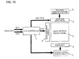
- Fig. 10 is a block diagram illustrating a schematic structure of the conventional liquid crystal display.
- Fig. 10 shows an LCD controller 1, a liquid crystal display panel 2, a signal line drive circuit 3, a scan line drive circuit 4, a reference gradation voltage generation section 5, a backlight 6, and a backlight driving inverter circuit 7.
- Image data is input in the LCD controller 1, as gradation data D11 and synchronous data D12.
- the gradation data D11 is RGB signals, for example.
- the synchronous data D12 includes a vertical synchronizing signal, a horizontal synchronizing signal, a data enable signal (DE), a clock and others.
- the LCD controller 1 Based on the input gradation data D11 and synchronous data D12, the LCD controller 1 generates not only gradation data D13 and a signal-side control signal D14 to be output to the signal line drive circuit 3, but also a scan line control signal D 15 to be output to the scan line drive circuit 4. With this arrangement, the LCD controller 1 controls image display on the liquid crystal display panel 2.
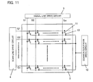
- the liquid crystal display panel 2 has a first and a second glass substrates (not shown). Over the first glass substrate, thin film transistors (TFT) 11 are provided near respective intersections of n scan lines G1 to Gn and m signal lines S1 to Sm.
- TFT 11 is a nonlinear element (switching element).
- Gate lines for the TFTs 11 are connected to the scan lines G1 to Gn.
- Source electrodes are connected to the signal lines S1 to Sm, and drain electrodes are connected to pixel electrodes.
- the second glass substrate is disposed so as to face the first glass substrate, and common electrodes are formed all over the surface of the glass substrate, using transparent electrodes made of ITO and the like.
- Each of the common electrodes is connected to a common electrode drive circuit 12, which defines an electric potential.
- Liquid crystal 13 is interposed between the common electrodes and the pixel electrodes formed on the first glass.
- the scan lines G1 to Gn and the signal lines S1 to Sm are connected to the scan line drive circuit 4 and the signal line drive circuit 3, respectively.
- the scan line drive circuit 4 applies a high voltage to n scan lines G1 to Gn sequentially, so as to carry out scanning and activate the TFT 11 connected to each of the scan lines G1 to Gn.
- the signal line drive circuit 3 outputs gradation voltages corresponding to image data to any of m signal lines S1 to Sm. With this, the gradation voltage is written into the pixel electrodes through the activated TFTs 11. Then, a difference in electric potentials is generated between the common electrodes set at a certain potential and the pixel electrodes where the gradation voltage is applied. With the difference, the volume of light transmission is adjusted.
- the backlight 6 disposed at the back side of the liquid crystal display panel 2 is driven by the inverter circuit 7, so as to emit light with a certain level of brightness. Therefore, according to the aforesaid operating principles of the liquid crystal display panel 2, the volume of transmitted light emitted from the backlight 6 is controlled, so that a desirable image display is realized.
- the reference gradation voltage generation section 5 illustrated in Fig. 10 supplies the signal line drive circuit 3 with a reference gradation voltage.
- a reference gradation voltage is applied to the liquid crystal display panel 2, in accordance with a gradation level of image data.
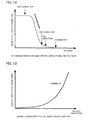
- Fig. 12 is an explanatory view expressing one example of the relationship between the transmittance of the liquid crystal and the applied voltage.
- a reference gradation voltage is defined so that the relationship between the gradation level of the image data and the transmittance draws a curve of gamma 2.2 as plotted in Fig. 13, for example.
- one-eighth of the maximum reference gradation voltage is defined as a reference gradation, for example.
- the rest of the gradation voltages are generated by dividing the adjacent reference gradation voltages. More specifically, all display gradation voltages are defined using divided resistors.
- Fig. 14 is an explanatory view illustrating signal waveforms output from the scan line drive circuit 4 and the signal line drive circuit 3 to the scan lines and the signal lines, respectively, in the conventional liquid crystal display.
- the time is set on the abscissa axis.
- VG1 to VGn are signals output sequentially to n scan lines, by applying a high electric potential (data electric potential) to a single scan line at a time.
- VD is a signal waveform output to a single signal line
- Vcom is a signal waveform applied to common electrodes.
- the VD is a signal that changes in signal intensity corresponding to each image data
- the Vcom is a signal that maintains a certain value and does not change with time.
- the conventional liquid crystal display and its driving method are described above.
- display quality deteriorates, for example, after-image emerges.
- the cause of this problem is a slow response of liquid crystal material.
- the liquid crystal material cannot respond to the change within one field period. Thus, it is assumed that a few field periods are required to respond. To solve this problem, studies about liquid crystal materials and others have been currently implemented.
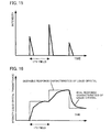
- Figs. 15 and 16 illustrate results of comparing the response time of display light between a CRT and an LCD, in terms of one pixel.
- Fig. 15 plots the response time of the CRT
- Fig. 16 plots the response time of the LCD.
- the CRT is a so-called impulse-type display, which illuminates for only a few milliseconds after an electronic beam hits fluorescent material on the surface of a tube.
- the LCD is a so-called hold-type display, which holds display light during one field period from the completion of writing data into a pixel to the start of writing next data.
- Fig. 17 illustrates one example of a so-called black-writing-type liquid crystal display.
- black display data is written into all over the screen at the same time, so that the black display over the entire screen is carried out for a certain period of time.
- black display data is written into the scan lines sequentially, so that the black display is carried out in part of the screen for a certain period of time. Accordingly, the image display period is shortened compared to the one in the conventional hold-type display (disclosed in Japanese Laid-Open Patent Publication No. 127917/1997 and 109921/1999, Tokukaihei 9-127917 and 11-109921).
- Such a liquid crystal display that has display elements and a shutter is disclosed in Tokukaihei 9-325715, for example.
- the display elements transform electric image signals to image-display light while continuing the transforming operation for a certain display hold period.
- the shutter limits the display hold period to a certain time within one field period, in synchronism with the vertical synchronization of image signals.
- Tokukai 2002-123223 and 2002-318569 Only when moving images are displayed on the liquid crystal display panel, the black display is carried out in at least a part of the screen for a certain period of time, so that the impulse-type display is carried out. As a result, the motion blur emerged in movie display can be restrained. In static display, the hold-type display is carried out without setting the black display period. Thus, deterioration of display quality due to flicker and others is prevented.
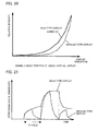
- the relationship between the display gradation and the display brightness that is, so-called gamma characteristics differ between the impulse display mode shown in Figs. 17 and 18 and the normal hold display mode shown in Fig. 19.
- the impulse-type display is carried out by producing the black display in at least part of the screen for a certain period of time.
- Fig. 20 for example, the full line plots gamma characteristic in the hold display mode.
- the dotted line plots gamma characteristics when the motion blur is prevented in the impulse display mode shown in Fig. 18. That is, the black display period is inserted into one field period, so that the image display period is shortened.
- image-display characteristics vary between movie display with the method shown in Figs. 17 and 18 and static display with the method shown in Fig. 19. Thus, display quality significantly deteriorates.
- Fig. 21 the full line plots changes in display brightness with time in the hold display mode.
- the dotted line in Fig. 21 plots changes in display brightness with time when the motion blur is prevented in the impulse display mode illustrated in Fig. 18.
- Fig. 21 clearly shows, the ratio in attained brightness between the methods in low gradation display is different from the ratio in attained brightness between the methods in high gradation display. Therefore, it is considered that the different characteristics in display gradation and display brightness (gamma characteristics) between the display methods come from the differences between the response characteristics of the liquid crystal in the low-gradation display and the response characteristics of the liquid crystal in the high-gradation display.
- An object of the present invention is to provide a liquid crystal display, which can prevent deterioration of display quality by suppressing variations in gamma characteristics, even when a mode for driving a liquid crystal display panel is switched between an impulse drive mode and a hold drive mode.
- the liquid crystal display of the present invention displaying, using a liquid crystal display panel, an image responsive to input image data, includes driving means for driving the liquid crystal display panel in either an impulse drive mode or a hold drive mode, (i) in the impulse drive mode an image display period for performing display according to the input image data, and a monochrome display period for performing display according to previously-specified certain monochrome display data being generated within an input image data rewriting period (e.g.
- the means for varying the gradation voltage varies a reference gradation voltage for driving the liquid crystal display panel.
- the liquid crystal display panel further includes a storage section storing sets of reference gradation voltage data previously specified.
- the liquid crystal display panel further includes means for detecting a temperature in the liquid crystal display; and means for varying a gradation voltage to be applied to the liquid crystal display panel in accordance with the input image data and the detected temperature in the display.
- the switching means switches between the modes for driving the liquid crystal display panel, in accordance with a user's instruction, or in accordance with a result of detecting an amount of movement of the input image data or a result of detecting a status of connection with a device for inputting the input image data.
- a gradation voltage to be applied to the liquid crystal display panel varies corresponding to input image data. Therefore, it is possible to prevent variations in gamma characteristics, which is caused by differences in response speed of the liquid crystal between display gradations, when certain monochrome display is carried out. Thus, it is possible to prevent deterioration of display quality, which occurs when the impulse display mode and the hold display mode are switched.
- the driving means varies a reference gradation voltage itself for driving the liquid crystal display panel.
- a reference gradation voltage itself for driving the liquid crystal display panel.
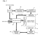
- Fig. 1 is a block diagram illustrating a schematic structure of the liquid crystal display of the present embodiment.
- Fig. 2 is an explanatory diagram illustrating one example of drive signal waveforms in the impulse-type display in the liquid crystal display of the present embodiment.
- Fig. 3 is a schematic explanatory view showing specific examples of the reference gradation voltage data storage section in the liquid crystal display of the present embodiment.
- Fig. 4 is a schematic explanatory view expressing response characteristics of the liquid crystal in the liquid crystal display of the present embodiment.
- Fig. 5 is a block diagram illustrating a schematic structure of the reference gradation voltage generation section in the liquid crystal display of the present embodiment.
- Fig. 6 is a circuit diagram illustrating a schematic structure of primary parts of the signal line drive circuit in the liquid crystal display of the present embodiment.
- Fig. 7 is a schematic explanatory view expressing gamma characteristics in the hold display mode and the impulse display mode in the liquid crystal display according to the present embodiment.
- the liquid crystal display of the present embodiment has a microcomputer 22, a reference gradation voltage data storage section 23, and a backlight control circuit 24 as illustrated in Fig. 1.
- the microcomputer 22 is supplied with a switching signal J1.
- the switching signal J1 is used for switching between the hold-type display displaying input image data throughout one field period (e.g. for 16.7 msec when the vertical display cycle is 60 Hz) and the impulse-type display generating, in one field period, a monochrome display period in which display based on certain monochrome display data is carried out.
- the reference gradation voltage data storage section 23 is, for example, a ROM which stores a plurality of values of reference gradation voltages generated at the reference gradation voltage generation section 5 for each of the display methods (in the impulse-type display or the hold-type display).
- the backlight control circuit 24 controls lighting of the backlight 6 in synchronism with the writing of monochrome display data.
- the microcomputer 22 executes programs stored on storage such as memory (not shown), thereby giving instructions to the LCD controller 21 (drive means) to perform the display methods, and performing control operations so that values of reference gradation voltages corresponding to the display methods can be read out from the reference gradation voltage data storage section (means for varying gradation voltages) 23. Therefore, it is possible to allow a microcomputer (computer), which is capable of controlling the LCD controller (drive means) 21 and the reference gradation voltage data storage section 23, to act as the microcomputer 22, by causing the microcomputer to execute the aforesaid methods.
- the programs executed by the computer are, for instance, distributed in the form of storage mediums storing the programs, or distributed through various wired or wireless channels.
- the switching signal J1 is generated in accordance with user's preference which is manually input using a remote controller (not shown) and others.
- the display methods may be also automatically switched between the movie display and the static display.
- the microcomputer 22 instructs the LCD controller 21 to insert black display data/ perform display, thereby changing whether to carry out the impulse-type display or the hold-type display on the liquid crystal panel 2.
- the switching signal J1 can be generated through a circuit receiving an instruction by a user's manual input (e.g. light-receptive spot on the remote controller (not shown)), or a circuit detecting an automatic switching trigger (e.g. a circuit detecting the amount of movement of input image data or a circuit detecting a status of connection with another device). Also, based on the switching signal J1 from such a circuit, the microcomputer 22 may control the LCD controller 21 and the reference gradation voltage data storage section 23. Alternatively, the microcomputer 22 may control these members 21 and 23, referring to user's instructions or an automatic switching trigger.
- a circuit receiving an instruction by a user's manual input e.g. light-receptive spot on the remote controller (not shown)
- a circuit detecting an automatic switching trigger e.g. a circuit detecting the amount of movement of input image data or a circuit detecting a status of connection with another device.
- the microcomputer 22 may control the LCD controller 21 and the reference gradation voltage data storage section 23.
- the circuit that receives the user's instructions or the microcomputer 22 may receive, as the user's instructions, instructions defining whether or not to carry out the impulse-type display, or determine whether or not the impulse-display is carried out, in response to specified instructions defining in advance the relevance of whether or not to carry out the impulse-display.
- the specified instructions include an instruction for selecting an input image source or for setting an image display mode.
- the microcomputer 22 or the circuit that detects an automatic switching trigger may define whether or not to carry out the impulse-type display, based on the amount of movement detected in the input image data, or based on the presence or absence of the state of connection with a computer (not shown) that mainly generates static images.
- the circuit receiving instructions or the circuit detecting triggers generates the switching signal J1 so as to define whether or not to carry out the impulse-type display.
- the microcomputer 22 controls the members 21 and 23 so as to define whether or not to carry out the impulse-type display.
- scanning signals supplied from the scan line drive circuit 4 to the scan lines G1 to Gn on the liquid crystal display panel 2 have an image data select period T1 and a black display select period T2 within one field period.
- image data select period T1 gradation voltages corresponding to image data are written into the pixel electrodes.
- black display select period T2 a voltage for carrying out the black display is written into the pixel electrode.
- Gradation voltages corresponding to image data and a voltage for carrying out the black display are alternately output to the signal lines S1 to Sm.
- the black display select period T2 is set as about a half of the conventional scan line select period T3 described with reference to Fig. 14.
- the black display is carried out in a scan line locating above or below with a distance for several lines from a scan line, selected in the image data select period T1.
- a voltage corresponding to the black display is applied to the signal lines S1 to Sm during the black display select period T2, so that the black display can be carried out in each of the scan lines.
- a line to which black data is written and a line to which image data is written are selected by suitable control of the scan line drive circuit 4 by the LCD controller 21. As a result, the lines can be scanned sequentially, while the distance for several lines between the image-data written line and the black-data written line is maintained.
- the black display data is inserted between sets of image data for respective fields, inside the LCD controller 21.
- a half of the period for selecting a single line is used for supplying image data to the signal line driver circuit 3, and the rest of the period is used for supplying the black display data to the signal line drive circuit 3.
- the impulse-type display can be realized with 50 percent of the impulse-ratio (ratio of the image display period in one image display cycle).
- Fig. 2 illustrates one example of using the liquid crystal display panel in a normally white mode.
- the present invention is not limited to this, and it is obvious that the liquid crystal display panel in a normally black mode can be also used.
- the conventional example illustrated in Fig. 14 is applied in similar fashion.
- the LCD controller 21 controls the scan line drive circuit 4 not only to supply the signal line drive circuit 3 with input image data, but also to perform line-scanning in each field circle.
- the normal hold-type display can be realized with 100 percent of the impulse ratio.
- the reference gradation voltage generation section 5 supplies the signal line drive circuit 3 with reference gradation voltages, based on the reference gradation voltage data stored in the reference gradation voltage data storage section 23.
- the reference gradation voltage data storage section 23 stores sets of reference gradation voltage data corresponding to the hold display mode and the impulse display mode, respectively, onto separate regions of a ROM.
- One of these sets of reference gradation voltage data is selected and output to the reference gradation voltage generation section 5, according to an instruction from the microcomputer 22.
- the sets of reference gradation voltage data to be stored on the reference gradation voltage data storage section 23 are set as follows.
- reference gradation voltage data corresponding to the hold display mode is set so that the relationship between the display gradation and the display brightness (liquid crystal transmittance) forms gamma 2.2, in accordance with a so-called V-T curve as plotted in Fig. 12
- V-T curve as plotted in Fig. 12
- the number of display signal levels that is, the number of displayed data is 256 gradations for eight bits
- voltage data V0, V32..., V255 corresponding to 0, 32, 64, 96, 128, 160, 192, 224, 255 gradations have been set or stored.
- the reference gradation voltages are linearly divided by resistors, so as to obtain voltages for all gradations to be applied to the liquid crystal display panel 2.
- reference gradation voltage data is not determined directly based on the V-T curve plotted in Fig. 12.
- the reference gradation voltage data is determined by working out the relationship between the intensity integral I and the voltage T applied to the liquid crystal within one field period, while display brightness (transmittance) changes with time during the impulse display mode as plotted in Fig. 4.
- the intensity integral I changes according to the response speed of the liquid crystal.
- the response speed of the liquid crystal changes according to a display gradation. Therefore, in the case of the impulse-type display, the relationship between the applied voltage and the liquid crystal transmittance (intensity) shown in Fig. 12 cannot be held. That is, it is not possible to realize desirable gradation display with the gradation voltage for the hold-type display, which is determined in accordance with the V-T curve in Fig. 12.
- the reference gradation voltage data which is different from the one in the hold-type display, is set so that the relationship between the display gradation and the display brightness (liquid crystal transmittance) can form, for example, the relationship of gamma 2.2.
- the number of display signal levels that is, the number of displayed data is 256 gradations for eight bits
- voltage data V0, V32..., V255 corresponding to 0, 32, 64, 96, 128, 160, 192, 224, 255 gradations are set or stored.
- the reference gradation voltages are linearly divided by resistors, so that voltages for all gradations to be applied to the liquid crystal display panel 2 are obtained.
- the reference gradation voltage generation section 5 causes a DA converter 5a to convert digital data V0, V32, ..., V255 obtained from the reference gradation voltage data storage section 23 into analog data. Then, the reference gradation voltage generation section 5 causes an amplifier 5b to amplify and adjust the reference gradation voltages VA0, VA32,..., VA255 as appropriate, thereby supplying them to the signal line drive circuit 3 including a source driver and others. As illustrated in Fig. 6, in the signal line drive circuit 3, input terminals of the reference gradation voltages VA0, VA32.... VA255 are connected each other by divided resistors. Voltages for all gradations corresponding to image data are generated, so that display in accordance with image data for eight bits is performed.
- the hold display mode in which a ratio of image display period in one field period (impulse ratio) is 100 percent and the impulse display mode in which the ratio is 50 percent are selected in an alternate manner.
- the present invention is not limited to this. Obviously, it is possible to control switching between a plurality of different impulse ratios by setting a suitable black display period.
- the arrangement allows a reference gradation voltage for driving the liquid crystal display panel to be varied, in accordance with each impulse ratio.
- a reference gradation voltage for driving the liquid crystal display panel is varied.
- the gamma characteristics are always maintained at certain levels.
- the present invention is not limited to this.
- a gradation conversion section is provided in a stage prior to the LCD controller 21. Then, a gradation level of image data is converted, so that a gradation voltage to be applied to the liquid crystal display panel 2 is varied according to the input image data. In this case the image data supplied to the LCD controller 21 is actually compressed in bits, so that the display performance deteriorates due to the gradation conversion.
- a reference gradation voltage to be supplied to the signal line drive circuit 3 is adjusted, so that changes in gamma characteristics can be restrained with the display performance for eight bits maintained.
- changes in gamma characteristics can be restrained with the display performance for eight bits maintained.
- Fig. 8 is a block diagram illustrating a schematic structure of the liquid crystal display according to the present embodiment.
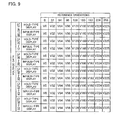
- Fig. 9 is a summary table showing specific example of the reference gradation voltage data storage section in the liquid crystal display of the present embodiment.
- the liquid crystal display of the present embodiment has a temperature sensor 35, a reference gradation voltage data storage section 33, and a microcomputer 32.
- the temperature sensor 35 detects a temperature inside the display.
- the reference gradation voltage data storage section 33 is a ROM, for example, which stores plurality of values of the reference gradation voltages generated by the reference gradation voltage generation section 5, corresponding to the respective temperatures in the display and display methods (the impulse display mode and the hold display mode).
- the microcomputer 32 controls the LCD controller 21 to switch between the display methods (the impulse display mode and the hold display mode), based on the switching signal J1.
- the microcomputer 32 also selects and reads out any one of the sets of reference gradation voltage data stored in the reference gradation voltage data storage section 33, based on the switching signal J1 and in-device temperature data J2 detected by the temperature sensor 35.
- the reference gradation voltage data storage section 33 stores the sets of reference gradation voltage data corresponding to the hold display mode and the impulse display mode under respective temperature conditions, onto separate regions of a ROM.
- One of these sets of reference gradation voltage data is selected and output to the reference gradation voltage generation section 5, according to instructions from the microcomputer 32.
- reference gradation voltage data stored in the reference gradation voltage data storage section 33 is set so that gamma characteristics in the hold display mode is matched with those in the impulse display mode, in the following ranges of temperature; below 10 degrees, 10 to 20 degrees, 20 to 30 degrees, 30 to 40 degrees, 40 to 50 degrees, and above 50 degrees in Celsius, in a similar manner shown in the first embodiment. That is, when the number of display signal levels, that is, the number of display data is 256-gradation for eight bits, 12 sets of gradation voltage data corresponding to nine reference gradations for each a 32-step gradation, 0, 32, 64, 96, 128, 160, 192, 224, and 255, have been set and stored.
- the temperature sensor 35 is preferably provided so as to detect a temperature of the liquid crystal display panel 2 itself as much as possible. A single or even a plurality of the temperature sensors 35 may be provided on inner surfaces of different panels. Also, the ranges of temperature for switching a reference gradation voltage are not limited to the above examples, and it is obvious that the ranges can be set as appropriate.
- any one of plural reference gradation voltage data is read out into the reference gradation voltage generation section 5.
- the plural reference gradation voltage data are stored on the reference gradation voltage storage section 33. Note that the plural reference gradation voltage data are used for carrying out the hold-type display or impulse-type display under each temperature condition. Then, based on the reference gradation voltage data thus read out, a gradation voltage to be applied to the liquid crystal display panel 2 is determined, corresponding to each gradation level of the input image data.
- the hold display mode in which a ratio of image display period in one field period (impulse ratio) is 100 percent and the impulse display mode in which the ratio is 50 percent can be selected alternatively.
- the present invention is not limited to this. Obviously, it is possible to control switching between a plurality of different impulse ratios by setting a suitable black display period.
- the arrangement allows a reference gradation voltage for driving the liquid crystal display panel to be varied, in accordance with each impulse ratio.
- a reference gradation voltage for driving the liquid crystal display panel is varied.
- the gamma characteristics are always maintained at certain levels.
- the present invention is not limited to this.
- a gradation conversion section is provided in a stage prior to the LCD controller 21. Then, a gradation level of image data is converted, so that a gradation voltage to be applied to the liquid crystal display panel 2 can be varied according to the input image data.
- the impulse-type display carrying out the black display for a certain period of time in part of the screen In the first and second embodiments, as shown in Fig. 18, descriptions are given about the impulse-type display carrying out the black display for a certain period of time in part of the screen. It is also possible to apply the above embodiments for the impulse-type display carrying out the black (or another single color) display over the entire screen for a certain period of time, as shown in Fig. 17. It is obvious that the timing for supplying the black display data to each of the scan lines of the liquid crystal display panel is not limited to the above.
- the liquid crystal display of the present invention displays an image corresponding to input image data using the liquid crystal display panel, and has the following three means.
- the first means is to set, within one field period, an image display period for displaying input image data and a monochrome display period for displaying certain monochrome data.
- the second means is to switch the ratio of the image display period within one field period.
- the third means is to vary, in accordance with the ratio of the image display period within one field period, a gradation voltage to be applied to the liquid crystal display panel corresponding to the input image data.
- the means for varying a gradation voltage may vary a reference gradation voltage for driving the liquid crystal display panel.
- the liquid crystal display may have a storage section for storing a plurality of the reference gradation voltage data that is previously specified.
- the liquid crystal display may have still other means for detecting a temperature in display, and means for varying a gradation voltage to be applied to the liquid crystal panel corresponding to input image data, in accordance with the detected in-device temperature.
- a gradation voltage to be applied to the liquid crystal display panel varies corresponding to input image data. Therefore, it is possible to prevent variation in gamma characteristics caused by differences in response speed of the liquid crystal between display gradations, when monochrome display is carried out. Thus, it is possible to prevent deterioration of display quality occurring when the impulse display mode and the hold display mode are switched, for example.
- the reference gradation voltage for driving the liquid crystal display panel can be varied according to the ratio of the image display period within one field period. Therefore, display performance of the liquid crystal display panel can be maintained, so that high-quality display can be realized. Further, by preventing differences in gamma characteristics due to the temperature dependency of the liquid crystal, high-quality display can be always achieved.
- liquid crystal display of the present invention in accordance with a selected drive mode (impulse drive mode or hold drive mode), a gradation voltage to be applied to the liquid crystal display panel varies corresponding to input image data. Therefore, it is possible to prevent variation in gamma characteristics, which is caused by differences in response speed of the liquid crystal between display gradations, when monochrome display is carried out in the impulse drive mode. Thus, high-quality display can be realized, so that the liquid crystal display can be suitably used for various types of devices including liquid crystal TV sets.
Landscapes
- Engineering & Computer Science (AREA)
- Physics & Mathematics (AREA)
- General Physics & Mathematics (AREA)
- Theoretical Computer Science (AREA)
- Computer Hardware Design (AREA)
- Crystallography & Structural Chemistry (AREA)
- Chemical & Material Sciences (AREA)
- Nonlinear Science (AREA)
- Mathematical Physics (AREA)
- Optics & Photonics (AREA)
- Control Of Indicators Other Than Cathode Ray Tubes (AREA)
- Liquid Crystal Display Device Control (AREA)
- Liquid Crystal (AREA)
Applications Claiming Priority (3)
| Application Number | Priority Date | Filing Date | Title |
|---|---|---|---|
| JP2003025636 | 2003-02-03 | ||
| JP2003025636 | 2003-02-03 | ||
| PCT/JP2004/000966 WO2004070697A1 (ja) | 2003-02-03 | 2004-01-30 | 液晶表示装置 |
Publications (2)
| Publication Number | Publication Date |
|---|---|
| EP1600928A1 true EP1600928A1 (de) | 2005-11-30 |
| EP1600928A4 EP1600928A4 (de) | 2006-10-11 |
Family
ID=32844111
Family Applications (1)
| Application Number | Title | Priority Date | Filing Date |
|---|---|---|---|
| EP04706818A Withdrawn EP1600928A4 (de) | 2003-02-03 | 2004-01-30 | Flüssigkristallanzeige |
Country Status (7)
| Country | Link |
|---|---|
| US (1) | US7911430B2 (de) |
| EP (1) | EP1600928A4 (de) |
| JP (1) | JP4397890B2 (de) |
| KR (1) | KR100717229B1 (de) |
| CN (1) | CN100545899C (de) |
| TW (1) | TWI254902B (de) |
| WO (1) | WO2004070697A1 (de) |
Cited By (4)
| Publication number | Priority date | Publication date | Assignee | Title |
|---|---|---|---|---|
| EP1746569A1 (de) * | 2005-07-18 | 2007-01-24 | Samsung Electronics Co., Ltd. | Flüssigkristallanzeige und Ansteuerungsverfahren dafür |
| US7764266B2 (en) | 2006-01-24 | 2010-07-27 | Au Optronics Corporation | Method and system for controlling an active matrix display device |
| US8766906B2 (en) | 2006-12-05 | 2014-07-01 | Semiconductor Energy Laboratory Co., Ltd. | Liquid crystal display device and driving method thereof |
| US9035867B2 (en) | 2007-05-18 | 2015-05-19 | Semiconductor Energy Laboratory Co., Ltd. | Liquid crystal display device and driving method thereof |
Families Citing this family (38)
| Publication number | Priority date | Publication date | Assignee | Title |
|---|---|---|---|---|
| JP2005017566A (ja) * | 2003-06-25 | 2005-01-20 | Sanyo Electric Co Ltd | 表示装置およびその制御方法 |
| TWI322900B (en) * | 2004-07-30 | 2010-04-01 | Au Optronics Corp | Impulse backlight system and a flat display using the same |
| KR101073040B1 (ko) * | 2004-08-20 | 2011-10-12 | 삼성전자주식회사 | 표시장치와, 그의 구동 장치 및 구동 방법 |
| JP2006106689A (ja) | 2004-09-13 | 2006-04-20 | Seiko Epson Corp | 液晶パネルの表示方法、液晶表示装置及び電子機器 |
| TW200623897A (en) * | 2004-12-02 | 2006-07-01 | Seiko Epson Corp | Image display method, image display device, and projector |
| US20060187160A1 (en) * | 2005-02-24 | 2006-08-24 | Lai Chih C | Method for solving feed-through effect |
| JP2006301053A (ja) * | 2005-04-18 | 2006-11-02 | Renesas Technology Corp | 液晶表示装置 |
| TWI260568B (en) * | 2005-07-15 | 2006-08-21 | Au Optronics Corp | Driving system and method for liquid crystal display |
| CN100359557C (zh) * | 2005-08-04 | 2008-01-02 | 友达光电股份有限公司 | 液晶驱动系统与方法 |
| KR20070040999A (ko) * | 2005-10-13 | 2007-04-18 | 삼성전자주식회사 | 자동 감마 및 휘도 보정 기능을 갖는 액정 표시 장치 |
| JP3953507B2 (ja) * | 2005-10-18 | 2007-08-08 | シャープ株式会社 | 液晶表示装置 |
| JP4762681B2 (ja) * | 2005-11-07 | 2011-08-31 | ローム株式会社 | Ledドライバ及びこれを用いた表示装置 |
| KR101127857B1 (ko) * | 2005-11-11 | 2012-03-21 | 엘지디스플레이 주식회사 | 화상 표시장치의 구동장치 및 구동방법 |
| JP4851782B2 (ja) * | 2005-11-17 | 2012-01-11 | 東芝モバイルディスプレイ株式会社 | 液晶表示装置 |
| KR101246785B1 (ko) * | 2005-12-28 | 2013-04-03 | 엘지디스플레이 주식회사 | 스캐너 일체형 액정표시장치와 이의 스캐너 모드 구동방법 |
| WO2007099673A1 (ja) * | 2006-02-28 | 2007-09-07 | Sharp Kabushiki Kaisha | 表示装置およびその駆動方法 |
| JP2007271842A (ja) * | 2006-03-31 | 2007-10-18 | Hitachi Displays Ltd | 表示装置 |
| JP5076572B2 (ja) * | 2006-04-03 | 2012-11-21 | セイコーエプソン株式会社 | 画像表示装置、及び画像表示方法 |
| JP5066959B2 (ja) * | 2006-04-03 | 2012-11-07 | セイコーエプソン株式会社 | 画像表示装置、及び画像表示方法 |
| JP2008054300A (ja) * | 2006-07-28 | 2008-03-06 | Sharp Corp | 表示装置及び表示システム |
| KR100931183B1 (ko) * | 2006-09-06 | 2009-12-10 | 주식회사 엘지화학 | 전기변색 소자 구동 장치 및 그 제어 방법 |
| TW200828230A (en) * | 2006-12-29 | 2008-07-01 | Innolux Display Corp | System and method for gamma regulating of liquid crystal display |
| EP2793217A3 (de) * | 2007-03-26 | 2015-02-18 | NEC Corporation | Tragbares telefonendgerät, Bildanzeigesteuerungsverfahren, Programm dafür und Programmaufzeichnungsmedium |
| JP2008268887A (ja) * | 2007-03-29 | 2008-11-06 | Nec Lcd Technologies Ltd | 画像表示装置 |
| CN100514133C (zh) * | 2007-04-03 | 2009-07-15 | 友达光电股份有限公司 | 液晶显示面板模块 |
| TWI376677B (en) * | 2007-07-13 | 2012-11-11 | Novatek Microelectronics Corp | Flat display and method for driving the same |
| US8212760B2 (en) * | 2007-07-19 | 2012-07-03 | Chimei Innolux Corporation | Digital driving method for LCD panels |
| KR101517392B1 (ko) | 2007-08-08 | 2015-05-04 | 삼성디스플레이 주식회사 | 표시 장치 및 이의 구동 방법 |
| CN101373583B (zh) * | 2007-08-21 | 2010-08-25 | 联咏科技股份有限公司 | 伽玛参考电压产生装置及其方法与灰度电压产生装置 |
| US8317325B2 (en) | 2008-10-31 | 2012-11-27 | Cross Match Technologies, Inc. | Apparatus and method for two eye imaging for iris identification |
| KR101354272B1 (ko) | 2008-11-28 | 2014-01-24 | 엘지디스플레이 주식회사 | 액정표시장치 및 그 구동 방법 |
| CN102804246B (zh) | 2009-06-04 | 2014-12-17 | 夏普株式会社 | 显示装置和显示装置的驱动方法 |
| US20120262364A1 (en) * | 2009-12-21 | 2012-10-18 | Sharp Kabushiki Kaisha | Liquid crystal drive circuit, liquid crystal display device provided therewith, and drive method for liquid crystal drive circuit |
| KR101804890B1 (ko) * | 2010-12-23 | 2017-12-06 | 삼성디스플레이 주식회사 | 표시 패널의 구동 방법 및 이를 수행하는 표시 장치 |
| CN102368381A (zh) * | 2011-10-27 | 2012-03-07 | 深圳市华星光电技术有限公司 | 改善液晶面板的充电的方法与电路 |
| US9378697B2 (en) | 2012-02-20 | 2016-06-28 | Sharp Kabushiki Kaisha | Drive device and display device |
| TW201905874A (zh) * | 2017-06-15 | 2019-02-01 | 宏碁股份有限公司 | 影像驅動方法及其相關系統 |
| JP2023048725A (ja) | 2021-09-28 | 2023-04-07 | 日亜化学工業株式会社 | 画像表示方法及び画像表示装置 |
Family Cites Families (69)
| Publication number | Priority date | Publication date | Assignee | Title |
|---|---|---|---|---|
| US6124842A (en) * | 1989-10-06 | 2000-09-26 | Canon Kabushiki Kaisha | Display apparatus |
| JPH06236165A (ja) | 1991-08-07 | 1994-08-23 | Nec Home Electron Ltd | 液晶ライトバルブの階調補正情報作成システム |
| JPH05303078A (ja) | 1992-04-10 | 1993-11-16 | Oputonikusu Kk | 液晶表示装置 |
| JPH06149177A (ja) | 1992-10-30 | 1994-05-27 | Sanyo Electric Co Ltd | 情報処理装置 |
| JPH0766992A (ja) * | 1993-08-26 | 1995-03-10 | Fujitsu Ten Ltd | Lcd画像再生装置 |
| JPH08313927A (ja) * | 1995-05-15 | 1996-11-29 | Casio Comput Co Ltd | 液晶駆動装置 |
| JP2833546B2 (ja) | 1995-11-01 | 1998-12-09 | 日本電気株式会社 | 液晶表示装置 |
| JPH09281943A (ja) | 1996-04-09 | 1997-10-31 | Fujitsu General Ltd | 輝度特性可変装置 |
| JPH09325715A (ja) | 1996-06-06 | 1997-12-16 | Nippon Hoso Kyokai <Nhk> | 画像ディスプレイ |
| US6058374A (en) * | 1996-06-20 | 2000-05-02 | Northrop Grumman Corporation | Inventorying method and system for monitoring items using tags |
| JPH1097227A (ja) * | 1996-09-25 | 1998-04-14 | Toshiba Corp | 液晶表示装置 |
| JPH10108086A (ja) | 1996-09-30 | 1998-04-24 | Hitachi Ltd | テレビジョン受像機の画質改善回路 |
| JP3819113B2 (ja) | 1997-06-03 | 2006-09-06 | 三菱電機株式会社 | 液晶表示装置 |
| JP3229250B2 (ja) * | 1997-09-12 | 2001-11-19 | インターナショナル・ビジネス・マシーンズ・コーポレーション | 液晶表示装置における画像表示方法及び液晶表示装置 |
| US6115423A (en) * | 1997-11-19 | 2000-09-05 | Rockwell Science Center, Llc | Image coding for liquid crystal displays |
| JP3929578B2 (ja) | 1998-01-09 | 2007-06-13 | 株式会社東芝 | 液晶表示装置 |
| JPH11296145A (ja) | 1998-04-09 | 1999-10-29 | Hitachi Ltd | 液晶表示制御装置 |
| JPH11341393A (ja) | 1998-05-27 | 1999-12-10 | Toshiba Corp | 明るさ補正回路 |
| JP2000013707A (ja) | 1998-06-23 | 2000-01-14 | Toshiba Corp | 携帯型番組表示装置及び携帯型番組表示方法 |
| JP2000020206A (ja) | 1998-07-07 | 2000-01-21 | Sony Corp | 画像表示制御装置および画像表示制御方法 |
| JP2000206492A (ja) | 1999-01-11 | 2000-07-28 | Canon Inc | 液晶表示装置 |
| JP2000293142A (ja) | 1999-04-09 | 2000-10-20 | Casio Comput Co Ltd | 液晶表示装置 |
| JP2000321551A (ja) | 1999-05-13 | 2000-11-24 | Sharp Corp | 液晶表示装置 |
| JP3556150B2 (ja) | 1999-06-15 | 2004-08-18 | シャープ株式会社 | 液晶表示方法および液晶表示装置 |
| EP1120679B1 (de) | 1999-08-10 | 2006-07-12 | Citizen Watch Co. Ltd. | Anzeige mit ferroelektrischem flüssigkristall |
| US6358684B1 (en) * | 1999-08-27 | 2002-03-19 | Pe Corporation | UV excitable fluorescent energy transfer dyes |
| JP2001159871A (ja) | 1999-09-22 | 2001-06-12 | Sharp Corp | 画像表示装置 |
| JP2001108962A (ja) | 1999-10-04 | 2001-04-20 | Hitachi Ltd | 液晶表示装置およびその駆動方法 |
| JP4519251B2 (ja) * | 1999-10-13 | 2010-08-04 | シャープ株式会社 | 液晶表示装置およびその制御方法 |
| JP2001125547A (ja) | 1999-10-28 | 2001-05-11 | Sony Corp | 液晶表示装置及びその表示方法 |
| JP2001166280A (ja) * | 1999-12-10 | 2001-06-22 | Nec Corp | 液晶表示装置の駆動方法 |
| JP4543472B2 (ja) | 2000-01-19 | 2010-09-15 | 三菱電機株式会社 | 液晶表示装置 |
| JP2001210122A (ja) | 2000-01-28 | 2001-08-03 | Matsushita Electric Ind Co Ltd | 照明装置、映像表示装置、映像表示装置の駆動方法、液晶表示パネル、液晶表示パネルの製造方法、液晶表示パネルの駆動方法、アレイ基板、表示装置、ビューファインダおよびビデオカメラ |
| US7116334B2 (en) * | 2000-01-28 | 2006-10-03 | Namco Bandai Games Inc. | Game system and image creating method |
| US6812913B2 (en) * | 2000-02-17 | 2004-11-02 | Minolta Co., Ltd. | Liquid crystal display driving method and liquid crystal display device |
| JP2001251567A (ja) | 2000-03-07 | 2001-09-14 | Sharp Corp | 映像処理装置 |
| GB0006811D0 (en) | 2000-03-22 | 2000-05-10 | Koninkl Philips Electronics Nv | Controller ICs for liquid crystal matrix display devices |
| JP2001282174A (ja) | 2000-03-28 | 2001-10-12 | Victor Co Of Japan Ltd | 画像表示装置 |
| JP2001290174A (ja) * | 2000-04-05 | 2001-10-19 | Canon Inc | 液晶装置 |
| JP2001296838A (ja) | 2000-04-12 | 2001-10-26 | Mitsubishi Electric Corp | 液晶表示装置 |
| TWI267049B (en) * | 2000-05-09 | 2006-11-21 | Sharp Kk | Image display device, and electronic apparatus using the same |
| JP2001326875A (ja) | 2000-05-16 | 2001-11-22 | Sony Corp | 画像処理装置および画像処理方法、並びに記録媒体 |
| JP2002041002A (ja) | 2000-07-28 | 2002-02-08 | Toshiba Corp | 液晶表示装置及びその駆動方法 |
| US7106350B2 (en) * | 2000-07-07 | 2006-09-12 | Kabushiki Kaisha Toshiba | Display method for liquid crystal display device |
| JP3657863B2 (ja) | 2000-07-07 | 2005-06-08 | 株式会社東芝 | 液晶表示装置及びその駆動方法 |
| JP3668107B2 (ja) | 2000-07-31 | 2005-07-06 | 株式会社東芝 | 液晶表示装置 |
| JP2002055657A (ja) | 2000-08-08 | 2002-02-20 | Sharp Corp | 映像表示装置 |
| JP2002072969A (ja) * | 2000-08-25 | 2002-03-12 | Hitachi Ltd | 液晶駆動回路及び液晶表示装置 |
| JP3971892B2 (ja) * | 2000-09-08 | 2007-09-05 | 株式会社日立製作所 | 液晶表示装置 |
| JP3527193B2 (ja) * | 2000-10-13 | 2004-05-17 | Necエレクトロニクス株式会社 | 液晶表示装置及びコンピュータ |
| JP2002152690A (ja) | 2000-11-15 | 2002-05-24 | Yamaha Corp | シーン切換点検出方法、シーン切換点提示装置、シーン切換点検出装置、映像再生装置および映像記録装置 |
| JP2003050569A (ja) * | 2000-11-30 | 2003-02-21 | Hitachi Ltd | 液晶表示装置 |
| JP3918536B2 (ja) * | 2000-11-30 | 2007-05-23 | セイコーエプソン株式会社 | 電気光学装置の駆動方法、駆動回路及び電気光学装置並びに電子機器 |
| JP2002215111A (ja) | 2001-01-18 | 2002-07-31 | Matsushita Electric Ind Co Ltd | 映像表示装置 |
| JP3495026B2 (ja) | 2001-01-22 | 2004-02-09 | 松下電器産業株式会社 | 表示装置及びその駆動方法 |
| KR100457484B1 (ko) * | 2001-01-22 | 2004-11-17 | 마쯔시다덴기산교 가부시키가이샤 | 표시 장치 및 그 구동 방법 |
| TW495731B (en) * | 2001-02-06 | 2002-07-21 | Winbond Electronics Corp | Reference voltage circuit and method with controllable temperature coefficients |
| KR100863145B1 (ko) | 2001-02-16 | 2008-10-14 | 코닌클리케 필립스 일렉트로닉스 엔.브이. | 디스플레이 장치 |
| JP4210040B2 (ja) | 2001-03-26 | 2009-01-14 | パナソニック株式会社 | 画像表示装置および方法 |
| JP4428877B2 (ja) * | 2001-04-03 | 2010-03-10 | キヤノン株式会社 | 表示制御装置 |
| JP3889239B2 (ja) | 2001-04-18 | 2007-03-07 | 東京特殊電線株式会社 | 液晶表示装置の輝度制御方法、輝度制御装置および液晶表示装置 |
| JP2002323876A (ja) | 2001-04-24 | 2002-11-08 | Nec Corp | 液晶表示装置における画像表示方法及び液晶表示装置 |
| JP2002365163A (ja) | 2001-06-07 | 2002-12-18 | Totoku Electric Co Ltd | 表示装置の輝度特性測定方法および装置 |
| JP4393864B2 (ja) | 2001-06-18 | 2010-01-06 | コーニンクレッカ フィリップス エレクトロニクス エヌ ヴィ | 動きボケ除去ディスプレイ |
| TW559771B (en) * | 2001-07-23 | 2003-11-01 | Hitachi Ltd | Matrix-type display device |
| JP4602608B2 (ja) * | 2001-08-28 | 2010-12-22 | 株式会社日立製作所 | 表示装置 |
| US7209101B2 (en) * | 2001-08-29 | 2007-04-24 | Nec Corporation | Current load device and method for driving the same |
| EP1471489A4 (de) | 2002-01-21 | 2009-04-22 | Panasonic Corp | Anzeigevorrichtung und anzeigevorrichtungsansteuerverfahren |
| US20040012556A1 (en) * | 2002-07-17 | 2004-01-22 | Sea-Weng Yong | Method and related device for controlling illumination of a backlight of a liquid crystal display |
-
2004
- 2004-01-30 WO PCT/JP2004/000966 patent/WO2004070697A1/ja not_active Ceased
- 2004-01-30 JP JP2005504804A patent/JP4397890B2/ja not_active Expired - Fee Related
- 2004-01-30 CN CNB2004800063787A patent/CN100545899C/zh not_active Expired - Fee Related
- 2004-01-30 KR KR1020057014206A patent/KR100717229B1/ko not_active Expired - Fee Related
- 2004-01-30 EP EP04706818A patent/EP1600928A4/de not_active Withdrawn
- 2004-01-30 US US10/544,231 patent/US7911430B2/en not_active Expired - Lifetime
- 2004-02-03 TW TW093102389A patent/TWI254902B/zh not_active IP Right Cessation
Cited By (6)
| Publication number | Priority date | Publication date | Assignee | Title |
|---|---|---|---|---|
| EP1746569A1 (de) * | 2005-07-18 | 2007-01-24 | Samsung Electronics Co., Ltd. | Flüssigkristallanzeige und Ansteuerungsverfahren dafür |
| US7764266B2 (en) | 2006-01-24 | 2010-07-27 | Au Optronics Corporation | Method and system for controlling an active matrix display device |
| US8766906B2 (en) | 2006-12-05 | 2014-07-01 | Semiconductor Energy Laboratory Co., Ltd. | Liquid crystal display device and driving method thereof |
| US9355602B2 (en) | 2006-12-05 | 2016-05-31 | Semiconductor Energy Laboratory Co., Ltd. | Liquid crystal display device and driving method thereof |
| US9570017B2 (en) | 2006-12-05 | 2017-02-14 | Semiconductor Energy Laboratory Co., Ltd. | Liquid crystal display device and driving method thereof |
| US9035867B2 (en) | 2007-05-18 | 2015-05-19 | Semiconductor Energy Laboratory Co., Ltd. | Liquid crystal display device and driving method thereof |
Also Published As
| Publication number | Publication date |
|---|---|
| US7911430B2 (en) | 2011-03-22 |
| TWI254902B (en) | 2006-05-11 |
| WO2004070697A1 (ja) | 2004-08-19 |
| JPWO2004070697A1 (ja) | 2006-05-25 |
| CN100545899C (zh) | 2009-09-30 |
| EP1600928A4 (de) | 2006-10-11 |
| TW200425036A (en) | 2004-11-16 |
| CN1759434A (zh) | 2006-04-12 |
| US20060158410A1 (en) | 2006-07-20 |
| JP4397890B2 (ja) | 2010-01-13 |
| KR20050097968A (ko) | 2005-10-10 |
| KR100717229B1 (ko) | 2007-05-11 |
Similar Documents
| Publication | Publication Date | Title |
|---|---|---|
| US7911430B2 (en) | Liquid crystal display | |
| KR100511539B1 (ko) | 액정 표시 장치 및 컴퓨터 | |
| US8144108B2 (en) | Liquid crystal display device and driving method thereof | |
| JP2004272156A (ja) | 画像表示装置 | |
| US20070182700A1 (en) | Image display device and image display method | |
| US7864152B2 (en) | Liquid crystal display of field sequential color type and method for driving the same | |
| KR20030095969A (ko) | 표시 장치 | |
| KR20100076230A (ko) | 액정표시장치 및 그 표시방법 | |
| KR101399017B1 (ko) | 표시장치 및 이의 구동방법 | |
| JP2005346052A (ja) | 液晶表示装置及びその駆動方法 | |
| JP2005134724A (ja) | 液晶表示装置 | |
| US8054321B2 (en) | Display and driving method thereof | |
| JP4437768B2 (ja) | 液晶表示装置 | |
| JP2007140217A (ja) | 表示装置 | |
| JP2001296838A (ja) | 液晶表示装置 | |
| WO2006095743A1 (ja) | 表示装置、液晶モニター、液晶テレビジョン受像機および表示方法 | |
| JP4713225B2 (ja) | 液晶表示装置 | |
| KR100891593B1 (ko) | 액정표시장치 및 그 구동방법 | |
| KR100611662B1 (ko) | 액정 표시 장치 및 그 구동방법 | |
| JP2008096927A (ja) | 液晶表示装置、液晶表示装置の駆動方法、プログラム、及び記録媒体 | |
| KR100696684B1 (ko) | 액정 표시장치 및 그 구동 방법 | |
| KR20050110204A (ko) | 액정 표시 장치 및 그의 구동방법 | |
| KR100590106B1 (ko) | 액정표시장치 및 그 구동 방법 | |
| KR100627286B1 (ko) | 액정 표시 장치 | |
| KR100612337B1 (ko) | 박막 트랜지스터 액정 표시 장치 및 그의 구동방법 |
Legal Events
| Date | Code | Title | Description |
|---|---|---|---|
| PUAI | Public reference made under article 153(3) epc to a published international application that has entered the european phase |
Free format text: ORIGINAL CODE: 0009012 |
|
| 17P | Request for examination filed |
Effective date: 20050822 |
|
| AK | Designated contracting states |
Kind code of ref document: A1 Designated state(s): AT BE BG CH CY CZ DE DK EE ES FI FR GB GR HU IE IT LI LU MC NL PT RO SE SI SK TR |
|
| AX | Request for extension of the european patent |
Extension state: AL LT LV MK |
|
| DAX | Request for extension of the european patent (deleted) | ||
| RBV | Designated contracting states (corrected) |
Designated state(s): DE ES FR GB |
|
| A4 | Supplementary search report drawn up and despatched |
Effective date: 20060907 |
|
| 17Q | First examination report despatched |
Effective date: 20070129 |
|
| APBK | Appeal reference recorded |
Free format text: ORIGINAL CODE: EPIDOSNREFNE |
|
| APBN | Date of receipt of notice of appeal recorded |
Free format text: ORIGINAL CODE: EPIDOSNNOA2E |
|
| APBR | Date of receipt of statement of grounds of appeal recorded |
Free format text: ORIGINAL CODE: EPIDOSNNOA3E |
|
| APAV | Appeal reference deleted |
Free format text: ORIGINAL CODE: EPIDOSDREFNE |
|
| APBT | Appeal procedure closed |
Free format text: ORIGINAL CODE: EPIDOSNNOA9E |
|
| STAA | Information on the status of an ep patent application or granted ep patent |
Free format text: STATUS: THE APPLICATION HAS BEEN WITHDRAWN |
|
| 18W | Application withdrawn |
Effective date: 20150821 |