EP1615334A2 - FM-Modulator - Google Patents
FM-Modulator Download PDFInfo
- Publication number
- EP1615334A2 EP1615334A2 EP05017363A EP05017363A EP1615334A2 EP 1615334 A2 EP1615334 A2 EP 1615334A2 EP 05017363 A EP05017363 A EP 05017363A EP 05017363 A EP05017363 A EP 05017363A EP 1615334 A2 EP1615334 A2 EP 1615334A2
- Authority
- EP
- European Patent Office
- Prior art keywords
- signal
- optical
- phase
- frequency
- modulator
- Prior art date
- Legal status (The legal status is an assumption and is not a legal conclusion. Google has not performed a legal analysis and makes no representation as to the accuracy of the status listed.)
- Granted
Links
Images


Classifications
-
- H—ELECTRICITY
- H03—ELECTRONIC CIRCUITRY
- H03C—MODULATION
- H03C3/00—Angle modulation
Definitions
- the present invention relates to FM modulators, and more specifically to an FM modulator for generating a wide-band frequency-modulated signal (hereinafter referred to as an FM signal) using a semiconductor laser and optical heterodyne detection.
- FIG. 7 is a block diagram showing the structure of a conventional FM modulator.
- the FM modulator with this structure is shown, for example, in a reference (K. Kikushima, et al, "Optical Super Wide-Band FM Modulation Scheme and Its Application to Multi-Channel AM Video Transmission Systems", IOOC '95 Technical Digest, Vol. 5, PD2-7, pp.33-34).
- the FM modulator includes a signal source 600, a driving amplifier 602, a frequency modulation laser (hereinafter referred to as an FM laser) 604, a local light source 605, and an optical-electrical converting portion 606.
- an FM laser frequency modulation laser
- the signal source 600 outputs an electrical signal which is an original signal for FM modulation and the driving amplifier 602 amplifies the electrical signal.
- the FM laser 604 which is structured of a semiconductor laser element and the like, for example, oscillates light having a wavelength ⁇ 1 on condition that an injection current is constant. When the injection current is amplitude-modulated, the outputted light is modulated in an oscillation wavelength (optical frequency) as well as in intensity, and the FM laser 604 outputs an optical frequency-modulated signal having the wavelength ⁇ 1 at the center.
- the local light source 605 outputs unmodulated light having a wavelength ⁇ 0 which is different from the oscillation wavelength ⁇ 1 of the FM laser 604 by a prescribed amount ⁇ ⁇ 1.
- the outputted optical signal from the FM laser 604 and the outputted light from the local light source 605 are combined to be inputted to the optical-electrical converting portion 606.
- the optical-electrical converting portion 606 is structured of a photodiode having a square-law detection characteristic, and the like, and generally has the properties of converting an optical intensity modulation component of the inputted light into a current amplitude modulation component (hereinafter referred to as an optical intensity modulation/direct detection component: an IM-DD component) and, when two lightwaves having different wavelengths are inputted, generating a beat component of the two lightwaves at a frequency corresponding to the wavelength difference (this operation is called an optical heterodyne detection). Accordingly, the optical-electrical converting portion 606 outputs the beat signal of the outputted optical signal from the FM laser 604 and the outputted light from the local light source 605 at a frequency corresponding to the wavelength difference ⁇ ⁇ between the two lightwaves.
- an optical intensity modulation/direct detection component
- the beat signal obtained as described above is an FM signal taking the electrical signal from the signal source 600 as an original signal. Therefore, by using the appropriate FM laser 604 and local light source 605, it is possible to easily generate a high-frequency and wide-band FM signal having a center frequency (carrier frequency) more than several GHz and frequency deviation more than several hundred MHz, which it is difficult to realize in an FM modulator with an ordinary electric circuit.
- a carrier- to-noise ratio (hereinafter referred to as a CNR), which shows the quality of the FM signal, is improved as the frequency deviation in the FM laser 604 increases and as spectral line widths of the FM laser 604 and the local light source 605 become narrower.
- the spectral line widths of these two light sources are parameters depending on the composition and structure of each light source and cannot be changed greatly by limitations such as use conditions and the like.
- the amplitude of the inputted signal to the FM laser 604 is increased, it is possible to increase the frequency deviation and thus improve the CNR.
- the laser light source has a threshold characteristic
- a distortion characteristic is extremely deteriorated due to clipping of the signal amplitude and the like.
- the outputted signal level of the driving amplifier 602 has a limit (saturated level), and if the outputted signal level is increased over a prescribed level, the distortion characteristic is sharply deteriorated. Therefore, the amplitude increase of the inputted signal to the FM laser 604 is limited, and it is thus disadvantageously difficult to improve the CNR to more than a prescribed degree.
- an object of the present invention is to provide an FM modulator capable of further improving a CNR.
- the present invention has the following feature.
- a first aspect of the present invention is to an FM modulator for converting an electrical signal into a frequency-modulated signal by an optical heterodyne method, comprising:
- the first and second FM light source elements perform modulating operation by electrical signals having an opposite phase relationship each other
- polarities of the frequency deviation in outputted lightwaves (the first and second optical signals) from the first and second FM light source elements also have an opposite phase relationship each other. That is, when the first optical signal is deviated to a high frequency side, the second optical signal is deviated to a low frequency side, and on the contrary, when the first optical signal is deviated to a low frequency side, the second optical signal is deviated to a high frequency side.
- the frequency deviation of a beat signal obtained as a difference signal between these two optical signals is the sum of the frequency deviation of the first optical signal and the frequency deviation of the second optical signal. Therefore, compared to the conventional FM modulator, the frequency deviation of the outputted signal is increased, allowing great improvement in a CNR performance.
- the FM modulator further comprises an amplitude adjusting portion inserted at least either between the branch portion and the first FM light source element or between the branch portion and the second FM light source element, for adjusting amplitude of the inputted electrical signal to equate frequency deviation of the first and second optical signals.
- the amplitudes of the electrical signal inputted into the first and second FM light source elements are appropriately adjusted to equate the frequency deviation in the first and second optical signals.
- the frequency deviations of the optical signals are equal.
- the frequency deviation of a beat signal obtained as a difference signal between these two optical signals is increased twice compared to that in the conventional FM modulator.
- the FM modulator further comprises a delay adjusting portion inserted on at least either a first route from the branch portion through the first FM light source element to the optical-electrical converting portion or a second route from the branch portion through the second FM light source element to the optical-electrical converting portion, for adjusting propagation delay of a signal propagated on the route to equate propagation delay included in the first route and propagation delay included in the second route.
- the FM modulator further comprises a level adjusting portion inserted on at least either a first route from the branch portion through the first FM light source element to the optical-electrical converting portion or a second route from the branch portion through the second FM light source element to the optical-electrical converting portion, for adjusting signal power to equate an amplitude of an optical intensity modulation/direct detection component outputted by subjecting an optical intensity modulation component included in the first optical signal to square-law detection in the optical-electrical converting portion and an amplitude of an optical intensity modulation/direct detection component outputted by subjecting an optical intensity modulation component included in the second optical signal to square-law detection in the optical-electrical converting portion.
- a semiconductor laser can easily generate an optical frequency-modulated signal by modulating its injection current, it is suitable for the first and second FM light element.
- the injection current to the semiconductor laser is subjected to modulation
- the outputted light is subjected to modulation in intensity
- the resultant light is subjected to square-law detection in the optical-electrical converting portion
- an optical intensity modulation/direct detection component IM-DD component
- the IM-DD component is an unwanted signal with respect to the wide-band FM signal, deteriorating the quality of the FM demodulation signal.
- the first and second FM light sources perform modulating operation by electrical signals whose phases are opposite
- the first and second IM-DD components also have an opposite phase relationship each other. Therefore, in the above fourth aspect, signal power is adjusted at appropriate positions on two propagation routes from the branch portion to the optical-electrical converting portion to equate the magnitudes of the first and second IM-DD components, and these components are canceled/suppressed in the optical-electrical converting portion. It is thus possible to generate a wide-band FM signal with high quality without an unwanted signal.
- a fifth aspect of the present invention is an FM modulator for converting an electrical signal into a frequency-modulated signal by an optical heterodyne method, comprising:
- a structure is adopted in which a wavelength chirping characteristic of the FM light source element (for example, a semiconductor laser) is used and subjected to direct modulation.
- a structure can be thought in which an external optical phase modulator is used in order to produce an optical frequency-modulated signal.
- frequency modulation and phase modulation can be thought substantially the same.
- the first and second optical phase modulating portions are provided with unmodulated light from the first and second light sources, respectively, and then subject the light to optical phase modulation. Since the first and second optical phase modulating portions perform modulating operation by electrical signals whose phases are opposite, polarities of frequency deviation in their outputted lights also have an opposite phase relationship each other. Therefore, as in the fifth aspect, the frequency deviation of the beat signal obtained as a difference signal between these two optical signals is the sum of the frequency deviation of the outputted light from the first optical phase modulating portion and the frequency deviation of the outputted light from the second optical phase modulating portion. Thus, the frequency deviation of the outputted signal is increased compared to the conventional FM modulator, allowing great improvement in a CNR performance.
- the FM modulator further comprises an amplitude adjusting portion inserted at least either between the branch portion and the first optical phase modulation portion or between the branch portion and the second optical phase modulation portion, for adjusting amplitude of the inputted electrical signal to equate frequency deviation of the first and second optical signals.
- the amplitudes of the electrical signals inputted into the first and second optical phase modulation portions are appropriately adjusted to equate the frequency deviation in the first and second optical signals.
- the frequency deviations of the optical signals are equal.
- the frequency deviation of a beat signal obtained as a difference signal between these two optical signals is increased twice compared to that in the conventional FM modulator.
- the FM modulator further comprises a delay adjusting portion inserted on at least either a first route from the branch portion through the first optical phase modulation portion to the optical-electrical converting portion or a second route from the branch portion through the second optical phase modulation portion to the optical-electrical converting portion, for adjusting propagation delay of a signal propagated on the routes to equate propagation delay included in the first route and propagation delay included in the second route.
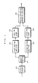
- FIG. 1 is a block diagram showing the structure of an FM modulator according to a first embodiment of the present invention.
- the FM modulator of the present embodiment includes a signal source 100, a branch portion 101, a first frequency modulation laser (hereinafter referred to as a first FM laser) 104, a second frequency modulation laser (hereinafter referred to as a second FM laser ) 105, and an optical-electrical converting portion 106.
- the FM modulator includes first and second driving amplifiers 102 and 103.
- the signal source 100 outputs an electrical signal which is an original signal for FM modulation.
- the branch portion 101 branches the electrical signal outputted from the signal source 100 into a phase-uninverted signal (in-phase signal) and a phase-inverted signal (opposite phase signal) and outputs each of these signals.
- the first and second driving amplifiers 102 and 103 are inserted as required between the branch portion 101 and the first FM laser 104 and between the branch portion 101 and the second FM laser 105, respectively, when the magnitude of the in-phase signal and the opposite phase signal outputted from the branch portion 101 is not sufficient with respect to the required frequency deviation of the first or the second FM lasers 104 and 105, and the like.
- the first and second driving amplifiers 102 and 103 amplify the in-phase signal and the opposite phase signal outputted from the branch portion 101, and then outputs these signals to the first and second FM lasers 104 and 105, respectively.
- the first and second FM lasers 104 and 105 which are typically structured of a semiconductor laser, oscillate light having a constant wavelength under the condition that an injection current is constant.
- the injection current is amplitude-modulated by the electrical signal
- the outputted light is modulated in its oscillation wavelength (optical frequency) as well as in intensity, and the lasers output an optical frequency-modulated signal.
- the first FM laser 104 outputs an optical frequency-modulated signal subjected to modulation with the above in-phase signal and having a center wavelength ⁇ 1 (refer to FIG.
- the second FM laser 105 outputs an optical frequency-modulating signal subjected to modulation by the above opposite phase signal and having a center wavelength ⁇ 2 (refer to FIG. 2b: hereinafter referred to as a second optical signal).
- polarities of frequency deviation in the first and second optical signals have an opposite phase relationship each other, and when the first optical signal is deviated to a high frequency side, the second optical signal is deviated to a low frequency side (as shown by arrows in FIGS. 2a and 2b). On the contrary, when the first optical signal is deviated to a low frequency side, the second optical signal is deviated to a high frequency side.
- the first and second optical signals are combined and then subjected to optical heterodyne detection by a square-law detection characteristic of the optical-electrical converting portion 106.
- the optical-electrical converting portion 106 outputs a wide-band FM signal which is a beat (difference) signal between two optical signals (refer to FIG. 2c).
- the frequency deviation of the wide-band FM signal is the sum of frequency deviation of the first and second optical signals.
- both of the first and second FM lasers are subjected to modulation by electrical signals which have an opposite phase relationship each other, and it is thereby possible to expand the frequency deviation of the outputted signal and thus greatly improve the CNR performance.
- FIG. 3 is a block diagram showing the structure of an FM modulator according to the second embodiment of the present invention.
- the FM modulator of the present embodiment includes, in addition to the structure in FIG. 1, an amplitude adjusting portion 207.
- the amplitude adjusting portion 207 adjusts a signal amplitude level of the in-phase signal outputted from the branch portion 101 to equate frequency deviation of the first and second optical signals. The same effect can be obtained when the amplitude adjusting portion 207 is inserted between the first driving amplifier 102 and the first FM laser 104.
- the amplitude adjusting portion 207 may be inserted between the branch portion 101 and the second FM laser 105 to have the structure for adjusting the amplitude of the opposite phase signal or to have the structure for adjusting the amplitudes of both of the in-phase signal and the opposite phase signal.
- FIG. 4 is a block diagram showing the structure of an FM modulator according to the third embodiment of the present invention.
- the FM modulator of the present embodiment includes, in addition to the structure in FIG. 1, a delay adjusting portion 308.
- the delay adjusting portion 308 adds appropriate propagation delay to the in-phase signal outputted from the branch portion 101 to equate propagation delay with which the in-phase signal outputted from the branch portion 101 reaches through the first FM laser 104 the optical-electrical converting portion 106 and propagation delay with which the opposite phase signal outputted from the branch portion 101 reaches through the second FM laser 105 the optical-electrical converting portion 106.
- the delay adjusting portion 308 is inserted between the first driving amplifier 102 and the first FM laser 104 or between the first FM laser 104 and the optical-electrical converting portion 106. Further, the delay adjusting portion 308 may be inserted between the branch portion 101 and the second FM laser 105 or between the second FM laser 105 and the optical-electrical converting portion 106 to have the structure for adjusting the propagation delay of the opposite phase signal or to have the structure for adjusting the propagation delay of both of the in-phase signal and the opposite phase signal.
- FIG. 5 is a block diagram showing the structure of an FM modulator according to a fourth embodiment of the present invention.
- the FM modulator of the present embodiment includes, in addition to the structure in FIG. 1, a level adjusting portion 409.
- the level adjusting portion 409 adjusts power of the first optical signal outputted from the first FM laser to equate the magnitude of a first IM-DD component by the first optical signal outputted from the optical-electrical converting portion 106 and the magnitude of a second IM-DD component by the second optical signal outputted from the optical-electrical converting portion 106.
- the level adjusting portion 409 may be inserted between the branch portion 101 and the first FM laser 104.
- the level adjusting portion 409 may be inserted between the branch portion 101 and the second FM laser 105 or between the second FM laser 105 and the optical-electrical converting portion 106 to have the structure for adjusting power of the opposite phase signal or to have the structure for adjusting power of both of the in-phase signal and the opposite phase signal.
- the level adjusting portion 409 By appropriately setting a bias current of each semiconductor laser used as the first and second FM lasers 104 and 105 and received light power of the first and second optical signals into the optical-electrical converting portion 106, it is possible to use the level adjusting portion 409 also as the amplitude adjusting portion 207 described in the second embodiment.
- FIG. 6 is a block diagram showing the structure of an FM modulator according to a fifth embodiment of the present invention.
- the FM modulator of the present invention includes, in place of the first and second FM lasers 104 and 105, a first laser light source 510, a first optical phase modulating portion 504, a second laser light source 511, and a second optical phase modulating portion 505.
- the FM modulator includes the amplitude adjusting portion 207 and the delay adjusting portion 308.
- the structure of the present embodiment is basically the same as that of the above described first (second or third) embodiment, but as a method for converting an electrical signal into an optical signal, an "external modulating method" is taken, which is different from the first embodiment (on the other hand, as in the first embodiment, a method for converting an electrical signal into an optical signal by modulating an injection current of a light source is called a "direct modulating method").
- frequency modulation and phase modulation can be thought to have the same meaning, and thus the present embodiment has the structure in which an optical phase-modulated signal is generated as the first and second optical signals.
- the first optical phase modulating portion 504 is provided with unmodulated light from the first light source 510, and converts the in-phase signal outputted from the branch portion 101 into a first optical signal which is an optical phase-modulated signal and then outputs the resultant signal
- the second optical phase modulating portion 505 is provided with unmodulated light from the second light source 511, and converts the opposite phase signal outputted from the branch portion 101 into a second optical signal which is an optical phase-modulated signal and then outputs the resultant signal.
- These two optical signals are then subjected to optical heterodyne detection in the optical-electrical converting portion 106 to generate a wide-band FM signal.
- the amplitude adjusting portion 207 and the delay adjusting portion 308 are inserted in an appropriate position as required, thereby equating frequency (phase) deviation in the first and second optical signals and equating propagation delay in which the in-phase signal and the opposite phase signal reach from the branch portion 101 to the optical-electrical converting portion 106.
Landscapes
- Optical Communication System (AREA)
- Optical Modulation, Optical Deflection, Nonlinear Optics, Optical Demodulation, Optical Logic Elements (AREA)
Applications Claiming Priority (2)
| Application Number | Priority Date | Filing Date | Title |
|---|---|---|---|
| JP9232577A JPH1174847A (ja) | 1997-08-28 | 1997-08-28 | Fm変調装置 |
| EP98116185A EP0899867B1 (de) | 1997-08-28 | 1998-08-27 | FM-Modulator |
Related Parent Applications (1)
| Application Number | Title | Priority Date | Filing Date |
|---|---|---|---|
| EP98116185A Division EP0899867B1 (de) | 1997-08-28 | 1998-08-27 | FM-Modulator |
Publications (3)
| Publication Number | Publication Date |
|---|---|
| EP1615334A2 true EP1615334A2 (de) | 2006-01-11 |
| EP1615334A3 EP1615334A3 (de) | 2009-02-25 |
| EP1615334B1 EP1615334B1 (de) | 2010-01-06 |
Family
ID=16941540
Family Applications (2)
| Application Number | Title | Priority Date | Filing Date |
|---|---|---|---|
| EP05017363A Expired - Lifetime EP1615334B1 (de) | 1997-08-28 | 1998-08-27 | FM-Modulator |
| EP98116185A Expired - Lifetime EP0899867B1 (de) | 1997-08-28 | 1998-08-27 | FM-Modulator |
Family Applications After (1)
| Application Number | Title | Priority Date | Filing Date |
|---|---|---|---|
| EP98116185A Expired - Lifetime EP0899867B1 (de) | 1997-08-28 | 1998-08-27 | FM-Modulator |
Country Status (4)
| Country | Link |
|---|---|
| US (3) | US6512621B1 (de) |
| EP (2) | EP1615334B1 (de) |
| JP (1) | JPH1174847A (de) |
| DE (2) | DE69841441D1 (de) |
Families Citing this family (12)
| Publication number | Priority date | Publication date | Assignee | Title |
|---|---|---|---|---|
| JPH1174847A (ja) * | 1997-08-28 | 1999-03-16 | Matsushita Electric Ind Co Ltd | Fm変調装置 |
| JPH11261494A (ja) * | 1998-03-09 | 1999-09-24 | Fujitsu Ltd | 光ヘテロダイン型fm変調器 |
| US6643470B1 (en) * | 1999-10-01 | 2003-11-04 | Matsushita Electric Industrial Co., Ltd. | FM signal converter, FM signal optical transmitter and FM signal optical receiver |
| US6941078B1 (en) * | 2001-05-10 | 2005-09-06 | Fujitsu Limited | Method and system for communicating a clock signal over an optical link |
| US7295584B2 (en) | 2001-12-17 | 2007-11-13 | Peleton Photonic Systems | System and method for generating multi-wavelength laser source using highly nonlinear fiber |
| US6826207B2 (en) | 2001-12-17 | 2004-11-30 | Peleton Photonic Systems Inc. | Multi-wavelength laser source based on two optical laser beat signal and method |
| GB2415309A (en) * | 2004-06-18 | 2005-12-21 | Univ Kent Canterbury | Electro-magnetic terahertz transmission/reception system |
| JP3955292B2 (ja) | 2004-07-30 | 2007-08-08 | 松下電器産業株式会社 | Fm変調器 |
| KR100640006B1 (ko) * | 2005-10-14 | 2006-11-01 | 한국전자통신연구원 | 광학적 클럭 신호 추출 장치 및 방법 |
| JP4828447B2 (ja) * | 2007-02-08 | 2011-11-30 | 日本電信電話株式会社 | 周波数変調器 |
| JP2010062619A (ja) * | 2008-09-01 | 2010-03-18 | Nippon Telegr & Teleph Corp <Ntt> | 周波数変調信号発生方法及び発生装置 |
| WO2022172381A1 (ja) * | 2021-02-10 | 2022-08-18 | 日本電信電話株式会社 | 光送信装置、光送信方法及び光伝送システム |
Family Cites Families (19)
| Publication number | Priority date | Publication date | Assignee | Title |
|---|---|---|---|---|
| JPH0239131A (ja) | 1988-07-29 | 1990-02-08 | Hitachi Ltd | 周波数間隔安定化方法、光ヘテロダイン又は光ホモダイン通信方法 |
| US5252930A (en) * | 1989-09-07 | 1993-10-12 | Ortel Corporation | Predistorter for linearization of electronic and optical signals |
| JPH03209927A (ja) * | 1990-01-12 | 1991-09-12 | Fujitsu Ltd | ヘテロダイン送信機 |
| JPH047882A (ja) * | 1990-04-25 | 1992-01-13 | Mitsubishi Electric Corp | 半導体レーザ装置 |
| US5212579A (en) | 1991-03-11 | 1993-05-18 | General Instrument Corporation | Method and apparatus for communicating amplitude modulated signals over an optical communication path |
| JPH04346525A (ja) | 1991-05-24 | 1992-12-02 | Matsushita Electric Ind Co Ltd | コヒーレント光伝送装置 |
| GB2264834A (en) | 1992-02-25 | 1993-09-08 | Northern Telecom Ltd | Optical transmission system |
| US5396216A (en) * | 1993-07-28 | 1995-03-07 | Morgan; Lonnie | Vehicle theft deterrent system including hood locking means |
| US5523158A (en) * | 1994-07-29 | 1996-06-04 | Saint Gobain/Norton Industrial Ceramics Corp. | Brazing of diamond film to tungsten carbide |
| US5526158A (en) | 1994-12-22 | 1996-06-11 | Trw Inc. | Low-bias heterodyne fiber-optic communication link |
| JPH0946300A (ja) | 1995-07-28 | 1997-02-14 | Furukawa Electric Co Ltd:The | 光通信方法 |
| US5699179A (en) | 1996-02-23 | 1997-12-16 | General Instrument Corporation Of Delaware | Cancellation of distortion components in a fiber optic link with feed-forward linearization |
| DE69624680T2 (de) * | 1996-04-05 | 2003-09-18 | Nippon Telegraph And Telephone Corp., Tokio/Tokyo | AM/FM Umsetzer und Lichtwellensignalübertragungssystem |
| JPH1056424A (ja) | 1996-08-13 | 1998-02-24 | Matsushita Electric Ind Co Ltd | 広帯域fm変調装置 |
| JP3482088B2 (ja) * | 1996-12-05 | 2003-12-22 | 松下電器産業株式会社 | 周波数変調装置 |
| JP3444519B2 (ja) * | 1997-05-19 | 2003-09-08 | 松下電器産業株式会社 | Fm変調装置 |
| JPH1174847A (ja) * | 1997-08-28 | 1999-03-16 | Matsushita Electric Ind Co Ltd | Fm変調装置 |
| JP3097618B2 (ja) | 1997-09-30 | 2000-10-10 | 日本電気株式会社 | Fm変調器 |
| US6542621B1 (en) * | 1998-08-31 | 2003-04-01 | Texas Instruments Incorporated | Method of dealing with occlusion when tracking multiple objects and people in video sequences |
-
1997
- 1997-08-28 JP JP9232577A patent/JPH1174847A/ja active Pending
-
1998
- 1998-08-26 US US09/140,658 patent/US6512621B1/en not_active Expired - Lifetime
- 1998-08-27 DE DE69841441T patent/DE69841441D1/de not_active Expired - Lifetime
- 1998-08-27 EP EP05017363A patent/EP1615334B1/de not_active Expired - Lifetime
- 1998-08-27 DE DE69832560T patent/DE69832560T2/de not_active Expired - Lifetime
- 1998-08-27 EP EP98116185A patent/EP0899867B1/de not_active Expired - Lifetime
-
2002
- 2002-11-15 US US10/294,759 patent/US6687465B2/en not_active Expired - Fee Related
-
2003
- 2003-12-15 US US10/734,186 patent/US6909855B2/en not_active Expired - Fee Related
Also Published As
| Publication number | Publication date |
|---|---|
| EP1615334B1 (de) | 2010-01-06 |
| US6687465B2 (en) | 2004-02-03 |
| US20030067661A1 (en) | 2003-04-10 |
| EP0899867A2 (de) | 1999-03-03 |
| JPH1174847A (ja) | 1999-03-16 |
| DE69841441D1 (de) | 2010-02-25 |
| US6512621B1 (en) | 2003-01-28 |
| EP0899867B1 (de) | 2005-11-30 |
| US20040126121A1 (en) | 2004-07-01 |
| DE69832560D1 (de) | 2006-01-05 |
| DE69832560T2 (de) | 2006-08-24 |
| EP0899867A3 (de) | 1999-12-08 |
| US6909855B2 (en) | 2005-06-21 |
| EP1615334A3 (de) | 2009-02-25 |
Similar Documents
| Publication | Publication Date | Title |
|---|---|---|
| JP4178617B2 (ja) | 光伝送システム、光送信装置及び光送信方法 | |
| US6211996B1 (en) | Angle modulator | |
| US6556327B1 (en) | Signal converter, optical transmitter and optical fiber transmission system | |
| US20020005971A1 (en) | Radio-frequency transmitter with function of distortion compensation | |
| EP1615334B1 (de) | FM-Modulator | |
| US20020171894A1 (en) | Optical linearizer for fiber communications | |
| US5547274A (en) | Modulated light source with a linear transfer function | |
| US20010030791A1 (en) | Optical transmitter | |
| JP4577945B2 (ja) | 角度変調装置 | |
| US7269354B1 (en) | Superheterodyne photonic receiver using non-serial frequency translation | |
| US6819877B1 (en) | Optical links | |
| JPH11145535A (ja) | 信号変換器、光送信器および光ファイバ伝送装置 | |
| Woo et al. | Feedforward compensation of laser frequency and phase noise for photonics-based sub-THz generation | |
| US5245461A (en) | Analog optical FM receiver | |
| US20080292326A1 (en) | Optical Voltage Controlled Oscillator for an Optical Phase Locked Loop | |
| US6512619B1 (en) | Frequency modulation apparatus | |
| JP3444519B2 (ja) | Fm変調装置 | |
| JP4728275B2 (ja) | 光ssb送信装置 | |
| US12407409B2 (en) | Single-sideband reduced-carrier phase-shifting electro-optic modulator | |
| JP3575653B2 (ja) | 超高速同期パルス光源 | |
| JP4219519B2 (ja) | 周波数変調装置 | |
| JPH1127212A (ja) | 広帯域光周波数変調器 | |
| US5923687A (en) | Bandwidth enhancement and broadband noise reduction in injection-locked semiconductor lasers | |
| JPH0285830A (ja) | コヒーレント光受信方式 | |
| JPH1013354A (ja) | 多チャンネル信号変復調装置 |
Legal Events
| Date | Code | Title | Description |
|---|---|---|---|
| PUAI | Public reference made under article 153(3) epc to a published international application that has entered the european phase |
Free format text: ORIGINAL CODE: 0009012 |
|
| AC | Divisional application: reference to earlier application |
Ref document number: 0899867 Country of ref document: EP Kind code of ref document: P |
|
| AK | Designated contracting states |
Kind code of ref document: A2 Designated state(s): DE FR GB |
|
| AX | Request for extension of the european patent |
Extension state: AL LT LV MK RO SI |
|
| RAP1 | Party data changed (applicant data changed or rights of an application transferred) |
Owner name: PANASONIC CORPORATION |
|
| PUAL | Search report despatched |
Free format text: ORIGINAL CODE: 0009013 |
|
| AK | Designated contracting states |
Kind code of ref document: A3 Designated state(s): DE FR GB |
|
| AX | Request for extension of the european patent |
Extension state: AL LT LV MK RO SI |
|
| 17P | Request for examination filed |
Effective date: 20090327 |
|
| 17Q | First examination report despatched |
Effective date: 20090427 |
|
| GRAP | Despatch of communication of intention to grant a patent |
Free format text: ORIGINAL CODE: EPIDOSNIGR1 |
|
| AKX | Designation fees paid |
Designated state(s): DE FR GB |
|
| GRAS | Grant fee paid |
Free format text: ORIGINAL CODE: EPIDOSNIGR3 |
|
| GRAA | (expected) grant |
Free format text: ORIGINAL CODE: 0009210 |
|
| AC | Divisional application: reference to earlier application |
Ref document number: 0899867 Country of ref document: EP Kind code of ref document: P |
|
| AK | Designated contracting states |
Kind code of ref document: B1 Designated state(s): DE FR GB |
|
| REG | Reference to a national code |
Ref country code: GB Ref legal event code: FG4D |
|
| REF | Corresponds to: |
Ref document number: 69841441 Country of ref document: DE Date of ref document: 20100225 Kind code of ref document: P |
|
| PLBE | No opposition filed within time limit |
Free format text: ORIGINAL CODE: 0009261 |
|
| STAA | Information on the status of an ep patent application or granted ep patent |
Free format text: STATUS: NO OPPOSITION FILED WITHIN TIME LIMIT |
|
| 26N | No opposition filed |
Effective date: 20101007 |
|
| PGFP | Annual fee paid to national office [announced via postgrant information from national office to epo] |
Ref country code: DE Payment date: 20110824 Year of fee payment: 14 Ref country code: FR Payment date: 20110818 Year of fee payment: 14 Ref country code: GB Payment date: 20110824 Year of fee payment: 14 |
|
| GBPC | Gb: european patent ceased through non-payment of renewal fee |
Effective date: 20120827 |
|
| REG | Reference to a national code |
Ref country code: FR Ref legal event code: ST Effective date: 20130430 |
|
| PG25 | Lapsed in a contracting state [announced via postgrant information from national office to epo] |
Ref country code: GB Free format text: LAPSE BECAUSE OF NON-PAYMENT OF DUE FEES Effective date: 20120827 Ref country code: DE Free format text: LAPSE BECAUSE OF NON-PAYMENT OF DUE FEES Effective date: 20130301 |
|
| PG25 | Lapsed in a contracting state [announced via postgrant information from national office to epo] |
Ref country code: FR Free format text: LAPSE BECAUSE OF NON-PAYMENT OF DUE FEES Effective date: 20120831 |
|
| REG | Reference to a national code |
Ref country code: DE Ref legal event code: R119 Ref document number: 69841441 Country of ref document: DE Effective date: 20130301 |