EP1653786A2 - Stromresonanzumrichter und Verfahren zur Leistungssteuerung - Google Patents
Stromresonanzumrichter und Verfahren zur Leistungssteuerung Download PDFInfo
- Publication number
- EP1653786A2 EP1653786A2 EP05256722A EP05256722A EP1653786A2 EP 1653786 A2 EP1653786 A2 EP 1653786A2 EP 05256722 A EP05256722 A EP 05256722A EP 05256722 A EP05256722 A EP 05256722A EP 1653786 A2 EP1653786 A2 EP 1653786A2
- Authority
- EP
- European Patent Office
- Prior art keywords
- current
- transformer
- circuit
- inverter circuit
- resonance type
- Prior art date
- Legal status (The legal status is an assumption and is not a legal conclusion. Google has not performed a legal analysis and makes no representation as to the accuracy of the status listed.)
- Withdrawn
Links
- 238000000034 method Methods 0.000 title claims abstract description 155
- 238000004804 winding Methods 0.000 claims abstract description 95
- 230000010355 oscillation Effects 0.000 claims abstract description 38
- 239000003990 capacitor Substances 0.000 claims abstract description 17
- 230000003213 activating effect Effects 0.000 claims description 6
- 230000003071 parasitic effect Effects 0.000 claims description 6
- 230000001360 synchronised effect Effects 0.000 claims description 6
- 238000013016 damping Methods 0.000 claims description 3
- 238000010586 diagram Methods 0.000 description 54
- 238000006243 chemical reaction Methods 0.000 description 23
- 230000008859 change Effects 0.000 description 8
- 230000000694 effects Effects 0.000 description 7
- 230000006872 improvement Effects 0.000 description 7
- 230000008878 coupling Effects 0.000 description 6
- 238000010168 coupling process Methods 0.000 description 6
- 238000005859 coupling reaction Methods 0.000 description 6
- 230000004907 flux Effects 0.000 description 5
- 230000001172 regenerating effect Effects 0.000 description 5
- RYGMFSIKBFXOCR-UHFFFAOYSA-N Copper Chemical compound [Cu] RYGMFSIKBFXOCR-UHFFFAOYSA-N 0.000 description 3
- 239000002131 composite material Substances 0.000 description 3
- 229910052802 copper Inorganic materials 0.000 description 3
- 239000010949 copper Substances 0.000 description 3
- 230000001419 dependent effect Effects 0.000 description 2
- 238000002474 experimental method Methods 0.000 description 2
- 238000009499 grossing Methods 0.000 description 2
- 239000004973 liquid crystal related substance Substances 0.000 description 2
- 238000012546 transfer Methods 0.000 description 2
- 238000013459 approach Methods 0.000 description 1
- 230000000052 comparative effect Effects 0.000 description 1
- 230000010485 coping Effects 0.000 description 1
- 230000007423 decrease Effects 0.000 description 1
- 238000011161 development Methods 0.000 description 1
- 239000006185 dispersion Substances 0.000 description 1
- 238000004519 manufacturing process Methods 0.000 description 1
- 229910052754 neon Inorganic materials 0.000 description 1
- GKAOGPIIYCISHV-UHFFFAOYSA-N neon atom Chemical compound [Ne] GKAOGPIIYCISHV-UHFFFAOYSA-N 0.000 description 1
- 230000002093 peripheral effect Effects 0.000 description 1
- 230000009467 reduction Effects 0.000 description 1
- 238000009774 resonance method Methods 0.000 description 1
- 229920006395 saturated elastomer Polymers 0.000 description 1
- 238000004088 simulation Methods 0.000 description 1
- 230000006641 stabilisation Effects 0.000 description 1
- 238000011105 stabilization Methods 0.000 description 1
- 230000009466 transformation Effects 0.000 description 1
Images











Classifications
-
- H—ELECTRICITY
- H05—ELECTRIC TECHNIQUES NOT OTHERWISE PROVIDED FOR
- H05B—ELECTRIC HEATING; ELECTRIC LIGHT SOURCES NOT OTHERWISE PROVIDED FOR; CIRCUIT ARRANGEMENTS FOR ELECTRIC LIGHT SOURCES, IN GENERAL
- H05B41/00—Circuit arrangements or apparatus for igniting or operating discharge lamps
- H05B41/14—Circuit arrangements
- H05B41/26—Circuit arrangements in which the lamp is fed by power derived from DC by means of a converter, e.g. by high-voltage DC
- H05B41/28—Circuit arrangements in which the lamp is fed by power derived from DC by means of a converter, e.g. by high-voltage DC using static converters
- H05B41/282—Circuit arrangements in which the lamp is fed by power derived from DC by means of a converter, e.g. by high-voltage DC using static converters with semiconductor devices
-
- H—ELECTRICITY
- H02—GENERATION; CONVERSION OR DISTRIBUTION OF ELECTRIC POWER
- H02M—APPARATUS FOR CONVERSION BETWEEN AC AND AC, BETWEEN AC AND DC, OR BETWEEN DC AND DC, AND FOR USE WITH MAINS OR SIMILAR POWER SUPPLY SYSTEMS; CONVERSION OF DC OR AC INPUT POWER INTO SURGE OUTPUT POWER; CONTROL OR REGULATION THEREOF
- H02M7/00—Conversion of AC power input into DC power output; Conversion of DC power input into AC power output
- H02M7/42—Conversion of DC power input into AC power output without possibility of reversal
- H02M7/44—Conversion of DC power input into AC power output without possibility of reversal by static converters
- H02M7/48—Conversion of DC power input into AC power output without possibility of reversal by static converters using discharge tubes with control electrode or semiconductor devices with control electrode
- H02M7/505—Conversion of DC power input into AC power output without possibility of reversal by static converters using discharge tubes with control electrode or semiconductor devices with control electrode using devices of a thyratron or thyristor type requiring extinguishing means
- H02M7/51—Conversion of DC power input into AC power output without possibility of reversal by static converters using discharge tubes with control electrode or semiconductor devices with control electrode using devices of a thyratron or thyristor type requiring extinguishing means using discharge tubes only
-
- H—ELECTRICITY
- H02—GENERATION; CONVERSION OR DISTRIBUTION OF ELECTRIC POWER
- H02M—APPARATUS FOR CONVERSION BETWEEN AC AND AC, BETWEEN AC AND DC, OR BETWEEN DC AND DC, AND FOR USE WITH MAINS OR SIMILAR POWER SUPPLY SYSTEMS; CONVERSION OF DC OR AC INPUT POWER INTO SURGE OUTPUT POWER; CONTROL OR REGULATION THEREOF
- H02M7/00—Conversion of AC power input into DC power output; Conversion of DC power input into AC power output
- H02M7/42—Conversion of DC power input into AC power output without possibility of reversal
- H02M7/44—Conversion of DC power input into AC power output without possibility of reversal by static converters
- H02M7/48—Conversion of DC power input into AC power output without possibility of reversal by static converters using discharge tubes with control electrode or semiconductor devices with control electrode
Definitions
- the present invention relates to a dependent invention of Japanese Patent No. 2733817 (U.S. Patent No. 5,495,405) relating to the invention of the inventor of this application or contents of the technical significance of the invention.
- the present invention relates to an inverter circuit for a light source, having a capacitive characteristics, such as a Cold Cathode Fluorescent Lamp (CCFL), an External Electrode Fluorescent Lamp (EEFL), or a neon lamp.
- CCFL Cold Cathode Fluorescent Lamp
- EEFL External Electrode Fluorescent Lamp
- a collector resonance type circuit As for the inverter circuit for a cold cathode fluorescent lamp, a collector resonance type circuit (refer to Fig. 17) has been widely used.
- This collector resonance type circuit is referred as another name to as “a Royer circuit” in some cases.
- the proper definition of the Royer circuit is such that the inversion of a switching operation is performed in a state in which a transformer is saturated.
- the inverter circuit which performs the inversion operation by utilizing the resonance on the collector side is desirably referred to as "a collector resonance type circuit” or "a collector resonance type Royer circuit” in distinction from the Royer circuit.
- the initial inverter circuit for a cold cathode fluorescent lamp did not utilize the resonance method of a secondary side circuit at all, and the so-called closed magnetic circuit type transformer having a small leakage inductance was used in a step-up transformer.
- the so-called closed magnetic circuit type transformer method a transformer having a small leakage inductance in terms of recognition of a person skilled in the art.
- the leakage inductance of the step-up transformer in the inverter circuit was recognized such that it reduced an output voltage on a secondary side of a transformer and was not preferable, and thus was desirably as small as possible.
- a resonance frequency of the secondary side circuit of the transformer in the background of the times was judged to have no connection with an operating frequency of the inverter circuit.
- a ballast capacitor Cb is essential for stabilization of a lamp current.
- an inverter circuit shown in Fig. 18 is known.
- this inverter circuit is one disclosed in Japanese Unexamined Patent Publication No. Hei 7-211472, and has come into wide use as the so-called three-time resonance circuit in which as shown in Fig. 19, the resonance frequency of the secondary side circuit is three times as high as an oscillation frequency of a primary side circuit.
- a step-up transformer in which a leakage inductance value is increased to some degree is suitable for one used in this case.
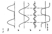
- the signal having the oscillation frequency of the inverter circuit and the third-order harmonics are composed with each other to generate a signal having a trapezoid waveform.
- the current which is actually caused to flow through the cold cathode fluorescent lamp of the three-time resonance circuit shows a waveform as shown in Fig. 21.
- step-up transformer There is confusion in the name of the step-up transformer in this case. There is controversy as to whether or not the step-up transformer may be referred to as "the so-called closed magnetic circuit type transformer" which is said among those skilled in the art. Thus, the definition of the name of the step-up transformer becomes vague. There is a problem as to how a state is described in which the leakage of the magnetic flux is much though the magnetic path structure is closed. A problem still exists such that those terms are not the special technical term each in which the state as described above is supposed.
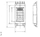
- the shape of the transformer which is actually used in the so-called three-time resonance is flat as shown in Fig. 22.
- the leakage of the magnetic flux is considerably more than that of the conventional one. That is, that transformer has a large leakage inductance value.
- this technical idea is such that the leakage inductance value of the step-up transformer is increased to some degree, whereby a resonance circuit is structured by using a leakage inductance (Le in Fig. 18) and a capacitance component obtained on the secondary side of the step-up transformer, and a resonance frequency of the resonance circuit is set to a frequency three times as high as the operating frequency of the inverter circuit in order to generate a third-order harmonics in the secondary side circuit (refer to Fig. 19), thereby obtaining a lamp current waveform having a trapezoid shape (refer to Fig. 20D).
- a ballast capacitor C2 in this case though being a ballast capacitor, functions as a part of a resonance capacitor.
- the present invention began to be widely implemented in about 1996, and thus has greatly contributed to the miniaturization and high efficiency promotion of the inverter circuit used in a note type personal computer.
- the invention concerned is the invention such that the operating frequency of the inverter circuit and the resonance frequency of the secondary side circuit are made nearly agree with each other.
- the leakage inductance value of the step-up transformer in the three-time resonance is further increased, and at the same time the capacitance component of the secondary side circuit is increased, thereby realizing the invention concerned.
- This technique utilizes such an effect that when the inverter circuit operates in the vicinity of the resonance frequency of the secondary side circuit, an exciting current which is caused to flow through a primary winding of the step-up transformer becomes less.
- a power factor when viewed from the primary winding side is enhanced, and a copper loss of the step-up transformer decreases.
- Fig. 23 is a graphical representation explaining the technique for improving the power factor when viewed from the driving method side.
- an axis of abscissa represents a frequency
- â represents a phase difference between a voltage phase and a current phase in a primary winding of a step-up transformer.
- Fig. 23 explains that the power factor is improved as è becomes nearer zero.
- the zero current switching method is one of power controlling method of the inverter circuit, and examples of the zero current switching type circuit as shown in Figs. 24 and 30 are disclosed as typical ones in U.S. Patent No. 6114814-B1 and Japanese Unexamined Patent Publication No. Sho 59-032370.
- the inventor of the present invention also discloses as the same technique as that described above in Japanese Unexamined Patent Publication No. Hei 8-288080 (refer to Fig. 29). This technique will be described based on U.S. Patent No. 6114814-B1 as follows.
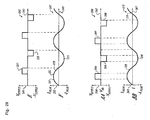
- Figs. A to D of Fig. 25 correspond to Figs. 11A to 11D shown in U.S. Patent No. 6114814-B1, respectively
- Figs. E to F and AA and BB of Fig. 26 correspond to Figs. 11E and 11F
- Figs. 12A and 12B shown in U.S. Patent No. 6114814-B1, respectively.
- Figs. 11A to 11D and Figs. 12A and 12B show waveform diagrams explaining an operation of the zero current switching type circuit of the invention concerned.
- Figs. 11A and 11B in U.S. Patent No. 6114814-B1 show a state in which no power control is performed
- Figs. 11C and 11D in U.S. Patent No. 6114814-B1 show a state in which the power control is performed
- Figs. 11E and 11F in U.S. Patent No. 6114814-B1 show a case where the zero current switching operation is intended to be performed in a state in which a phase of an effective voltage value leads a phase of an effective current value.
- FIG. 26 diagrams as shown in Fig. 26 are shown as Figs. 12A and 12B in U.S. Patent No. 6114814-B1, and such Figs. 12A and 12B show an example of control in a case of no zero current switching operation.
- Fig. 11A in U.S. Patent No. 6114814-B1 shows a voltage applied to a primary winding of a transformer when a driving power is the maximum
- Fig. 11B in U.S. Patent No. 6114814-B1 shows a current which is caused to flow through the primary winding of the transformer in that case.
- the zero current switching method in the inverter circuit for a cold cathode fluorescent lamp serves to detect timing at which the current value becomes zero to turn ON a switching element.
- the driving power is the maximum, i.e., when a flow angle is set to 100% and thus no power control is performed, there is necessarily no phase difference between the phase of the effective voltage value and the phase of the effective current value which is given to the primary winding. That is, this method that the power factor is satisfactory.
- Fig. 11C in U.S. Patent No. 6114814-B1 shows a voltage applied to the primary winding of the transformer when the flow angle is made small in order to control the driving power.
- Fig. 11D in U.S. Patent No. 6114814-B1 shows a current which is caused to flow through the primary winding in this case.
- a switching transistor is turned ON at timing at which the current value becomes zero.
- turn-OFF of the switching transistor is not caused at the timing at which the current value becomes zero.
- the power factor in this case is not satisfactory.
- Fig. AA of Fig. 26 shows a case where the power control is performed with the flow angle being similarly limited, the control is performed such that the phase of the effective value of the voltage in the primary winding and the phase of the effective value of the current caused to flow through the primary winding become equal to each other under a condition in which the zero current switching method is disregarded.
- the power factor when viewed from the primary winding side of the transformer is really satisfactory, and thus the exothermic quantity of step-up transformer is less.
- this technique is not related to zero current switching method.
- the zero current switching method is in consistent with the technical idea for providing the high efficiency for the inverter circuit.
- the zero current switching method is excluded in the states as shown in Figs. 12A and 12B in U.S. Patent No. 6114814-B1 because of the unsatisfactory conversion efficiency of the inverter circuit.
- the phase difference between the phase of the voltage applied to the primary winding of the step-up transformer and the phase of the current caused to flow through the primary winding thereof necessarily disappears.
- the power factor of the step-up transformer is improved, the current caused to flow through the primary winding is reduced, and the current caused to flow through the switching transistor becomes the minimum.
- the exothermic quantity of primary winding of the step-up transformer and the exothermic quantity of switching transistor are reduced, so that the efficiency of the inverter circuit is improved. It seems that this fact is misidentified as that the high efficiency is provided by the zero current switching method.
- the state as shown in 11A and 11B in U.S. Patent No. 6114814-B1 corresponds to a case where no power control is performed.
- An operating state in this case becomes equivalent to an operating state of the general current resonance type inverter circuit. That is, it is found out that the high-efficiency inverter circuit is not provided by the zero current switching method, but really provided by the conventional current resonance type method.
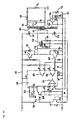
- the current resonance type inverter circuit is known as one for a cold cathode fluorescent lamp, and for example, a circuit as shown in FIG. 27 is generally used as the current resonance type inverter circuit.
- Such a current resonance type circuit has no dimming method in a case where only a structure of a basic circuit is adopted. Then, when the dimming is performed in the current resonance type inverter circuit, the dimming is performed by using a DC-DC converter circuit is provided in a preceding stage of the current resonance type inverter circuit in order to perform the dimming.
- FIG. 28 shows an example of a dimming circuit in an inverter circuit for a cold cathode fluorescent lamp in which the conventional current resonance type circuit is combined with a DC-DC converter circuit provided in a preceding stage thereof.
- switching method Qs, a choke coil Lc, a fly-wheel diode Ds, and smoothing capacitor Cv constitute the DC-DC converter circuit.
- Fig. 29 shows a dimming circuit which the inventor of the present invention disclosed in JAPANESE UNEXAMINED PATENT PUBLICATION 8-288080 A.
- timer circuits 10 and 11 detect a zero current, and after a lapse of a predetermined period of time, a frequency controlling circuit 12 turns OFF switching elements 2 and 3.
- Each of the timer circuits 10 and 11 is structured in the form of an RS flip-flop, and set with the zero current and reset after a lapse of a given period of time.
- This dimming circuit is one for performing the dimming by utilizing a method of turning OFF switching method after a lapse of a given period of time after detecting the zero current to turn ON the switching method.
- Fig. 30 is a circuit diagram shown in Fig. 9 of U. S. Patent No. 6114814-B1.
- an RS flip-flop 172 is set by a zero current, and reset after a lapse of a given period of time.
- Each of the techniques disclosed in U.S. Patent No. 6114814-B1 and Japanese Unexamined Patent Publication No. Hei 8-288080 is such that at the same time that the zero current is detected to turn ON the switching method, the RS flip-flop is set, and reset after a lapse of a given period of time, thereby turning OFF the switching method.
- Each of these techniques gives the switching method of the current resonance type circuit the dimming function, and thus has such a feature that a phase of the current laps a phase of the effective voltage during the dimming phase.
- those techniques are established based on the completely same technical idea, and nearly identical in realization method to each other.
- the dimming of the discharge lamp is generally controlled by the DC-DC converter circuit provided in the preceding stage of the collector resonance type circuit.
- the operating frequency of such a DC-DC converter circuit generally has no connection with the oscillation frequency of the inverter circuit.
- the switching timing depends on neither the zero voltage nor the zero current. In spite of this situation, an exothermic quantity of switching method of the DC-DC converter circuit is not so much. Thus, the DC-DC converter circuit does not reduce the conversion efficiency of the overall inverter circuit.
- the reason that the conversion efficiency is low in the conventional inverter circuit is that the conversion efficiency of the collector resonance type circuit is low, and is not that the conversion efficiency of the DC-DC converter circuit is low. This method that the zero current switching method does not necessarily contribute to the improvement in the conversion efficiency of the inverter circuit.
- the waveform of Fig. C of Fig. 25 is adopted in order to perform the power control.
- the power control is performed with the flow angle being limited, as shown in Figs. C and D of Fig. 25, the phase difference between the phase of the effective voltage value and the phase of the current becomes large, the lowering of power factor will increase the current, and the copper loss increases accordingly, so that the thermal loss of primary winding of the transformer increases.
- the exothermic quantity of transistor constituting the switching method increases since the current increases. As a result, the conversion efficiency of the inverter circuit is reduced.
- the factor which most contributes to the improvement in the conversion efficiency of the inverter circuit for a cold cathode fluorescent lamp is not the zero current switching method.
- the effect of improving the power factor of the step-up transformer under the specific condition which is provided by the zero current switching method predominantly contributes to the improvement in the conversion efficiency of the inverter circuit for a cold cathode fluorescent lamp.
- the case under the specific condition corresponds to a case where no flow angle is limited. This is fit for the current resonance type circuit.
- Fig. 31 is a graphical representation in the form of which the relationship between the voltage shown in Fig. C of Fig. 25 and the current shown in Fig. D of Fig. 25 is summarized and which explains a relationship between the voltage and current in the primary winding of the transformer in the zero current switching method, and their phases. That is, Fig. 31 is a graph in a case where the flow angle in Figs. C and D of Fig. 25 when the power control is performed is set to about 25%. In this case, a point a in Fig. 31 represents timing at which the switching method is turned ON, while a point b represents timing at which the switching method is turned OFF.
- a waveform Es is one of the voltage applied to the primary winding of the transformer
- a waveform Er is one of the effective value of the voltage in the primary winding of the transformer
- a waveform Iw is one of the current caused to flow through the primary winding of the transformer.
- Fig. 32 shows this situation in the form of a graph.
- Fig. 32 is a graphical representation which is obtained by calculating how the phase of the effective voltage value and the phase of the current change along with the change in flow angle. This diagram explains that when the flow angle is 25%, the lag angle of the current with respect to the voltage is 67.5 degrees. From this diagram, when the flow angle (duty ratio) is set to 25%, the phase lag of the current with respect to the voltage is obtained as about 67.5 degrees.
- Figs. 33 and 34 are respectively a diagram and a graphical representation which are obtained by examining the power factor.
- Fig. 34 is a graph which represents a relationship among a load current obtained through the primary-side conversion, the exciting current and the current caused to flow through the primary winding when the power factor is examined, and which explains that the much exciting current is caused to flow and a reactive current increases as the lag angle becomes larger.
- Fig. 34 a composite current ratio method 1/cos ⁇ (the reciprocal number of the power factor).
- Fig. 34 shows a relationship between a current lag angle ⁇ as lag of the current phase with respect to the phase of the effective voltage value and 1/cos ⁇ (the reciprocal number of the power factor).
- What times the primary winding current as much as the load current is caused to flow is examined as shown in Fig. 34.
- the current caused to flow through the primary winding when the phase of the current lags the phase of the effective voltage value by 67.5 degrees is 2.61 times as much as that when the phase of the current does not lag the phase of the effective voltage value at all.
- the power factor is very poor, and the exothermic quantity of primary winding increases due to an increase in copper loss.
- the exothermic quantity of transistor constituting the switching method also increases for the same reason.
- the excellent conversion efficiency is obtained in the inverter circuit in a state in which the flow angle is wide, i.e., in a state in which the lag of the phase of the current with respect to the phase of the effective voltage value is small.
- the flow angle is small, the lag of the phase of the current with respect to the phase of the effective voltage value is large, and thus the power factor becomes poor.
- the current caused to flow through the primary winding of the transformer increases, whereby the conversion efficiency of the converter circuit becomes worse.
- the flow angle is narrow, as the lag of the current phase approaches 90 degrees, the reactive current abruptly increases, and the conversion efficiency remarkably becomes worse.
- the evident fact is that the technical idea called the zero current switching is not necessarily essential to the structure of the inverter circuit having the excellent conversion efficiency in a state in which the power control is performed. Far from that, the technical idea called the zero current switching is rather harmful than is not necessarily essential thereto.
- the technical idea called the zero current switching is rather harmful than is not necessarily essential thereto.
- the inverter circuit having the high efficiency when the zero current switching method and the separately excited driving method having the fixed frequency is used, it is possible to structure the inverter circuit having the high efficiency. In this case, however, there is encountered such a problem that there are a large number of constants of the circuit components, and the zero current switching method or the separately excited driving method is expensive.
- the collector resonance type circuit involves such a problem that the efficiency is poor and there is the much calorification, it is inexpensive. From this, the collector resonance type circuit is still firmly supported as the method for reducing the cost. Those problems are an obstacle to the spread of the high-efficiency inverter circuit.
- the present invention has been made in the light of the viewpoint as described above, and it is therefore an object of the present invention to provide a higher-efficiency current resonance type inverter circuit for which the conventional collector resonance type inverter circuit for a discharge lamp is excluded to be replaced with the current resonance type inverter circuit for a discharge lamp, thereby reflecting the technical significance of Japanese Patent No. 2733817 (U.S. Patent No. 5,495,405) therein.
- a current resonance type inverter circuit for a discharge lamp including: a step-up transformer, a primary winding of the step-up transformer having a center tap, the center tap of the primary winding of the step-up transformer being connected to a power source side; and primary side driving method, other two terminals of the primary winding being connected to collector terminals of two transistors, respectively, emitter terminals of the two transistors being connected to respective terminals of a primary winding of a current transformer having a center tap, the center tap of the current transformer being connected to a ground side, a secondary winding of the current transformer being connected to bases of the two transistors to detect emitter currents of the two transistors in order to detect a resonance current, thereby performing oscillation, in which a secondary side circuit of the step-up transformer has a small leakage inductance value, the secondary side circuit of the step-up transformer has the discharge lamp, the secondary side circuit of the step-up transformer
- the current resonance type inverter circuit for a discharge lamp further includes switching method, as power controlling method for the current resonance type inverter circuit for a discharge lamp, between the center tap of the step-up transformer and the power source, in which switching timing of the switching method for the power control is made irrespective of an oscillation frequency of the current resonance type inverter circuit, thereby preventing a power factor when viewed from the primary winding side of the step-up transformer from being made worse.
- the conversion efficiency of the inverter circuit can be greatly enhanced without requiring a large circuit change from the conventional collector resonance type circuit.
- the exothermic quantity of inverter circuit can be reduced.
- the inverter circuit is very inexpensive since the inexpensive IC for the power control which has been used in the collector resonance type circuit can be applied to the inverter circuit as it is.
- the resonance frequency of the secondary side resonance circuit is exactly reflected in the operating frequency of the inverter circuit, it is easy to cope with the frequency shift as well or the like due to the change in stray capacitance, and thus the reliability of the inverter circuit is enhanced.
- the value of the stray capacitance generated in the vicinity of the discharge lamp is an important parameter used to determine the resonance frequency of the secondary side circuit, at a time point of application of the present invention, there is still no sign of establishing the stray capacitance in the form of a specification.
- the inverter circuit automatically operates at the resonance frequency of the secondary side circuit.
- the enlightenment relating to the importance of the stray capacitance in the vicinity of the discharge lamp of the secondary side circuit is simultaneously performed for the person skilled in the art.
- the Q value of the secondary side resonance circuit can be set as high, it is possible to stabilize the operating frequency of the inverter circuit, and it is possible to realize the inverter circuit which is small in frequency change even when the power control is performed.
- the transformer is also miniaturized.
- the transformer when the transformer having the same outer diameter size as that of the transformer which has been conventionally used in the collector resonance type circuit, the transformer can be used with the power which is about 50% to about 100% larger than that of the collector resonance type circuit.
- the number of turns of the secondary winding needs to be changed so that the secondary winding has a moderate leakage inductance value.
- the transformer realized in such a manner is identical in outer diameter size to the conventional one, it is completely different in electrical characteristics from the conventional one.
- plural of discharge lamps can be simultaneously turned ON by only one inverter circuit, which results in that it becomes possible to readily realize the inverter circuit for turning ON a plural of discharge lamps by the one inverter circuit.
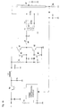
- Fig. 1 is an equivalent circuit diagram showing Embodiment 1 of the present invention.
- reference symbol T1 designates a step-up transformer which has a leakage flux property and which has a center tap.
- the step-up transformer T1 has a leakage inductance Ls.
- a secondary side winding of the step-up transformer T1 constitutes a distributed constant delay circuit which has a distributed capacitance Cw.
- reference symbol Ca designates a capacitor which is suitably added in order to adjust a resonance frequency
- reference symbol Cs designates a stray capacitance which is generated in the vicinity of a discharge lamp.
- Reference symbols Q1 and Q2 designate transistors constituting switching method, respectively.
- Collectors of the transistors Q1 and Q2 are connected to a leading end and a trailing end of a primary winding of the transformer T1.
- a transformer T2 is a current transformer, and opposite ends of its primary side winding are connected to emitters of the transistors Q1 and Q2 so as to detect emitter currents which are caused to flow through the transistors Q1 and Q2, respectively. Also, the connection is made so that the currents detected by the transformer T2 are positively fed back to bases of the transistors Q1 and Q2, respectively.
- the primary winding of the transformer T2 has a center tap
- the primary winding of the transformer T2 may be divided into two parts in order to detect the current caused to flow through the collector windings of the transistors.
- Capacitance components Cw, Ca and Cs of the secondary side circuit are composed with one another to form a resonance capacitor.
- the resonance capacitor constitutes together with a leakage inductance Ls a series resonance circuit as shown in Fig. 2.
- Fig. 2 is an equivalent circuit diagram showing a resonance circuit on a secondary side of the step-up transformer T1.
- reference symbol Z designates an impedance of the discharge lamp.
- reference symbols N1 and N2 designate the number of turns of the primary winding, and the number of turns of the secondary winding, respectively.
- An oscillation frequency of the inverter circuit is determined by a resonance frequency of the secondary side circuit.
- a slightly low frequency becomes the oscillation frequency of the current resonance type circuit based on an operation of a parallel loaded serial resonance circuit.
- the impedance of the discharge lamp has been about 100 k ⁇
- the operating frequency of the inverter circuit has been about 60 kHz.
- a proper value of the leakage inductance Ls has been in the range of 240 to 280 mH
- a proper value of the secondary side capacitance has been in the range of 25 to 30 pF.
- the leakage inductance Ls and the reactance of the secondary side capacitance at 60 kHz have been about 100 k ⁇ each, and a value which nearly agrees with the impedance of the discharge lamp has been a proper value therefor.
- a Q value of the resonance circuit in this case is about 1 or a value slightly larger than 1. In a case of the separately excited fixed frequency method, increasing excessively the Q value is not preferable from a viewpoint of the reliability of the circuit.
- the leakage inductance Ls is made small and the secondary side capacitance is made relatively large.
- this circuit is the parallel loaded serial resonance circuit in which in the secondary side resonance circuit, the load is connected in parallel with the capacitance component of the series resonance circuit, when the Q value becomes smaller than 1, the circuit does not continue to oscillate.
- the circuit is basically of the current resonance type. Thus, no oscillation is activated after the power source is turned ON unless any activating method is provided.
- Fig. 3 is an equivalent circuit diagram showing Embodiment 2 of the present invention.
- a DC-DC converter circuit is additionally provided in a preceding state of the circuit of Embodiment 1 shown in Fig. 1.
- a resistor R1, a capacitor C1, a thyristor S1, and a diode D1 constitute an activating circuit thereof.
- Rt and Ct are time constants on which a switching frequency of the DC-DC converter depends, these time constants are set irrespective of the oscillation frequency of the current resonance type circuit provided in a subsequent stage.
- Reference symbol Qs designates switching method of the DC-DC converter
- reference symbol Ds designates a fly-wheel diode which makes an important operation as well which will be described later.
- reference symbol Dr designates a regenerative diode.
- the transistors Q1 and Q2, the switching method Qs, the fly-wheel diode Ds, and the regenerative diode Dr may be replaced with switching method comprised of a MOS-FET or the like.
- the current resonance type self-oscillation circuit may be replaced with a half-bridge type current resonance circuit or the like as shown in Fig. 4. That is, Fig. 4 shows an equivalent circuit diagram when Embodiment 2 of the present invention is implemented for a conventional half-bridge type current resonance circuit.
- the one feature of the present invention is that no smoothing capacitor is provided right behind the fly-wheel diode Ds or the choke coil Le.
- the one feature of the present invention is not that the mere DC-DC converter is provided.
- another feature of the present invention is that the choke coil Lc of the DC-DC converter circuit is not made essential.
- the inductance corresponding to the choke coil Lc corresponds to a primary side leakage inductance of the step-up transformer T1.
- the step-up transformer T1 needs to be a leakage flux type transformer.
- an inductor may be suitably added. Consequently, the present invention does not exclude the choke coil which is suitably inserted.
- the principal object of the present invention is to make the switching timing of the switching method Qs constituting the switching method have no connection with the oscillation frequency of the inverter circuit. From this, in the current resonance type circuit, the phase of the effective value of the voltage applied to the primary winding of the transformer becomes nearly equal to that of the current caused to flow through the primary winding of the transformer, and thus the power factor is improved.
- Fig. 5 is an equivalent circuit diagram showing Embodiment 3 of the present invention.
- Emitters of transistors Q1 and Q2 constituting switching method are connected to the ground through current detecting resistors R4 and R5, respectively.
- the current detecting resistors R4 and R5 are resistors for detecting a resonance circuit.
- Amplifiers A1 and A2 serve to detect a voltage developed across the resistor R4, and a voltage developed across the resistor R5, respectively.
- Differentiating circuits F1 and F2 shape the detected voltages, respectively, and a composite signal is supplied to a triangular wave generating circuit F3 and a frequency dividing circuit Dv, respectively.
- the transistors Q1 and Q2 are driven by a voltage which is obtained through the frequency division in the frequency dividing circuit Dv.
- the structure of the current resonance type self-oscillation circuit is realized.
- the frequency dividing circuit Dv is made serve as a function as well of a multi vibrator, whereby the frequency dividing circuit Dv can also be made method for activating the current resonance type circuit.
- a lamp current of the discharge lamp is amplified by the error amplifier A3 and compared with the triangular wave signal in a comparator A4, thereby generating a switching signal of the switching method Q2.
- Figs. 6A to 6K show waveforms in the respective portions of the control circuit.
- the switching operations of the transistors Q1 and Q2 constituting the switching method are performed at timing at which a current It caused to flow through the primary winding of the step-up transformer T1 becomes zero. Hence, the phase of the current phase and the phases of the switching signals of the transistors Q1 and Q2 are equal to each other.
- the switching operation of the switching method Qs is performed at timing at which the waveform of the current caused to flow through the step-up transformer T1 becomes symmetrical about its peak. Consequently, the phase of the effective value of the voltage applied to the primary winding of the step-up transformer T1 becomes equal to that of the current, and thus the power factor is improved.
- Fig. 7 is a circuit diagram showing an example of the current resonance type circuit self-containing a synchronously oscillating circuit which serves as method as well for activating the current resonance type circuit and serves to shape the waveform of the detected current and uniform the output waveform at given intervals.
- This synchronous oscillation circuit may be any of a resonance leading-in type, a relaxation oscillation type, a PLL type, etc. Operation
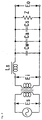
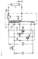
- Fig. 8 is an equivalent circuit diagram of the secondary side resonance circuit including up to the primary side driving circuit of the step-up transformer, and shows a relationship between the step-up transformer and the cold cathode fluorescent lamp in the inverter circuit for a cold cathode fluorescent lamp.
- the step-up transformer is expressed in the form of a three-terminal equivalent circuit.
- the three-terminal equivalent circuit is referred to as "a tank circuit" in U.S. Patent No. 6114814-B1, U.S. Patent Nos. 6,633,138 and 6,259,615, and Japanese Unexamined Patent Publication No. 2002-233158, while it is referred to as "a resonance circuit" in the resonance circuit described in Japanese Unexamined Patent Publication No.
- reference symbol C1 designates a coupling capacitor on the primary side which is inserted if necessary for the purpose of cutting a D.C. component in the current resonance type circuit, or for the purpose of cutting a D.C. component due to unbalance of the switching when the driving method is composed of a full-fridge (F-Bridge) circuit. It is generally advisable in the inverter circuit for a cold cathode fluorescent lamp that the coupling capacitor C1 having a sufficiently large capacitance value is inserted, thereby preventing the coupling capacitor C1 from participating in the resonance. This technical idea is different from that for the current resonance type inverter circuit for a hot cathode lamp. It should be noted that when the coupling capacitor C1 is made participate in the resonance, the exothermic quantity of inverter circuit increases and thus the conversion efficiency is reduced.
- Reference symbol Le designates a leakage inductance of the transformer (scientific society) which is distinguished from a leakage inductance Ls (JIS) measured by utilizing the JIS measuring method.
- Reference symbol M designates a mutual inductance.
- Reference symbol Cw designates a distributed capacitance of the secondary winding
- reference symbol Ca designates a resonance capacitance which is suitably added in order to adjust a resonance frequency
- reference symbol Cs designates a stray capacitance which is generated in the vicinity of the discharge lamp.
- the distributed capacitance Cw, the resonance capacitance Ca, and the stray capacitance Cs are composed with one another to form a resonance capacitance on the secondary side.
- reference symbol Z designates an impedance of the discharge lamp.
- a resonance current is disposed on a primary side of a transformer, and detects an input current on the primary side of the transformer.
- an axis of abscissa represents the driving frequency of the inverter circuit.
- Fig. 9A is a graphical representation showing phase characteristics of the voltage and the current when viewed from the primary side of the transformer.
- Fig. 9B is a graphical representation showing transfer characteristics of the voltage applied to the impedance Z of the discharge lamp.
- the impedance Z of the discharge lamp is changed in three stages: a first stage a represents a case of a large impedance; a second stage b represents a case of a middle impedance; and a third stage c represents a case of a small impedance.
- the resonance circuit In the half-bridge type current resonance circuit which is generally used as a lighting circuit for a hot cathode lamp, the resonance circuit is connected in series with a load and thus has no step-up operation for the load during a stationary discharge phase.
- the resonance circuit on the secondary side becomes the parallel loaded serial resonance circuit, it has the step-up operation for the load even during the stationary discharge phase.
- the driving frequency of the inverter circuit is determined at a frequency at which the phase characteristic curve crosses a line representing a phase lag of 0 degree.
- the phase of the current detected by the detecting method 1 shown in Fig. 8 lags the phase of the resonance current.
- the inverter circuit oscillates at a lower frequency than the resonance frequency of the resonance circuit.
- no frequency is obtained at which the phase characteristic curve crosses the line representing the phase lag of 0 degree.
- the condition of the large Q value advantageously functions in the present invention.
- the reason for this is that the resonance current of the secondary side circuit becomes much and the oscillation of the current resonance type circuit is stabilized as the Q value becomes larger.
- this method that the step-up ratio of the step-up transformer also increases.
- the resonance circuit having the large Q value it is required that the number of turns of the secondary wiring of the step-up transformer is made smaller than that of the secondary winding in the case of the conventional separately excited driving method and also the value of the capacitance component on the secondary side is set as large. Since the value of the leakage inductance is proportional to a square of the number of turns of the secondary winding, it is largely reduced by only slightly reducing the number of turns. As a result, since a ratio of transformation required to obtain the necessary voltage can be made small, the step-up transformer can be further miniaturized.
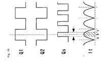
- Figs. 10A to 10D are waveform diagrams explaining a relationship between the switching timing of the respective switching method and the current in Embodiment 3.
- the switching method Qs is synchronized in switching timing with the transistors Q1 and Q2, and the switching of the switching method Qs is performed so that the phases of the currents caused to flow through the transistors Q1 and Q2, and the phase of the effective value of the voltage applied to the primary winding of the step-up transformer T1 become equal to each other.
- a current which is caused to flow through the center tap of the step-up transformer T1 is expressed in the form of It shown in Fig. 10D.
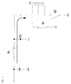
- Fig. 12 shows schematically a flow of the current to the utmost. Actually, a large oscillating current is often caused to flow through the primary winding of the step-up transformer.
- Figs. 13A and 13B are waveform diagrams showing a situation of oscillation of the current at timing indicated by c shown in Fig. 10D.
- the same state as that in which the primary winding of the step-up transformer T1 is short-circuited is provided for the resonance current which is caused to flow in the forward direction, thereby preventing the energy of the resonance current from being lost.
- the oscillating current which is caused to flow in the reverse direction is regenerated in the power source, thereby damping the oscillation energy.
- the dimming circuit using the conventional DC-DC converter includes no method for selectively damping only such a regenerative current. Thus, since the energy of the oscillating current is accumulated, the undesired current oscillation is caused in the primary winding.
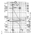
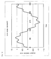
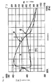
- Fig. 15 is a graphical representation explaining that many self-resonances exist on the secondary winding of the step-up transformer for a high voltage.
- a characteristic curve Z of Fig. 15 is obtained by measuring the impedance characteristics from the primary winding side. As apparent from the characteristic curve Z of Fig. 15, a plurality of resonances appear.
- a resonance indicated by A is one called the generally well known self-resonance of the transformer.
- self-resonances indicated by B, C and D also exist.
- the self-resonance indicated by B has a large energy and thus may appear in the form of a current oscillation on the primary winding side.
- Such current oscillations are described as "the undesired resonances" in Japanese Unexamined Patent Publication No. Sho 56-88678 as well, etc.
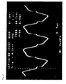
- Fig. 16 is a graphical representation showing a situation of an oscillating current which is actually generated in the primary winding of the step-up transformer for a cold cathode fluorescent lamp. It is understood from Fig. 16 that the current which is caused to flow through the primary winding is not an ideal sine wave, and the undesired high-order resonance currents are superposed on the current in the primary winding. When a frequency which is an integral multiple of the driving frequency of the inverter circuit agrees with the high-order resonance frequency shown in Fig. 16, the resonance phenomenon of the undesired current becomes remarkable.
- Such an undesired resonance exerts a bad influence on the switching timing of the transistors Q1 and Q2.
- the circuit using the zero current switching method for detecting the zero current to determine the switching timing as disclosed in Japanese Unexamined Patent Publication No. Sho 59-032370, U.S. Patent No. 6,633,138, Japanese Unexamined Patent Publication No. Hei 8-288080, etc. is seriously influenced by such an undesired resonance. Consequently, it is effective to damp the oscillating current by using the regenerating method as described above.
Landscapes
- Engineering & Computer Science (AREA)
- Power Engineering (AREA)
- Inverter Devices (AREA)
- Circuit Arrangements For Discharge Lamps (AREA)
Applications Claiming Priority (1)
| Application Number | Priority Date | Filing Date | Title |
|---|---|---|---|
| JP2004318059A JP5048920B2 (ja) | 2004-11-01 | 2004-11-01 | 電流共振型インバータ回路と電力制御手段 |
Publications (2)
| Publication Number | Publication Date |
|---|---|
| EP1653786A2 true EP1653786A2 (de) | 2006-05-03 |
| EP1653786A3 EP1653786A3 (de) | 2008-07-09 |
Family
ID=35708962
Family Applications (1)
| Application Number | Title | Priority Date | Filing Date |
|---|---|---|---|
| EP05256722A Withdrawn EP1653786A3 (de) | 2004-11-01 | 2005-10-31 | Stromresonanzumrichter und Verfahren zur Leistungssteuerung |
Country Status (6)
| Country | Link |
|---|---|
| US (1) | US7453216B2 (de) |
| EP (1) | EP1653786A3 (de) |
| JP (1) | JP5048920B2 (de) |
| KR (1) | KR20060052267A (de) |
| CN (1) | CN1802059A (de) |
| TW (1) | TW200616495A (de) |
Families Citing this family (23)
| Publication number | Priority date | Publication date | Assignee | Title |
|---|---|---|---|---|
| JP2005312284A (ja) * | 2005-01-12 | 2005-11-04 | Masakazu Ushijima | 電流共振型放電管用インバータ回路 |
| JP4908760B2 (ja) | 2005-01-12 | 2012-04-04 | 昌和 牛嶋 | 電流共振型インバータ回路 |
| CN1832321B (zh) * | 2005-03-07 | 2011-09-14 | 柏怡国际股份有限公司 | 换流装置 |
| JP2008159545A (ja) * | 2006-12-26 | 2008-07-10 | Sanken Electric Co Ltd | 冷陰極管蛍光灯インバータ装置 |
| JP2008251339A (ja) * | 2007-03-30 | 2008-10-16 | Sony Corp | 蛍光管駆動方法および装置 |
| JP2008287979A (ja) * | 2007-05-16 | 2008-11-27 | Minebea Co Ltd | 放電灯点灯装置 |
| CN101272098B (zh) * | 2008-04-08 | 2010-11-03 | 广州金升阳科技有限公司 | 双三极管电流控制型自振荡反激变换器 |
| JP5149686B2 (ja) * | 2008-04-24 | 2013-02-20 | パナソニック株式会社 | 電力変換装置及びそれを用いた放電灯点灯装置、並びに車両用前照灯装置 |
| CN101568216B (zh) * | 2008-04-25 | 2012-09-26 | 群康科技(深圳)有限公司 | 逆变电路和液晶显示装置 |
| WO2009139077A1 (ja) * | 2008-05-15 | 2009-11-19 | 国立大学法人 東京工業大学 | 交流電圧制御装置 |
| US9413314B2 (en) | 2009-05-08 | 2016-08-09 | Federal-Mogul Ignition Company | Corona ignition with self-tuning power amplifier |
| CN102459863A (zh) * | 2009-05-08 | 2012-05-16 | 费德罗-莫格尔点火公司 | 具有自调节功率放大器的电晕点火系统 |
| US8289734B2 (en) * | 2009-10-15 | 2012-10-16 | Ansaldo Sts Usa, Inc. | Output apparatus to output a vital output from two sources |
| CN102291001B (zh) * | 2011-08-26 | 2014-01-01 | 广州金升阳科技有限公司 | 一种自激推挽式变换器 |
| US20130200798A1 (en) * | 2012-02-07 | 2013-08-08 | Laurence P. Sadwick | Fluorescent Lamp Dimmer |
| JP6005502B2 (ja) * | 2012-12-18 | 2016-10-12 | 新電元工業株式会社 | 電源装置 |
| TWI641290B (zh) * | 2013-02-06 | 2018-11-11 | 英諾系統公司 | 螢光燈調光器 |
| WO2015105171A1 (ja) * | 2014-01-10 | 2015-07-16 | 株式会社村田製作所 | 高圧電源装置 |
| TWI556203B (zh) * | 2015-01-30 | 2016-11-01 | 友達光電股份有限公司 | 顯示器與控制轉換器的方法 |
| CN106329977B (zh) * | 2015-07-03 | 2018-10-09 | 台达电子工业股份有限公司 | 逆变电路的控制方法 |
| TWI777412B (zh) * | 2020-06-29 | 2022-09-11 | 立錡科技股份有限公司 | 諧振半橋返馳電源供應器及其一次側控制電路與控制方法 |
| CN119726993B (zh) * | 2023-09-27 | 2026-03-27 | 安克创新科技股份有限公司 | 一种电路控制方法、装置、存储介质及电子设备 |
| US12706460B2 (en) * | 2025-01-16 | 2026-08-11 | Shenzhen Gospell Digital Technology Co., Ltd | Single-stage bidirectional DC converter and single-phase user-side energy storage inverter based on single-stage bidirectional DC converter |
Citations (9)
| Publication number | Priority date | Publication date | Assignee | Title |
|---|---|---|---|---|
| JPS5688678A (en) | 1979-12-19 | 1981-07-18 | Toshiba Electric Equip Corp | Transistor inverter |
| JPS5932370A (ja) | 1982-08-16 | 1984-02-21 | Hitachi Ltd | 高圧電源装置 |
| JPH07211472A (ja) | 1994-01-24 | 1995-08-11 | Hitachi Media Electron:Kk | 点灯装置 |
| US5495405A (en) | 1993-08-30 | 1996-02-27 | Masakazu Ushijima | Inverter circuit for use with discharge tube |
| JPH08288080A (ja) | 1995-04-17 | 1996-11-01 | Nakano Denki Seisakusho:Kk | 放電灯点灯装置 |
| US6114814A (en) | 1998-12-11 | 2000-09-05 | Monolithic Power Systems, Inc. | Apparatus for controlling a discharge lamp in a backlighted display |
| US6259615B1 (en) | 1999-07-22 | 2001-07-10 | O2 Micro International Limited | High-efficiency adaptive DC/AC converter |
| JP2002233158A (ja) | 1999-11-09 | 2002-08-16 | O2 Micro Internatl Ltd | 高効率適応型dc/acコンバータ |
| JP2003168585A (ja) | 2001-09-21 | 2003-06-13 | Minebea Co Ltd | 放電管用インバータ回路 |
Family Cites Families (13)
| Publication number | Priority date | Publication date | Assignee | Title |
|---|---|---|---|---|
| JPS6024190U (ja) * | 1983-07-20 | 1985-02-19 | 富士電気化学株式会社 | プツシユプルコンバ−タの偏磁防止回路 |
| JPH06125513A (ja) * | 1992-10-13 | 1994-05-06 | Sharp Corp | テレビジョン受像機の電源回路 |
| US5382882A (en) | 1993-04-20 | 1995-01-17 | General Electric Company | Power supply circuit for a gas discharge lamp |
| JP3443654B2 (ja) * | 1994-11-24 | 2003-09-08 | ミネベア株式会社 | 電圧共振型インバータ回路 |
| JP3292788B2 (ja) * | 1995-03-29 | 2002-06-17 | 昌和 牛嶋 | 放電管用インバータ回路 |
| JP3547837B2 (ja) * | 1995-03-31 | 2004-07-28 | ミネベア株式会社 | インバ−タ装置 |
| JP3273161B2 (ja) * | 1996-06-11 | 2002-04-08 | シャープ株式会社 | 負荷駆動回路 |
| US6081439A (en) * | 1996-06-19 | 2000-06-27 | Kijima Co., Ltd. | Inverter provided with output regulating mechanism |
| US5619106A (en) * | 1996-06-24 | 1997-04-08 | General Electric Company | Diodeless start circiut for gas discharge lamp having a voltage divider connected across the switching element of the inverter |
| JPH11215826A (ja) * | 1998-01-21 | 1999-08-06 | Hitachi Ltd | 自励発振型電流共振コンバータ |
| JP3705966B2 (ja) * | 1999-09-07 | 2005-10-12 | 東光株式会社 | スイッチング電源回路 |
| TW515224B (en) * | 2001-03-07 | 2002-12-21 | Ambit Microsystems Corp | Inverter and lamp ignition system using the same |
| US6570344B2 (en) * | 2001-05-07 | 2003-05-27 | O2Micro International Limited | Lamp grounding and leakage current detection system |
-
2004
- 2004-11-01 JP JP2004318059A patent/JP5048920B2/ja not_active Expired - Fee Related
-
2005
- 2005-10-27 KR KR1020050101852A patent/KR20060052267A/ko not_active Ceased
- 2005-10-31 TW TW094138093A patent/TW200616495A/zh not_active IP Right Cessation
- 2005-10-31 EP EP05256722A patent/EP1653786A3/de not_active Withdrawn
- 2005-10-31 US US11/261,492 patent/US7453216B2/en not_active Expired - Fee Related
- 2005-10-31 CN CNA2005101188108A patent/CN1802059A/zh active Pending
Patent Citations (11)
| Publication number | Priority date | Publication date | Assignee | Title |
|---|---|---|---|---|
| JPS5688678A (en) | 1979-12-19 | 1981-07-18 | Toshiba Electric Equip Corp | Transistor inverter |
| JPS5932370A (ja) | 1982-08-16 | 1984-02-21 | Hitachi Ltd | 高圧電源装置 |
| US5495405A (en) | 1993-08-30 | 1996-02-27 | Masakazu Ushijima | Inverter circuit for use with discharge tube |
| JP2733817B2 (ja) | 1993-08-30 | 1998-03-30 | 昌和 牛嶋 | 放電管用インバーター回路 |
| JPH07211472A (ja) | 1994-01-24 | 1995-08-11 | Hitachi Media Electron:Kk | 点灯装置 |
| JPH08288080A (ja) | 1995-04-17 | 1996-11-01 | Nakano Denki Seisakusho:Kk | 放電灯点灯装置 |
| US6114814A (en) | 1998-12-11 | 2000-09-05 | Monolithic Power Systems, Inc. | Apparatus for controlling a discharge lamp in a backlighted display |
| US6633138B2 (en) | 1998-12-11 | 2003-10-14 | Monolithic Power Systems, Inc. | Method and apparatus for controlling a discharge lamp in a backlighted display |
| US6259615B1 (en) | 1999-07-22 | 2001-07-10 | O2 Micro International Limited | High-efficiency adaptive DC/AC converter |
| JP2002233158A (ja) | 1999-11-09 | 2002-08-16 | O2 Micro Internatl Ltd | 高効率適応型dc/acコンバータ |
| JP2003168585A (ja) | 2001-09-21 | 2003-06-13 | Minebea Co Ltd | 放電管用インバータ回路 |
Also Published As
| Publication number | Publication date |
|---|---|
| JP2006129669A (ja) | 2006-05-18 |
| JP5048920B2 (ja) | 2012-10-17 |
| KR20060052267A (ko) | 2006-05-19 |
| CN1802059A (zh) | 2006-07-12 |
| US7453216B2 (en) | 2008-11-18 |
| TW200616495A (en) | 2006-05-16 |
| US20060164024A1 (en) | 2006-07-27 |
| TWI312261B (de) | 2009-07-11 |
| EP1653786A3 (de) | 2008-07-09 |
Similar Documents
| Publication | Publication Date | Title |
|---|---|---|
| US7453216B2 (en) | Current resonance type inverter circuit and power controlling method | |
| KR100845663B1 (ko) | 방전 램프의 구동을 위한 dc/ac 전력 변환을 위한 방법및 장치 | |
| JP4908760B2 (ja) | 電流共振型インバータ回路 | |
| JP3443654B2 (ja) | 電圧共振型インバータ回路 | |
| KR101217372B1 (ko) | 전류 공진형 방전관용 인버터 회로 | |
| JPH06176881A (ja) | 安定器回路 | |
| CN101523711A (zh) | 自振荡直流-直流转换器及其方法 | |
| CN101013852A (zh) | 开关电源电路 | |
| WO2013026267A1 (zh) | 一种自激推挽式变换器 | |
| JP2003516705A (ja) | 電流及び電圧フィードバック経路を有する電子安定器 | |
| JPH03212171A (ja) | 高周波加熱装置用スイッチング電源 | |
| US6788005B2 (en) | Inverter and lamp ignition system using the same | |
| JP2003235259A (ja) | スイッチング電源回路 | |
| US20040004439A1 (en) | High frequency heating device | |
| CN202206638U (zh) | 荧光灯异常状态保护检测电路 | |
| HK1088169A (en) | Current resonance type inverter circuit and power controlling method | |
| JP4993548B2 (ja) | 自励式インバータ駆動回路 | |
| JP2004524669A (ja) | E級駆動回路により駆動される共振ハーフブリッジ変換器を有する放電ランプ用回路配置 | |
| CN115622408B (zh) | 一种原边反馈变换器、及其动态响应优化方法和装置 | |
| JP2006222076A (ja) | 電流共振型放電管用インバータ回路 | |
| JPH09260076A (ja) | 冷陰極蛍光灯の点灯調光回路 | |
| Lin et al. | Three-phase electronic ballast with current-equalization function | |
| Chang et al. | Development of lighting source with CCFL in T8-tube | |
| JPH11102796A (ja) | 放電灯点灯装置 | |
| CN101300906B (zh) | 用于电子镇流器的可切换的加热变压器的驱动电路以及相应的方法 |
Legal Events
| Date | Code | Title | Description |
|---|---|---|---|
| PUAI | Public reference made under article 153(3) epc to a published international application that has entered the european phase |
Free format text: ORIGINAL CODE: 0009012 |
|
| AK | Designated contracting states |
Kind code of ref document: A2 Designated state(s): AT BE BG CH CY CZ DE DK EE ES FI FR GB GR HU IE IS IT LI LT LU LV MC NL PL PT RO SE SI SK TR |
|
| AX | Request for extension of the european patent |
Extension state: AL BA HR MK YU |
|
| REG | Reference to a national code |
Ref country code: HK Ref legal event code: DE Ref document number: 1088169 Country of ref document: HK |
|
| PUAL | Search report despatched |
Free format text: ORIGINAL CODE: 0009013 |
|
| AK | Designated contracting states |
Kind code of ref document: A3 Designated state(s): AT BE BG CH CY CZ DE DK EE ES FI FR GB GR HU IE IS IT LI LT LU LV MC NL PL PT RO SE SI SK TR |
|
| AX | Request for extension of the european patent |
Extension state: AL BA HR MK YU |
|
| AKX | Designation fees paid | ||
| REG | Reference to a national code |
Ref country code: DE Ref legal event code: 8566 |
|
| STAA | Information on the status of an ep patent application or granted ep patent |
Free format text: STATUS: THE APPLICATION IS DEEMED TO BE WITHDRAWN |
|
| 18D | Application deemed to be withdrawn |
Effective date: 20090110 |
|
| REG | Reference to a national code |
Ref country code: HK Ref legal event code: WD Ref document number: 1088169 Country of ref document: HK |