EP1674902A1 - Mehrkanalige optische wegwechseleinrichtung und herstellungsverfahren dafür - Google Patents
Mehrkanalige optische wegwechseleinrichtung und herstellungsverfahren dafür Download PDFInfo
- Publication number
- EP1674902A1 EP1674902A1 EP04792303A EP04792303A EP1674902A1 EP 1674902 A1 EP1674902 A1 EP 1674902A1 EP 04792303 A EP04792303 A EP 04792303A EP 04792303 A EP04792303 A EP 04792303A EP 1674902 A1 EP1674902 A1 EP 1674902A1
- Authority
- EP
- European Patent Office
- Prior art keywords
- core
- resin
- optical path
- forming
- multichannel
- Prior art date
- Legal status (The legal status is an assumption and is not a legal conclusion. Google has not performed a legal analysis and makes no representation as to the accuracy of the status listed.)
- Withdrawn
Links
Images





Classifications
-
- G—PHYSICS
- G02—OPTICS
- G02B—OPTICAL ELEMENTS, SYSTEMS OR APPARATUS
- G02B6/00—Light guides; Structural details of arrangements comprising light guides and other optical elements, e.g. couplings
- G02B6/10—Light guides; Structural details of arrangements comprising light guides and other optical elements, e.g. couplings of the optical waveguide type
- G02B6/12—Light guides; Structural details of arrangements comprising light guides and other optical elements, e.g. couplings of the optical waveguide type of the integrated circuit kind
-
- G—PHYSICS
- G02—OPTICS
- G02B—OPTICAL ELEMENTS, SYSTEMS OR APPARATUS
- G02B6/00—Light guides; Structural details of arrangements comprising light guides and other optical elements, e.g. couplings
- G02B6/10—Light guides; Structural details of arrangements comprising light guides and other optical elements, e.g. couplings of the optical waveguide type
- G02B6/12—Light guides; Structural details of arrangements comprising light guides and other optical elements, e.g. couplings of the optical waveguide type of the integrated circuit kind
- G02B6/122—Basic optical elements, e.g. light-guiding paths
-
- G—PHYSICS
- G02—OPTICS
- G02B—OPTICAL ELEMENTS, SYSTEMS OR APPARATUS
- G02B6/00—Light guides; Structural details of arrangements comprising light guides and other optical elements, e.g. couplings
- G02B6/10—Light guides; Structural details of arrangements comprising light guides and other optical elements, e.g. couplings of the optical waveguide type
- G02B6/12—Light guides; Structural details of arrangements comprising light guides and other optical elements, e.g. couplings of the optical waveguide type of the integrated circuit kind
- G02B6/12002—Three-dimensional structures
-
- G—PHYSICS
- G02—OPTICS
- G02B—OPTICAL ELEMENTS, SYSTEMS OR APPARATUS
- G02B6/00—Light guides; Structural details of arrangements comprising light guides and other optical elements, e.g. couplings
- G02B6/10—Light guides; Structural details of arrangements comprising light guides and other optical elements, e.g. couplings of the optical waveguide type
- G02B6/12—Light guides; Structural details of arrangements comprising light guides and other optical elements, e.g. couplings of the optical waveguide type of the integrated circuit kind
- G02B6/122—Basic optical elements, e.g. light-guiding paths
- G02B6/125—Bends, branchings or intersections
-
- G—PHYSICS
- G02—OPTICS
- G02B—OPTICAL ELEMENTS, SYSTEMS OR APPARATUS
- G02B6/00—Light guides; Structural details of arrangements comprising light guides and other optical elements, e.g. couplings
- G02B6/10—Light guides; Structural details of arrangements comprising light guides and other optical elements, e.g. couplings of the optical waveguide type
- G02B6/12—Light guides; Structural details of arrangements comprising light guides and other optical elements, e.g. couplings of the optical waveguide type of the integrated circuit kind
- G02B2006/12166—Manufacturing methods
- G02B2006/12176—Etching
Definitions
- the present invention relates to a multichannel optical path changing device that has little loss and even characteristics and to its effective production method.
- optical waveguide becomes more and more important as an optical network key device, and its development is proceeding toward the application to optical electronic circuit wiring substrate and the like.
- Resin-made optical waveguides which are easy in handling, have been developed as their powerful candidates.
- waveguide-use resin materials there are used fluorinated polyimide resin, deuterated polysiloxane resin, epoxy resin, perfluorinated alicyclic resin, acrylic resin, silicone resin and the like.
- optical path changing technique that sharply bends an optical circuit in order have an efficient connection between devices, particularly a multichannel optical path changing device that can send and receive a plurality of optical signals in parallel, such as 2-16 channels. Furthermore, there is a demand for an optical path changing device that has little loss, even characteristics between channels, and low cost.
- a multichannel optical path changing member produced by opposing inclined end surfaces of a pair of optical waveguides that have the inclined end surfaces at one ends and roughly identical inclination angles of the inclined end surfaces and the optical waveguide core sizes, arrangements and the like in the inclined end surfaces, by connecting the inclined end surfaces with each other in a manner that the cores of the waveguides in the inclined end surfaces roughly coincide with each other, by fixing the pair of optical waveguides to have a rough V-shape, by removing an apex portion of the V-shaped optical waveguide to expose the core to a predetermined position, by laminating in parallel ones provided with reflecting surfaces at predetermined intervals, and by covering that with a substance having a refractive index lower than that of the core (see Patent Publication 1).
- a resin-made multichannel optical path changing device that has monolithically formed cores having a mirror therebetween and optical path directions changed, and that has multichannel cores simultaneously formed under a condition that their positional relationship is maintained.
- the above multichannel optical path changing device can be produced by a first or second method of the present invention.
- the first method of the present invention includes steps of forming a parallelepiped block on a substrate by a cladding resin; forming a film of a core layer to cover the block by a core resin; and simultaneously forming cores having an optical path direction rectangularly changed, by selectively etching the core layer and the block.
- the second method of the present invention includes steps of forming a film of a core layer on a substrate by a resin; and simultaneously forming cores having an optical path rectangularly changed, by selectively etching the core layer, under a condition that their positional relationship is maintained.
- Fig. 1 is a view showing an example of steps of producing a multichannel optical path changing device according to the first method of the present invention
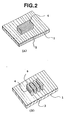
- Fig. 2(A) shows a cladding block
- Fig. 2(B) shows a core in which a horizontal portion and a vertical portion are monolithically formed
- Fig. 3 is a view showing a relationship between a core block and a core in Example 1
- Fig. 4 is a view showing a first example of steps of producing a multichannel optical path changing device according to the second method of the present invention;
- Fig. 4 is a view showing a first example of steps of producing a multichannel optical path changing device according to the second method of the present invention
- Fig. 4 is a view showing a first example of steps of producing a multichannel optical path changing device according to the second method of the present invention
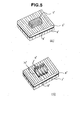
- FIG. 5(A) shows a core block
- Fig. 5(B) shows a core in which a horizontal portion and a vertical portion are monolithically formed
- Fig. 6 is a view showing a relationship between a core block and a core in Example 2
- Fig. 7 is a view showing a second example of steps of producing a multichannel optical path changing device according to the second method of the present invention
- Fig. 8 shows a perspective view of a core in the step (e) of Fig. 7.
- vertical and horizontal portions of a waveguide core are monolithically formed in a wafer process. Therefore, it is possible to provide a multichannel optical path changing device with stable characteristics, high precision, low loss and low cost.
- FIG. 1(a) to Fig. 1(j) are views illustrating one example of steps of producing a multichannel optical path changing device of the present invention.
- a multichannel optical path changing device is produced by the following steps.
- a film of a sacrifice layer 2, which is a metal film that dissolves in acid is formed on a temporary substrate by using a technique such as magnetron sputtering.
- the sacrifice layer 2 may be made of a water-soluble resin.
- a film of a cladding layer 3 is formed.
- a cladding block 4 is produced by a technique of photolithography and Reactive Ion Etching (RIE). This block 4 is parallelepiped. Regarding its size, a size that is necessary for an optical path changing device to be produced is suitably selected. This block may be produced for each device. However, it is also preferable to produce continuous ones at one time in line for parallel devices.
- a perspective view of the cladding block 4 is shown in Fig. 2(A). In this step, the production is possible by a direct exposure method, mold method, or a method using a dicing saw.
- the entire surface is filled with a cladding layer 7.
- a V-groove is formed by a dicing saw, and a reflecting mirror 9 is formed by using a technique such as magnetron sputtering to form a mirror.
- the reflecting mirror there is used a metal film, a dielectric multilayer film or the like.
- a method in which a prism having a reflecting film formed thereon is disposed in the V-groove and then it is fixed by adhesive or the like.
- the V-groove is filled with a cladding resin 10 to make the device surface flat.
- a substrate 11 is attached to the wavelength.
- the substrate it is possible to use a glass substrate, silicon substrate, resin substrate or the like.
- the sacrifice layer 2 is removed by acid or the like, then the temporary substrate 1 is removed, and then it is cut and separated into a multichannel optical path changing device by a dicing saw.
- FIG. 4(a) to Fig. 4(1) are views illustrating the first example of the steps (the second method) of producing a multichannel optical path changing device of the present invention.
- a multichannel optical path changing device is produced by the following steps.
- a film of a sacrifice layer 2' which is a metal film of Al, Cu or the like that dissolves in acid, is formed on a first temporary substrate 1' by using a technique such as magnetron sputtering.
- the sacrifice layer 2 may be made of a water-soluble resin.
- a film of a cladding layer 3' is formed.
- Fig. 4(b) a film of a cladding layer 3' is formed.
- a film of a core layer 4' is formed.
- a core block 5' is produced by a technique of photolithography and Reactive Ion Etching (RIE).
- RIE Reactive Ion Etching
- This block 5' is parallelepiped.
- a size that is necessary for an optical path changing device to be produced is suitably selected.
- This block may be produced for each device. However, it is also preferable to produce continuous ones at one time in line for parallel devices.
- a perspective view of the core block 5' is shown in Fig. 5(A). In this step, the production is possible by a direct exposure method, mold method, or a method using a dicing saw.
- a film of a cladding layer 6' is formed to cover the core block 5'.
- an L-shaped core block is formed by removing a core resin of a part interposed between the core of a horizontal portion and the core of a vertical portion, which constitute an L-shape, by techniques of photolithography and Reactive Ion Etching.
- the entire surface is filled with a cladding layer 8', then the core resin and the cladding resin of unnecessary portions between channels and between devices are removed to form L-shaped cores 7' (7b'), then void spaces between channels and between devices are covered with cladding layers, and then the surface is subjected to a flattening treatment.
- FIG. 2(B) shows a perspective view of the multichannel cores 7' during this step.
- a second substrate 9' is attached by an adhesive 10', and the first temporary substrate 1' is removed.
- a V-groove is formed by a dicing saw, and a reflecting mirror 12' is formed at a corner portion by using a technique such as magnetron sputtering to form a mirror.
- the reflecting mirror there is used a metal film, a dielectric multilayer film or the like.
- a method in which a prism having a reflecting film formed thereon is disposed in the V-groove and then it is fixed by adhesive or the like.
- Fig. 4(j) the V-groove is filled with a cladding resin 13' to make the device surface flat.
- a substrate 14' is attached to the waveguide.
- the substrate it is possible to use a glass substrate, silicon substrate, resin substrate or the like.
- the sacrifice layer 2' is removed by acid or the like, then the second temporary substrate 9' is removed, and then it is cut and separated into a multichannel optical path changing device by a dicing saw, thereby producing a multichannel optical path changing.
- Fig. 7 is a view showing a second example of the method (second method) for producing a multichannel optical path chancing device according to the present invention.
- Fig. 7(a) shows one prepared by forming a film of a sacrifice layer 2' on a first temporary substrate 1' and then forming thereon a cladding layer 3' and a core layer 4'.
- a core resin of a part interposed between the core of a horizontal portion and the core of a vertical portion, which constitute an L-shape is removed by conducing a selective etching by techniques of photolithography and Reactive Ion Etching, thereby forming an L-shaped core block.
- the removed portion is filled with a cladding resin.
- Fig. 7(d) between waveguides and other core resin unnecessary portions are selectively removed to form L-shaped cores. Then, in Fig. 7(e), the removed portion is filled with a cladding resin, thereby simultaneously forming L-shaped cores under a condition that their respective positional relationships are maintained.
- Fig. 8 shows a perspective view upon this. After that, a multichannel optical path changing is produced by a method similar to that of Fig. 4(h) to Fig. 4(l) in the first example.
- the present invention relates to an optical path changing device that changes the direction of an optical path in a rectangular direction, it is easily possible to change an optical path at an angle other than right angle by adjusting inclination of the mirror portion.
- Example 1 corresponds to the first method of the present invention
- Examples 2-3 correspond to the second method of the present invention.
- the size of a core section (E-E view in Fig. 3) is a square of 40 ⁇ m ⁇ 40 ⁇ m, and the core pitch between channels is set to 0.25mm.
- a film of a sacrifice layer was formed on a 4-inch temporary glass substrate by using a magnetron sputtering. Al (thickness: about 1 ⁇ m) was used as the sacrifice layer. Then, a film of a cladding layer was formed. As the cladding, epoxy resin was used, and the film was formed by spin coating. After the film formation, a flattening treatment was conducted by grinding and polishing to adjust the thickness of the cladding layer to 70 ⁇ m. Then, a film of a masking member was formed on the cladding layer, and a patterning was conducted by photolithography. Al was used for the masking member.
- a parallelepiped block of the cladding was produced by removing (O 2 -RIE) an unnecessary portion of the cladding layer that is not protected with the mask layer through etching by allowing O 2 gas to flow thereinto.
- the cladding block was adjusted to 70 ⁇ m in height (A in Fig. 3) and to 1mm in width (B in Fig. 3). In a direction perpendicular to the paper surface of Fig. 3, cladding blocks of devices aligned are monolithically formed in line.
- a film of a core layer was formed thereon by spin coating.
- epoxy resin was used as the core layer.
- the top surface of the core layer was ground and polished to conduct a flattening treatment of the surface.
- the core layer thickness was adjusted to 40 ⁇ m from the cladding block top.
- a film of an Al masking member was formed on the core layer, and patterning was conducted by photolithography.
- unnecessary portions of the core layer and the cladding block were removed by O 2 -RIE, thereby producing a core that is rectangularly bent along the cladding block (Fig. 3).
- the core size is 40 ⁇ m ⁇ 40 ⁇ m (E-E view in Fig. 3), and the horizontal portion and the vertical portion are the same in size.
- the length of the core vertical portion is 110 ⁇ m from the top end of the core horizontal portion (C in Fig. 3).
- the length of the core horizontal portion is 1,040 ⁇ m from the outer end of the core vertical portion (D in Fig. 3).
- the entire surface was filled with a cladding resin.
- the top surface of the cladding resin was ground and polished to conduct a flattening treatment. Spin coating was used for filling of the cladding resin.
- a V-groove was formed at a right-angle bent portion of the core by a dicing saw to form a mirror surface.
- the mirror was formed in a manner to form an Au film only at the V-groove portion by magnetron sputtering.
- the V-groove was filled with a cladding resin, and a film of a cladding layer was formed. The surface was ground and polished to conduct a flattening treatment.
- a glass substrate was attached to the cladding layer's top surface by using an epoxy adhesive.
- the sacrifice layer was dissolved, and the temporary substrate was removed. To remove the sacrifice layer, a mixed liquid of copper sulfate, ferric chloride and water was used.
- each device was cut and separated into squares of 2mmx2mm, thereby obtaining 803 pieces of four-channel optical path changing devices. Insertion loss was measured by transmitting a light of 1.3 ⁇ m in wavelength. With this, 667 pieces (83%) were found to have a waveguide insertion loss in the device of 3dB or less and an insertion loss dispersion in the device of 0.1dB or less. Thus, it was possible to produce homogeneous, four-channel, optical path changing devices at one time with high yield.
- EXAMPLE 2 Four-channel optical path changing devices were produced.
- the size of a core section (K-K view in Fig. 6) is a square of 40 ⁇ m ⁇ 40 ⁇ m, and the core pitch between channels is set to 0.25mm.
- a film of a sacrifice layer was formed on a 4-inch temporary glass substrate by using a magnetron sputtering. Al (thickness: about 1 ⁇ m) was used as the sacrifice layer. Then, a film of a cladding layer of 10 ⁇ m was formed, and then a film of a core layer was formed. As the core, epoxy resin was used, and the film was formed by spin coating. After the film formation, a flattening treatment was conducted by grinding and polishing to adjust the thickness of the core layer to 120 ⁇ m. Then, a film of a masking member was formed on the core layer, and a patterning was conducted by photolithography. Al was used for the masking member. A parallelepiped block of the core was produced by removing (O 2 -RIE) an unnecessary portion of the core layer that is not protected with the mask layer through etching by allowing O 2 gas to flow thereinto.
- the core block was adjusted to 120 ⁇ m in height (G in Fig. 6) and to 1mm in width (F in Fig. 6). In a direction perpendicular to the paper surface of Fig. 6, core blocks of devices aligned are monolithically formed in line.
- a film of a cladding layer was formed thereon by spin coating.
- As the cladding layer an epoxy resin was used. After the film formation, the top surface of the cladding layer was ground and polished to conduct a flattening treatment of the surface. With this, the cladding layer thickness was adjusted to 10 ⁇ m from the core block top. Then, a film of an Al masking member was formed on the cladding layer, and patterning was conducted by photolithography. Then, unnecessary portions of the cladding layer and the core block were removed by O 2 -RIE, thereby producing a core that is rectangularly bent (Fig. 6).
- the core size is 40 ⁇ m ⁇ 40 ⁇ m (K-K view in Fig. 6), and the horizontal portion and the vertical portion are the same in size.
- the length of the core vertical portion is 120 ⁇ m from the bottom end of the core horizontal portion (G in Fig. 6).
- the length of the core horizontal portion is 1,000 ⁇ m from the outer end of the core vertical portion (F in Fig. 6).
- the entire surface was filled with a cladding resin.
- the top surface of the cladding resin was ground and polished to conduct a flattening treatment. Spin coating was used for filling of the cladding resin.
- a second temporary glass substrate was attached by an epoxy adhesive, the sacrifice layer was dissolved, and the first temporary substrate was removed. To remove the sacrifice layer, a mixed liquid of copper sulfate, ferric chloride and water was used.
- a V-groove was formed at a right-angle bent portion of the core by a dicing saw to form a mirror surface.
- the mirror was formed in a manner to form an Au film only at the V-groove portion by magnetron sputtering.
- the V-groove was filled with a cladding resin, and a film of a cladding layer was formed. The surface was ground and polished to conduct a flattening treatment.
- a glass substrate was attached to the cladding layer's top surface by using an epoxy adhesive. Then, each device was cut and separated into squares of 2mmx2mm, thereby obtaining 780 pieces of four-channel optical path changing devices.
- Insertion loss was measured by transmitting a light of 1.3 ⁇ m in wavelength. With this, 618 pieces (79%) were found to have insertion losses of 3dB or less and an insertion loss dispersion in each device of 0.1dB or less. Thus, it was possible to produce homogeneous, four-channel, optical path changing devices at one time with high yield.
- EXAMPLE 3 Four-channel optical path changing devices, which were the same as those of Example 2, were produced. The size is the same as that of Example 2. At first, a film of a sacrifice layer was formed on a 4-inch first temporary glass substrate by using a magnetron sputtering. Al (thickness: about 1 ⁇ m) was used as the sacrifice layer. Then, a film of a cladding layer (10 ⁇ m) was formed thereon, and then a film of a core layer was formed. As the core, epoxy resin was used, and the film was formed by spin coating. After the film formation, a flattening treatment was conducted by grinding and polishing to adjust the thickness of the core layer to 120 ⁇ m.
- a film of a masking member was formed on the core layer, and a patterning was conducted by photolithography.
- Al was used for the masking member.
- the thickness of the removed core resin was 80 ⁇ m, and, in a direction perpendicular to the paper surface of Fig. 7(a) to Fig. 7(e), the core resin was removed in line along a plurality of the devices.
- a second temporary glass substrate was attached by an epoxy adhesive, the sacrifice layer was dissolved, and the first temporary substrate was removed.
- a mixed liquid of copper sulfate, ferric chloride and water was used.
- a V-groove was formed at a right-angle bent portion of the core by a dicing saw to form a mirror surface.
- the mirror was formed in a manner to form an Au film only at the V-groove portion by magnetron sputtering.
- the V-groove was filled with a cladding resin, and a film of a cladding layer was formed on the entire surface. The surface was ground and polished to conduct a flattening treatment.
- a glass substrate was attached to the cladding layer's top surface by using an epoxy adhesive. Then, each device was cut and separated into a square of 2mm ⁇ 2mm, thereby obtaining 780 pieces of four-channel optical path changing devices.
- Insertion loss was measured by transmitting a light of 1.3 ⁇ m in wavelength. With this, 603 pieces (77%) were found to have insertion losses of 3dB or less and an insertion loss dispersion in each device of 0.1dB or less. Thus, it was possible to produce homogeneous, four-channel, optical path changing devices at one time with high yield.
Landscapes
- Physics & Mathematics (AREA)
- Engineering & Computer Science (AREA)
- Microelectronics & Electronic Packaging (AREA)
- General Physics & Mathematics (AREA)
- Optics & Photonics (AREA)
- Optical Integrated Circuits (AREA)
Applications Claiming Priority (3)
| Application Number | Priority Date | Filing Date | Title |
|---|---|---|---|
| JP2003355423A JP4059835B2 (ja) | 2003-10-15 | 2003-10-15 | 多チャンネル光路変換素子 |
| JP2003434318A JP2005189747A (ja) | 2003-12-26 | 2003-12-26 | 多チャンネル光路変換素子の製造方法 |
| PCT/JP2004/015062 WO2005038502A1 (ja) | 2003-10-15 | 2004-10-13 | 多チャンネル光路変換素子及びその製造方法 |
Publications (2)
| Publication Number | Publication Date |
|---|---|
| EP1674902A1 true EP1674902A1 (de) | 2006-06-28 |
| EP1674902A4 EP1674902A4 (de) | 2010-03-17 |
Family
ID=34467757
Family Applications (1)
| Application Number | Title | Priority Date | Filing Date |
|---|---|---|---|
| EP04792303A Withdrawn EP1674902A4 (de) | 2003-10-15 | 2004-10-13 | Mehrkanalige optische wegwechseleinrichtung und herstellungsverfahren dafür |
Country Status (4)
| Country | Link |
|---|---|
| US (1) | US7333704B2 (de) |
| EP (1) | EP1674902A4 (de) |
| KR (1) | KR100802520B1 (de) |
| WO (1) | WO2005038502A1 (de) |
Cited By (1)
| Publication number | Priority date | Publication date | Assignee | Title |
|---|---|---|---|---|
| WO2010074186A1 (en) * | 2008-12-22 | 2010-07-01 | Panasonic Electric Works Co., Ltd. | Method for forming mirror-reflecting film in optical wiring board, and optical wiring board |
Families Citing this family (5)
| Publication number | Priority date | Publication date | Assignee | Title |
|---|---|---|---|---|
| JP5038218B2 (ja) * | 2007-05-15 | 2012-10-03 | キヤノン株式会社 | 3次元フォトニック結晶の製造方法 |
| JP2008298934A (ja) * | 2007-05-30 | 2008-12-11 | Central Glass Co Ltd | 光軸変換素子およびその作製方法 |
| JP2009025726A (ja) * | 2007-07-23 | 2009-02-05 | Nitto Denko Corp | 光導波路デバイスおよびその製造方法 |
| US10067291B2 (en) * | 2016-10-13 | 2018-09-04 | Stmicroelectronics Sa | Method of manufacturing a waveguide |
| US10782468B2 (en) * | 2016-10-13 | 2020-09-22 | Stmicroelectronics Sa | Method for manufacturing an optical device |
Family Cites Families (10)
| Publication number | Priority date | Publication date | Assignee | Title |
|---|---|---|---|---|
| JPH0766089B2 (ja) | 1990-04-27 | 1995-07-19 | ▲禎▼二 内田 | 光表面実装回路用基板の製造方法 |
| JPH0843652A (ja) * | 1994-08-02 | 1996-02-16 | Hitachi Cable Ltd | 光導波路及びその製造方法 |
| JP3715425B2 (ja) * | 1998-03-06 | 2005-11-09 | ブラザー工業株式会社 | 光導波路付基板の製造方法 |
| JP2000193838A (ja) | 1998-12-28 | 2000-07-14 | Hitachi Ltd | 光導波路構造体 |
| JP4507315B2 (ja) * | 1999-11-24 | 2010-07-21 | 凸版印刷株式会社 | 光・電気配線基板の製造方法 |
| JP4507359B2 (ja) * | 2000-06-30 | 2010-07-21 | 凸版印刷株式会社 | 光・電気配線基板、その接続構造およびその接続方法 |
| JP2002169042A (ja) | 2000-11-30 | 2002-06-14 | Nec Corp | 光導波路結合構造、光導波路及びその製造方法、並びに光導波路付き光素子部品及びその製造方法 |
| JP2003172837A (ja) * | 2001-12-05 | 2003-06-20 | Mitsui Chemicals Inc | レンズ付光導波路素子およびその製造方法 |
| WO2003060986A2 (en) * | 2002-01-11 | 2003-07-24 | The Pennsylvania State University | Method of forming a removable support with a sacrificial layers and of transferring devices |
| US6996303B2 (en) * | 2004-03-12 | 2006-02-07 | Fujitsu Limited | Flexible optical waveguides for backplane optical interconnections |
-
2004
- 2004-10-13 KR KR1020067007116A patent/KR100802520B1/ko not_active Expired - Fee Related
- 2004-10-13 WO PCT/JP2004/015062 patent/WO2005038502A1/ja not_active Ceased
- 2004-10-13 US US10/575,564 patent/US7333704B2/en not_active Expired - Fee Related
- 2004-10-13 EP EP04792303A patent/EP1674902A4/de not_active Withdrawn
Cited By (2)
| Publication number | Priority date | Publication date | Assignee | Title |
|---|---|---|---|---|
| WO2010074186A1 (en) * | 2008-12-22 | 2010-07-01 | Panasonic Electric Works Co., Ltd. | Method for forming mirror-reflecting film in optical wiring board, and optical wiring board |
| US8744227B2 (en) | 2008-12-22 | 2014-06-03 | Panasonic Corporation | Method for forming mirror-reflecting film in optical wiring board, and optical wiring board |
Also Published As
| Publication number | Publication date |
|---|---|
| KR100802520B1 (ko) | 2008-02-12 |
| EP1674902A4 (de) | 2010-03-17 |
| US20070140636A1 (en) | 2007-06-21 |
| WO2005038502A1 (ja) | 2005-04-28 |
| US7333704B2 (en) | 2008-02-19 |
| KR20060096029A (ko) | 2006-09-05 |
Similar Documents
| Publication | Publication Date | Title |
|---|---|---|
| CA2373564C (en) | Optical wiring substrate, method of manufacturing optical wiring substrate and multilayer optical wiring | |
| AU642512B2 (en) | Optical system | |
| US10302868B2 (en) | Polymer waveguide connector assembly method using cores and cladding that are both partially exposed | |
| US20020076189A1 (en) | Method for preparing optical fibers for connection to other fibers or to planar waveguides and device for such connection | |
| CN103713364A (zh) | 用于耦合光信号的光子芯片和光学适配器的布置 | |
| US6535685B1 (en) | Arcuate fiber routing using stepped grooves | |
| US7333704B2 (en) | Multichannel optical path changing device and its production method | |
| US20030123833A1 (en) | Embedded waveguide with alignment grooves and method for making same | |
| JP4059835B2 (ja) | 多チャンネル光路変換素子 | |
| CN1245649C (zh) | 用于使光纤与光波导自对准的装置和方法 | |
| JP2003270465A (ja) | 光導波路デバイスおよび光導波路デバイスの製造方法 | |
| US12072529B2 (en) | Optical waveguides and methods for producing | |
| JPS61267010A (ja) | 光導波回路及びその製造方法 | |
| JPH05181036A (ja) | 光集積要素を有する光学装置及び製造方法 | |
| JP2005189747A (ja) | 多チャンネル光路変換素子の製造方法 | |
| US20230280524A1 (en) | Optical Waveguide Device and Method for Manufacturing the Same | |
| JPH08297214A (ja) | 光フィルタおよびその製造方法 | |
| JP3519985B2 (ja) | ハイブリッド光導波回路チップおよびその光学特性の測定方法 | |
| KR100584115B1 (ko) | 광 스플리터 및 그의 제조방법 | |
| JP3194311B2 (ja) | ハイブリッド光導波回路 | |
| JPH0829637A (ja) | 光導波回路、光ファイバと光導波回路との接続器および接続方法 | |
| JPH07318740A (ja) | 反射部を有する光導波路の製造方法 | |
| JP2005208254A (ja) | 多チャンネル光路変換素子とその製造方法 | |
| JPH06235827A (ja) | 接続構造を有する光導波路とその製造方法 | |
| JPH02126207A (ja) | 光分岐結合器およびその製造方法 |
Legal Events
| Date | Code | Title | Description |
|---|---|---|---|
| PUAI | Public reference made under article 153(3) epc to a published international application that has entered the european phase |
Free format text: ORIGINAL CODE: 0009012 |
|
| 17P | Request for examination filed |
Effective date: 20060412 |
|
| AK | Designated contracting states |
Kind code of ref document: A1 Designated state(s): DE FR GB |
|
| DAX | Request for extension of the european patent (deleted) | ||
| RBV | Designated contracting states (corrected) |
Designated state(s): DE FR GB |
|
| A4 | Supplementary search report drawn up and despatched |
Effective date: 20100211 |
|
| STAA | Information on the status of an ep patent application or granted ep patent |
Free format text: STATUS: THE APPLICATION HAS BEEN WITHDRAWN |
|
| RIC1 | Information provided on ipc code assigned before grant |
Ipc: G02B 6/12 20060101AFI20100713BHEP |
|
| RTI1 | Title (correction) |
Free format text: PRODUCTION METHODS OF A MULTICHANNEL OPTICAL PATH CHANGING DEVICE |
|
| 18W | Application withdrawn |
Effective date: 20100812 |