EP1696261B1 - Procédés de réalisation de couches de contre-électrode pour dispositifs électrochimiques - Google Patents
Procédés de réalisation de couches de contre-électrode pour dispositifs électrochimiques Download PDFInfo
- Publication number
- EP1696261B1 EP1696261B1 EP06003692.8A EP06003692A EP1696261B1 EP 1696261 B1 EP1696261 B1 EP 1696261B1 EP 06003692 A EP06003692 A EP 06003692A EP 1696261 B1 EP1696261 B1 EP 1696261B1
- Authority
- EP
- European Patent Office
- Prior art keywords
- oxide
- layer
- counter electrode
- electrochromic device
- electrochromic
- Prior art date
- Legal status (The legal status is an assumption and is not a legal conclusion. Google has not performed a legal analysis and makes no representation as to the accuracy of the status listed.)
- Expired - Lifetime
Links
Images


Classifications
-
- G—PHYSICS
- G02—OPTICS
- G02F—OPTICAL DEVICES OR ARRANGEMENTS FOR THE CONTROL OF LIGHT BY MODIFICATION OF THE OPTICAL PROPERTIES OF THE MEDIA OF THE ELEMENTS INVOLVED THEREIN; NON-LINEAR OPTICS; FREQUENCY-CHANGING OF LIGHT; OPTICAL LOGIC ELEMENTS; OPTICAL ANALOGUE/DIGITAL CONVERTERS
- G02F1/00—Devices or arrangements for the control of the intensity, colour, phase, polarisation or direction of light arriving from an independent light source, e.g. switching, gating or modulating; Non-linear optics
- G02F1/01—Devices or arrangements for the control of the intensity, colour, phase, polarisation or direction of light arriving from an independent light source, e.g. switching, gating or modulating; Non-linear optics for the control of the intensity, phase, polarisation or colour
- G02F1/15—Devices or arrangements for the control of the intensity, colour, phase, polarisation or direction of light arriving from an independent light source, e.g. switching, gating or modulating; Non-linear optics for the control of the intensity, phase, polarisation or colour based on an electrochromic effect
- G02F1/1514—Devices or arrangements for the control of the intensity, colour, phase, polarisation or direction of light arriving from an independent light source, e.g. switching, gating or modulating; Non-linear optics for the control of the intensity, phase, polarisation or colour based on an electrochromic effect characterised by the electrochromic material, e.g. by the electrodeposited material
- G02F1/1523—Devices or arrangements for the control of the intensity, colour, phase, polarisation or direction of light arriving from an independent light source, e.g. switching, gating or modulating; Non-linear optics for the control of the intensity, phase, polarisation or colour based on an electrochromic effect characterised by the electrochromic material, e.g. by the electrodeposited material comprising inorganic material
- G02F1/1524—Transition metal compounds
-
- G—PHYSICS
- G02—OPTICS
- G02F—OPTICAL DEVICES OR ARRANGEMENTS FOR THE CONTROL OF LIGHT BY MODIFICATION OF THE OPTICAL PROPERTIES OF THE MEDIA OF THE ELEMENTS INVOLVED THEREIN; NON-LINEAR OPTICS; FREQUENCY-CHANGING OF LIGHT; OPTICAL LOGIC ELEMENTS; OPTICAL ANALOGUE/DIGITAL CONVERTERS
- G02F1/00—Devices or arrangements for the control of the intensity, colour, phase, polarisation or direction of light arriving from an independent light source, e.g. switching, gating or modulating; Non-linear optics
- G02F1/01—Devices or arrangements for the control of the intensity, colour, phase, polarisation or direction of light arriving from an independent light source, e.g. switching, gating or modulating; Non-linear optics for the control of the intensity, phase, polarisation or colour
- G02F1/15—Devices or arrangements for the control of the intensity, colour, phase, polarisation or direction of light arriving from an independent light source, e.g. switching, gating or modulating; Non-linear optics for the control of the intensity, phase, polarisation or colour based on an electrochromic effect
- G02F1/153—Constructional details
- G02F1/155—Electrodes
-
- G—PHYSICS
- G02—OPTICS
- G02F—OPTICAL DEVICES OR ARRANGEMENTS FOR THE CONTROL OF LIGHT BY MODIFICATION OF THE OPTICAL PROPERTIES OF THE MEDIA OF THE ELEMENTS INVOLVED THEREIN; NON-LINEAR OPTICS; FREQUENCY-CHANGING OF LIGHT; OPTICAL LOGIC ELEMENTS; OPTICAL ANALOGUE/DIGITAL CONVERTERS
- G02F1/00—Devices or arrangements for the control of the intensity, colour, phase, polarisation or direction of light arriving from an independent light source, e.g. switching, gating or modulating; Non-linear optics
- G02F1/01—Devices or arrangements for the control of the intensity, colour, phase, polarisation or direction of light arriving from an independent light source, e.g. switching, gating or modulating; Non-linear optics for the control of the intensity, phase, polarisation or colour
- G02F1/15—Devices or arrangements for the control of the intensity, colour, phase, polarisation or direction of light arriving from an independent light source, e.g. switching, gating or modulating; Non-linear optics for the control of the intensity, phase, polarisation or colour based on an electrochromic effect
- G02F2001/1502—Devices or arrangements for the control of the intensity, colour, phase, polarisation or direction of light arriving from an independent light source, e.g. switching, gating or modulating; Non-linear optics for the control of the intensity, phase, polarisation or colour based on an electrochromic effect complementary cell
Definitions
- This invention relates to electrochromic devices which can vary the transmission or reflectance of electromagnetic radiation by application of an electrical potential to the electrochromic device.
- electrochromic materials Certain materials, referred to as electrochromic materials, are known to change their optical properties in response to the application of an electrical potential. This property has been taken advantage of to produce electrochromic devices which can be controlled to transmit optical energy selectively.
- vanadium oxide is a material that forms crystal structures similar to those seen in tungsten oxide systems.
- the open crystalline lattice of vanadium oxide allows lithium intercalation more readily than in NiO based structures.
- vanadium ions leads to the generation of a strong yellow color. This yellow color is only slightly modulated by lithium intercalation, and shows a reasonable cathodic electrochromic effect throughout the majority of the visible region, thus limiting the maximum transmission that can be achieved using this material as a counter electrode layer.
- Attempts to reduce the degree of coloration by doping vandadium oxides with other components result in a reduced electrochromic efficiency by reduction of the charge capacity of the counter electrode layer. Such doping results in a device with a higher bleached state transmission at the cost of a higher colored state transmission.
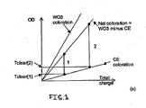
- FIG. 1 provides an illustration of coloration in an electrochromic device having a cathodic counter electrode layer.
- the overall dynamic range for such a device is given by the net optical density change upon transferring charge from the counter electrode to the electromatic material layer.
- Such a transfer of charge results in a loss of optical density from the counter electrode and a gain of optical density in the electrochromic material layer.
- the net change in optical density is given by the difference in electrochromic efficiency between the electrochromic material layer and the counter electrode.
- Condition 1 shows a lower overall level of charge and, thus, a lower initial bleached state as compared with Condition 2.
- Condition 2 shows the situation when the charge capacity is increased, such as by increasing the thickness of the counter electrode layer.
- electrochromic coatings and in particular electrochromic coatings that comprise solid state, inorganic thin films, and metal oxide thin films.
- electrochromic coatings that incorporate complementary anodic and cathodic electrochromic ion insertion layers, whose counter ions are either protons or lithium ions.
- electrochromic coatings that incorporate complementary anodic and cathodic electrochromic ion insertion layers, whose counter ions are either protons or lithium ions.
- electrochromic coatings that incorporate complementary anodic and cathodic electrochromic ion insertion layers, whose counter ions are either protons or lithium ions.
- improved methods for making complementary electrochromic layers to act as a counter electrode having improved properties over existing practices.
- an electrochromic device with a suitably wide transmission range between fully colored and fully bleached states, with suitably fast coloration and bleaching rates, and with suitable longevity and durability for outdoor architectural applications.
- an electrochromic device utilizing an anodic counter electrode comprised of a mixed tungsten-nickel oxide provides a suitably wide transmission range between the fully colored and fully bleached states. Moreover, such a device has found to be capable of reversibly intercalating several tens of millicoulombs per square centimeter of charge in the form of ions and charge compensating electrons. Further, applicants have discovered that an anodic counter electrode comprised of a mixed tungsten-nickel oxide provides a complementary response upon insertion of charge. Finally, applicants have discovered that an electrochromic device employing such a mixed tungsten-nickel oxide has improved transmission in the lithiated counter electrode layer when such device is heated.
- FIG. 1 is a graph detailing the coloration of an electrochromic device having a cathodic counter electrode layer.
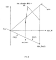
- FIG. 2 is a graph detailing the coloration of an electrochromic device having an anodic counter electrode layer.
- FIG. 3 is a schematic cross-section of a five layer electrochromic device in accordance with one embodiment of the current invention.
- FIG. 4 is a graph detailing the transmission level of a partially completed electrochromic device during the deposition of lithium into the anodic counter electrode.
- One object of the present invention is to provide an electrochromic device having an anodic complementary counter electrode which provides a high transmission in the fully intercalated state and is capable of long term stability suitable for use as a commercial product.
- an electrochromic device utilizing an anodic complementary counter electrode comprised of a mixed tugsten-nickel oxide which is capable of reversibly intercalating several tens of millicoulombs of charge per square centimeter, in the form of lithium ions and charge compensating electrons, and that upon intercalation of such ions, results in a high transmission in the fully intercalated state.
- Another objective of the present invention is to provide a method of preparing an anodic complementary counter electrode layer for use in connection with an electrochromic device comprising a mixed tungsten-nickel oxide.
- Another objective of the present invention is to provide a method of preparing an electrochromic device comprising an anodic complementary counter electrode comprised of a mixed tungsten-nickel oxide.
- anodic complementary counter electrode as described herein.
- the dynamic range of an electrochromic device employing such an anodic complementary counter electrode allows the device's dynamic range to be increased simply by increasing the amount of charge transferred, provided the amount of charge in the counter electrode is controlled well enough to maintain high transparency.
- FIG. 2 illustrates the coloration of an electrochromic device utilizing an anodic complementary counter electrode layer having an increased dynamic range and a high initial bleached state in comparison to a cathodic counter electrode.
- the dynamic range in FIG. 2 is given by the sum of the electrochromic efficiencies of the counter electrode and the electrochromic material layers. The net result is that the dynamic range may be increased simply by increasing the amount of charge transferred to the anodic complementary counter electrode layer.
- Condition 1 and Condition 2 are different in that the anodic counter electrode in Condition 1 holds a lower amount of charge as compared with the anodic counter electrode in Condition 2. However, the lower amount of charge in Condition 1 as compared with Condition 2 does not lead to a compromise in the bleached state optical density.
- Increasing the thickness of the anodic counter electrode, as demonstrated by Condition 2 increases the overall dynamic range of the device without changing the initial bleached state optical density.
- bleached state means the state of an electrochromic material that is at least partially clear or at least partially non-colored.
- intercalation means the reversible insertion of a molecule, atom or ion into a crystal lattice.
- lithium means elemental lithium, its salts, oxides, coordination complexes, and chelates. "Lithium” may also refer to lithium ions.
- sputtering means a physical process whereby atoms in a solid target material are ejected into the gas plasma phase due to bombardment of the material by energetic ions. "Sputtering” will be discussed with regard to its use in film deposition.
- FIG. 3 shows a five layer electrochromic device in cross-section.
- an electrochromic layer (“EC") 30 which produces a change in absorption or reflection upon oxidation or reduction
- an ion conductor layer (“IC") 32 which serves as an electrolyte, allowing the passage of ions while blocking electronic current
- a counter electrode (CE) 28 which serves as a storage layer for ions when the device is in the bleached state
- two conductive layers ("CL”) 24 and 26 which serve to apply an electrical potential to the electrochromic device.
- EC electrochromic layer
- IC ion conductor layer
- CE counter electrode
- CL conductive layers
- a low voltage electrical source 22 is connected to the device by means of conductive wires.
- an electrical potential be applied across the layered structure.
- the polarity of the electrical source will govern the nature of the electrical potential created and, thus, the direction of ion and electron flow.
- the electrical potential created will cause ions to flow from the counter electrode layer 28 through the ion conductor layer 32 to the electrochromic layer 30, thereby causing the electrochromic layer 30 to transform to the colored state thereby causing the transparency of the window 20 to be reduced.
- conductive layer materials include coatings of indium oxide, indium tin oxide, doped indium oxide, tin oxide, doped tin oxide, zinc oxide, doped zinc oxide, ruthenium oxide, doped ruthenium oxide and the like, as well as all thin metallic coatings that are substantially transparent, such as transition metals including gold, silver, aluminum, nickel alloy, and the like. It is also possible to employ multiple layer coatings, such as those available from Pilkington under the tradename of TEC-Glass®, or those available from PPG Industries under the tradenames SUNGATE® 300 and SUNGATE® 500.
- the conductive layers 24 and 26 may also be composite conductors prepared by placing highly conductive ceramic and metal wires or conductive layer patterns on one of the faces of the substrate and then overcoating this with transparent conductive materials such as indium tin oxide or doped tin oxides.
- the conductive layers may be further treated with appropriate anti-reflective or protective oxide or nitride layers.
- the material selected for use in conductive layer 26 is the same as the material selected for use in conductive layer 24. In other embodiments, the material selected for use in conductive layer 26 is different than the material selected for use in conductive layer 24.
- the conductive layers utilized in the present invention are transparent layers of indium tin oxide.
- the conductive layer 26 is disposed on a substrate having suitable optical, electrical, thermal, and mechanical properties such as, for example, glass, plastic or mirror materials, as a coating having a thickness in the range of about 5 nm to about 10,000 nm, and preferably about 10 nm to about 1,000 nm.
- suitable optical, electrical, thermal, and mechanical properties such as, for example, glass, plastic or mirror materials
- any thickness of the conductive layer may be employed that provides adequate conductance for the electrochromic device and which does not appreciably interfere with the transmission of light where required.
- conductive layer 24 is typically the final layer of the electrochromic device deposited on the counter electrode layer 28.
- Other passive layers used for improving optical properties, or providing moisture or scratch resistance may be deposited on top of the active layers. These conductive layers are connected to an electrical power source in a conventional manner.
- the electrochromic layer 30 employed as part of the present invention is well known to those skilled in the art.
- the electrochromic layer may be comprised of materials including inorganic, organic blends and/or composites of inorganic and organic electrochemically active materials such that the EC layer is capable of receiving ions transferred from the CE layer 28.
- Exemplary inorganic metal oxide electrochemically active materials include WO 3 , V 2 O 5 , MoO 3 , Nb 2 O 5 , TiO 2 , CuO, Ni 2 O 3 , Ir 2 O 3 , Cr 2 O 3 , Co 2 O 3 , Mn 2 O 3 , mixed oxides (e.g W-Mo oxide, W-V oxide) and the like.
- each of the aforementioned metal oxides may be appropriately doped with lithium, sodium, potassium, molybdenum, vanadium, titanium, and/or other suitable metals or compounds containing metals.
- the EC layer 30 is selected from WO 3 or doped WO 3 .
- the thickness of the EC layer 30 may vary depending on the electrochemically active material chosen. However, the EC layer 30 typically ranges from about 500 Angstroms to about 20,000 Angstroms in thickness, preferably from about 3400 Angstroms to about 4200 Angstroms.
- the ion conductor layer 32 employed as part of the present invention is comprised of a solid electrolyte capable of allowing ions to migrate through the layer.
- the ion conductor layer 32 must have a sufficient ionic transport property to allow ions, preferably lithium ions, to migrate through. Any material may be used for an ion conductor provided it allows for the passage of ions from the counter electrode layer 28 to the electrochromic layer 30.
- the ion conductor layer comprises a silicate-based structure.
- suitable ion conductors particularly adapted for lithium ion transmission include, but are not limited to, lithium silicate, lithium aluminum silicate, lithium aluminum borate, lithium borate, lithium zirconium silicate, lithium niobate, lithium borosilicate, lithium phosphosilicate, lithium nitride, lithium aluminum fluoride, and other such lithium-based ceramic materials, silicas, or silicon oxides.
- Other suitable ion-conducting materials can be used, such as silicon dioxide or tantalum oxide.
- the ion conductive layer 32 has low or no electronic conductivity.
- the preferred ion conductor material is a lithium-silicon-oxide produced by either sputtering or a sol-gel process.
- the thickness of the IC layer 32 may vary depending on the material. However, the IC layer 32 typically ranges from about 100 Angstroms to about 700 Angstroms in thickness, preferably from about 200 Angstroms to about 600 Angstroms in thickness, and most preferably from about 325 Angstroms to about 475 Angstroms in thickness.
- the counter electrode layer 28 utilized in the electrochromic device of the present invention is an anodic complementary counter electrode.
- the counter electrode layer 28 is considered anodic because it is anodically electrochromic, meaning that it will become more transparent when reduced (i.e. when ions are intercalated), which is the opposite of more common electrochromic materials such as tungsten oxides.
- the counter electrode 28 may act as a complementary electrochromic layer, causing the electrochromic device to color both from oxidation of the counter electrode and reduction of the electrochromic layer 28.
- charge in the form of ions and electrons
- the complementary counter electrode layer 28 of the present invention is comprised of a mixed tungsten-nickel oxide capable of storing ions and then releasing these ions for transfer to the electrochromic layer 30 in response to an appropriate electrical potential.
- the mixed oxide has the form of a Ni 2 O 3 and WO 3 composite.
- the amount of nickel present in the mixed tungsten-nickel oxide ranges from about 15% to about 90% by weight of said mixed tungsten-nickel oxide, preferably from about 30% to about 70% by weight of said tungsten-nickel oxide, and most preferably from about 40% to about 60% by weight of said tungsten-nickel oxide.
- the CE layer 28 will turn from a transparent state to a brown colored state.
- the mixed tungsten-nickel oxide is present in a crystalline state. In other embodiments, the mixed tungsten-nickel oxide may be present in a mixed amorphous and crystalline state. However, in preferred embodiments, the mixed tungsten-nickel oxide is present substantially in crystalline form.
- separate domains of different crystalline metal oxides may be present as an admixture (i.e. an admixture of crystalline tungsten oxide and crystalline nickel oxide).
- separate domains of a crystalline metal oxide and an amorphous metal oxide may be present (e.g. an admixture of amorphous nickel oxide and crystalline tungsten oxide, or an admixture of amorphous tungsten oxide and crystalline nickel oxide).
- the thickness of the complementary counter electrode layer 28 is variable depending on the application sought for the electrochromic device and the transmission range desired. As such, the thickness may range from about 500 Angstroms to about 6500 Angstroms. In one embodiment of the present invention, the thickness ranges from about 1500 Angstroms to about 2500 Angstroms, preferably ranging from about 1750 Angstroms to about 2050 Angstroms in thickness.
- the complementary counter electrode layer 28 of the present invention is also comprised of lithium.
- the lithium comprising the CE 28 is at least partially intercalated within the mixed tungsten-nickel oxide.
- the lithium is present as a film at least partially coating the surface of the CE.
- the lithium present in the CE 28, either on the CE surface and/or intercalated within the mixed tugsten-nickel oxide, is capable of being reversibly transferred from the CE to the EC 30 when an electrical potential is applied.
- the substrate 34 of the electrochromic device is comprised of transparent glass or plastic such as, for example, acrylic, polystyrene, polycarbonate, allyl diglycol carbonate [CR39 available from PPG Industries, Pittsburgh, Pa.], SAN [styrene acrylonitrile copolymer], poly(4-methyl-1-pentene), polyester, polyamide, etc.
- transparent glass or plastic such as acrylic, polystyrene, polycarbonate, allyl diglycol carbonate [CR39 available from PPG Industries, Pittsburgh, Pa.], SAN [styrene acrylonitrile copolymer], poly(4-methyl-1-pentene), polyester, polyamide, etc.
- the transparent substrate 34 it is preferably abrasion protected and barrier protected using a hard coat of, for example, a silica/silicone anti-abrasion coating, a diamond-like protection coating or their like, such as is well known in the plastic glazing art.
- the substrates have a thickness in the range of about 0.
- the complementary counter electrode layer 28 and the electrochromic layer 30 may be reversed in the overall structure of FIG. 3 .
- the polarity of the applied potential must be adjusted to ensure that the correct polarity for the layers is maintained.
- the completed device of FIG. 3 is subjected to a heat treatment process, carried out subsequent to the fabrication of the device.
- a device subjected to such treatment has improved conductivity, an increased conductive layer transparency, and an increased transmission of the lithiated CE layer.
- the lithiated mixed tungsten-nickel oxide may transform into a composite of Li 2 WO 4 and Ni 2 O 3 .
- the electrochromic device described herein could be coupled with radiation sensors (e.g., visible and solar) and energy management systems to automatically control their transmission and reflection.
- radiation sensors e.g., visible and solar
- the electrochromic device of the present invention may be powered with solar cells, thermoelectric sources, wind generators, etc., to make them self-sustaining. These may be also coupled into charge storage devices such as batteries, re-chargeable batteries, capacitors or other means. The charge storage devices could be utilized as automatic backup power source when primary source of power is interrupted.
- the electrochromic device of the present invention may also be used as filters in displays or monitors for reducing the ambient light intensity, e.g., sun glare, that is incident on the monitor or display surface.
- the device may be employed to enhance the image quality of displays and monitors, particularly in well lit conditions.
- the electrochromic device of the present invention may also be used as eyewear or sunglasses.
- a method of preparing an electrochromic device employing an anodic complementary counter electrode is also provided.
- a first conductive layer 26 is deposited on substrate 34 by methods known in the art and in accordance with the desired properties of a conductor layer as previously mentioned.
- An electrochromic layer 30 is then deposited on conductor layer 26 through wet chemical methods, chemical vapor deposition and/or physical vapor deposition (e.g. sol-gel, metallo-organic decomposition, laser ablation, evaporation, e-beam assisted evaporation, sputtering, intermediate frequency reactive sputtering, RF sputtering, magnetic sputtering, DC sputtering, PVD and CVD and the like).
- the electrochromic layer 30 is deposited via intermediate frequency reactive sputtering or DC sputtering techniques.
- the EC layer 30 is deposited on a heated first conductor layer 26.
- the deposited electrochromic layer 30 may be comprised of metal oxides including titanium oxides, vanadium oxides, tungsten oxides, molybdenum oxides, or doped variants thereof.
- the electrochromic layer 30 deposited is comprised of WO 3 .
- the deposited WO 3 may contain a stoichiometric excess or deficiency of oxygen, depending on the deposition method and conditions chosen.
- the WO 3 may be doped with an appropriate metal or metallic compound.
- An ion conductor layer 32 is then deposited on EC layer 30 through wet chemical methods, chemical vapor deposition and/or physical vapor deposition (e.g. sol-gel, metallo-organic decomposition, laser ablation, evaporation, e-beam assisted evaporation, sputtering, intermediate frequency reactive sputtering, RF sputtering, magnetic sputtering, DC sputtering, PVD and CVD and the like).
- the ion conductor layer is deposited via a sol gel method or reactive sputtering.
- An anodic complementary counter electrode layer 28 comprised of a film of a mixed tungsten-nickel oxide is then deposited on the IC layer 32 through physical vapor deposition, intermediate frequency reactive sputtering, DC sputtering, or RF-magnetron sputtering.
- tungsten chips are placed on a nickel target with the sputtering pressure set between 1mTorr and 10mTorr by introducing oxygen or argon into the chamber.
- powdered tungsten-nickel metals or oxides are hot pressed or hot isostatically pressed (HIPed) and utilized as a sputtering target in an oxygen rich or argon rich atmosphere.
- the tungsten-nickel oxide film is reduced through the deposition of lithium.
- the deposition of the lithium is achieved through one of either wet chemical methods, sol-gel, chemical vapor deposition, physical vapor deposition, or reactive sputtering.
- the source of the lithium deposited on the tungsten-nickel oxide film is lithium metal deposited in vacuum using a non-reactive sputtering process.
- the amount of lithium deposited on the mixed tungsten-nickel oxide film is carefully controlled such that an amount of lithium is added that allows for the greatest transmission of light through the counter electrode layer 28, and hence the whole device.
- Typical results for the optical measurements of the electrochromic device are shown in FIG. 4 , where the measured transmission is plotted as a function of the amount of intercalated lithium.
- the percent transmission which is dominated by the absorption of the counter electrode, starts out low and increases as the charge, in the form of lithium ions, is intercalated.
- the transmission proceeds through a maximum and then begins to decrease when additional lithium is added beyond the maximum.
- the amount of charge necessary to obtain the maximum transmission of the device, measured in-situ is utilized as a process control parameter to ensure the correct level of lithium is deposited, and ultimately intercalated onto or into the mixed tungsten-nickel oxide film.
- the starting transmission for the counter electrode depends on the thickness of the mixed tungsten-nickel oxide film and the absorption coefficient, which is dependent on the tungsten-nickel ratio and the oxidation state of the material. Moreover, it has been shown that a higher transmission is obtained for a more tungsten rich film and also for a more reduced film.
- the amount of lithium deposited onto the counter electrode layer 28 is in excess of the amount required to achieve the maximum transmission, such that the greatest transmission is still achieved as and when the excess lithium is lost during subsequent processing steps. If excess lithium is deposited, such amount of excess lithium ranges from about 10% to about 40% above that required to achieve the maximum transmission. The amount of excess lithium added, however, ultimately depends on the CE layer 28 thickness and the requirements for the electrochromic device's performance.
- a second conductive layer 24 is deposited on the lithiated CE layer 28 by methods well known in the art and as described above in the deposition of the first conductive layer 26.
- the device is completed by heating the entire electrochromic device in a vacuum, an inert atmosphere, or an atmospheric oven. It has been determined that in order to obtain a suitably uniform device after processing, there is a trade-off between the heating time and the size, e.g. larger windows require a longer time to heat up. It is also observed that the process can be achieved by heating at a lower temperature for a shorter time. In other words, there appears to be a requirement that the time-temperature product is approximately constant. Devices with sizes suitable for use in glazing products should be heated to a temperature ranging from about 280°C to about 500°C, preferably to a temperature ranging from about 355°C to about 395°C.
- the device may be heated for a time ranging from about 1 minute to about 120 minutes, preferably from about 10 minutes to about 30 minutes. Smaller devices, for other applications such as variable transmission filters for cameras and the like, can be heated much more rapidly, as the stringent requirements for uniformity are somewhat reduced.
- the device can be heated prior to the second conductive layers being deposited.
- This method results in electrochromic device properties substantially the same as those discussed in the preceding embodiment, but allows for the heating to be done in the same process chamber as the deposition, possibly resulting in improved process flow.
- the heat treatment process has a positive effect on the switching characteristics of the electrochromic device, as well as improving the conductivity and transparency of the second conductive layer 26.
- the heat treatment also has the effect of increasing the transmission of the lithiated CE layer 28.
- the position of the complementary counter electrode layer 28 and the electrochromic layer 30 may be reversed in the overall structure presented in FIG. 3 .
- the method of manufacturing the device does not change with regard to the steps that have to be performed to generate each layer. Regardless of the order of steps performed to form an electrochromic device employing the aforementioned complementary counter electrode, the device may still be subjected to the heat treatment process described herein.
- a complementary counter electrode comprised of a mixed tungsten-nickel oxide may be used to develop a counter electrode for use in connection with any electrochromic device. That is, the methods used to develop the complementary counter electrode are not limited to use in the specific electrochromic device discussed herein. Moreover, the method of making the complementary counter electrode discussed above may also be used to deposit a complementary counter electrode on any surface, not merely ion conductor layers or other conductive layers.
Landscapes
- Physics & Mathematics (AREA)
- Nonlinear Science (AREA)
- General Physics & Mathematics (AREA)
- Optics & Photonics (AREA)
- Chemical & Material Sciences (AREA)
- Inorganic Chemistry (AREA)
- Crystallography & Structural Chemistry (AREA)
- Electrochromic Elements, Electrophoresis, Or Variable Reflection Or Absorption Elements (AREA)
Claims (33)
- Dispositif électrochromique pour traitement thermique comprenant :a) une première électrode comprenant une couche électrochromique cathodique (30) ou une couche de contre-électrode anodique (28),b) une seconde électrode comprenant une autre dite couche électrochromique ou ladite couche de contre-électrode anodique,c) une couche conductrice d'ions (32) pour conduire des ions entre lesdites première et seconde électrodes,d) une première couche conductrice (24), ete) une seconde couche conductrice (26),lesdites première et seconde électrodes (28, 30) et ladite couche conductrice d'ions (32) étant moisées entre lesdites première et seconde couches conductrices (24, 26), et
ladite couche de contre-électrode anodique (28) comprenant un oxyde mixte tungstène-nickel sous forme cristalline et le lithium. - Dispositif électrochromique selon la revendication 1, dans lequel une quantité de nickel dudit oxyde mixte tungstène-nickel pèse environ entre 15% et 90% du poids dudit oxyde de tungstène et de nickel mixte.
- Dispositif électrochromique selon la revendication 2, dans lequel ladite quantité varie d'environ 30% à 70% du poids dudit oxyde mixte tungstène-nickel.
- Dispositif électrochromique selon la revendication 2, dans lequel ladite quantité varie d'environ 40% à 60% du poids dudit oxyde mixte tungstène-nickel.
- Dispositif électrochromique selon la revendication 1, dans lequel ladite couche électrochromique cathodique (30) comprend un oxyde métallique.
- Dispositif électrochromique selon la revendication 5, dans lequel ledit oxyde métallique est choisi dans le groupe constitué par l'oxyde de tungstène, l'oxyde de vanadium, l'oxyde de molybdène, l'oxyde de niobium, l'oxyde de titane, l'oxyde de cuivre, l'oxyde d'iridium, l'oxyde de chrome, et l'oxyde de manganèse.
- Dispositif électrochromique selon la revendication 5, dans lequel ledit oxyde métallique est dopé par un ou plusieurs métaux.
- Dispositif électrochromique selon la revendication 1, dans lequel lesdites première et seconde couches conductrices (24, 26) comprennent un oxyde métallique.
- Dispositif électrochromique selon la revendication 8, dans lequel ledit oxyde métallique est choisi dans le groupe constitué par l'oxyde d'indium, l'oxyde d'étain, l'oxyde de zinc et l'oxyde de ruthénium.
- Dispositif électrochromique selon la revendication 8, dans lequel ledit oxyde métallique est dopé par un ou plusieurs métaux.
- Dispositif électrochromique selon la revendication 8, dans lequel lesdites couches conductrices (24, 26) comprennent le même oxyde métallique.
- Dispositif électrochromique selon la revendication 8, dans lequel lesdites couches conductrices (24, 26) comprennent différents oxydes métallique.
- Dispositif électrochromique selon la revendication 1, dans lequel lesdites première et seconde couches conductrices (24, 26) comportent un revêtement sensiblement transparent d'un métal de transition.
- Dispositif électrochromique selon la revendication 1, dans lequel ladite couche conductrice d'ions (32) comprend une couche conductrice de lithium-ion.
- Dispositif électrochromique selon la revendication 14, dans lequel ladite couche conductrice de lithium-ion (32) comprend un matériau choisi dans le groupe constitué de silicates, d'oxydes de silicium, et des borates.
- Dispositif électrochromique selon la revendication 1, disposé sur un substrat (34) choisi dans le groupe constitué de verre ou de plastique.
- Le dispositif électrochromique selon la revendication 1, dans lequel ladite contre-électrode anodique (28) a une épaisseur sensiblement uniforme comprise entre environ 500 Angströms et 6500 Angströms.
- Dispositif électrochromique selon la revendication 17, dans lequel ladite épaisseur est comprise entre environ 1500 et 2500 angströms.
- Procédé de préparation d'un dispositif électrochromique comprenant:a) la fourniture d'une première couche conductrice (26),b) le dépôt d'une couche cathodique électrochromique (30) ou d'une couche de contre-électrode anodique (28) comprenant un oxyde mixte tungstène-nickel sur ladite première couche conductrice (26), fournissant ainsi une première électrode déposée,c) le dépôt d'une couche conductrice d'ions (32) sur ladite première électrode déposée,d) le dépôt de l'autre dite couche électrochromique cathodique ou de ladite couche de contre-électrode anodique sur ladite couche conductrice d'ion, fournissant ainsi une seconde électrode déposée,e) le dépôt d'une seconde couche conductrice (24) sur ladite deuxième électrode déposée,f) le dépôt de lithium sur la couche de contre-électrode (28) de sorte que ledit oxyde mixte tungstène-nickel soit réduit, quand une quantité dudit lithium déposée est supérieure à une quantité qui fournit une transmission maximum à travers ladite couche de contre-électrode, dans laquelle ladite couche de contre-électrode comprend un oxyde mixte tungstène-nickel à l'état cristallin et du lithium, etg) le chauffage dudit dispositif électrochromique après le dépôt de ladite électrode déposée ou après le dépôt de ladite seconde couche conductrice.
- Procédé selon la revendication 19, dans lequel une quantité d'oxyde mixte tungstène-nickel varie entre environ 15% à 90% du poids dudit oxyde mixte.
- Procédé selon la revendication 20, dans lequel ladite quantité varie d'environ 30% à 70% du poids dudit oxyde mixte.
- Procédé selon la revendication 20, dans lequel ladite quantité varie d'environ 40% à 60% du poids dudit oxyde mixte.
- Procédé selon la revendication 19, dans lequel ladite couche électrochromique (30) comprend un oxyde métallique.
- Procédé selon la revendication 23, dans lequel ledit oxyde métallique est choisi dans le groupe constitué par l'oxyde de tungstène, l'oxyde de vanadium, l'oxyde de molybdène, l'oxyde de niobium, l'oxyde de titane, l'oxyde d'iridium, l'oxyde de chrome, oxyde de cuivre, et l'oxyde de manganèse.
- Procédé selon la revendication 23, dans lequel ledit oxyde métallique est dopé par un ou plusieurs métaux.
- Procédé selon la revendication 19, dans lequel ladite quantité en excès varie d'environ 10% à 40% au-dessus de ladite quantité qui permet une transmission maximale à travers ladite couche de contre-électrode (28).
- Procédé selon la revendication 19, comprenant le chauffage dudit dispositif électrochromique à une température comprise entre environ 280°C et 500°C.
- Procédé selon la revendication 27, comprenant le chauffage dudit dispositif électrochromique à une température comprise entre environ 355°C à 395°C.
- Procédé selon la revendication 27, comprenant le dépôt de ladite couche de contre-électrode (28) au moyen d'un dépôt physique en phase vapeur.
- Procédé selon la revendication 19, comprenant le dépôt de ladite couche de contre-électrode (28) au moyen d'une pulvérisation réactive à fréquence intermédiaire.
- Procédé selon la revendication 19, comprenant le dépôt de ladite couche de contre-électrode (28) au moyen de pulvérisation DC.
- Procédé selon la revendication 19, comprenant le dépôt dudit lithium sur ladite couche de contre-électrode (28) au moyen de procédés chimiques par voie humide.
- Procédé selon la revendication 19, comprenant le dépôt dudit lithium sur ladite couche de contre-électrode (28) au moyen d'un dépôt physique en phase vapeur.
Applications Claiming Priority (1)
| Application Number | Priority Date | Filing Date | Title |
|---|---|---|---|
| US65557805P | 2005-02-23 | 2005-02-23 |
Publications (2)
| Publication Number | Publication Date |
|---|---|
| EP1696261A1 EP1696261A1 (fr) | 2006-08-30 |
| EP1696261B1 true EP1696261B1 (fr) | 2013-10-09 |
Family
ID=36218512
Family Applications (1)
| Application Number | Title | Priority Date | Filing Date |
|---|---|---|---|
| EP06003692.8A Expired - Lifetime EP1696261B1 (fr) | 2005-02-23 | 2006-02-23 | Procédés de réalisation de couches de contre-électrode pour dispositifs électrochimiques |
Country Status (4)
| Country | Link |
|---|---|
| US (5) | US7372610B2 (fr) |
| EP (1) | EP1696261B1 (fr) |
| JP (1) | JP4866100B2 (fr) |
| ES (1) | ES2434030T3 (fr) |
Cited By (1)
| Publication number | Priority date | Publication date | Assignee | Title |
|---|---|---|---|---|
| US9429809B2 (en) | 2009-03-31 | 2016-08-30 | View, Inc. | Fabrication of low defectivity electrochromic devices |
Families Citing this family (162)
| Publication number | Priority date | Publication date | Assignee | Title |
|---|---|---|---|---|
| JP2005309137A (ja) * | 2004-04-22 | 2005-11-04 | Tokai Rika Co Ltd | 反射率可変ミラー |
| US7372610B2 (en) | 2005-02-23 | 2008-05-13 | Sage Electrochromics, Inc. | Electrochromic devices and methods |
| US7265891B1 (en) * | 2006-06-20 | 2007-09-04 | Eclipse Energy Systems | Electrochromic device with self-forming ion transfer layer and lithium-fluoro-nitride electrolyte |
| EP2089764B1 (fr) * | 2006-11-09 | 2016-01-06 | Sage Electrochromics, Inc. | Procédé permettant de fabriquer un dispositif de commutation des ions sans étape de lithiation distincte |
| EP2165238A4 (fr) * | 2007-06-01 | 2011-04-06 | Chromogenics Ab | Commande d'un dispositif électrochromique |
| JP2009008751A (ja) * | 2007-06-26 | 2009-01-15 | Tokai Rika Co Ltd | エレクトロクロミックミラー |
| JP4949136B2 (ja) * | 2007-06-26 | 2012-06-06 | 株式会社東海理化電機製作所 | エレクトロクロミックミラー |
| JP2009008750A (ja) * | 2007-06-26 | 2009-01-15 | Tokai Rika Co Ltd | エレクトロクロミックミラー |
| JP2009008749A (ja) * | 2007-06-26 | 2009-01-15 | Tokai Rika Co Ltd | エレクトロクロミックミラー |
| JP4972001B2 (ja) * | 2008-01-23 | 2012-07-11 | 株式会社東海理化電機製作所 | エレクトロクロミックミラー |
| US9782949B2 (en) | 2008-05-30 | 2017-10-10 | Corning Incorporated | Glass laminated articles and layered articles |
| US8514476B2 (en) | 2008-06-25 | 2013-08-20 | View, Inc. | Multi-pane dynamic window and method for making same |
| US7961375B2 (en) * | 2008-06-25 | 2011-06-14 | Soladigm, Inc. | Multi-cell solid-state electrochromic device |
| US8842357B2 (en) | 2008-12-31 | 2014-09-23 | View, Inc. | Electrochromic device and method for making electrochromic device |
| US10156762B2 (en) | 2009-03-31 | 2018-12-18 | View, Inc. | Counter electrode for electrochromic devices |
| US9723723B2 (en) | 2009-03-31 | 2017-08-01 | View, Inc. | Temperable electrochromic devices |
| US11599003B2 (en) | 2011-09-30 | 2023-03-07 | View, Inc. | Fabrication of electrochromic devices |
| US8582193B2 (en) | 2010-04-30 | 2013-11-12 | View, Inc. | Electrochromic devices |
| US8764951B2 (en) | 2010-04-30 | 2014-07-01 | View, Inc. | Electrochromic devices |
| US9007674B2 (en) | 2011-09-30 | 2015-04-14 | View, Inc. | Defect-mitigation layers in electrochromic devices |
| US10852613B2 (en) | 2009-03-31 | 2020-12-01 | View, Inc. | Counter electrode material for electrochromic devices |
| US10591795B2 (en) | 2009-03-31 | 2020-03-17 | View, Inc. | Counter electrode for electrochromic devices |
| US8300298B2 (en) | 2010-04-30 | 2012-10-30 | Soladigm, Inc. | Electrochromic devices |
| US8764950B2 (en) | 2010-04-30 | 2014-07-01 | View, Inc. | Electrochromic devices |
| US12043890B2 (en) | 2009-03-31 | 2024-07-23 | View, Inc. | Electrochromic devices |
| US10261381B2 (en) | 2009-03-31 | 2019-04-16 | View, Inc. | Fabrication of low defectivity electrochromic devices |
| US11187954B2 (en) | 2009-03-31 | 2021-11-30 | View, Inc. | Electrochromic cathode materials |
| US9261751B2 (en) | 2010-04-30 | 2016-02-16 | View, Inc. | Electrochromic devices |
| FR2948356B1 (fr) | 2009-07-22 | 2011-08-19 | Saint Gobain | Dispositif electrochrome |
| US10303035B2 (en) * | 2009-12-22 | 2019-05-28 | View, Inc. | Self-contained EC IGU |
| US12353109B2 (en) | 2009-12-22 | 2025-07-08 | View Operating Corporation | Electrochromic cathode materials |
| KR101097856B1 (ko) * | 2010-03-04 | 2011-12-23 | 서울대학교산학협력단 | 전기 변색 소자 제조방법 |
| ES2450520T5 (es) | 2010-03-05 | 2017-08-07 | Sage Electrochromics, Inc. | Laminado de un dispositivo electrocrómico a sustratos de vidrio |
| US8493646B2 (en) | 2010-04-22 | 2013-07-23 | Sage Electrochromics, Inc. | Series connected electrochromic devices |
| US8228587B2 (en) | 2010-04-22 | 2012-07-24 | Sage Electrochromics, Inc. | Series connected electrochromic devices |
| CN102934009B (zh) * | 2010-04-30 | 2016-10-19 | 唯景公司 | 电致变色器件 |
| US9759975B2 (en) | 2010-04-30 | 2017-09-12 | View, Inc. | Electrochromic devices |
| WO2011137104A1 (fr) * | 2010-04-30 | 2011-11-03 | Soladigm, Inc. | Dispositifs électro-chromatiques |
| FR2961609B1 (fr) | 2010-06-21 | 2012-06-01 | Saint Gobain | Dispositif a proprietes optiques et/ou energetiques electrocommandables |
| FR2962818B1 (fr) | 2010-07-13 | 2013-03-08 | Saint Gobain | Dispositif electrochimique a proprietes de transmission optique et/ou energetique electrocommandables. |
| FR2962682B1 (fr) | 2010-07-16 | 2015-02-27 | Saint Gobain | Vitrage electrochimique a proprietes optiques et/ou energetiques electrocommandables |
| US8270059B2 (en) * | 2010-08-05 | 2012-09-18 | Soladigm, Inc. | Multi-pane electrochromic windows |
| US12496809B2 (en) | 2010-11-08 | 2025-12-16 | View Operating Corporation | Electrochromic window fabrication methods |
| US9958750B2 (en) | 2010-11-08 | 2018-05-01 | View, Inc. | Electrochromic window fabrication methods |
| US8717658B2 (en) | 2011-02-09 | 2014-05-06 | Kinestral Technologies, Inc. | Electrochromic multi-layer devices with spatially coordinated switching |
| KR101453037B1 (ko) * | 2011-03-23 | 2014-10-21 | 주식회사 엘지화학 | 전극조립체 및 이의 제조방법 |
| JP2014510956A (ja) | 2011-03-31 | 2014-05-01 | セイジ・エレクトロクロミクス,インコーポレイテッド | 熱撮像を用いてエレクトロクロミックデバイス内の欠陥を検出及び修復するためのシステム及び方法 |
| CN103562431B (zh) * | 2011-04-07 | 2016-05-11 | Sage电致变色显示有限公司 | 用于控制锂均匀度的改善的方法 |
| US20120268803A1 (en) | 2011-04-20 | 2012-10-25 | Sage Electrochromics, Inc. | Electrochromic systems and controls comprising unique identifiers |
| JP2014519622A (ja) | 2011-05-26 | 2014-08-14 | セイジ・エレクトロクロミクス,インコーポレイテッド | エレクトロクロミック装置のための橋絡されたバスバー |
| US8430707B2 (en) | 2011-05-27 | 2013-04-30 | Sage Electrochromics, Inc. | Apparatus and method for repair of defects in an electronic energy control or display device |
| KR101988391B1 (ko) | 2011-06-27 | 2019-06-12 | 솔레라스 리미티드 | 스퍼터링 타겟 |
| US9217198B2 (en) | 2011-07-07 | 2015-12-22 | Itn Energy Systems, Inc. | Insertion of lithium into electrochromic devices after completion |
| CN107300819B (zh) * | 2011-07-21 | 2021-03-12 | Sage电致变色显示有限公司 | 同时掺杂有锂和金属掺杂物的电致变色的镍氧化物 |
| EP2766774B1 (fr) | 2011-10-10 | 2019-01-16 | Saint-Gobain Glass France | Vitrage isolant électrochrome doté d'un bouton de commande de capteur capacitif |
| WO2013082279A1 (fr) | 2011-11-29 | 2013-06-06 | Itn Energy Systems, Inc. | Système de revêtement modulaire à plusieurs zones |
| US10295880B2 (en) | 2011-12-12 | 2019-05-21 | View, Inc. | Narrow pre-deposition laser deletion |
| US12061402B2 (en) | 2011-12-12 | 2024-08-13 | View, Inc. | Narrow pre-deposition laser deletion |
| CA2859023C (fr) | 2011-12-12 | 2023-08-22 | View, Inc. | Dispositifs en couches minces et fabrication de ceux-ci |
| US10802371B2 (en) | 2011-12-12 | 2020-10-13 | View, Inc. | Thin-film devices and fabrication |
| US12403676B2 (en) | 2011-12-12 | 2025-09-02 | View Operating Corporation | Thin-film devices and fabrication |
| US11865632B2 (en) | 2011-12-12 | 2024-01-09 | View, Inc. | Thin-film devices and fabrication |
| US9293796B2 (en) | 2011-12-15 | 2016-03-22 | Itn Energy Systems, Inc. | Metal-air battery with dual electrode anode |
| US8980485B2 (en) | 2011-12-30 | 2015-03-17 | Itn Energy Systems, Inc. | Rechargeable, thin-film, all solid-state metal-air battery |
| US9281672B2 (en) | 2012-01-20 | 2016-03-08 | Sage Electrochromics, Inc. | Electrical connectivity within architectural glazing frame systems |
| US8976440B2 (en) | 2012-02-03 | 2015-03-10 | Itn Energy Systems, Inc. | Autonomous electrochromic assembly |
| US9013777B2 (en) | 2012-02-03 | 2015-04-21 | Itn Energy Systems, Inc. | Integrated device architectures for electrochromic devices |
| US20130222877A1 (en) | 2012-02-28 | 2013-08-29 | Sage Electrochromics, Inc. | Multi-zone electrochromic devices |
| US20130222878A1 (en) | 2012-02-28 | 2013-08-29 | Sage Electrochromics, Inc. | Multi-zone electrochromic devices |
| US12578609B2 (en) | 2012-03-13 | 2026-03-17 | View Operating Corporation | Methods of controlling multi-zone tintable windows |
| US11635666B2 (en) | 2012-03-13 | 2023-04-25 | View, Inc | Methods of controlling multi-zone tintable windows |
| US9341912B2 (en) | 2012-03-13 | 2016-05-17 | View, Inc. | Multi-zone EC windows |
| US12153320B2 (en) | 2012-03-13 | 2024-11-26 | View, Inc. | Multi-zone EC windows |
| US20140327950A1 (en) | 2012-03-26 | 2014-11-06 | Hpo Assets Llc | Electrochromic materials and optical systems employing the same |
| US20130293825A1 (en) * | 2012-03-26 | 2013-11-07 | Pixeloptics, Inc. | Electrochromic materials and optical systems employing the same |
| US20130258436A1 (en) | 2012-04-03 | 2013-10-03 | Sage Electrochromics, Inc. | Patterned obscuration lines for electrochromic devices |
| CN104661787A (zh) | 2012-04-05 | 2015-05-27 | Sage电致变色显示有限公司 | 用于电变色装置制造的热激光划线切割方法和设备及相应的切割玻璃面板 |
| CN104364707B (zh) * | 2012-05-02 | 2018-03-27 | 唯景公司 | 电致变色器件 |
| JP2015530339A (ja) | 2012-06-27 | 2015-10-15 | セイジ・エレクトロクロミクス,インコーポレイテッド | 絶縁グレージングユニットのための肩部スペーサキー |
| WO2014025921A1 (fr) | 2012-08-08 | 2014-02-13 | Kinestral Technologies, Inc. | Dispositifs multicouches électrochromiques avec structure de modulation de courant |
| WO2014025900A1 (fr) | 2012-08-08 | 2014-02-13 | Kinestral Technologies, Inc. | Dispositifs multicouches électrochromiques à couches électroconductrices composites |
| US9091868B2 (en) | 2012-08-08 | 2015-07-28 | Kinestral Technologies, Inc. | Electrochromic multi-layer devices with composite current modulating structure |
| EP3543781B1 (fr) * | 2012-08-09 | 2022-10-12 | SAGE Electrochromics, lnc. | Matériaux de type oxyde métallique de lithium pour dispositifs électrochromiques |
| US9618820B2 (en) | 2012-11-14 | 2017-04-11 | Solarwindow Technologies, Inc. | Integrated photovoltaic and electrochromic windows |
| US9158172B2 (en) | 2012-11-14 | 2015-10-13 | Sage Electrochromics, Inc. | Color matched coating for bus bars |
| TW201439371A (zh) * | 2013-01-21 | 2014-10-16 | Kinestral Technologies Inc | 多層電致變色結構之製備方法 |
| ES2733281T3 (es) | 2013-01-21 | 2019-11-28 | Kinestral Tech Inc | Dispositivo electrocromático multicapa con ánodo a base de óxido de litio y níquel |
| US9377663B2 (en) | 2013-01-21 | 2016-06-28 | Kinestral Technologies, Inc. | Electrochromic lithium nickel group 4 mixed metal oxides |
| US9013778B2 (en) | 2013-03-06 | 2015-04-21 | Sage Electrochromics, Inc. | Laser cuts to reduce electrical leakage |
| JP6285971B2 (ja) | 2013-03-08 | 2018-02-28 | セイジ・エレクトロクロミクス,インコーポレイテッド | 複数の独立して制御可能なゾーン及び内部バスバーを有するエレクトロクロミックデバイス |
| WO2014143410A1 (fr) * | 2013-03-15 | 2014-09-18 | Kinestral Technologies, Inc. | Oxydes métalliques mélangés de groupe 6-lithium-nickel électrochromiques |
| US9581741B1 (en) | 2013-05-31 | 2017-02-28 | Itn Energy Systems, Inc. | Infrared control coating of thin film devices |
| US9152001B2 (en) | 2013-07-25 | 2015-10-06 | Sage Electrochromics, Inc. | Electrochromic devices having improved structure for reducing current leakage across lower transparent conductor layers |
| US9606409B2 (en) | 2013-09-13 | 2017-03-28 | Itn Energy Systems Inc. | Electrochromic window insert assembly and methods of manufacture |
| US20150153622A1 (en) | 2013-12-03 | 2015-06-04 | Sage Electrochromics, Inc. | Methods for producing lower electrical isolation in electrochromic films |
| AT14157U1 (de) * | 2013-12-20 | 2015-05-15 | Plansee Se | W-Ni-Sputtertarget |
| US10044028B1 (en) | 2014-01-29 | 2018-08-07 | Itn Energy Systems, Inc. | Composite cathode solid state battery |
| US10767143B2 (en) | 2014-03-06 | 2020-09-08 | Sage Electrochromics, Inc. | Particle removal from electrochromic films using non-aqueous fluids |
| US11891327B2 (en) | 2014-05-02 | 2024-02-06 | View, Inc. | Fabrication of low defectivity electrochromic devices |
| JP6452734B2 (ja) | 2014-06-17 | 2019-01-16 | セイジ・エレクトロクロミクス,インコーポレイテッド | 耐湿性エレクトロクロミックデバイス |
| US10170654B2 (en) | 2014-06-25 | 2019-01-01 | Sage Electrochromics, Inc. | Solar powered device with scalable size and power capacity |
| US10859887B2 (en) * | 2015-09-18 | 2020-12-08 | View, Inc. | Power distribution networks for electrochromic devices |
| FR3023931B1 (fr) * | 2014-07-16 | 2016-07-08 | Commissariat Energie Atomique | Dispositif electrochrome |
| US10061177B2 (en) | 2014-07-23 | 2018-08-28 | Kinestral Technologies, Inc. | Process for preparing multi-layer electrochromic stacks |
| US10670936B2 (en) | 2014-07-23 | 2020-06-02 | Kinestral Technologies, Inc. | Wet-coating of thin film lithium nickel oxides for electrochromic applications |
| US10345671B2 (en) | 2014-09-05 | 2019-07-09 | View, Inc. | Counter electrode for electrochromic devices |
| US12235560B2 (en) | 2014-11-25 | 2025-02-25 | View, Inc. | Faster switching electrochromic devices |
| CN116789175A (zh) | 2014-11-26 | 2023-09-22 | 唯景公司 | 用于电致变色装置的对电极 |
| KR102755062B1 (ko) * | 2014-11-26 | 2025-01-14 | 뷰, 인크. | 전기변색 디바이스들을 위한 상대 전극 |
| FR3031197B1 (fr) * | 2014-12-31 | 2017-06-16 | Saint Gobain | Procede de traitement thermique rapide d'un empilement electrochrome tout solide complet |
| WO2016111918A1 (fr) | 2015-01-06 | 2016-07-14 | Sage Electrochromics, Inc. | Ensemble fenêtre et procédé afférent |
| JP6505864B2 (ja) | 2015-01-06 | 2019-04-24 | セイジ・エレクトロクロミクス,インコーポレイテッド | 一式の窓アセンブリ及びその製作方法 |
| CN107533267A (zh) | 2015-03-20 | 2018-01-02 | 唯景公司 | 更快速地切换低缺陷电致变色窗 |
| CN119916619A (zh) * | 2015-07-14 | 2025-05-02 | 唯景公司 | 用于电致变色装置的对电极 |
| US9858520B2 (en) * | 2015-09-21 | 2018-01-02 | Microsoft Technology Licensing, Llc | Controllable marking |
| CN105572987A (zh) * | 2015-12-22 | 2016-05-11 | 深圳市华星光电技术有限公司 | 液晶显示器以及用于使液晶显示器显示图象的驱动方法 |
| CA3014101A1 (fr) * | 2016-02-11 | 2017-08-17 | Basf Se | Dispositifs electrochromiques |
| WO2017184430A1 (fr) | 2016-04-19 | 2017-10-26 | Sage Electrochromics, Inc. | Dispositif électrochromique comprenant une couche d'oxyde conductrice transparente et une barre omnibus et son procédé de formation |
| WO2018119095A1 (fr) | 2016-12-22 | 2018-06-28 | Sage Electrochromics, Inc. | Appareil comprenant un dispositif électrochromique conçu pour maintenir un état de transmission à gradation continue |
| CN110337716A (zh) | 2017-02-27 | 2019-10-15 | Sage电致变色显示有限公司 | 包括基板和透明导电层的电气设备及形成电气设备的方法 |
| EP3610324B1 (fr) | 2017-04-12 | 2024-05-29 | Saint-Gobain Glass France | Structure électrochrome, et procédé de séparation d'une structure électrochrome |
| GB2562115B (en) | 2017-05-05 | 2022-02-16 | William Blythe Ltd | Tungsten oxide |
| GB2562116B (en) | 2017-05-05 | 2022-04-27 | William Blythe Ltd | Metal oxide, composition comprising the same and method of making metal oxide |
| WO2018207591A1 (fr) * | 2017-05-10 | 2018-11-15 | 国立研究開発法人物質・材料研究機構 | Dispositif électrochromique utilisant un polymère hybride organique/métallique et son procédé de production |
| CA3070511A1 (fr) | 2017-07-20 | 2019-01-24 | Click Materials Corp. | Photodeposition d'oxydes metalliques pour dispositifs electrochromes |
| EP3679423B1 (fr) * | 2017-09-08 | 2024-02-21 | Essilor International | Dispositif électrochrome durable comprenant un film d'oxyde de tungstène préparé dans un environnement de bombardement ionique élevé et de dépôt basse pression et ses procédés de fabrication |
| US11714327B2 (en) | 2017-09-12 | 2023-08-01 | Sage Electrochromics, Inc. | Non-light-emitting variable transmission device and a method of forming the same |
| EP3707104B1 (fr) | 2017-11-06 | 2024-05-15 | Sage Electrochromics, Inc. | Article comprenant un dispositif non électroluminescent à transmission variable et un revêtement |
| CN112470065B (zh) | 2018-07-31 | 2024-08-13 | Sage电致变色显示有限公司 | 电化学设备及其形成方法 |
| US10996535B1 (en) | 2018-11-07 | 2021-05-04 | Eclipse Energy Systems, Inc. | Electrochromic device with buffer layer(s) |
| US12066734B1 (en) | 2018-11-07 | 2024-08-20 | Eclipse Energy Systems, Inc. | Electrochromic device having various uses |
| US10938063B2 (en) | 2019-01-31 | 2021-03-02 | University Of Maryland, College Park | Lithium silicate compounds as Li super-ionic conductor, solid electrolyte and coating layer for lithium metal battery and lithium-ion battery |
| CN109946897A (zh) * | 2019-05-13 | 2019-06-28 | 苏州大学 | 自供电电致变色器件及其制备方法 |
| CN110737143A (zh) * | 2019-10-30 | 2020-01-31 | 哈尔滨工业大学 | 一种快速响应的全固态电致变色器件及其制备方法 |
| CN112745038B (zh) * | 2019-10-30 | 2022-12-06 | 传奇视界有限公司 | 电控变色玻璃制备方法 |
| CN114787705A (zh) | 2019-12-10 | 2022-07-22 | 唯景公司 | 用于处理电致变色玻璃的激光方法 |
| CN111142304B (zh) * | 2019-12-25 | 2022-10-14 | 宁波祢若电子科技有限公司 | 一种全固态电致变色器件及其制作方法 |
| US11703737B2 (en) | 2020-02-12 | 2023-07-18 | Sage Electrochromics, Inc. | Forming electrochromic stacks using at most one metallic lithium deposition station |
| US11649670B2 (en) | 2020-04-09 | 2023-05-16 | Glass Dyenamics | Insulated glass units with variable light transmission structures |
| US11287717B2 (en) | 2020-04-09 | 2022-03-29 | Glass Dyenamics | Variable light transmission structures with improved optical properties |
| CN114126861A (zh) | 2020-04-15 | 2022-03-01 | 法国圣戈班玻璃厂 | 带有传感器切换面的玻璃装置 |
| US20230258995A1 (en) | 2020-09-28 | 2023-08-17 | Saint-Gobain Glass France | Composite pane having electrically controllable optical properties |
| WO2022082195A1 (fr) * | 2020-10-15 | 2022-04-21 | Sage Electrochromics, Inc. | Dispositif électrochromique comprenant un moyen pour une résistance mécanique et son processus de formation |
| CN112285982A (zh) * | 2020-11-06 | 2021-01-29 | 哈尔滨工业大学 | 一种以硅酸铝锂为电解质层的全固态电致变色器件及其制备方法 |
| DE202021004233U1 (de) | 2020-11-11 | 2023-03-20 | Saint-Gobain Glass France | Verbundscheibe |
| WO2022112582A1 (fr) | 2020-11-30 | 2022-06-02 | Saint-Gobain Glass France | Procédé pour produire une vitre courbée comprenant une couche fonctionnelle |
| CN112456813B (zh) * | 2020-12-09 | 2022-10-11 | 中国科学院宁波材料技术与工程研究所 | 一种氧化镍电致变色薄膜及其制备方法与应用 |
| WO2022129202A1 (fr) | 2020-12-16 | 2022-06-23 | Saint-Gobain Glass France | Vitrage comportant une couche fonctionnelle à base de métal |
| AU2021417404B2 (en) | 2021-01-06 | 2025-04-03 | Saint-Gobain Sekurit France | Pane with electric connection element |
| CN115245045A (zh) | 2021-02-24 | 2022-10-25 | 法国圣戈班玻璃厂 | 具有传感器开关面的玻璃 |
| CN115568284A (zh) | 2021-04-30 | 2023-01-03 | 法国圣戈班玻璃厂 | 用于投影装置的复合板 |
| CN113376917A (zh) * | 2021-06-04 | 2021-09-10 | 中国航发北京航空材料研究院 | 一种电致变色器件及其工作电极的制备方法 |
| DE202021103109U1 (de) | 2021-06-09 | 2021-06-17 | Saint-Gobain Sekurit Deutschland Gmbh & Co. Kg | Fahrzeugglastür mit integriertem Sensorschaltelement zum Öffnen und Schließen der Tür |
| EP4359211A1 (fr) | 2021-06-24 | 2024-05-01 | Saint-Gobain Glass France | Vitrage feuilleté ayant des propriétés de réflexion diffuse et un élément fonctionnel électrochrome |
| CN115734874A (zh) | 2021-06-24 | 2023-03-03 | 法国圣戈班玻璃厂 | 具有漫反射元件和电致变色功能元件的复合玻璃板 |
| EP4397131A1 (fr) | 2021-08-31 | 2024-07-10 | Saint-Gobain Glass France | Système de connexion à vitre feuilletée et câble plat |
| US20230070931A1 (en) * | 2021-09-07 | 2023-03-09 | Apple Inc. | Systems and Methods for Manufacturing a Controllable Aperture for a Portable Electronic Device Imaging System |
| US20240274323A1 (en) | 2021-09-29 | 2024-08-15 | Saint-Gobain Glass France | Ribbon cable for detecting a break, connection assembly with composite panel, method for detecting a break, and use of the ribbon cable |
| DE202021105230U1 (de) | 2021-09-29 | 2021-11-17 | Saint-Gobain Sekurit Deutschland Gmbh & Co. Kg | Anschlussanordnung mit Schutzgehäuse |
| WO2023052099A1 (fr) | 2021-09-29 | 2023-04-06 | Saint-Gobain Glass France | Ensemble de connexion avec panneau composite et câble plat |
| CN119497816A (zh) | 2022-07-14 | 2025-02-21 | 法国圣戈班玻璃厂 | 具有温度传感器的平带线缆、联接组件和方法 |
| WO2026082570A1 (fr) | 2024-10-14 | 2026-04-23 | Saint-Gobain Sekurit France | Agencement de connexion avec câble plat, agencement de test et procédé de test électrique de l'agencement de connexion |
Family Cites Families (220)
| Publication number | Priority date | Publication date | Assignee | Title |
|---|---|---|---|---|
| US2281474A (en) | 1939-03-20 | 1942-04-28 | Research Corp | Treating surfaces of light-transmitting articles, and the treated products |
| US2429420A (en) | 1942-10-05 | 1947-10-21 | Libbey Owens Ford Glass Co | Conductive coating for glass and method of application |
| US2549596A (en) | 1946-10-08 | 1951-04-17 | Joseph G Hamilton | Beryllium target and method of manufacture |
| US2478385A (en) | 1946-12-07 | 1949-08-09 | Libbey Owens Ford Glass Co | Multilayer low light reflecting film |
| US3176574A (en) | 1960-12-19 | 1965-04-06 | Bell & Howell Co | Low reflectance coatings for optical elements including graduated high index layer |
| US3205564A (en) | 1963-05-02 | 1965-09-14 | High Voltage Engineering Corp | Neutron emissive target |
| US3317266A (en) | 1963-05-16 | 1967-05-02 | Ibm | Electrochromic light valve |
| US3378396A (en) | 1967-03-27 | 1968-04-16 | Zaromb Solomon | Conductive oxide-coated articles |
| US3756789A (en) | 1971-03-03 | 1973-09-04 | Du Pont | Metallurgically bonded lithium conductive metal electrode |
| US3668758A (en) | 1971-07-08 | 1972-06-13 | Richard H Krock | Bonding of metallic members with alkali metals and alkali metal containing alloys |
| US3736047A (en) | 1971-08-13 | 1973-05-29 | Optical Coating Laboratory Inc | Liquid crystal display device with internal anti-reflection casting |
| US3892472A (en) | 1973-12-26 | 1975-07-01 | American Cyanamid Co | Self-supporting pigment layers for electrochromic display |
| FR2264342B1 (fr) | 1974-03-12 | 1978-12-01 | Commissariat Energie Atomique | |
| US4046659A (en) | 1974-05-10 | 1977-09-06 | Airco, Inc. | Method for coating a substrate |
| US4053209A (en) | 1974-11-27 | 1977-10-11 | Canon Kabushiki Kaisha | Electrochromic device |
| US4162202A (en) | 1976-03-08 | 1979-07-24 | P. R. Mallory & Co. Inc. | Means for improving contact between Li and the anode current collector |
| FR2352361A1 (fr) | 1976-05-19 | 1977-12-16 | Commissariat Energie Atomique | Dispositif d'affichage electrolytique a depot absorbant |
| US4146657A (en) | 1976-11-01 | 1979-03-27 | Gordon Roy G | Method of depositing electrically conductive, infra-red reflective, transparent coatings of stannic oxide |
| US4265974A (en) | 1976-11-01 | 1981-05-05 | Gordon Roy G | Electrically conductive, infrared reflective, transparent coatings of stannic oxide |
| USRE31708E (en) | 1976-11-01 | 1984-10-16 | Method of depositing electrically conductive, infra-red reflective, transparent coatings of stannic oxide | |
| US4440822A (en) | 1977-04-04 | 1984-04-03 | Gordon Roy G | Non-iridescent glass structures |
| US4206252A (en) | 1977-04-04 | 1980-06-03 | Gordon Roy G | Deposition method for coating glass and the like |
| US4187336A (en) | 1977-04-04 | 1980-02-05 | Gordon Roy G | Non-iridescent glass structures |
| JPS5433745A (en) | 1977-08-22 | 1979-03-12 | Nippon Chemical Ind | Reflectionnpreventive light control element |
| US4174152A (en) | 1978-02-13 | 1979-11-13 | American Cyanamid Company | Electrochromic devices with polymeric electrolytes |
| JPS54158249A (en) | 1978-06-05 | 1979-12-13 | Toshiba Corp | Display cell |
| JPS54160256A (en) | 1978-06-09 | 1979-12-18 | Asahi Glass Co Ltd | Electrochromatic element |
| US4278329A (en) | 1978-06-20 | 1981-07-14 | Ashai Glass Company, Ltd. | Electrochromic device with transmissive counter electrode |
| CH640276A5 (en) | 1978-10-20 | 1983-12-30 | Roy Gerald Gordon | Process for producing films of stannic oxide on a heated substrate |
| GB2031756B (en) | 1978-10-20 | 1983-03-09 | Gordon Roy Gerald | Non-iridescent glass structures and processes for their production |
| US4348077A (en) | 1978-11-20 | 1982-09-07 | Matsushita Electric Industrial Co., Ltd. | Electrochromic display device |
| JPS5588028A (en) | 1978-12-27 | 1980-07-03 | Nippon Kogaku Kk <Nikon> | Solid electrochromic element |
| JPS55157781A (en) | 1979-05-28 | 1980-12-08 | Seiko Instr & Electronics | Electrochromic display unit |
| JPS6031355B2 (ja) | 1979-06-26 | 1985-07-22 | 株式会社ニコン | 全固体エレクトロクロミツク素子 |
| JPS5614408A (en) | 1979-07-10 | 1981-02-12 | Toshiba Corp | Manufacture of solid electrolyte |
| JPS5662229A (en) | 1979-10-25 | 1981-05-28 | Asahi Glass Co Ltd | Electro-optical dimming panel |
| US4325611A (en) | 1979-12-26 | 1982-04-20 | Stanford University | Electrochromic material and electro-optical display using same |
| DE3008768C2 (de) | 1980-03-07 | 1985-04-04 | Schott Glaswerke, 6500 Mainz | Elektrochromer Spiegel |
| US4333983A (en) | 1980-04-25 | 1982-06-08 | Optical Coating Laboratory, Inc. | Optical article and method |
| US4344674A (en) | 1980-07-18 | 1982-08-17 | American Cyanamid Company | Electrochromic display device with improved erasing characteristic |
| US4587038A (en) | 1980-06-26 | 1986-05-06 | Canon Kabushiki Kaisha | Electro-optic display device and a method of producing the same |
| US4348078A (en) | 1980-07-30 | 1982-09-07 | Bell Telephone Laboratories, Incorporated | Enhancement of optical absorption and contrast of electrochromic devices |
| JPS5772263A (en) | 1980-10-23 | 1982-05-06 | Yuasa Battery Co Ltd | Manufacture of lighium battery |
| JPS5778519A (en) | 1980-11-05 | 1982-05-17 | Citizen Watch Co Ltd | Production of electrochromic display element |
| JPS5794724A (en) | 1980-12-03 | 1982-06-12 | Seikosha Co Ltd | Electrochromic display device |
| DE3048381C2 (de) | 1980-12-22 | 1985-09-05 | Messerschmitt-Bölkow-Blohm GmbH, 8000 München | Dünnschicht-Solarzelle |
| US4416517A (en) | 1980-12-22 | 1983-11-22 | Corning Glass Works | Electrochromic devices including a mica layer electrolyte |
| US4447133A (en) | 1981-04-27 | 1984-05-08 | Seiko Instruments & Electronics Ltd. | Electrochromic device |
| US4414176A (en) | 1981-06-01 | 1983-11-08 | The United States Of America As Represented By The United States Department Of Energy | First wall and limiter surfaces for plasma devices |
| NL8103506A (nl) | 1981-07-24 | 1983-02-16 | Philips Nv | Magneetbandapparaat. |
| JPS5826052A (ja) | 1981-08-06 | 1983-02-16 | Asahi Glass Co Ltd | アルカリ拡散防止酸化ケイ素膜付ガラス体 |
| US4419386A (en) | 1981-09-14 | 1983-12-06 | Gordon Roy G | Non-iridescent glass structures |
| US4377613A (en) | 1981-09-14 | 1983-03-22 | Gordon Roy G | Non-iridescent glass structures |
| US4810063A (en) | 1981-09-16 | 1989-03-07 | Manchester R & D Partnership | Enhanced scattering voltage sensitive encapsulated liquid crystal with light directing and interference layer features |
| JPS5848028A (ja) | 1981-09-18 | 1983-03-19 | Nippon Kogaku Kk <Nikon> | エレクトロクロミツク表示セル |
| JPS5868726A (ja) | 1981-10-20 | 1983-04-23 | Matsushita Electric Ind Co Ltd | エレクトロクロミツク表示装置 |
| JPS5876816A (ja) | 1981-10-30 | 1983-05-10 | Nippon Kogaku Kk <Nikon> | パタ−ン表示エレクトロクロミツク表示体の製造方法 |
| US4550982A (en) | 1981-11-09 | 1985-11-05 | Nippon Electric Co., Ltd. | All-solid-state display including an organic electrochromic layer with ion donor/acceptor |
| US4386117A (en) | 1981-11-20 | 1983-05-31 | Gordon Roy G | Coating process using alkoxy substituted silicon-bearing reactant |
| FI64878C (fi) | 1982-05-10 | 1984-01-10 | Lohja Ab Oy | Kombinationsfilm foer isynnerhet tunnfilmelektroluminensstrukturer |
| JPS58209549A (ja) | 1982-06-01 | 1983-12-06 | 株式会社豊田中央研究所 | 熱線しゃへい積層体 |
| JPS597043A (ja) | 1982-07-06 | 1984-01-14 | 株式会社豊田中央研究所 | 熱線遮蔽積層体 |
| US4582764A (en) | 1982-09-24 | 1986-04-15 | Energy Conversion Devices, Inc. | Selective absorber amorphous alloys and devices |
| US4612217A (en) | 1983-08-01 | 1986-09-16 | Gordon Roy G | Coating process for making non-iridescent glass structure |
| US4595634A (en) | 1983-08-01 | 1986-06-17 | Gordon Roy G | Coating process for making non-iridescent glass |
| JPS6063272A (ja) | 1983-09-16 | 1985-04-11 | Nippon Kogaku Kk <Nikon> | セル型エレクトロクロミツク表示素子 |
| GB8331912D0 (en) | 1983-11-30 | 1984-01-04 | Atomic Energy Authority Uk | Lithium target |
| US4573768A (en) | 1983-12-05 | 1986-03-04 | The Signal Companies, Inc. | Electrochromic devices |
| US4528418A (en) | 1984-02-24 | 1985-07-09 | Energy Conversion Devices, Inc. | Photoresponsive semiconductor device having a double layer anti-reflective coating |
| US4618218A (en) | 1984-04-19 | 1986-10-21 | The Boeing Company | Radiation modulating apparatus and method |
| JPS6113202A (ja) | 1984-06-29 | 1986-01-21 | Nec Corp | レ−ザミラ− |
| US4557819A (en) | 1984-07-20 | 1985-12-10 | Varian Associates, Inc. | System for igniting and controlling a wafer processing plasma |
| GB8420534D0 (en) | 1984-08-13 | 1984-09-19 | Pilkington Brothers Plc | Coated products |
| US5165972A (en) | 1984-08-13 | 1992-11-24 | Pilkington Plc | Coated glass |
| US4824744A (en) | 1984-09-14 | 1989-04-25 | Duracell Inc. | Method of making cell anode |
| US4715686A (en) | 1984-11-16 | 1987-12-29 | Seiko Epson Corporation | Light-passive display device and method of manufacturing same |
| US4895432A (en) | 1985-01-30 | 1990-01-23 | Seiko Epson Corporation, A Japanese Corporation | Display device having anti-reflective electrodes and/or insulating film |
| US4712879A (en) | 1986-04-02 | 1987-12-15 | Donnelly Corporation | Electrochromic mirror |
| JPS6315230A (ja) | 1986-07-08 | 1988-01-22 | Hitachi Maxell Ltd | エレクトロクロミツク表示素子 |
| GB8630918D0 (en) | 1986-12-24 | 1987-02-04 | Pilkington Brothers Plc | Coatings on glass |
| US4820222A (en) | 1986-12-31 | 1989-04-11 | Alphasil, Inc. | Method of manufacturing flat panel backplanes including improved testing and yields thereof and displays made thereby |
| US4818070A (en) | 1987-01-22 | 1989-04-04 | Asahi Glass Company Ltd. | Liquid crystal optical device using U.V.-cured polymer dispersions and process for its production |
| JPS63231318A (ja) | 1987-03-19 | 1988-09-27 | Seiko Epson Corp | 液晶表示装置 |
| USRE34469E (en) | 1987-06-18 | 1993-12-07 | Eic Laboratories, Inc. | Solid state electrochromic light modulator |
| US4938571A (en) | 1987-06-18 | 1990-07-03 | Cogan Stuart F | Solid state electrochromic light modulator |
| US4832463A (en) | 1987-09-08 | 1989-05-23 | Tufts University | Thin film ion conducting coating |
| US4882235A (en) | 1988-03-02 | 1989-11-21 | Raytheon Company | Liquid crystal cell window |
| US5605609A (en) | 1988-03-03 | 1997-02-25 | Asahi Glass Company Ltd. | Method for forming low refractive index film comprising silicon dioxide |
| EP0486475B1 (fr) | 1988-03-03 | 1997-12-03 | Asahi Glass Company Ltd. | Film amorphe à base d'oxyde et objet recouvert d'un tel film |
| AU616736B2 (en) | 1988-03-03 | 1991-11-07 | Asahi Glass Company Limited | Amorphous oxide film and article having such film thereon |
| WO1991002102A1 (fr) | 1989-08-01 | 1991-02-21 | Asahi Glass Company Ltd. | Film base sur du dioxide de silicium et sa production |
| SE8801637D0 (sv) | 1988-04-29 | 1988-04-29 | Jim Stevens | Electrochromic device and a method to manufacture the same |
| US4964701A (en) | 1988-10-04 | 1990-10-23 | Raytheon Company | Deflector for an optical beam |
| US4923289A (en) | 1988-10-05 | 1990-05-08 | Ford Motor Company | Electrochromic devices having a gradient of color intensities |
| US4960324A (en) | 1988-10-05 | 1990-10-02 | Ford Motor Company | Electrochromic, oxygen deficient metal oxide films provided by pyrolytic deposition |
| US4916470A (en) | 1988-11-16 | 1990-04-10 | Xerox Corporation | Image bar with electrochromic switching system |
| FR2639441A1 (fr) | 1988-11-21 | 1990-05-25 | Saint Gobain Vitrage | Contre-electrode pour systemes electrochromes |
| JPH02151839A (ja) | 1988-12-05 | 1990-06-11 | Tokai Rika Co Ltd | 全固体エレクトロクロミック素子 |
| JPH02155162A (ja) | 1988-12-06 | 1990-06-14 | Brother Ind Ltd | 蓄電池 |
| AU628448B2 (en) | 1988-12-21 | 1992-09-17 | Asahi Glass Company Limited | Laminated glass structure |
| US5019420A (en) | 1989-01-17 | 1991-05-28 | Eic Laboratories, Inc. | Process for forming a reduced electrochromic layer in contact with an ion conducting oxide |
| DE68921737T2 (de) | 1989-03-07 | 1995-11-09 | Asahi Glass Co Ltd | Laminierte Glaskonstruktion. |
| US4941302A (en) | 1989-06-09 | 1990-07-17 | Libbey-Owens-Ford Co. | Insulating double glazed window assembly |
| BR8904048A (pt) | 1989-08-07 | 1991-02-13 | Univ Sao Paulo | Contra-eletrodo transparente para janelas eletronicas |
| US5124832A (en) | 1989-09-29 | 1992-06-23 | Ppg Industries, Inc. | Laminated and sealed electrochromic window |
| US5067781A (en) | 1989-11-21 | 1991-11-26 | Raytheon Company | Optical elements and method of manufacture |
| EP0429210B1 (fr) | 1989-11-21 | 1996-03-13 | Raytheon Company | Eléments optiques et méthode de fabrication |
| US5076674A (en) | 1990-03-09 | 1991-12-31 | Donnelly Corporation | Reduced first surface reflectivity electrochromic/electrochemichromic rearview mirror assembly |
| JPH03265822A (ja) | 1990-03-15 | 1991-11-26 | Toyota Central Res & Dev Lab Inc | 全固体型エレクトロクロミック材料および防眩ミラー |
| US5080471A (en) | 1990-04-06 | 1992-01-14 | Eic Laboratories, Inc. | Electrochromic material and electro-optical device using same |
| IT1240674B (it) | 1990-04-24 | 1993-12-17 | Niricerche | Finestra elettrocromica a base di elettrolita polimerico |
| IT1248840B (it) | 1990-06-13 | 1995-01-30 | Eniricerche Spa | Finestra elettrocromica a base di elettrolita polimerico poliepossidico |
| DE4025032A1 (de) | 1990-08-07 | 1992-02-13 | Max Planck Gesellschaft | Elektrochrome vorrichtung |
| US5076673A (en) | 1990-08-10 | 1991-12-31 | Donnelly Corporation | Prolonged coloration electrochromic assembly |
| GB9019117D0 (en) | 1990-09-01 | 1990-10-17 | Glaverbel | Coated glass and method of manufacturing same |
| US5352504A (en) | 1990-11-14 | 1994-10-04 | Saint-Gobain Vitrage International | Electrochromic glazing |
| AU643093B2 (en) | 1990-12-26 | 1993-11-04 | Ppg Industries Ohio, Inc. | Solid-state electrochromic device with protong-conducting polymer electrolyte |
| DE4111944A1 (de) | 1991-04-12 | 1992-10-15 | Battelle Institut E V | Elektrochromes system |
| IT1247908B (it) | 1991-05-08 | 1995-01-05 | Eniricerche Spa | Elettrodo di ossido di nichel intercalato con litio e dispositivi elettrocromici che lo incorporano |
| US5168003A (en) | 1991-06-24 | 1992-12-01 | Ford Motor Company | Step gradient anti-iridescent coatings |
| JP2643056B2 (ja) | 1991-06-28 | 1997-08-20 | インターナショナル・ビジネス・マシーンズ・コーポレイション | 表面反射防止コーティング形成組成物及びその使用 |
| DE9109503U1 (de) | 1991-07-31 | 1991-10-17 | Magtron Magneto Elektronische Geraete Gmbh, 7583 Ottersweier | Schaltungsanordnung für ein Stromversorgungsgerät für Geräte und Anlagen der Plasma- und Oberflächentechnik |
| FR2680799B1 (fr) | 1991-09-03 | 1993-10-29 | Elf Aquitaine Ste Nale | Element de cible pour pulverisation cathodique, procede de preparation dudit element et cibles, notamment de grande surface, realisees a partir de cet element. |
| US5321544A (en) | 1991-09-04 | 1994-06-14 | Sun Active Glass Electrochromics, Inc. | Electrochromic structures and methods |
| US5724177A (en) | 1991-09-04 | 1998-03-03 | Sun Active Glass Electrochromics, Inc. | Electrochromic devices and methods |
| US5239405A (en) | 1991-09-06 | 1993-08-24 | Donnelly Corporation | Electrochemichromic solutions, processes for preparing and using the same, and devices manufactured with the same |
| US5171413A (en) | 1991-09-16 | 1992-12-15 | Tufts University | Methods for manufacturing solid state ionic devices |
| US5393563A (en) | 1991-10-29 | 1995-02-28 | Ellis, Jr.; Frank B. | Formation of tin oxide films on glass substrates |
| FR2684198B1 (fr) | 1991-11-22 | 1994-09-23 | Thomson Csf | Ecran pour projection d'image. |
| FR2685011B1 (fr) | 1991-12-13 | 1994-02-04 | Elf Aquitaine Ste Nale | Procede de preparation d'un element de cible pour pulverisation cathodique et cibles, notamment de grande surface, realisees a partir de cet element. |
| BR9205672A (pt) | 1991-12-26 | 1994-08-02 | Atochem North America Elf | Composição gasosa |
| KR940704009A (ko) | 1992-01-10 | 1994-12-12 | 테릴 켄트 퀼리 | 개량 전극을 구비한 광 변조 장치(light modulating devices incorporating an improved electrode) |
| US5202787A (en) | 1992-01-10 | 1993-04-13 | Gentex Corporation | Electro-optic device |
| US5501744A (en) | 1992-01-13 | 1996-03-26 | Photon Energy, Inc. | Photovoltaic cell having a p-type polycrystalline layer with large crystals |
| US5230459A (en) | 1992-03-18 | 1993-07-27 | Tosoh Smd, Inc. | Method of bonding a sputter target-backing plate assembly assemblies produced thereby |
| US5370775A (en) | 1992-04-10 | 1994-12-06 | Sun Active Glass Electrochromics, Inc. | Formation of chemically reduced electrode layers |
| WO1993021557A1 (fr) | 1992-04-10 | 1993-10-28 | Sun Active Glass Electrochromics, Inc. | Structures electrochromes et procedes |
| US5253109A (en) | 1992-04-27 | 1993-10-12 | Donnelly Corporation | Electro-optic device with constant light transmitting area |
| FR2690536B1 (fr) | 1992-04-28 | 1994-06-17 | Saint Gobain Vitrage Int | Vitrage electrochrome. |
| JP2763711B2 (ja) | 1992-06-05 | 1998-06-11 | 出光興産株式会社 | 有機el素子およびその製造方法 |
| US5277986A (en) | 1992-07-15 | 1994-01-11 | Donnelly Corporation | Method for depositing high performing electrochromic layers |
| TW234767B (zh) | 1992-09-29 | 1994-11-21 | Nippon En Kk | 擴散接合之噴濺靶組立體及其製法 |
| JPH06122973A (ja) | 1992-10-08 | 1994-05-06 | Matsushita Electric Ind Co Ltd | 透明電極薄膜形成方法 |
| US5413739A (en) | 1992-12-22 | 1995-05-09 | Coleman; James P. | Electrochromic materials and displays |
| EP0676059B1 (fr) | 1992-12-24 | 2003-10-15 | Sun Active Glass Electrochromics, Inc. | Dispositifs electrochromiques |
| US5718813A (en) | 1992-12-30 | 1998-02-17 | Advanced Energy Industries, Inc. | Enhanced reactive DC sputtering system |
| US5427669A (en) | 1992-12-30 | 1995-06-27 | Advanced Energy Industries, Inc. | Thin film DC plasma processing system |
| JP3268893B2 (ja) | 1993-06-29 | 2002-03-25 | キヤノン株式会社 | 光起電力素子の製造方法 |
| JPH0779003A (ja) | 1993-06-30 | 1995-03-20 | Kyocera Corp | 半導体素子の製法 |
| US5657150A (en) | 1993-09-10 | 1997-08-12 | Eyeonics Corporation | Electrochromic edge isolation-interconnect system, process, and device for its manufacture |
| JP3101962B2 (ja) | 1993-09-30 | 2000-10-23 | 京セラ株式会社 | 半導体素子の製法 |
| JPH07253594A (ja) | 1994-03-15 | 1995-10-03 | Fujitsu Ltd | 表示装置 |
| US5668663A (en) | 1994-05-05 | 1997-09-16 | Donnelly Corporation | Electrochromic mirrors and devices |
| EP0723675B1 (fr) | 1994-05-17 | 2002-09-11 | Flabeg GmbH & Co. KG | Ensemble carreau electrochromique |
| US5651865A (en) | 1994-06-17 | 1997-07-29 | Eni | Preferential sputtering of insulators from conductive targets |
| JP2961350B2 (ja) | 1994-08-18 | 1999-10-12 | 本荘ソレックス株式会社 | 微細パターンを有するネサ膜の製造方法 |
| KR970011880B1 (ko) | 1994-08-23 | 1997-07-18 | 주식회사 일진 | 일렉트로크로믹 시스템용 카운터 전극 및 이의 제작방법 |
| JP3213790B2 (ja) | 1995-01-13 | 2001-10-02 | 株式会社日立製作所 | 液晶表示装置及びその製造方法 |
| WO1996028756A1 (fr) | 1995-03-09 | 1996-09-19 | Geo-Centers, Inc. | Substrat conducteur, dispositif a cristaux liquides fabrique a partir de celui-ci, et composition cristalline liquide en contact avec ce substrat |
| JPH08254717A (ja) | 1995-03-17 | 1996-10-01 | Asahi Glass Co Ltd | エレクトロクロミック調光装置 |
| JP3752010B2 (ja) | 1995-07-04 | 2006-03-08 | 新日本石油株式会社 | 調光素子 |
| US5584974A (en) | 1995-10-20 | 1996-12-17 | Eni | Arc control and switching element protection for pulsed dc cathode sputtering power supply |
| US5830336A (en) | 1995-12-05 | 1998-11-03 | Minnesota Mining And Manufacturing Company | Sputtering of lithium |
| KR970050332A (ko) | 1995-12-22 | 1997-07-29 | 주승기 | 일렉트로크로믹 시스템(electrochromic system)을 이용한 컴팩트 디스크 픽업 장치 |
| EP0782039A3 (fr) | 1995-12-27 | 1998-06-17 | Canon Kabushiki Kaisha | Dispositif d'affichage et son procédé de fabrication |
| JPH09270563A (ja) | 1996-02-01 | 1997-10-14 | Sharp Corp | 半導体レーザ素子およびその製造方法 |
| FR2746934B1 (fr) | 1996-03-27 | 1998-05-07 | Saint Gobain Vitrage | Dispositif electrochimique |
| WO1997038350A1 (fr) | 1996-04-10 | 1997-10-16 | Donnelly Corporation | Dispositifs electrochromes |
| JPH09305313A (ja) | 1996-05-09 | 1997-11-28 | Taiyo Yuden Co Ltd | タッチパネル |
| JP2879660B2 (ja) | 1996-05-24 | 1999-04-05 | セイコーエプソン株式会社 | 液晶表示装置 |
| US6369934B1 (en) | 1996-05-30 | 2002-04-09 | Midwest Research Institute | Self bleaching photoelectrochemical-electrochromic device |
| AU3140997A (en) | 1996-05-30 | 1998-01-05 | Midwest Research Institute | Photoelectrochemical-electrochromic device |
| WO1997048645A1 (fr) | 1996-06-17 | 1997-12-24 | Motorola Inc. | Materiau electrode ameliore pour cellule electrochimique et procede de fabrication |
| DE19631420B4 (de) | 1996-08-06 | 2004-03-04 | Fraunhofer-Gesellschaft zur Förderung der angewandten Forschung e.V. | Verglasungselement |
| FR2752570B1 (fr) | 1996-08-22 | 1998-10-02 | Saint Gobain Vitrage | Vitrage a proprietes optiques et/ou energetiques variables |
| FR2753545B1 (fr) | 1996-09-18 | 1998-10-16 | Saint Gobain Vitrage | Dispositif electrochimique |
| WO1998020389A1 (fr) | 1996-11-08 | 1998-05-14 | Optical Coating Laboratory, Inc. | Films de verre souple pour couverture de terminaux a ecran de visualisation |
| US5724175A (en) | 1997-01-02 | 1998-03-03 | Optical Coating Laboratory, Inc. | Electrochromic device manufacturing process |
| EP0855615A3 (fr) | 1997-01-23 | 1999-02-10 | NIPPON OIL Co. Ltd. | Dispositif électrochromique |
| DE69830566T2 (de) | 1997-02-06 | 2006-05-11 | University College Dublin | Elektrochromes system |
| US5808715A (en) | 1997-03-27 | 1998-09-15 | Industrial Technology Research Institute | Liquid crystal display devices having undercoat and overcoat made of TiO2 --SiO2 composite material |
| WO1998057890A1 (fr) | 1997-06-18 | 1998-12-23 | Motorola Inc. | Materiau d'electrode pour cellule electrochimique et son procede de fabrication |
| US5919571A (en) | 1997-07-14 | 1999-07-06 | Minnesota Mining And Manufacturing Company | Counterelectrode layer |
| US6194650B1 (en) | 1997-08-27 | 2001-02-27 | Kabushiki Kaisha Toyota Chuo Kenkyusho | Coated object and process for producing the same |
| US6094292A (en) | 1997-10-15 | 2000-07-25 | Trustees Of Tufts College | Electrochromic window with high reflectivity modulation |
| US6184960B1 (en) | 1998-01-30 | 2001-02-06 | Sharp Kabushiki Kaisha | Method of making a reflective type LCD including providing a protective metal film over a connecting electrode during at least one portion of the manufacturing process |
| DE19824127A1 (de) | 1998-05-29 | 1999-12-02 | Bayer Ag | Elektrochrome Anordnung auf Basis von Poly-(3,4-ethylendioxy-thiophen)-Derivaten in Kombination mit einer Gegenelektrode, die Metalloxide aus der VI. oder VIII. Nebengruppe enthält |
| DE19824126A1 (de) | 1998-05-29 | 1999-12-02 | Bayer Ag | UV-geschützte elektrochrome Anordnung auf Basis von Poly-(3,4-ethylendioxy-thiophen)-Derivaten |
| DE19824186A1 (de) | 1998-05-29 | 1999-12-02 | Bayer Ag | Elektrochrome Anordnung auf Basis von Poly-(3,4-ethylendioxy-thiophen)-Derivaten und Gel-Elektrolyt mit UV-Schutz |
| EP1100130B3 (fr) | 1998-06-01 | 2008-10-29 | Kaneka Corporation | Dispositif photoelectrique a couches minces et a base de silicium |
| US5943111A (en) | 1998-06-09 | 1999-08-24 | Symetrix Corporation | Layered superlattice ferroelectric liquid crystal display |
| KR100376299B1 (ko) | 1998-07-06 | 2003-03-17 | 니폰샤신인사츠가부시키가이샤 | 투명터치패널용 투명도전막과 해당 투명도전막을 사용하는투명터치패널 및 투명도전막의 제조방법 |
| FR2781084B1 (fr) | 1998-07-10 | 2007-08-31 | Saint Gobain Vitrage | Procede de traitement d'un dispositif electrochimique |
| SE523711C2 (sv) | 1998-09-22 | 2004-05-11 | Forskarpatent I Uppsala Ab | Elektrokrom anordning innefattande tandemskikt av katodiska/ anodiska material |
| JP2000109321A (ja) | 1998-10-05 | 2000-04-18 | Mitsubishi Materials Corp | Ito薄膜及びその製造方法 |
| US6600473B1 (en) | 1999-01-20 | 2003-07-29 | Fuji Xerox Co., Ltd. | Photoconductive switching element, device using it, and apparatus, recording apparatus, and recording method in which the device is incorporated |
| FR2793888B1 (fr) | 1999-05-20 | 2002-06-28 | Saint Gobain Vitrage | Dispositif electrochimique |
| US20030031928A1 (en) | 1999-05-20 | 2003-02-13 | Saint-Gobain Vitrage | Electrochemical device |
| US6753047B1 (en) | 1999-06-10 | 2004-06-22 | Ppg Industries Ohio, Inc. | Electrodes for liquid crystal cells |
| US20020061718A1 (en) | 1999-09-29 | 2002-05-23 | Treichel | Method and system for reducing photo-assisted corrosion in wafers during cleaning processes |
| US6266177B1 (en) | 1999-11-18 | 2001-07-24 | Donnelly Corporation | Electrochromic devices |
| US6515787B1 (en) | 2000-03-07 | 2003-02-04 | Eclipse Energy Systems, Inc. | Electrochromic layer |
| EP1147882B1 (fr) | 2000-03-28 | 2007-05-23 | Toyo Boseki Kabushiki Kaisha | Film transparent conducteur, feuille transparente conductrice et écran tactile |
| US6568978B2 (en) | 2000-03-31 | 2003-05-27 | Sharp Kabushiki Kaisha | Electrode substrate, method for producing the same, and display device including the same |
| AU2001259459A1 (en) | 2000-05-05 | 2001-11-20 | Midwest Research Institute | Pd/ni-wo3 anodic double layer gasochromic device |
| JP4465812B2 (ja) | 2000-05-19 | 2010-05-26 | Tdk株式会社 | 機能性膜 |
| ES2164029B1 (es) | 2000-07-07 | 2003-05-16 | Fico Mirrors Sa | Dispositivo electrocromico y aplicaciones correspondientes. |
| KR100805210B1 (ko) | 2000-07-19 | 2008-02-21 | 마쯔시다덴기산교 가부시키가이샤 | 전극이 있는 기판 및 그 제조방법 |
| US6924919B2 (en) | 2000-10-17 | 2005-08-02 | Ppg Industries Ohio, Inc. | Polymeric electrochromic devices |
| US6620342B1 (en) | 2000-10-23 | 2003-09-16 | Atofina Chemicals, Inc. | Narrow composition distribution polyvinylidene fluoride RECLT films, processes, articles of manufacture and compositions |
| US6639708B2 (en) | 2001-04-24 | 2003-10-28 | Schott North America, Inc | Electrochromic safety glazing |
| US6743488B2 (en) | 2001-05-09 | 2004-06-01 | Cpfilms Inc. | Transparent conductive stratiform coating of indium tin oxide |
| WO2003014254A1 (fr) | 2001-08-07 | 2003-02-20 | Midwest Research Institute | Contre-electrode electrochrome |
| US6859297B2 (en) | 2001-08-07 | 2005-02-22 | Midwest Research Institute | Electrochromic counter electrode |
| FR2833107B1 (fr) | 2001-12-05 | 2004-02-20 | Saint Gobain | Electrode de dispositifs electrochimiques/electrocommandables |
| US6777699B1 (en) | 2002-03-25 | 2004-08-17 | George H. Miley | Methods, apparatus, and systems involving ion beam generation |
| JP2004093687A (ja) | 2002-08-29 | 2004-03-25 | Murakami Corp | エレクトロクロミック素子 |
| US7372610B2 (en) * | 2005-02-23 | 2008-05-13 | Sage Electrochromics, Inc. | Electrochromic devices and methods |
| US20090057137A1 (en) * | 2007-08-31 | 2009-03-05 | Midwest Research Institute | Synthesizing thin films of lithiated transition metal oxide for use in electrochemical and battery devices |
| WO2009029111A1 (fr) | 2007-08-31 | 2009-03-05 | Midwest Research Institute | Batteries à base de lithium à film fin et dispositifs électrochromiques fabriqués avec des matériaux d'électrode nanocomposites |
-
2006
- 2006-02-22 US US11/359,664 patent/US7372610B2/en not_active Expired - Lifetime
- 2006-02-23 ES ES06003692T patent/ES2434030T3/es not_active Expired - Lifetime
- 2006-02-23 EP EP06003692.8A patent/EP1696261B1/fr not_active Expired - Lifetime
- 2006-02-23 JP JP2006046436A patent/JP4866100B2/ja not_active Expired - Fee Related
-
2008
- 2008-03-19 US US12/077,324 patent/US9581875B2/en active Active
-
2013
- 2013-05-16 US US13/895,680 patent/US10061174B2/en active Active
-
2018
- 2018-04-26 US US15/963,274 patent/US11567383B2/en active Active
-
2023
- 2023-01-30 US US18/161,826 patent/US20230176439A1/en active Pending
Cited By (1)
| Publication number | Priority date | Publication date | Assignee | Title |
|---|---|---|---|---|
| US9429809B2 (en) | 2009-03-31 | 2016-08-30 | View, Inc. | Fabrication of low defectivity electrochromic devices |
Also Published As
| Publication number | Publication date |
|---|---|
| US11567383B2 (en) | 2023-01-31 |
| US9581875B2 (en) | 2017-02-28 |
| US20230176439A1 (en) | 2023-06-08 |
| US7372610B2 (en) | 2008-05-13 |
| US10061174B2 (en) | 2018-08-28 |
| US20080169185A1 (en) | 2008-07-17 |
| US20130286459A1 (en) | 2013-10-31 |
| ES2434030T3 (es) | 2013-12-13 |
| JP4866100B2 (ja) | 2012-02-01 |
| US20180348589A1 (en) | 2018-12-06 |
| JP2006235632A (ja) | 2006-09-07 |
| EP1696261A1 (fr) | 2006-08-30 |
| US20060209383A1 (en) | 2006-09-21 |
Similar Documents
| Publication | Publication Date | Title |
|---|---|---|
| US20230176439A1 (en) | Electrochromic devices and methods | |
| EP0676059B1 (fr) | Dispositifs electrochromiques | |
| US7593154B2 (en) | Electrochromic devices having improved ion conducting layers | |
| US5321544A (en) | Electrochromic structures and methods | |
| CN103814107B (zh) | 同时掺杂有锂和金属掺杂物的电致变色的镍氧化物 | |
| US8842357B2 (en) | Electrochromic device and method for making electrochromic device | |
| US20140002884A1 (en) | Completely solid electrochromic device, electrochromic bilayer for said device, and method for producing said device | |
| CN116981993B (zh) | 用于动态光通量控制的电致变色双层装置及其制备方法 | |
| CN108803183B (zh) | 一种双层全无机电致变色器件及其制备方法 | |
| US5919571A (en) | Counterelectrode layer | |
| US20230367167A1 (en) | Multicolor electrochromic structure, fabrication method and application thereof | |
| EP4692917A1 (fr) | Oxyde de nickel-tungstène-zirconium pour dispositifs électrochromiques | |
| US12066734B1 (en) | Electrochromic device having various uses |
Legal Events
| Date | Code | Title | Description |
|---|---|---|---|
| PUAI | Public reference made under article 153(3) epc to a published international application that has entered the european phase |
Free format text: ORIGINAL CODE: 0009012 |
|
| 17P | Request for examination filed |
Effective date: 20060223 |
|
| AK | Designated contracting states |
Kind code of ref document: A1 Designated state(s): AT BE BG CH CY CZ DE DK EE ES FI FR GB GR HU IE IS IT LI LT LU LV MC NL PL PT RO SE SI SK TR |
|
| AX | Request for extension of the european patent |
Extension state: AL BA HR MK YU |
|
| AKX | Designation fees paid |
Designated state(s): AT BE BG CH CY CZ DE DK EE ES FI FR GB GR HU IE IS IT LI LT LU LV MC NL PL PT RO SE SI SK TR |
|
| 17Q | First examination report despatched |
Effective date: 20091119 |
|
| GRAP | Despatch of communication of intention to grant a patent |
Free format text: ORIGINAL CODE: EPIDOSNIGR1 |
|
| INTG | Intention to grant announced |
Effective date: 20130524 |
|
| GRAS | Grant fee paid |
Free format text: ORIGINAL CODE: EPIDOSNIGR3 |
|
| GRAA | (expected) grant |
Free format text: ORIGINAL CODE: 0009210 |
|
| AK | Designated contracting states |
Kind code of ref document: B1 Designated state(s): AT BE BG CH CY CZ DE DK EE ES FI FR GB GR HU IE IS IT LI LT LU LV MC NL PL PT RO SE SI SK TR |
|
| REG | Reference to a national code |
Ref country code: GB Ref legal event code: FG4D |
|
| REG | Reference to a national code |
Ref country code: AT Ref legal event code: REF Ref document number: 635809 Country of ref document: AT Kind code of ref document: T Effective date: 20131015 Ref country code: CH Ref legal event code: EP |
|
| REG | Reference to a national code |
Ref country code: IE Ref legal event code: FG4D |
|
| REG | Reference to a national code |
Ref country code: SE Ref legal event code: TRGR |
|
| REG | Reference to a national code |
Ref country code: DE Ref legal event code: R096 Ref document number: 602006038739 Country of ref document: DE Effective date: 20131205 |
|
| REG | Reference to a national code |
Ref country code: ES Ref legal event code: FG2A Ref document number: 2434030 Country of ref document: ES Kind code of ref document: T3 Effective date: 20131213 |
|
| REG | Reference to a national code |
Ref country code: CH Ref legal event code: NV Representative=s name: ROSENICH PAUL; KUENSCH JOACHIM PATENTBUERO PAU, LI |
|
| REG | Reference to a national code |
Ref country code: AT Ref legal event code: MK05 Ref document number: 635809 Country of ref document: AT Kind code of ref document: T Effective date: 20131009 |
|
| REG | Reference to a national code |
Ref country code: NL Ref legal event code: VDEP Effective date: 20131009 |
|
| PG25 | Lapsed in a contracting state [announced via postgrant information from national office to epo] |
Ref country code: SI Free format text: LAPSE BECAUSE OF FAILURE TO SUBMIT A TRANSLATION OF THE DESCRIPTION OR TO PAY THE FEE WITHIN THE PRESCRIBED TIME-LIMIT Effective date: 20131009 |
|
| REG | Reference to a national code |
Ref country code: LT Ref legal event code: MG4D |
|
| REG | Reference to a national code |
Ref country code: SK Ref legal event code: T3 Ref document number: E 15520 Country of ref document: SK |
|
| PG25 | Lapsed in a contracting state [announced via postgrant information from national office to epo] |
Ref country code: LT Free format text: LAPSE BECAUSE OF FAILURE TO SUBMIT A TRANSLATION OF THE DESCRIPTION OR TO PAY THE FEE WITHIN THE PRESCRIBED TIME-LIMIT Effective date: 20131009 Ref country code: NL Free format text: LAPSE BECAUSE OF FAILURE TO SUBMIT A TRANSLATION OF THE DESCRIPTION OR TO PAY THE FEE WITHIN THE PRESCRIBED TIME-LIMIT Effective date: 20131009 Ref country code: FI Free format text: LAPSE BECAUSE OF FAILURE TO SUBMIT A TRANSLATION OF THE DESCRIPTION OR TO PAY THE FEE WITHIN THE PRESCRIBED TIME-LIMIT Effective date: 20131009 Ref country code: IS Free format text: LAPSE BECAUSE OF FAILURE TO SUBMIT A TRANSLATION OF THE DESCRIPTION OR TO PAY THE FEE WITHIN THE PRESCRIBED TIME-LIMIT Effective date: 20140209 |
|
| PGFP | Annual fee paid to national office [announced via postgrant information from national office to epo] |
Ref country code: CZ Payment date: 20140214 Year of fee payment: 9 Ref country code: SE Payment date: 20140220 Year of fee payment: 9 Ref country code: SK Payment date: 20140219 Year of fee payment: 9 |
|
| REG | Reference to a national code |
Ref country code: HU Ref legal event code: AG4A Ref document number: E019129 Country of ref document: HU |
|
| PG25 | Lapsed in a contracting state [announced via postgrant information from national office to epo] |
Ref country code: PL Free format text: LAPSE BECAUSE OF FAILURE TO SUBMIT A TRANSLATION OF THE DESCRIPTION OR TO PAY THE FEE WITHIN THE PRESCRIBED TIME-LIMIT Effective date: 20131009 Ref country code: LV Free format text: LAPSE BECAUSE OF FAILURE TO SUBMIT A TRANSLATION OF THE DESCRIPTION OR TO PAY THE FEE WITHIN THE PRESCRIBED TIME-LIMIT Effective date: 20131009 Ref country code: CY Free format text: LAPSE BECAUSE OF FAILURE TO SUBMIT A TRANSLATION OF THE DESCRIPTION OR TO PAY THE FEE WITHIN THE PRESCRIBED TIME-LIMIT Effective date: 20131009 Ref country code: AT Free format text: LAPSE BECAUSE OF FAILURE TO SUBMIT A TRANSLATION OF THE DESCRIPTION OR TO PAY THE FEE WITHIN THE PRESCRIBED TIME-LIMIT Effective date: 20131009 |
|
| PGFP | Annual fee paid to national office [announced via postgrant information from national office to epo] |
Ref country code: HU Payment date: 20140220 Year of fee payment: 9 |
|
| PG25 | Lapsed in a contracting state [announced via postgrant information from national office to epo] |
Ref country code: PT Free format text: LAPSE BECAUSE OF FAILURE TO SUBMIT A TRANSLATION OF THE DESCRIPTION OR TO PAY THE FEE WITHIN THE PRESCRIBED TIME-LIMIT Effective date: 20140210 |
|
| REG | Reference to a national code |
Ref country code: DE Ref legal event code: R097 Ref document number: 602006038739 Country of ref document: DE |
|
| PG25 | Lapsed in a contracting state [announced via postgrant information from national office to epo] |
Ref country code: EE Free format text: LAPSE BECAUSE OF FAILURE TO SUBMIT A TRANSLATION OF THE DESCRIPTION OR TO PAY THE FEE WITHIN THE PRESCRIBED TIME-LIMIT Effective date: 20131009 |
|
| PLBE | No opposition filed within time limit |
Free format text: ORIGINAL CODE: 0009261 |
|
| STAA | Information on the status of an ep patent application or granted ep patent |
Free format text: STATUS: NO OPPOSITION FILED WITHIN TIME LIMIT |
|
| PG25 | Lapsed in a contracting state [announced via postgrant information from national office to epo] |
Ref country code: RO Free format text: LAPSE BECAUSE OF FAILURE TO SUBMIT A TRANSLATION OF THE DESCRIPTION OR TO PAY THE FEE WITHIN THE PRESCRIBED TIME-LIMIT Effective date: 20131009 |
|
| 26N | No opposition filed |
Effective date: 20140710 |
|
| PG25 | Lapsed in a contracting state [announced via postgrant information from national office to epo] |
Ref country code: LU Free format text: LAPSE BECAUSE OF FAILURE TO SUBMIT A TRANSLATION OF THE DESCRIPTION OR TO PAY THE FEE WITHIN THE PRESCRIBED TIME-LIMIT Effective date: 20140223 Ref country code: DK Free format text: LAPSE BECAUSE OF FAILURE TO SUBMIT A TRANSLATION OF THE DESCRIPTION OR TO PAY THE FEE WITHIN THE PRESCRIBED TIME-LIMIT Effective date: 20131009 Ref country code: MC Free format text: LAPSE BECAUSE OF FAILURE TO SUBMIT A TRANSLATION OF THE DESCRIPTION OR TO PAY THE FEE WITHIN THE PRESCRIBED TIME-LIMIT Effective date: 20131009 |
|
| REG | Reference to a national code |
Ref country code: DE Ref legal event code: R097 Ref document number: 602006038739 Country of ref document: DE Effective date: 20140710 |
|
| REG | Reference to a national code |
Ref country code: IE Ref legal event code: MM4A |
|
| PG25 | Lapsed in a contracting state [announced via postgrant information from national office to epo] |
Ref country code: IE Free format text: LAPSE BECAUSE OF NON-PAYMENT OF DUE FEES Effective date: 20140223 |
|
| REG | Reference to a national code |
Ref country code: SE Ref legal event code: EUG |
|
| PG25 | Lapsed in a contracting state [announced via postgrant information from national office to epo] |
Ref country code: CZ Free format text: LAPSE BECAUSE OF NON-PAYMENT OF DUE FEES Effective date: 20150223 Ref country code: SK Free format text: LAPSE BECAUSE OF NON-PAYMENT OF DUE FEES Effective date: 20150223 |
|
| REG | Reference to a national code |
Ref country code: SK Ref legal event code: MM4A Ref document number: E 15520 Country of ref document: SK Effective date: 20150223 |
|
| PG25 | Lapsed in a contracting state [announced via postgrant information from national office to epo] |
Ref country code: SE Free format text: LAPSE BECAUSE OF NON-PAYMENT OF DUE FEES Effective date: 20150224 Ref country code: HU Free format text: LAPSE BECAUSE OF NON-PAYMENT OF DUE FEES Effective date: 20150224 |
|
| REG | Reference to a national code |
Ref country code: FR Ref legal event code: PLFP Year of fee payment: 11 |
|
| PG25 | Lapsed in a contracting state [announced via postgrant information from national office to epo] |
Ref country code: BG Free format text: LAPSE BECAUSE OF FAILURE TO SUBMIT A TRANSLATION OF THE DESCRIPTION OR TO PAY THE FEE WITHIN THE PRESCRIBED TIME-LIMIT Effective date: 20131009 |
|
| PG25 | Lapsed in a contracting state [announced via postgrant information from national office to epo] |
Ref country code: GR Free format text: LAPSE BECAUSE OF FAILURE TO SUBMIT A TRANSLATION OF THE DESCRIPTION OR TO PAY THE FEE WITHIN THE PRESCRIBED TIME-LIMIT Effective date: 20140110 |
|
| PG25 | Lapsed in a contracting state [announced via postgrant information from national office to epo] |
Ref country code: TR Free format text: LAPSE BECAUSE OF FAILURE TO SUBMIT A TRANSLATION OF THE DESCRIPTION OR TO PAY THE FEE WITHIN THE PRESCRIBED TIME-LIMIT Effective date: 20131009 |
|
| REG | Reference to a national code |
Ref country code: FR Ref legal event code: PLFP Year of fee payment: 12 |
|
| REG | Reference to a national code |
Ref country code: FR Ref legal event code: PLFP Year of fee payment: 13 |
|
| REG | Reference to a national code |
Ref country code: CH Ref legal event code: PCAR Free format text: NEW ADDRESS: ROTENBODENSTRASSE 12, 9497 TRIESENBERG (LI) |
|
| REG | Reference to a national code |
Ref country code: DE Ref legal event code: R082 Ref document number: 602006038739 Country of ref document: DE Representative=s name: ZACCO LEGAL RECHTSANWALTSGESELLSCHAFT MBH, DE |
|
| PGFP | Annual fee paid to national office [announced via postgrant information from national office to epo] |
Ref country code: ES Payment date: 20230301 Year of fee payment: 18 |
|
| PGFP | Annual fee paid to national office [announced via postgrant information from national office to epo] |
Ref country code: IT Payment date: 20230120 Year of fee payment: 18 |
|
| P01 | Opt-out of the competence of the unified patent court (upc) registered |
Effective date: 20230530 |
|
| PGFP | Annual fee paid to national office [announced via postgrant information from national office to epo] |
Ref country code: DE Payment date: 20240123 Year of fee payment: 19 Ref country code: GB Payment date: 20240123 Year of fee payment: 19 Ref country code: CH Payment date: 20240301 Year of fee payment: 19 |
|
| PGFP | Annual fee paid to national office [announced via postgrant information from national office to epo] |
Ref country code: FR Payment date: 20240123 Year of fee payment: 19 Ref country code: BE Payment date: 20240123 Year of fee payment: 19 |
|
| PG25 | Lapsed in a contracting state [announced via postgrant information from national office to epo] |
Ref country code: IT Free format text: LAPSE BECAUSE OF NON-PAYMENT OF DUE FEES Effective date: 20240223 |
|
| REG | Reference to a national code |
Ref country code: ES Ref legal event code: FD2A Effective date: 20250331 |
|
| PG25 | Lapsed in a contracting state [announced via postgrant information from national office to epo] |
Ref country code: ES Free format text: LAPSE BECAUSE OF NON-PAYMENT OF DUE FEES Effective date: 20240224 |
|
| REG | Reference to a national code |
Ref country code: DE Ref legal event code: R119 Ref document number: 602006038739 Country of ref document: DE |
|
| REG | Reference to a national code |
Ref country code: CH Ref legal event code: PL |
|
| PG25 | Lapsed in a contracting state [announced via postgrant information from national office to epo] |
Ref country code: CH Free format text: LAPSE BECAUSE OF NON-PAYMENT OF DUE FEES Effective date: 20250228 |
|
| GBPC | Gb: european patent ceased through non-payment of renewal fee |
Effective date: 20250223 |
|
| REG | Reference to a national code |
Ref country code: BE Ref legal event code: MM Effective date: 20250228 |
|
| PG25 | Lapsed in a contracting state [announced via postgrant information from national office to epo] |
Ref country code: DE Free format text: LAPSE BECAUSE OF NON-PAYMENT OF DUE FEES Effective date: 20250902 |
|
| PG25 | Lapsed in a contracting state [announced via postgrant information from national office to epo] |
Ref country code: GB Free format text: LAPSE BECAUSE OF NON-PAYMENT OF DUE FEES Effective date: 20250223 |
|
| PG25 | Lapsed in a contracting state [announced via postgrant information from national office to epo] |
Ref country code: FR Free format text: LAPSE BECAUSE OF NON-PAYMENT OF DUE FEES Effective date: 20250228 |
|
| PG25 | Lapsed in a contracting state [announced via postgrant information from national office to epo] |
Ref country code: BE Free format text: LAPSE BECAUSE OF NON-PAYMENT OF DUE FEES Effective date: 20250228 |