EP1783541A2 - Optisches Projektionssystem - Google Patents
Optisches Projektionssystem Download PDFInfo
- Publication number
- EP1783541A2 EP1783541A2 EP07002548A EP07002548A EP1783541A2 EP 1783541 A2 EP1783541 A2 EP 1783541A2 EP 07002548 A EP07002548 A EP 07002548A EP 07002548 A EP07002548 A EP 07002548A EP 1783541 A2 EP1783541 A2 EP 1783541A2
- Authority
- EP
- European Patent Office
- Prior art keywords
- liquid crystal
- display device
- light
- crystal display
- reflex
- Prior art date
- Legal status (The legal status is an assumption and is not a legal conclusion. Google has not performed a legal analysis and makes no representation as to the accuracy of the status listed.)
- Ceased
Links
Images


Classifications
-
- H—ELECTRICITY
- H04—ELECTRIC COMMUNICATION TECHNIQUE
- H04N—PICTORIAL COMMUNICATION, e.g. TELEVISION
- H04N9/00—Details of colour television systems
- H04N9/12—Picture reproducers
- H04N9/31—Projection devices for colour picture display, e.g. using electronic spatial light modulators [ESLM]
- H04N9/3141—Constructional details thereof
- H04N9/315—Modulator illumination systems
-
- G—PHYSICS
- G02—OPTICS
- G02F—OPTICAL DEVICES OR ARRANGEMENTS FOR THE CONTROL OF LIGHT BY MODIFICATION OF THE OPTICAL PROPERTIES OF THE MEDIA OF THE ELEMENTS INVOLVED THEREIN; NON-LINEAR OPTICS; FREQUENCY-CHANGING OF LIGHT; OPTICAL LOGIC ELEMENTS; OPTICAL ANALOGUE/DIGITAL CONVERTERS
- G02F1/00—Devices or arrangements for the control of the intensity, colour, phase, polarisation or direction of light arriving from an independent light source, e.g. switching, gating or modulating; Non-linear optics
- G02F1/01—Devices or arrangements for the control of the intensity, colour, phase, polarisation or direction of light arriving from an independent light source, e.g. switching, gating or modulating; Non-linear optics for the control of the intensity, phase, polarisation or colour
- G02F1/13—Devices or arrangements for the control of the intensity, colour, phase, polarisation or direction of light arriving from an independent light source, e.g. switching, gating or modulating; Non-linear optics for the control of the intensity, phase, polarisation or colour based on liquid crystals, e.g. single liquid crystal display cells
- G02F1/133—Constructional arrangements; Operation of liquid crystal cells; Circuit arrangements
- G02F1/1333—Constructional arrangements; Manufacturing methods
- G02F1/1337—Surface-induced orientation of the liquid crystal molecules, e.g. by alignment layers
-
- G—PHYSICS
- G02—OPTICS
- G02F—OPTICAL DEVICES OR ARRANGEMENTS FOR THE CONTROL OF LIGHT BY MODIFICATION OF THE OPTICAL PROPERTIES OF THE MEDIA OF THE ELEMENTS INVOLVED THEREIN; NON-LINEAR OPTICS; FREQUENCY-CHANGING OF LIGHT; OPTICAL LOGIC ELEMENTS; OPTICAL ANALOGUE/DIGITAL CONVERTERS
- G02F1/00—Devices or arrangements for the control of the intensity, colour, phase, polarisation or direction of light arriving from an independent light source, e.g. switching, gating or modulating; Non-linear optics
- G02F1/01—Devices or arrangements for the control of the intensity, colour, phase, polarisation or direction of light arriving from an independent light source, e.g. switching, gating or modulating; Non-linear optics for the control of the intensity, phase, polarisation or colour
- G02F1/13—Devices or arrangements for the control of the intensity, colour, phase, polarisation or direction of light arriving from an independent light source, e.g. switching, gating or modulating; Non-linear optics for the control of the intensity, phase, polarisation or colour based on liquid crystals, e.g. single liquid crystal display cells
- G02F1/133—Constructional arrangements; Operation of liquid crystal cells; Circuit arrangements
- G02F1/136—Liquid crystal cells structurally associated with a semi-conducting layer or substrate, e.g. cells forming part of an integrated circuit
- G02F1/1362—Active matrix addressed cells
- G02F1/136277—Active matrix addressed cells formed on a semiconductor substrate, e.g. of silicon
-
- G—PHYSICS
- G02—OPTICS
- G02F—OPTICAL DEVICES OR ARRANGEMENTS FOR THE CONTROL OF LIGHT BY MODIFICATION OF THE OPTICAL PROPERTIES OF THE MEDIA OF THE ELEMENTS INVOLVED THEREIN; NON-LINEAR OPTICS; FREQUENCY-CHANGING OF LIGHT; OPTICAL LOGIC ELEMENTS; OPTICAL ANALOGUE/DIGITAL CONVERTERS
- G02F1/00—Devices or arrangements for the control of the intensity, colour, phase, polarisation or direction of light arriving from an independent light source, e.g. switching, gating or modulating; Non-linear optics
- G02F1/01—Devices or arrangements for the control of the intensity, colour, phase, polarisation or direction of light arriving from an independent light source, e.g. switching, gating or modulating; Non-linear optics for the control of the intensity, phase, polarisation or colour
- G02F1/13—Devices or arrangements for the control of the intensity, colour, phase, polarisation or direction of light arriving from an independent light source, e.g. switching, gating or modulating; Non-linear optics for the control of the intensity, phase, polarisation or colour based on liquid crystals, e.g. single liquid crystal display cells
- G02F1/137—Devices or arrangements for the control of the intensity, colour, phase, polarisation or direction of light arriving from an independent light source, e.g. switching, gating or modulating; Non-linear optics for the control of the intensity, phase, polarisation or colour based on liquid crystals, e.g. single liquid crystal display cells characterised by the electro-optical or magneto-optical effect, e.g. field-induced phase transition, orientation effect, guest-host interaction or dynamic scattering
- G02F1/139—Devices or arrangements for the control of the intensity, colour, phase, polarisation or direction of light arriving from an independent light source, e.g. switching, gating or modulating; Non-linear optics for the control of the intensity, phase, polarisation or colour based on liquid crystals, e.g. single liquid crystal display cells characterised by the electro-optical or magneto-optical effect, e.g. field-induced phase transition, orientation effect, guest-host interaction or dynamic scattering based on orientation effects in which the liquid crystal remains transparent
- G02F1/1393—Devices or arrangements for the control of the intensity, colour, phase, polarisation or direction of light arriving from an independent light source, e.g. switching, gating or modulating; Non-linear optics for the control of the intensity, phase, polarisation or colour based on liquid crystals, e.g. single liquid crystal display cells characterised by the electro-optical or magneto-optical effect, e.g. field-induced phase transition, orientation effect, guest-host interaction or dynamic scattering based on orientation effects in which the liquid crystal remains transparent the birefringence of the liquid crystal being electrically controlled, e.g. ECB-, DAP-, HAN-, PI-LC cells
-
- H—ELECTRICITY
- H04—ELECTRIC COMMUNICATION TECHNIQUE
- H04N—PICTORIAL COMMUNICATION, e.g. TELEVISION
- H04N9/00—Details of colour television systems
- H04N9/12—Picture reproducers
- H04N9/31—Projection devices for colour picture display, e.g. using electronic spatial light modulators [ESLM]
- H04N9/3102—Projection devices for colour picture display, e.g. using electronic spatial light modulators [ESLM] using two-dimensional electronic spatial light modulators
- H04N9/3105—Projection devices for colour picture display, e.g. using electronic spatial light modulators [ESLM] using two-dimensional electronic spatial light modulators for displaying all colours simultaneously, e.g. by using two or more electronic spatial light modulators
-
- G—PHYSICS
- G02—OPTICS
- G02F—OPTICAL DEVICES OR ARRANGEMENTS FOR THE CONTROL OF LIGHT BY MODIFICATION OF THE OPTICAL PROPERTIES OF THE MEDIA OF THE ELEMENTS INVOLVED THEREIN; NON-LINEAR OPTICS; FREQUENCY-CHANGING OF LIGHT; OPTICAL LOGIC ELEMENTS; OPTICAL ANALOGUE/DIGITAL CONVERTERS
- G02F2202/00—Materials and properties
- G02F2202/40—Materials having a particular birefringence, retardation
-
- G—PHYSICS
- G02—OPTICS
- G02F—OPTICAL DEVICES OR ARRANGEMENTS FOR THE CONTROL OF LIGHT BY MODIFICATION OF THE OPTICAL PROPERTIES OF THE MEDIA OF THE ELEMENTS INVOLVED THEREIN; NON-LINEAR OPTICS; FREQUENCY-CHANGING OF LIGHT; OPTICAL LOGIC ELEMENTS; OPTICAL ANALOGUE/DIGITAL CONVERTERS
- G02F2203/00—Function characteristic
- G02F2203/02—Function characteristic reflective
Definitions
- the present invention relates to a projection optical system and to a projection display system.
- the liquid crystal molecules are oriented to be substantially vertical to the substrate plane to thereby give display in a normally black mode.
- the thickness (cell gap) of the vertically-aligned liquid crystal layer in the conventional reflex device reported in the above theses is 3 to 4 ⁇ m, and the curve of the liquid crystal transmissivity to the driving voltage applied to the liquid crystal (hereinafter referred to as V-T curve, which corresponds to the reflectivity of the device measured actually in the reflex device; it is supposed here that the incident light, e.g., s-polarized light, is modulated into p-polarized reflected light by the device as will be described later) has such characteristic that it rises at a threshold voltage of 2V or so and reaches its maximum value at an applied voltage of 4 to 6 V.
- the transmissivity of the liquid crystal is changed analogously by changing the voltage between the electrodes to thereby realize expression of gradations.
- Fig. 14 graphically shows data excerpted as an example from Paper (1) cited above. According to the reported data, the liquid crystal layer has a thickness of 3 ⁇ m, the driving voltage is approximately ⁇ 4 V, and the response speed (rise time + fall time) is 17 msec or so.
- a high withstand voltage process for an LDD (lightly doped drain-source) structure or the like is applied to a liquid crystal driving transistor formed in each pixel on the silicon driving circuit substrate.
- the withstand voltage is generally in a range of 8 to 12V. This is the reason that the known device is so designed as to have a V-T curve of ⁇ 4 to 6V at the maximum.
- the response speed (rise time and fall time) of the liquid crystal is proportional to the square of the thickness d of the liquid crystal layer, as expressed by Eq. (1) and Eq. (2) below. Therefore, reducing the thickness of the liquid crystal layer is effective to attain a higher response speed.
- Fig. 16 graphically shows changes caused in the saturation voltage with the thickness d of the liquid crystal layer.
- the saturation voltage of the device becomes sharply higher over 6 V after the thickness d of the liquid crystal layer is reduced to less than 2,5 ⁇ m, and the saturation voltage reaches high as 10 V or so when the thickness d is less than 2 ⁇ m. That is, the withstand voltage required for the driving transistor needs to be higher than 20 V.
- the absolute value of the transmissivity fails to reach 100 %. In case the thickness d is 1 ⁇ m, the transmissivity attainable is merely 30 % or so, while the threshold voltage is raised to be higher.
- Reducing the thickness of the liquid crystal layer as described slows down the rise (response speed) to the applied voltage and lowers the yield in manufacture of the device.
- the F number of the optical unit needs to be equal to or greater than 3,5 for maintaining a high contrast as will be explained below, hence bringing another problem that a high luminance is not attained.
- any projection system equipped with reflex liquid crystal display devices as shown in Fig. 17, there is required an optical unit wherein luminous flux emitted from a lamp light source 1 is irradiated to reflex liquid crystal display devices 3R, 3G, 3B, each using vertically-aligned liquid crystal, via polarized beam splitters 2R, 2G, 2B which serve as polarized light separating devices for red (R), green (G) and blue (B) respectively, and the reflected light beams modulated by such devices are collected by a prism (X-cube prism) 4 which synthesizes the light beams of the individual colors, and then the composite light beam is projected as projection light 10(p) to an unshown screen via a projection lens 5.
- polarized beam splitters 2R, 2G, 2B which serve as polarized light separating devices for red (R), green (G) and blue (B) respectively
- reflected light beams modulated by such devices are collected by a prism (X-cube prism) 4 which synthesizes
- the white light (10(p,s) composed of p-polarized component and s-polarized component) from the white lamp light source 1 is processed to be s-polarized light 10(s) via a fly-eye lens 6, a polarizer/converter 7, a condenser lens 8 and so forth.
- the s-polarized light 10(s) is introduced to a dichroic color separation filter 9, and the light separated therethrough is sent to total reflection mirrors 11, 12 and a dichroic mirror 13 to consequently become light 10R(s), 10G(s) and 10B(s) of individual colors.
- the light is incident upon the reflex liquid crystal display devices 3R, 3G. 3B respectively via the polarized beam splitters 2R, 2G, 2B, and the reflected light is polarized and modulated in accordance with the voltage applied to the reflex liquid crystal display devices 3R, 3G, 3B.
- the polarized beam splitters 2R, 2G, 2B again, only the p-polarized components 10R(p), 10G(p). 10B(p) of the light are transmitted and then are synthesized by the prism 4.
- the incident light is reflected directly as s-polarized light without passing through the polarized beam splitter, and thus the system is placed in a normally black mode where the light is polarized and modulated with a rise of the applied voltage, so that the p-polarized reflected light is increased to eventually raise the transmissivity (refer to Fig. 14).
- the F number is equal to or greater than 3.5 (e.g., 3.8 to 4,8 in Paper (1), or 3,5 in Paper (2)).
- the black level value (transmissivity in a black state) becomes higher with an increase of the incidence angle, and the polarized-light separation characteristic of the polarized beam splitter is dependent on the angle ⁇ , whereby it is unavoidable that the characteristic is deteriorated with an increase of the angle ⁇ , and the degree of separation into the p-polarized light component and the s-polarized light component is rendered lower when the angular component is great.
- the above improvements also connote a display apparatus, a projection optical system and a projection display system using such a reflex liquid crystal display device of the invention.
- a second object of the present invention resides in providing a projection optical system and a projection display system where a sufficiently low black level can be maintained in addition to the above accomplishment even in a high-luminance optical unit having a small F number, hence achieving a practically high contrast (i.e., meeting the requirements for both a higher luminance and a higher contrast in comparison with those of any conventional system).
- the reflex liquid crystal display device of the present invention is such that a first substrate having a light transmissive electrode and a second substrate having a light reflective electrode are positioned opposite to each other in a state where the light transmissive electrode and the light reflective electrode are mutually opposed while a vertically-aligned liquid crystal layer is interposed therebetween.
- the vertically-aligned liquid crystal layer has a thickness of less than 2 ⁇ m
- the vertically-aligned liquid crystal material has a refractive index anisotropy ⁇ n of more than 0,1.
- light reflective electrode signifies an electrode being reflective itself to light, an electrode having a light reflective layer thereon, and also an electrode which may be transmissive itself to light but has an undercoat film on condition that light reflectivity is effected in the interface between the electrode and the undercoat film.
- the present invention relates also to a display apparatus equipped with the reflex liquid crystal display device of the invention, and further to a projection optical system where the reflex liquid crystal display device is disposed in its optical path, and a projection display system using such an optical system.
- the vertically-aligned liquid crystal layer is less than 2 ⁇ m in thickness
- the value ⁇ n of the vertically-aligned liquid crystal material is adjusted to be more than 0,1 differently from the conventional recognition, so that the transmissivity of the liquid crystal reaches its saturation with facility at a voltage lower than 5 - 6 V, hence enabling satisfactory driving at a practically low voltage and much enhancing the transmissivity itself. Consequently, it becomes possible to achieve improvements in the reflex vertically-aligned liquid crystal display device having a sufficient transmissivity and superior driving characteristic with low-voltage driving (low required withstand voltage) while holding a high response speed, and also in a display apparatus, a projection optical system and a projection display system using such improved display device.
- the present invention also provides a projection optical system where the reflex liquid crystal display device of the invention and an optical unit having an F number of less than 3 are disposed in its optical path, and further provides a projection display system using such an optical system.
- a black level supposed to be proportional to the square of the thickness of the liquid crystal layer can be kept low as the thickness of the vertically-aligned liquid crystal layer is set to less than 2 ⁇ m, and therefore a high contrast can be realized even if the F number of the optical unit is less than 3, and yet a high luminance is also attainable with such a small F number.
- the projection optical and display systems each of which is equipped with the reflex liquid crystal device of the invention and an optical unit having an F number under 3, satisfy the requirements for a higher contrast and a higher luminance in comparison with those of any conventional system using the known device and optical unit.
- the F number of the optical unit is controllable by the focal distance and so forth of a lens used therein.
- the thickness of the vertically-aligned liquid crystal layer needs to be equal to or less than 2 ⁇ m for achieving the functional effects mentioned above. It is more preferred that the thickness be in a range of 0,8 to 2 ⁇ m, and further in a range of 1 to 2 ⁇ m.
- the lower limit of the thickness is preferably 0,8 ⁇ m, and more preferably 1 ⁇ m in regard to suppression of the interaction to the orientation film and also in regard to controllability of the layer thickness.
- ⁇ n may preferably be less than 0,25.
- a liquid crystal orientation film is formed on the opposed face of a transparent electrode of ITO (indium tin oxide) or the like as the aforementioned light transmissive electrode and also on the opposed face of the light reflective electrode of aluminum or the like, and the light reflective electrode is connected to a single crystal semiconductor driving circuit of silicon or the like provided on the aforementioned second substrate, thereby constituting an active driving type.
- a driving circuit substrate of silicon is employed as the second substrate, the substrate itself is opaque and adapted for reflex type.
- MOS metal oxide semiconductor
- the driving circuit comprises a driving transistor such as MOSFET (metal oxide semiconductor field effect transistor) provided for each pixel on the silicon substrate, and the light reflective electrode is connected to the output side of the driving transistor.
- MOSFET metal oxide semiconductor field effect transistor
- the pixel size can be reduced to equal to or less than 10 ⁇ m due to the use of a low withstand voltage transistor which is drivable at a low voltage.
- the liquid crystal display device is also reducible in size to equal to or less than 2 inches diagonally.
- Orientation control of the vertically orientated liquid crystal material may preferably be performed by means of a liquid crystal orientation film composed of a silicon oxide film.
- a liquid crystal orientation film composed of a silicon oxide film.
- Such an orientation film can be formed by vacuum evaporation or the like with directivity (i.e., capable of easily controlling the pretilt angle of liquid crystal molecules).
- a light source and an optical unit for enabling incidence of the light from the light source onto the reflex liquid crystal display device may preferably be disposed in the optical path together with the reflex liquid crystal display device and another optical unit for introducing the reflected light from the reflex liquid crystal display device.
- the light emitted from the light source is incident upon the reflex liquid crystal display device via a polarizer/converter and a polarized beam splitter, and the reflected light from the reflex liquid crystal display device is introduced via the polarized beam splitter again or is introduced further via a projection lens to a screen.
- the reflex liquid crystal display device and the polarized beam splitter are disposed for each of colors, and the reflected light components from the individual reflex liquid crystal display devices are synthesized or are introduced further to the projection lens. More concretely, white light emitted from a white light source is introduced via the polarizer/converter to a dichroic color separating filter, which then separates the light into respective light components of the individual colors. Subsequently, the light components are incident upon the reflex liquid crystal display devices respectively via the polarized beam splitter, and the reflected light components therefrom are synthesized by means of a prism.
- the F number of the optical unit used in combination with the reflex liquid crystal display device of the invention needs to be a small value of less than 3 for attaining compatibility of a high contrast and a high luminance.
- the F number is desired to be not more than 3,0 and not less than 1,5 (further not less than 2,0) in order to enhance the effect.
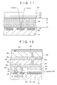
- Fig. 11 shows the fundamental configuration of a liquid crystal electro-optical device constituting a display apparatus which is represented by the preferred embodiment.
- This device serving as a reflex liquid crystal display device 23 comprises a silicon driving circuit substrate 31 composed of single crystal of silicon or the like and having a light reflective electrode 30 of a pixel structure, and a transparent substrate 33 of glass or the like having a transparent electrode 32 and positioned opposite to the substrate 31, wherein a vertically-aligned liquid crystal 36 is sealed between the two substrates (actually between liquid crystal orientation films 34 and 35).
- a reflective electrode substrate serving as the driving circuit substrate is such that a driving circuit comprising CMOS and n-channel MOS transistors Tr and capacitors C is formed on a single crystal silicon substrate 37, and a light reflective electrode 30 of a pixel structure is formed thereon with a metal film of aluminum, silver or the like.
- the light reflective electrode is composed of metal such as aluminum, it functions as both a light reflecting film and an electrode to apply a voltage to the liquid crystal.
- a light reflective layer with a multi-layer film such as a dielectric mirror may also be formed on the aluminum electrode.
- the transistor Tr comprises, for example, an n-type source region 38, a drain region 39, a gate insulating film 40 and a gate electrode 41, wherein electrodes 42 and 43 are led out from the active regions respectively.
- the electrode 43 is connected via an inter-layer insulating film 47 to a capacitor electrode 46 which is in contact with an insulating film (dielectric film) 45 on an n-type region 44 constituting a capacitor C.
- the electrode 43 is connected also to a wire 50 via inter-layer insulating films 48, 49 and further to the light reflective electrode 30.
- the layer thickness d (cell gap) of the vertically-aligned liquid crystal 36 is set to be equal to or less than 2 ⁇ m, and the refractive index anisotropy ⁇ n of the vertically-aligned liquid crystal 36 employed here is more than 0,1.
- Fig. 13 shows a fundamental layout of the display device and an equivalent circuit of its pixel portion.
- the silicon driving circuit substrate 31 comprises a pixel driving circuit formed in each pixel, and a logic driver circuit (data driver, scanning driver and so forth) incorporated in the periphery of a display area.
- the pixel driving circuit formed under each light reflective (pixel) electrode 30 consists of a switching transistor Tr and an auxiliary capacitance C for supplying a voltage to the vertically-aligned liquid crystal 36.
- the transistor Tr is required to withstand a predetermined voltage corresponding to the driving voltage for the vertically-aligned liquid crystal, and it is produced normally by a higher withstand voltage process as compared with the logic.
- the transistor size becomes greater with a rise of the withstand voltage, usually a transistor having a withstand voltage of 8 to 12 V or so is used in view of the production cost and the power consumption. Therefore, it is desired to design that the liquid crystal driving voltage is set within ⁇ 6 V. This requirement can be met according to the present invention.
- each molecule is so oriented that the major axis thereof is rendered substantially vertical to the substrate when no voltage is applied, and upon application of a voltage, the major axis is inclined to the in-plane direction to thereby change the transmissivity. If the inclinations of the liquid crystal molecules are not the same directionally when the liquid crystal is driven, there occurs some non-uniformity in brightness and darkness. In order to avoid such a disadvantage, it is necessary to vertically orient the liquid crystal by previously giving a slight pretilt angle in a fixed direction (generally in the diagonal direction of the device) as shown in Fig. 11.
- the pretilt angle is controlled generally within a range of 1° to 7°.
- Each of the liquid crystal orientation films 34 and 35 to be given such a pretilt angle is composed of a silicon oxide film represented by SiO 2 , such as an oblique evaporated film, or a polyimide film.
- the evaporation angle given at the time of oblique evaporation is in a range of 45° to 55°: meanwhile in the latter, the pretilt angle is controlled within a range of 1° to 7° by changing the rubbing condition.
- the thickness d of the vertically-aligned liquid crystal layer in the device structure of Fig. 11 is approximately 3 to 4 ⁇ m, and there is used a selected liquid crystal material where the refractive index anisotropy ⁇ n is less than 0,1 (typically 0,08 or so).
- the thickness d of the liquid crystal layer in the known device is reduced to less than 2,5 ⁇ m, the response speed is rendered higher but the driving voltage is raised as described above, so that the requirements for practical use fail to be satisfied.
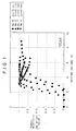
- Figs. 1 and 2 graphically show V-T curves obtained by changing the anisotropy ⁇ n of the liquid crystal under conditions that the thickness d of the liquid crystal layer is 2 ⁇ m and 1,5 ⁇ m, respectively. It is seen from these diagrams that, despite reduction of the thickness d of the liquid crystal layer to less than 2 ⁇ m in particular, the transmissivity is easily saturated at a low voltage of 4 to 6 V or less if the anisotropy ⁇ n is held over 0,1, whereby practical driving is achievable.
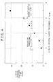
- Fig. 4 graphically shows the response speed (rise time + fall time) of the reflex liquid crystal display device according to the present invention.
- the fast response is kept under 8 msec even in a half tone.
- This device is capable of realizing a satisfactory image quality even in motion pictures of movies or television pictures where half-tone display is frequently employed with many moving images.
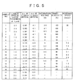
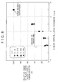
- Fig. 5 is a table showing the characteristics of the display device (samples Nos. 7 - 15) of the present invention and those of comparative examples (samples Nos. 1 - 6. 16 - 19).
- Fig. 6 graphically shows changes of a saturation voltage with ⁇ n in relation to the thickness d of a liquid crystal layer.
- suitable values adapted for practical use are as follows.
- the threshold voltage is considerably lowered, and saturation is attained at a driving voltage of approximately 2V.
- the response speed is in inverse proportion to the square of the driving voltage while being changed in conformity with the thickness d of the liquid crystal layer, so that such a low driving voltage extremely deteriorates the response speed.
- the black-and-white response speed of this device is 46 msec (approx. 50 msec), and in a half tone, the response speed is lowered to 100 msec or so due to a further drop of the driving voltage, hence causing manifest difficulty for practical use.
- it is necessary to reduce the value of ⁇ n under 0,1 in view of the response speed.
- the present invention has been accomplished by newly finding the requisite value of ⁇ n of the liquid crystal material so as to realize an improved reflex vertically-aligned liquid crystal device where the thickness d of its liquid crystal layer is less than 2 ⁇ m. Therefore, even if the thickness d of the liquid crystal layer is less than 2 ⁇ m, the saturation voltage can be lowered by selectively adjusting the refractive index anisotropy as ⁇ n ⁇ 0,1, hence enhancing the response speed as well.
- the vertically-aligned liquid crystal display device of the invention is more effective for an optical unit of a smaller F number as compared with any known device.
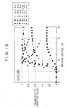
- each black level value (black-state transmissivity at zero voltage) in the vertically-aligned liquid crystal display device of the invention is graphically shown as a function of the thickness of the liquid crystal layer.
- the numerical values obtained with a layer thickness of 3,5 ⁇ m are expressed as 100% (where the abscissa represents the thickness of the liquid crystal layer).
- the liquid crystal molecules When the applied voltage is zero, the liquid crystal molecules are oriented to be substantially vertical to the substrate plane, so that in principle the incident light is reflected without any change of the polarized state and then is returned to the incidence side by means of a polarized beam splitter.
- the liquid crystal molecules are inclined at a pretilt angle and are therefore rendered slightly elliptical, and moreover the light separation characteristic of the polarized beam splitter is dependent on the incidence angle as mentioned, whereby the black-state transmissivity is raised to consequently deteriorate the contrast.
- the black-state transmissivity is lowered with a reduction of the thickness of the liquid crystal layer and, as shown in Fig. 8, the black level value obtained with a layer thickness of 2 ⁇ m becomes 20 - 30% as compared with the value in the known device, or 10 - 20% with a layer thickness of 1,5 ⁇ m, or 5 - 15% with a layer thickness of 1,0 ⁇ m. (But when the layer thickness is 2,5 ⁇ m, the black level value becomes high as 40 - 50%). Regarding the contrast which is expressed by the ratio of white and black levels, since the white level is kept substantially unchanged, the result shown in Fig. 8 indicates that the contrast attained in the device of the present invention becomes higher than five to ten times or more with a layer thickness of 1,5 ⁇ m for example.
- the transmissivity T of the liquid crystal in the device of the present invention is expressed by Eq. (4). T ⁇ sin 2 2 ⁇ d ⁇ ⁇ n eff ⁇ ⁇ / ⁇
- ⁇ denotes the wavelength of the light
- ⁇ n(eff) denotes the effective refractive index anisotropy corresponding to the inclination angle ⁇ from the perpendicular direction of liquid crystal molecules.
- This anisotropy is expressed by Eq. (5).
- ⁇ n eff n ⁇ ⁇ n ⁇ n ⁇ ⁇ 2 ⁇ cos 2 ⁇ + n ⁇ ⁇ 2 ⁇ sin 2 ⁇ - n ⁇
- the black level value i.e., the transmissivity in a black state
- the liquid crystal molecules are oriented with a pretilt angle of 1° to 7° as mentioned, whereby the value of ⁇ n(eff) is rendered finite to consequently give the black-state transmissivity.
- the black-state transmissivity is raised with an increase of the pretilt angle, it is preferred that the pretilt angle be controlled to less than 5°. Since 2d ⁇ n(eff) - ⁇ / ⁇ has a small value at the black level, Eq.
- T is theoretically considered to be proportional to the square of the thickness d of the liquid crystal layer.
- the thickness d of the liquid crystal layer in this device is so designed as to be less than 2 ⁇ m, and therefore the black level can be suppressed low essentially in comparison the known device where the layer thickness is 3 to 4 ⁇ m, hence realizing a high contrast.
- the black level in the device itself is held extremely low as explained, so that a sufficiently high contrast can be ensured even in the optical unit having a small F number.
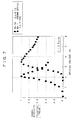
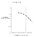
- Fig. 9 graphically shows changes caused in the black-state transmissivity by changing the F number of the projection lens 5 in Fig. 17 and that of the measuring optical unit corresponding to the illumination optical unit.
- the black level rises with a decrease of the F number, but in the device of the present invention, the black level is kept lower than in the known device at any F number, whereby a sufficiently high contrast can be realized even in the optical unit having a smaller F number under 3.
- a satisfactory high luminance is still attained with an F number of less than 3, as shown in Fig. 10. (However, the luminance is saturated when the F number is under 2). And the luminance is considerably lowered if the F number exceeds 3.
- the luminance is enhanced approximately 60% when the F number is changed from 3,85 to 2.
- a superior projection system which is capable of meeting the requirements for both a higher contrast and a higher luminance in comparison with any known system using the conventional device and optical unit, can be provided due to the display device of the present invention and also to a projection optical system and a projection display system each employing an optical unit of an F number under 3.
- Each conventional known device was produced as follows. First, a glass substrate with a transparent electrode and a driving circuit substrate of silicon with an aluminum electrode were washed and then were introduced into an evaporator, where a liquid crystal orientation film of SiO 2 was formed by oblique evaporation in an angular range of 45 to 55°. The thickness of the liquid crystal orientation film was set to 50 nm, and the pretilt angle of the liquid crystal was so controlled as to be approximately 2,5°.
- Fig. 15 graphically shows the liquid crystal driving characteristics of such devices. As shown in Figs. 15 and 16, the saturation driving voltage rises sharply over 6V when the thickness of the liquid crystal layer is less than 2,5 ⁇ m.
- a liquid crystal orientation film of SiO 2 was formed on each of a substrate with a transparent electrode and a driving circuit substrate of silicon with an aluminum electrode, and three kinds of vertically-aligned liquid crystal materials (made by Merck Ltd..) having a negative permittivity anisotropy ⁇ and a refractive index anisotropy ⁇ n of 0,103, 0,114 and 0,13 were injected between the two substrates to thereby produce nine kinds of reflex liquid crystal display devices (samples Nos. 7 - 15 in Fig. 5) where the liquid crystal layer thickness (cell gap) was 2 ⁇ m. 1,5 ⁇ m and 1 ⁇ m respectively.
- the pretilt angle of the liquid crystal was so controlled as to be approximately 2.5°.
- Figs. 1, 2 and 3 graphically show the driving characteristics obtained in three cases where the thickness of the liquid crystal layer is 2 ⁇ m, 1.5 ⁇ m and 1 ⁇ m respectively.
- Fig. 5 is a table showing the driving voltages of the individual devices at which the transmissivity is saturated substantially, and also the respective values of the transmissivity.
- the response speed changes substantially in proportion to the square of the thickness of the liquid crystal layer.
- the layer thickness d is less than 2 ⁇ m and ⁇ n is more than 0,1
- the driving voltage in the device (sample No. 16) was much lower.
- the response speed measured at room temperature in the same manner as in Embodiment 2 was 46 msec. Since the driving voltage in a half tone is low as 1V or so, the response speed was rendered lower, and in a gray-scale gradation of 25 %, the response speed was further lowered to the vicinity of 100 msec.
- the transmissivity (black level) at a zero applied voltage (black state) was measured in the reflex liquid crystal display device produced in Embodiment 1.
- devices having a layer thickness of 3,5 ⁇ m were produced with the aforementioned samples of ⁇ n, and also devices having a layer thickness of 2,5 ⁇ m were produced similarly, and the black-level transmissivity of each device was measured together with the samples (Nos. 7 - 15) of Embodiment 1.
- the respective black level values are graphically shown in Fig. 8 where the numerical values obtained in the devices with a layer thickness of 3,5 ⁇ m are indicated as 100% with the individual samples of ⁇ n.
- the black level is extremely lowered when the liquid crystal layer becomes thinner than 2 ⁇ m in any sample of ⁇ n.
- the indicated black level is lower by 10 to 20 % than the value obtained in any device with a layer thickness of 3,5 ⁇ m. That is, the contrast of the device becomes so high as 5 to 10 times.
- the measuring optical unit of Fig. 7 having an F number of 3,85 this trend remained substantially the same despite any change of the F number.
- Fig. 9 graphically shows the results of such comparison.
- the black level rises with a decrease of the F number.
- the black level is maintained lower than that in the known device despite any change of the F number.
- the white level transmissivity in each device was kept substantially unchanged at 0.6 or so. Therefore, the black level ratio directly gives the contrast ratio of the device.
- the lower limit of the F number may be set preferably to 1,5, further preferably to 2,0.
- a diagonally 0,7-inch silicon reflex type vertically-aligned liquid crystal display device was produced, and the luminance obtained by the use of a 120 W lamp as a light source was compared in a practical projection optical unit having an F number of 3,85, 3,5, 3, 2,5 and 2.
- the contrast attained was higher than the value in the known device, as mentioned. That is, a superior projection system was realized to meet the requirements for both a higher luminance and a higher contrast in comparison with those in the known device.
- the structure, material and so forth of the component parts of the reflex liquid crystal display device or those of an optical or projection system equipped with such display device are not limited merely to the aforementioned ones alone, and may be altered with a variety of modifications.
- the transmissivity of the liquid crystal is saturated with facility at a low voltage below 5 to 6 V despite a reduction of the thickness of the vertically-aligned liquid crystal layer to less than 2 ⁇ m, hence achieving satisfactory driving at a practically low voltage while attaining another advantage of remarkable improvement in the transmissivity itself. Therefore, it becomes possible to realize a superior reflex type vertically-aligned liquid crystal display device which indicates a sufficient transmissivity, an excellent low-voltage driving characteristic (low required withstand voltage) and fast response as well.
- the black level which is considered to be proportional to the square of the thickness of the liquid crystal layer, can be held low to thereby achieve a high contrast even when the F number of the optical unit is less than 3, and a high luminance is also achievable with a small F number. Consequently, it becomes possible to provide a superior system which is capable of satisfying the requirements for both a high contrast and a high luminance.
- a reflex liquid crystal display device may comprise a first substrate with a light transmissive electrode, a second substrate with a light reflective electrode, and a layer of vertically-aligned liquid crystal material interposed between said first and second substrates positioned opposite to each other in a state where said light transmissive electrode and said light reflective electrode are opposed mutually, wherein the thickness of said vertically-aligned liquid crystal layer is less than 2 ⁇ m, and the refractive index anisotropy ⁇ n of said liquid crystal material is more than 0,1.
- a liquid crystal orientation film may be formed on each of the mutually opposed faces of said light transmissive electrode being transparent and said light reflective electrode, and said light reflective electrode is connected to a single-crystal semiconductor driving circuit of silicon or the like formed on said second substrate, thereby constituting an active driving type reflex liquid crystal display device.
- Said single-crystal semiconductor driving circuit may comprise a driving transistor provided for each pixel on a silicon substrate serving as said second substrate, and said light reflective electrode is connected to the output side of said driving transistor.
- the pixel size may be less than 10 ⁇ m.
- a silicon oxide film may be formed as said liquid crystal orientation film.
- a display apparatus may be equipped with a reflex liquid crystal display device according to the above description.
- the display apparatus may comprise a light source, an optical unit for enabling incidence of the emitted light from the light source onto the reflex liquid crystal display device, said reflex liquid crystal display device, and an optical unit for introducing the reflected light from said reflex liquid crystal display device, wherein all of said components are disposed in an optical path of said apparatus.
- the light emitted from said light source may be incident upon said reflex liquid crystal display device via a polarizer/converter and a polarized beam splitter, and the reflected light from said reflex liquid crystal display device may be introduced via said polarized beam splitter again.
- Said reflex liquid crystal display device and said polarized beam splitter may be disposed for each of colors respectively, and the reflected light beams from the individual reflex liquid crystal display devices are synthesized.
- White light emitted from a white light source may be introduced to a dichroic color separation filter via said polarizer/converter, and the light beams separated therethrough may be further separated into light beams of individual colors, which are then incident upon said reflex liquid crystal display devices respectively via said polarized beam splitter, and the reflected light beams are synthesized by means of a prism.
- the reflex liquid crystal display device In a projection optical system the reflex liquid crystal display device according to the above description may be disposed in an optical path thereof.
- the projection optical system may comprise a light source, an optical unit for enabling incidence of the emitted light from the light source onto the reflex liquid crystal display device, said reflex liquid crystal display device, and an optical unit for introducing the reflected light from said reflex liquid crystal display device, wherein all of said components are disposed in an optical path of said system.
- the light emitted from said light source may be incident upon said reflex liquid crystal display device via a polarizer/converter and a polarized beam splitter, and the reflected light from said reflex liquid crystal display device may be introduced to a projection lens via said polarized beam splitter again.
- Said reflex liquid crystal display device and said polarized beam splitter may be disposed for each of colors respectively, and the reflected light beams from the individual reflex liquid crystal display devices may be synthesized and introduced to said projection lens.
- White light emitted from a white light source may be introduced to a dichroic color separation filter via said polarizer/converter, and the light beams separated therethrough may be further separated into light beams of individual colors, which are then incident upon said reflex liquid crystal display devices respectively via said polarized beam splitter, and the reflected light beams are synthesized by means of a prism.
- the reflex liquid crystal display device in a projection display system may be disposed in an optical path thereof.
- the projection display system may comprise a light source, an optical unit for enabling incidence of the emitted light from the light source onto the reflex liquid crystal display device, said reflex liquid crystal display device, and an optical unit for introducing the reflected light from said reflex liquid crystal display device, wherein all of said components are disposed in the optical path of said system.
- the light emitted from said light source may be incident upon said reflex liquid crystal display device via a polarizer/converter and a polarized beam splitter, and the reflected light from said reflex liquid crystal display device may be introduced to a projection lens via said polarized beam splitter again, and further to a screen.
- Said reflex liquid crystal display device and said polarized beam splitter may be disposed for each of colors respectively, and the reflected light beams from the individual reflex liquid crystal display devices may be synthesized and introduced to said projection lens.
- White light emitted from a white light source may be introduced to a dichroic color separation filter via said polarizer/converter, and the light beams separated therethrough may be further separated into light beams of individual colors, which are then incident upon said reflex liquid crystal display devices respectively via said polarized beam splitter, and the reflected light beams are synthesized by means of a prism.
- the projection optical system may comprise a light source, an optical unit for enabling incidence of the emitted light from the light source onto the reflex liquid crystal display device, said reflex liquid crystal display device, and an optical unit for introducing the reflected light from said reflex liquid crystal display device, wherein all of said components are disposed in the optical path of said system.
- the light emitted from said light source may be incident upon said reflex liquid crystal display device via a polarizer/converter and a polarized beam splitter, and the reflected light from said reflex liquid crystal display device may be introduced to a projection lens via said polarized beam splitter again.
- Said reflex liquid crystal display device and said polarized beam splitter may be disposed for each of colors respectively, and the reflected light beams from the individual reflex liquid crystal display devices may be synthesized and introduced to said projection lens.
- White light emitted from a white light source may be introduced to a dichroic color separation filter via said polarizer/converter, and the light beams separated therethrough may be further separated into light beams of individual colors, which are then incident upon said reflex liquid crystal display devices respectively via said polarized beam splitter, and the reflected light beams are synthesized by means of a prism.
- a reflex liquid crystal display device In a projection display system a reflex liquid crystal display device according to the above description, and an optical unit having an F number under 3, may be disposed in an optical path thereof.
- the projection display system may comprise a light source, an optical unit for enabling incidence of the emitted light from the light source onto the reflex liquid crystal display device, said reflex liquid crystal display device, and an optical unit for introducing the reflected light from said reflex liquid crystal display device, wherein all of said components are disposed in the optical path of said system.
- the light emitted from said light source may be incident upon said reflex liquid crystal display device via a polarizer/converter and a polarized beam splitter, and the reflected light from said reflex liquid crystal display device may be introduced to a projection lens via said polarized beam splitter again, and further to a screen.
- Said reflex liquid crystal display device and said polarized beam splitter may be disposed for each of colors respectively, and the reflected light beams from the individual reflex liquid crystal display devices may be synthesized and introduced to said projection lens.
- White light emitted from a white light source may be introduced to a dichroic color separation filter via said polarizer/converter, and the light beams separated therethrough may be further separated into light beams of individual colors, which are then incident upon said reflex liquid crystal display devices respectively via said polarized beam splitter, and the reflected light beams are synthesized by means of a prism.
- a reflex liquid crystal display device and an optical unit having an F number under 3 are disposed in an optical path thereof, said reflex liquid crystal display device comprising a first substrate with a light transmissive electrode, a second substrate with a light reflective electrode; and a layer of vertically-aligned liquid crystal material interposed between said first and second substrates positioned opposite to each other in a state where said light transmissive electrode and said light reflective electrode have mutually opposed faces, wherein the thickness of said vertically-aligned liquid crystal layer is 2 ⁇ m or less, wherein the refractive index anisotropy ⁇ n of said liquid crystal material is more than 0,1, and wherein said vertically aligned liquid crystal layer includes a plurality of liquid crystal molecules each having a pre-tilt angle controlled within a range of 1° to 7°.
- Said Projection optical system may comprise a light source, an optical unit for enabling incidence of the emitted light from the light source onto the reflex liquid crystal display device, said reflex liquid crystal display device, and an optical unit for introducing the reflected light from said reflex liquid crystal display device, wherein all of said components are disposed in the optical path of said system.
- the light emitted from said light source may be incident upon said reflex liquid crystal display device via a polarizer/converter and a polarized beam splitter.
- the reflected light from said reflex liquid crystal display device may be introduced to a projection lens via said polarized beam splitter again.
- Said reflex liquid crystal display device and said polarized beam splitter may be disposed for each of colors respectively
- the reflected light beams from the individual reflex liquid crystal display devices may be synthesized and introduced to said projection lens.
- White light emitted from a white light source may be introduced to a dichroic color separation filter via said polarizer/converter.
- the light beams separated there through may be further separated into light means of individual colors, which may then be incident upon said reflex liquid crystal display devices respectively via said polarized beam splitter.
- the reflected light beams may be synthesized by means of a prism.
- a projection optical system wherein a reflex liquid crystal display device and an optical unit having an F number under 3 are disposed in an optical path thereof, said reflex liquid crystal display device comprising a first substrate with a light transmissive electrode, a second substrate with a light reflective electrode, and a layer of vertically-aligned liquid crystal material interposed between said first and second substrates positioned opposite to each other in a state where said light transmissive electrode and said light reflective electrode have mutually opposed faces, wherein the thickness of said vertically-aligned liquid crystal layer is 2 ⁇ m or less, wherein the refractive index anisotropy ⁇ n of said liquid crystal material is more than 0,1, and wherein said vertically aligned liquid crystal layer includes a plurality of liquid crystal molecules each having a pre-tilt angle controlled within a range of 1° ° to 7°.
- the projection display system may comprising a light source, an optical unit for enabling incidence of the emitted light from the light source onto the reflex liquid crystal display device, said reflex liquid crystal display device, and an optical unit for introducing the reflected light from said reflex liquid crystal display device, wherein all of said components are disposed in the optical path of said system.
- the light emitted from said light source may be incident upon said reflex liquid crystal display device via a polarizer/converter and a polarized beam splitter.
- the reflected light from said reflex liquid crystal display device may be introduced to a projection lens via said polarized beam splitter again, and further to a screen.
- aid reflex liquid crystal display device and said polarized beam splitter may be disposed for each of colors respectively.
- the reflected light beams from the individual reflex liquid crystal display devices may be synthesized and introduced to said projection lens.
- White light emitted from a white light source is introduced to a dichroic color separation filter via said polarizer/converter.
- the light beams separated there through may be further separated into light means of individual colors, which are then incident upon said reflex liquid crystal display devices respectively via said polarized beam splitter.
- the reflected light beams may be synthesized by means of a prism.
- a transparent alignment film may be formed on each of the mutually opposed faces of said light transmissive electrode and said light reflective electrode.
- Said light reflective electrode may be connected to a single-crystal semiconductor driving circuit of silicon or the like formed on said second substrate.
- an active driving type reflex liquid crystal display device may be constituted.
- Said sirigle-crystal semiconductor driving circuit may comprise a driving transistor provided for each pixel on a silicon substrate serving as said second substrate.
- Said light reflective electrode may be connected to the output side of said driving transistor.
- a voltage for saturating a light output with respect to a light input to said layer may be within a range of 6 Volt.
- Said voltage may be under a withstand voltage of the driving transistor.
- An oblique evaporated silicon oxide film may be formed as said alignment film.
- a pixel may be comprised that incorporates said light reflective electrode.
- the pixel may have a size of less than 10 ⁇ m.
- Each of the plurality of liquid crystal molecules may have a pre-tilt angle controlled within a range of 1° to 5°.
- the refractive index anisotropy ⁇ n of the liquid crystal material is more than 0,11.
- a superior reflex type vertically-aligned liquid crystal display device wherein the refractive index anisotropy ⁇ n of its liquid crystal material is controlled to be more than 0,1, and the transmissivity of the liquid crystal is saturated with facility at a low voltage below 5 to 6 V despite a reduction of the thickness of the vertically-aligned liquid crystal layer to less than 2 ⁇ m, hence achieving satisfactory driving at a practically low voltage while attaining another advantage of remarkable improvement in the transmissivity itself. Therefore, the display device indicates a sufficient transmissivity, an excellent low-voltage driving characteristic and a fast response. Further improvements are realizable in a display apparatus, a projection optical system and a projection display system by the use of such display device.
Landscapes
- Physics & Mathematics (AREA)
- Nonlinear Science (AREA)
- Engineering & Computer Science (AREA)
- General Physics & Mathematics (AREA)
- Crystallography & Structural Chemistry (AREA)
- Chemical & Material Sciences (AREA)
- Optics & Photonics (AREA)
- Multimedia (AREA)
- Signal Processing (AREA)
- Mathematical Physics (AREA)
- Microelectronics & Electronic Packaging (AREA)
- Spectroscopy & Molecular Physics (AREA)
- Liquid Crystal (AREA)
- Projection Apparatus (AREA)
Applications Claiming Priority (2)
| Application Number | Priority Date | Filing Date | Title |
|---|---|---|---|
| JP2001192203 | 2001-06-26 | ||
| EP02738809A EP1400837A4 (de) | 2001-06-26 | 2002-06-26 | Flüssigkristallanzeigeelement des reflexionstyps, anzeigeeinheit, optisches prädiktionssystem und projektionsanzeigesystem |
Related Parent Applications (1)
| Application Number | Title | Priority Date | Filing Date |
|---|---|---|---|
| EP02738809A Division EP1400837A4 (de) | 2001-06-26 | 2002-06-26 | Flüssigkristallanzeigeelement des reflexionstyps, anzeigeeinheit, optisches prädiktionssystem und projektionsanzeigesystem |
Publications (2)
| Publication Number | Publication Date |
|---|---|
| EP1783541A2 true EP1783541A2 (de) | 2007-05-09 |
| EP1783541A3 EP1783541A3 (de) | 2007-05-23 |
Family
ID=19030691
Family Applications (2)
| Application Number | Title | Priority Date | Filing Date |
|---|---|---|---|
| EP02738809A Ceased EP1400837A4 (de) | 2001-06-26 | 2002-06-26 | Flüssigkristallanzeigeelement des reflexionstyps, anzeigeeinheit, optisches prädiktionssystem und projektionsanzeigesystem |
| EP07002548A Ceased EP1783541A3 (de) | 2001-06-26 | 2002-06-26 | Optisches Projektionssystem |
Family Applications Before (1)
| Application Number | Title | Priority Date | Filing Date |
|---|---|---|---|
| EP02738809A Ceased EP1400837A4 (de) | 2001-06-26 | 2002-06-26 | Flüssigkristallanzeigeelement des reflexionstyps, anzeigeeinheit, optisches prädiktionssystem und projektionsanzeigesystem |
Country Status (5)
| Country | Link |
|---|---|
| US (2) | US7330230B2 (de) |
| EP (2) | EP1400837A4 (de) |
| KR (1) | KR100915311B1 (de) |
| CN (2) | CN1267777C (de) |
| WO (1) | WO2003001285A1 (de) |
Families Citing this family (20)
| Publication number | Priority date | Publication date | Assignee | Title |
|---|---|---|---|---|
| KR100754165B1 (ko) * | 2003-11-06 | 2007-09-03 | 삼성전자주식회사 | 반사형 액정표시소자 및 이를 이용한 프로젝터 |
| US8462299B2 (en) * | 2004-03-05 | 2013-06-11 | Sony Corporation | Reflection type liquid crystal display device, display apparatus, and projection system |
| US8885139B2 (en) * | 2005-01-21 | 2014-11-11 | Johnson & Johnson Vision Care | Adaptive electro-active lens with variable focal length |
| JP2006337791A (ja) * | 2005-06-03 | 2006-12-14 | Hitachi Ltd | 投射型映像表示装置、それに用いる光学ユニット及び偏光分離用部材 |
| DE102005050322B4 (de) * | 2005-10-20 | 2009-11-26 | Cinetron Technology Inc. | Modulares Lichtstrahl-Rekombinierungssystem und zugehöriges Lichtstrahl-Rekombinierungsverfahren |
| MX2008015907A (es) * | 2006-06-12 | 2009-01-14 | Johnson & Johnson Vision Care | Metodo para reducir consumo de energia con lentes electro-opticos. |
| JP2010503026A (ja) * | 2006-09-01 | 2010-01-28 | ジョンソン・アンド・ジョンソン・ビジョン・ケア・インコーポレイテッド | 抵抗性電極を使用する電気光学レンズ |
| KR20110078788A (ko) * | 2009-12-31 | 2011-07-07 | 엘지디스플레이 주식회사 | 액정 전계 렌즈 및 이를 이용한 입체 표시 장치 |
| JP2011227404A (ja) * | 2010-04-22 | 2011-11-10 | Sony Corp | 光学装置及び投影装置 |
| CN102650790B (zh) * | 2011-07-25 | 2015-01-07 | 京东方科技集团股份有限公司 | 应用液晶透镜结构的液晶显示器 |
| TWI452396B (zh) * | 2011-10-06 | 2014-09-11 | Univ Nat Chiao Tung | 可電壓控制之光學元件及其製備方法 |
| DE102012205373A1 (de) * | 2012-04-02 | 2013-10-02 | Kyocera Display Europe Gmbh | Senkrecht orientierendes Flüssigkristalldisplay mit multiplen "Pretilt"-Winkeln und Herstellungsverfahren hierfür |
| EP2873999A4 (de) * | 2012-06-29 | 2016-06-08 | Shanghai Tianma Micro Elect Co | Kapazitiver berührungsbildschirm mit flüssigkristallanzeige |
| TWI510506B (zh) * | 2012-12-14 | 2015-12-01 | Lg化學股份有限公司 | 聚合性組成物 |
| KR20150049630A (ko) | 2013-10-30 | 2015-05-08 | 삼성디스플레이 주식회사 | 표시 장치 |
| KR102274545B1 (ko) * | 2014-12-01 | 2021-07-06 | 삼성전자주식회사 | 광학 필름용 조성물, 필름 및 표시 장치 |
| CN205942207U (zh) * | 2016-05-17 | 2017-02-08 | 京东方科技集团股份有限公司 | 一种显示面板及显示装置 |
| US11361215B2 (en) | 2017-11-29 | 2022-06-14 | Anaflash Inc. | Neural network circuits having non-volatile synapse arrays |
| JP2019124775A (ja) * | 2018-01-15 | 2019-07-25 | セイコーエプソン株式会社 | 液晶装置および電子機器 |
| JP2023147682A (ja) * | 2022-03-30 | 2023-10-13 | セイコーエプソン株式会社 | 表示装置及び複合表示装置 |
Family Cites Families (45)
| Publication number | Priority date | Publication date | Assignee | Title |
|---|---|---|---|---|
| NL8701347A (nl) * | 1987-06-10 | 1989-01-02 | Philips Nv | Vloeibaar kristal weergeefinrichting en werkwijze ter vervaardiging van een dergelijke weergeefinrichting. |
| US5329387A (en) * | 1990-11-27 | 1994-07-12 | Casio Computer Co., Ltd. | Liquid crystal display device with display and compensation cells separated by distance larger than depth of focus of optical enlarger |
| JP3132193B2 (ja) * | 1991-11-08 | 2001-02-05 | 日本ビクター株式会社 | 液晶表示デバイス及び液晶表示デバイスの製造方法 |
| US5309264A (en) * | 1992-04-30 | 1994-05-03 | International Business Machines Corporation | Liquid crystal displays having multi-domain cells |
| JP3313142B2 (ja) | 1992-07-03 | 2002-08-12 | 松下電器産業株式会社 | 液晶パネルおよびそれを用いた投写型表示装置 |
| US5532854A (en) * | 1994-01-25 | 1996-07-02 | Fergason; James L. | Folded variable birefringerence zeroth order hybrid aligned liquid crystal apparatus |
| TW294714B (de) * | 1995-03-02 | 1997-01-01 | Merck Patent Gmbh | |
| JP3143591B2 (ja) | 1995-09-14 | 2001-03-07 | キヤノン株式会社 | 表示装置 |
| WO1997045768A1 (en) | 1996-05-29 | 1997-12-04 | Seiko Epson Corporation | Projection display |
| US6155685A (en) * | 1996-10-31 | 2000-12-05 | Minolta Co., Ltd. | Projector |
| DE29705133U1 (de) | 1997-03-20 | 1997-07-24 | Trw Repa Gmbh | Gassack für ein Fahrzeuginsassen-Schutzsystem |
| US5919606A (en) * | 1997-05-09 | 1999-07-06 | University Technology Corporation | Liquid crystal cell and method for assembly thereof |
| JPH1164852A (ja) * | 1997-08-21 | 1999-03-05 | Hitachi Ltd | 投射型液晶表示装置 |
| JPH1184419A (ja) | 1997-09-09 | 1999-03-26 | Hitachi Ltd | 液晶ライトバルブおよび投射型表示装置 |
| JPH11153814A (ja) | 1997-09-17 | 1999-06-08 | Matsushita Electric Ind Co Ltd | 液晶表示素子 |
| JPH11149096A (ja) * | 1997-11-18 | 1999-06-02 | Sanyo Electric Co Ltd | 反射型液晶表示装置 |
| JP3501963B2 (ja) | 1997-12-22 | 2004-03-02 | シャープ株式会社 | 投影型画像表示装置 |
| JP3296771B2 (ja) | 1998-01-26 | 2002-07-02 | 株式会社日立製作所 | 液晶表示装置およびその駆動方法、および液晶プロジェクタ |
| JP4073533B2 (ja) | 1998-02-09 | 2008-04-09 | 株式会社半導体エネルギー研究所 | 情報処理装置 |
| JP3490886B2 (ja) | 1998-03-03 | 2004-01-26 | シャープ株式会社 | 投影型画像表示装置 |
| JPH11259018A (ja) * | 1998-03-10 | 1999-09-24 | Sony Corp | 拡散反射板の製造方法及び反射型表示装置 |
| US6273567B1 (en) * | 1998-09-14 | 2001-08-14 | Arlie R. Conner | Compact multi-path LCD projector |
| US6082861A (en) * | 1998-09-16 | 2000-07-04 | International Business Machines Corporation | Optical system and method for high contrast projection display |
| JP2000171770A (ja) | 1998-09-30 | 2000-06-23 | Sony Corp | 投射型表示装置 |
| US6300929B1 (en) * | 1998-12-28 | 2001-10-09 | Kabushiki Kaisha Toshiba | Flat panel display device |
| JP3887980B2 (ja) | 1999-01-22 | 2007-02-28 | セイコーエプソン株式会社 | 液晶装置及び電子機器 |
| JP2000214421A (ja) | 1999-01-22 | 2000-08-04 | Seiko Epson Corp | 液晶装置及び電子機器 |
| US6067142A (en) * | 1999-01-27 | 2000-05-23 | International Business Machines Corporation | Vertically aligned pi-cell LCD having on-state with mid-plane molecules perpendicular to the substrates |
| GB9902402D0 (en) | 1999-02-03 | 1999-03-24 | Rolic Ag | Method of imparting preferred alignment, and liquid crystal device elements incorporating a preferred alignment |
| US6498635B1 (en) | 1999-03-05 | 2002-12-24 | Chartered Semiconductor Manufacturing Ltd. | Method of forming insulating material alignment posts associated with active device structures |
| JP2000281664A (ja) | 1999-03-30 | 2000-10-10 | Otsuka Pharmaceut Co Ltd | チアゾール誘導体 |
| JP2000292815A (ja) * | 1999-04-12 | 2000-10-20 | Stanley Electric Co Ltd | 垂直配向型ecbモード液晶表示素子 |
| JP3554520B2 (ja) | 1999-07-08 | 2004-08-18 | シャープ株式会社 | 画像表示装置 |
| KR100294822B1 (ko) * | 1999-06-05 | 2001-07-12 | 구본준, 론 위라하디락사 | 반사형 액정표시소자. |
| JP4085526B2 (ja) | 1999-07-16 | 2008-05-14 | 松下電器産業株式会社 | 反射型ライトバルブを用いた投写型画像表示装置 |
| US6234634B1 (en) * | 1999-07-28 | 2001-05-22 | Moxtek | Image projection system with a polarizing beam splitter |
| JP2001117090A (ja) | 1999-10-20 | 2001-04-27 | Seiko Epson Corp | 反射型液晶装置及び反射型プロジェクタ |
| JP2001134652A (ja) | 1999-11-05 | 2001-05-18 | Aplix Corp | 在庫確認・予約システム |
| US6724449B1 (en) * | 2000-03-27 | 2004-04-20 | International Business Machines Corporation | Vertical aligned liquid crystal display and method using dry deposited alignment layer films |
| JP2001281664A (ja) * | 2000-03-30 | 2001-10-10 | Fujitsu Ltd | 液晶表示装置 |
| JP2001343652A (ja) * | 2000-05-30 | 2001-12-14 | Sharp Corp | 液晶表示素子 |
| KR100883004B1 (ko) * | 2000-11-23 | 2009-02-12 | 메르크 파텐트 게엠베하 | 호메오트로픽 얼라인먼트 층 |
| US20030058385A1 (en) | 2001-05-24 | 2003-03-27 | Mcknight Douglas J. | Liquid crystal display device |
| JP3758654B2 (ja) | 2001-06-26 | 2006-03-22 | ソニー株式会社 | プロジェクション光学システム及びプロジェクションディスプレイシステム |
| JP3758612B2 (ja) | 2001-06-26 | 2006-03-22 | ソニー株式会社 | 反射型液晶表示素子、表示装置、プロジェクション光学システム、及びプロジェクションディスプレイシステム |
-
2002
- 2002-06-26 CN CNB028028228A patent/CN1267777C/zh not_active Expired - Fee Related
- 2002-06-26 US US10/362,646 patent/US7330230B2/en not_active Expired - Lifetime
- 2002-06-26 EP EP02738809A patent/EP1400837A4/de not_active Ceased
- 2002-06-26 CN CNA2006100878774A patent/CN1862326A/zh active Pending
- 2002-06-26 EP EP07002548A patent/EP1783541A3/de not_active Ceased
- 2002-06-26 KR KR1020037002815A patent/KR100915311B1/ko not_active Expired - Fee Related
- 2002-06-26 WO PCT/JP2002/006443 patent/WO2003001285A1/ja not_active Ceased
-
2007
- 2007-12-14 US US11/957,136 patent/US7903212B2/en not_active Expired - Fee Related
Also Published As
| Publication number | Publication date |
|---|---|
| CN1267777C (zh) | 2006-08-02 |
| CN1473280A (zh) | 2004-02-04 |
| US7903212B2 (en) | 2011-03-08 |
| EP1783541A3 (de) | 2007-05-23 |
| US20040105038A1 (en) | 2004-06-03 |
| WO2003001285A1 (en) | 2003-01-03 |
| CN1862326A (zh) | 2006-11-15 |
| US7330230B2 (en) | 2008-02-12 |
| KR100915311B1 (ko) | 2009-09-03 |
| EP1400837A1 (de) | 2004-03-24 |
| US20080259258A1 (en) | 2008-10-23 |
| KR20030027090A (ko) | 2003-04-03 |
| EP1400837A4 (de) | 2005-05-18 |
Similar Documents
| Publication | Publication Date | Title |
|---|---|---|
| US7903212B2 (en) | Reflex liquid crystal display device, display apparatus, projection optical system, and projection display system | |
| US7227604B2 (en) | Reflective liquid crystal display device having first and second obliquely evaporated alignment films, for preventing burn-in | |
| EP0992838B1 (de) | Flüssigkristall-Anzeigevorrichtung | |
| JP2005156717A (ja) | 液晶表示素子及び液晶表示装置 | |
| CN1333299C (zh) | 反射型液晶显示装置、制造其的方法及液晶显示单元 | |
| US7362388B2 (en) | Liquid crystal display device, and optical block | |
| KR100447375B1 (ko) | 액정 장치 | |
| JP3758612B2 (ja) | 反射型液晶表示素子、表示装置、プロジェクション光学システム、及びプロジェクションディスプレイシステム | |
| US7106401B2 (en) | Reflex liquid crystal display device, display apparatus, projection optical system, and projection display system | |
| JP4029786B2 (ja) | 液晶表示素子及び液晶表示装置 | |
| KR101096410B1 (ko) | 반사형 액정 표시 소자, 표시 장치 및 프로젝션 시스템 | |
| JPH021816A (ja) | 投影型表示装置 | |
| JP3758654B2 (ja) | プロジェクション光学システム及びプロジェクションディスプレイシステム | |
| KR100804688B1 (ko) | 반사형 액정 디스플레이 및 이를 구비하는 프로젝션 시스템 | |
| US20050157227A1 (en) | Reflection type liquid crystal display element and liquid crystal display unit | |
| JP4143922B2 (ja) | プロジェクションディスプレイシステム | |
| JPH10221673A (ja) | 投射型カラー画像表示装置 | |
| JP2001133747A (ja) | 液晶装置とこれを用いた液晶表示装置 | |
| JPH05323311A (ja) | 液晶表示装置およびそれを用いた液晶投写型テレビ | |
| JP4862460B2 (ja) | 反射型液晶表示素子及びその製造方法並びに液晶表示装置 | |
| JP2002287152A (ja) | 液晶装置および投射型表示装置 | |
| JP2005024922A (ja) | 反射型液晶表示素子及び液晶表示装置 | |
| JP2004053671A (ja) | 反射型液晶素子を用いた投影装置 | |
| JPH11258568A (ja) | 表示装置 |
Legal Events
| Date | Code | Title | Description |
|---|---|---|---|
| PUAI | Public reference made under article 153(3) epc to a published international application that has entered the european phase |
Free format text: ORIGINAL CODE: 0009012 |
|
| PUAL | Search report despatched |
Free format text: ORIGINAL CODE: 0009013 |
|
| AC | Divisional application: reference to earlier application |
Ref document number: 1400837 Country of ref document: EP Kind code of ref document: P |
|
| AK | Designated contracting states |
Kind code of ref document: A2 Designated state(s): DE FR GB |
|
| AK | Designated contracting states |
Kind code of ref document: A3 Designated state(s): DE FR GB |
|
| 17P | Request for examination filed |
Effective date: 20071107 |
|
| 17Q | First examination report despatched |
Effective date: 20071213 |
|
| AKX | Designation fees paid |
Designated state(s): DE FR GB |
|
| STAA | Information on the status of an ep patent application or granted ep patent |
Free format text: STATUS: THE APPLICATION HAS BEEN REFUSED |
|
| 18R | Application refused |
Effective date: 20091201 |