EP1786023B1 - Simox substrate manufacturing method - Google Patents
Simox substrate manufacturing method Download PDFInfo
- Publication number
- EP1786023B1 EP1786023B1 EP05762053A EP05762053A EP1786023B1 EP 1786023 B1 EP1786023 B1 EP 1786023B1 EP 05762053 A EP05762053 A EP 05762053A EP 05762053 A EP05762053 A EP 05762053A EP 1786023 B1 EP1786023 B1 EP 1786023B1
- Authority
- EP
- European Patent Office
- Prior art keywords
- oxygen
- atmosphere
- gas
- silicon substrate
- substrate
- Prior art date
- Legal status (The legal status is an assumption and is not a legal conclusion. Google has not performed a legal analysis and makes no representation as to the accuracy of the status listed.)
- Expired - Fee Related
Links
Images
Classifications
-
- H—ELECTRICITY
- H10—SEMICONDUCTOR DEVICES; ELECTRIC SOLID-STATE DEVICES NOT OTHERWISE PROVIDED FOR
- H10P—GENERIC PROCESSES OR APPARATUS FOR THE MANUFACTURE OR TREATMENT OF DEVICES COVERED BY CLASS H10
- H10P95/00—Generic processes or apparatus for manufacture or treatments not covered by the other groups of this subclass
- H10P95/90—Thermal treatments, e.g. annealing or sintering
-
- H—ELECTRICITY
- H10—SEMICONDUCTOR DEVICES; ELECTRIC SOLID-STATE DEVICES NOT OTHERWISE PROVIDED FOR
- H10P—GENERIC PROCESSES OR APPARATUS FOR THE MANUFACTURE OR TREATMENT OF DEVICES COVERED BY CLASS H10
- H10P30/00—Ion implantation into wafers, substrates or parts of devices
- H10P30/20—Ion implantation into wafers, substrates or parts of devices into semiconductor materials, e.g. for doping
- H10P30/208—Ion implantation into wafers, substrates or parts of devices into semiconductor materials, e.g. for doping of electrically inactive species
- H10P30/209—Ion implantation into wafers, substrates or parts of devices into semiconductor materials, e.g. for doping of electrically inactive species in silicon to make buried insulating layers
-
- H—ELECTRICITY
- H10—SEMICONDUCTOR DEVICES; ELECTRIC SOLID-STATE DEVICES NOT OTHERWISE PROVIDED FOR
- H10P—GENERIC PROCESSES OR APPARATUS FOR THE MANUFACTURE OR TREATMENT OF DEVICES COVERED BY CLASS H10
- H10P14/00—Formation of materials, e.g. in the shape of layers or pillars
- H10P14/20—Formation of materials, e.g. in the shape of layers or pillars of semiconductor materials
-
- H—ELECTRICITY
- H10—SEMICONDUCTOR DEVICES; ELECTRIC SOLID-STATE DEVICES NOT OTHERWISE PROVIDED FOR
- H10P—GENERIC PROCESSES OR APPARATUS FOR THE MANUFACTURE OR TREATMENT OF DEVICES COVERED BY CLASS H10
- H10P14/00—Formation of materials, e.g. in the shape of layers or pillars
- H10P14/60—Formation of materials, e.g. in the shape of layers or pillars of insulating materials
- H10P14/63—Formation of materials, e.g. in the shape of layers or pillars of insulating materials characterised by the formation processes
- H10P14/6302—Non-deposition formation processes
- H10P14/6304—Formation by oxidation, e.g. oxidation of the substrate
- H10P14/6306—Formation by oxidation, e.g. oxidation of the substrate of the semiconductor materials
- H10P14/6308—Formation by oxidation, e.g. oxidation of the substrate of the semiconductor materials of Group IV semiconductors
- H10P14/6309—Formation by oxidation, e.g. oxidation of the substrate of the semiconductor materials of Group IV semiconductors of silicon in uncombined form, i.e. pure silicon
-
- H—ELECTRICITY
- H10—SEMICONDUCTOR DEVICES; ELECTRIC SOLID-STATE DEVICES NOT OTHERWISE PROVIDED FOR
- H10P—GENERIC PROCESSES OR APPARATUS FOR THE MANUFACTURE OR TREATMENT OF DEVICES COVERED BY CLASS H10
- H10P14/00—Formation of materials, e.g. in the shape of layers or pillars
- H10P14/60—Formation of materials, e.g. in the shape of layers or pillars of insulating materials
- H10P14/63—Formation of materials, e.g. in the shape of layers or pillars of insulating materials characterised by the formation processes
- H10P14/6302—Non-deposition formation processes
- H10P14/6322—Formation by thermal treatments
-
- H—ELECTRICITY
- H10—SEMICONDUCTOR DEVICES; ELECTRIC SOLID-STATE DEVICES NOT OTHERWISE PROVIDED FOR
- H10P—GENERIC PROCESSES OR APPARATUS FOR THE MANUFACTURE OR TREATMENT OF DEVICES COVERED BY CLASS H10
- H10P14/00—Formation of materials, e.g. in the shape of layers or pillars
- H10P14/60—Formation of materials, e.g. in the shape of layers or pillars of insulating materials
- H10P14/65—Formation of materials, e.g. in the shape of layers or pillars of insulating materials characterised by treatments performed before or after the formation of the materials
- H10P14/6502—Formation of materials, e.g. in the shape of layers or pillars of insulating materials characterised by treatments performed before or after the formation of the materials of treatments performed before formation of the materials
-
- H—ELECTRICITY
- H10—SEMICONDUCTOR DEVICES; ELECTRIC SOLID-STATE DEVICES NOT OTHERWISE PROVIDED FOR
- H10P—GENERIC PROCESSES OR APPARATUS FOR THE MANUFACTURE OR TREATMENT OF DEVICES COVERED BY CLASS H10
- H10P30/00—Ion implantation into wafers, substrates or parts of devices
- H10P30/20—Ion implantation into wafers, substrates or parts of devices into semiconductor materials, e.g. for doping
-
- H—ELECTRICITY
- H10—SEMICONDUCTOR DEVICES; ELECTRIC SOLID-STATE DEVICES NOT OTHERWISE PROVIDED FOR
- H10P—GENERIC PROCESSES OR APPARATUS FOR THE MANUFACTURE OR TREATMENT OF DEVICES COVERED BY CLASS H10
- H10P90/00—Preparation of wafers not covered by a single main group of this subclass, e.g. wafer reinforcement
- H10P90/19—Preparing inhomogeneous wafers
- H10P90/1904—Preparing vertically inhomogeneous wafers
- H10P90/1906—Preparing SOI wafers
- H10P90/1908—Preparing SOI wafers using silicon implanted buried insulating layers, e.g. oxide layers [SIMOX]
-
- H—ELECTRICITY
- H10—SEMICONDUCTOR DEVICES; ELECTRIC SOLID-STATE DEVICES NOT OTHERWISE PROVIDED FOR
- H10P—GENERIC PROCESSES OR APPARATUS FOR THE MANUFACTURE OR TREATMENT OF DEVICES COVERED BY CLASS H10
- H10P95/00—Generic processes or apparatus for manufacture or treatments not covered by the other groups of this subclass
-
- H—ELECTRICITY
- H10—SEMICONDUCTOR DEVICES; ELECTRIC SOLID-STATE DEVICES NOT OTHERWISE PROVIDED FOR
- H10W—GENERIC PACKAGES, INTERCONNECTIONS, CONNECTORS OR OTHER CONSTRUCTIONAL DETAILS OF DEVICES COVERED BY CLASS H10
- H10W10/00—Isolation regions in semiconductor bodies between components of integrated devices
- H10W10/10—Isolation regions comprising dielectric materials
- H10W10/181—Semiconductor-on-insulator [SOI] isolation regions, e.g. buried oxide regions of SOI wafers
Definitions
- the present invention relates to a manufacturing method for a SIMOX substrate for obtaining a SIMOX substrate by subjecting an oxygen-ion-implanted silicon substrate to heat treatment.
- SIMOX substrates are SOI substrates where oxygen ions are implanted into a single-crystal silicon substrate and then a high-temperature heat treatment is carried out in an oxidizing atmosphere to cause chemical reactions between the implanted oxygen ions and silicon atoms so that a buried oxide film is formed. Because devices formed on these SOI layers achieve high radioresistance, latch-up resistance, control of a short channel effect, and low-power-consumption operation, SOI substrates are expected as next-generation high-performance semiconductor substrates.
- crystal defects such as COPs (Crystal Originated Particles)
- COPs Crystal Originated Particles
- device manufacturers provide an improvement in yield due to poor insulation of a gate oxide film by using substrates with low crystal defect density, such as silicon epitaxial growth substrates or substrates with significantly reduced crystal defects that are grown at a low pull rate.
- any COPs or void defects existing on or near the substrate surface bring about, for example, a pinhole defect on a SOI layer surface of the finished product, thus degrading device characteristics.
- a manufacturing method for a SIMOX substrate is proposed which is free of pinhole defects on this SOI layer surface by using a silicon single crystal which includes 1 ⁇ 10 14 atoms/cm 3 to 1 ⁇ 10 17 atoms/cm 3 of nitrogen (refer to, for example, Japanese Unexamined Patent Application, First Publication No. H10-64837 ).
- Document JP-11040521 (12-02-1999) discloses a method to reduce transition density present at the surface of a SIMOX substrate, by performing different annealing process steps at different temperature in a reducing atmosphere.
- This invention provides a manufacturing method for a SIMOX substrate in which relatively small defects on a SOI layer surface can be eliminated.
- a manufacturing method according to this invention is an improved version of the method for manufacturing a SIMOX substrate for obtaining a SIMOX substrate by subjecting an oxygen-ion-implanted silicon substrate to heat treatment at 1300 to 1350°C in an atmosphere of a gas mixture of argon and oxygen.
- This method includes performing a pre-heat-treatment to the silicon substrate for five minutes to four hours within the temperature range of 1000°C to 1280°C in an atmosphere of inert gas, reducing gas, or a gas mixture of inert gas and reducing gas, after the oxygen ions are implanted and before the heat treatment is performed.
- an inner-wall oxide film of crystal defects resulting from heat treatment in an atmosphere of non-oxidizing gas is dissolved by subjecting the silicon substrate to pre-heat-treatment after oxygen ions have been implanted and before heat treatment is carried out, and thereafter grown-in defects adjacent to the surface are reduced and eliminated by drawing upon a gap-filling effect by diffusion of interstitial silicon atoms in void defects where the inner-wall oxide film has been removed. In this manner, defects of smaller than 0.3 ⁇ m in size can also be eliminated.
- the above-described silicon substrate into which oxygen ions are implanted may have crystal defect densities of void defects or COPs greater than or equal to 1 ⁇ 10 5 cm -3 and a maximum frequency less than or equal to 0.12 ⁇ m in the size distribution of crystal defects.
- the manufacturing method for a SIMOX substrate includes: decreasing the temperature of the silicon substrate to 600°C to 1100°C in an atmosphere of inert gas, reducing gas, or a gas mixture of inert gas and reducing gas, after the pre-heat-treatment; and performing the heat treatment in an atmosphere of a gas mixture of argon and oxygen, after the decreasing of the temperature of the silicon substrate.
- the temperature is decreased to a level that can prevent degradation of microroughness, more specifically, less than or equal to 1100°C after the pre-heat-treatment, drastic degradation of roughness can be prevented.
- the silicon substrate is subjected to pre-heat-treatment for five minutes to four hours within a temperature range of 1000°C to 1280°C in an atmosphere of inert gas, reducing gas, or a gas mixture of inert gas and reducing gas after oxygen ions have been implanted and before heat treatment is carried out, an inner-wall oxide film of crystal defects resulting from heat treatment in an atmosphere of non-oxidizing gas, particularly void defects called grown-in defects, is dissolved. Thereafter, grown-in defects adjacent to the surface are reduced and eliminated by drawing upon a gap-filling effect by diffusion of interstitial silicon atoms in void defects where the inner-wall oxide film has been removed.
- the above-described silicon substrate into which oxygen ions are implanted have crystal defect densities of void defects or COPs greater than or equal to 1 ⁇ 10 5 cm -3 and a maximum frequency less than or equal to 0.12 ⁇ m in the size distribution of the crystal defects, a substrate having small crystal defects is used, and therefore, the variation in oxygen ion ranges is small. Consequently, only a minor variation in buried oxide films resulting from heat treatment in an atmosphere of a gas mixture of argon and oxygen can occur in the subsequent step.
- This invention relates to a manufacturing method for a SIMOX substrate for obtaining a SIMOX substrate by subjecting an oxygen-ion-implanted silicon substrate to heat treatment at 1300°C to 1350°C in the atmosphere of a gas mixture of argon and oxygen.
- This method is characterized by applying pre-heat-treatment to the silicon substrate for five minutes to four hours within the temperature range of 1000°C to 1280°C in an atmosphere of inert gas, reducing gas, or a gas mixture of inert gas and reducing gas, after oxygen ions have been implanted and before the heat treatment is carried out.
- oxygen ions are implanted to form an oxide film.
- the inert gas includes argon gas, helium gas, or the like
- the reducing gas includes hydrogen gas
- the atmosphere of a gas mixture of inert gas and reducing gas includes, for example, an atmosphere of a gas mixture of hydrogen and argon or an atmosphere of a gas mixture of helium and hydrogen.
- the mixing ratio in this case is not particularly limited.
- the pre-heat-treatment is carried out within the temperature range of 1000°C to 1280°C for five minutes to four hours because it is necessary to dissolve an inner-wall oxide film of crystal defects resulting from heat treatment in an atmosphere of non-oxidizing gas, particularly void defects called grown-in defects, and then reduce and eliminate grown-in defects adjacent to the surface by drawing upon a gap-filling effect by diffusion of interstitial silicon atoms in void defects where the inner-wall oxide film has been removed. If the pre-heat-treatment was performed at temperatures less than 1000 degrees, it would be difficult to eliminate crystal defects.
- a preferable temperature range is from 1100°C to 1250°C. If the pre-heat-treatment were performed for less than five minutes, it would be difficult to eliminate crystal defects sufficiently. If the pre-heat-treatment were continued for more than four hours, the buried oxide film would deteriorate due to sublimation of silicon atoms and out diffusion of ion-implanted oxygen ions. Here, it is preferable that the pre-heat-treatment be performed for 30 minutes to 2 hours.
- the silicon substrate into which oxygen ions are implanted have crystal defect densities of void defects or COPs greater than or equal to 1 ⁇ 10 5 cm -3 and a maximum frequency less than or equal to 0.12 ⁇ m in the size distribution of crystal defects.
- the variation in oxygen ion ranges is small, and therefore, only a minor variation in buried oxide films resulting from heat treatment in an atmosphere of a gas mixture of argon and oxygen can occur in the subsequent step.
- the crystal defect density needs to be greater than or equal to 1 ⁇ 10 5 cm -3 because, if the crystal defect density were less than 1 ⁇ 10 5 cm -3 , the size of crystal defects would be increased, making it difficult to eliminate the defects during pre-heat-treatment.
- a preferable defect density is 10 5 cm -3 to 1 ⁇ 10 7 cm -3 .
- the maximum frequency in the size distribution of crystal defects needs to be less than or equal to 0.12 ⁇ m because, if the maximum frequency exceeds 0.12 ⁇ m, it would be difficult to eliminate crystal defects sufficiently.
- a more preferable maximum frequency is less than or equal to 0.07 ⁇ m.
- the temperature of the silicon substrate be decreased to 600°C to 1100°C in an atmosphere of inert gas, reducing gas, or a gas mixture of inert gas and reducing gas before the heat treatment in an atmosphere of a gas mixture of argon and oxygen is performed.
- a roughness level similar to that of normal SIMOX products is achieved by decreasing the temperature to a level that can prevent degradation of microroughness, more specifically, less than or equal to 1100°C and introducing oxidizing gas to perform heat treatment for forming a buried oxide film.
- the above-described manufacturing method for a SIMOX substrate includes an oxygen-ion-implantation step and a pre-heat-treatment step, as shown in, for example, the diagram showing process steps of FIG. 4 .
- oxygen ions 2 are first implanted into a silicon substrate 1.
- the silicon substrate is subjected to pre-heat-treatment for five minutes to four hours within a temperature range of 1000°C to 1280°C in an atmosphere 3 of inert gas, reducing gas, or a gas mixture of inert gas and reducing gas.
- the following three types of substrates obtained by processing silicon single crystal of 200 mm in diameter grown by the Czochralski method were prepared. More specifically, (1) a substrate having a maximum crystal defect size of 0.13 to 0.15 ⁇ m and a maximum density of 0.5 ⁇ 10 4 cm -2 , (2) a substrate having a maximum crystal defect size of 0.09 to 0.12 ⁇ m and a maximum density of 1.0 ⁇ 10 5 cm -2 , and (3) a substrate having a maximum crystal defect size of 0.05 to 0.07 ⁇ m and a maximum density of 1.0 ⁇ 10 7 cm -2 were prepared.
- Oxygen ions were implanted into these three types of substrates with an implantation energy of 180 KeV and a dosage of 4.0 ⁇ 10 17 cm -2 .
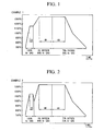
- a temperature of 700°C was achieved in an atmosphere of 100% Ar gas, and then the temperature was increased to 1150°C, which was maintained for one hour. Thereafter, in an atmosphere of argon-based 1% oxygen, the temperature was increased to 1350°C, which was maintained for four hours. The temperature was maintained for another four hours in an atmosphere of 70% oxygen and was then decreased to 700°C.
- the surface oxide films were removed in a HF aqueous solution and subjected to SC-1 cleaning to produce final SIMOX products.
- SIMOX substrates are grouped in Example 1.
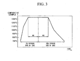
- Example 2 The same substrates as those three types in Example 1 were prepared. Oxygen ions were implanted into these three types of substrates under the same conditions as those in Example 1. Next, as shown in FIG. 2 , a temperature of 700°C was achieved in an atmosphere of 100% Ar gas, and then the temperature was increased to 1150°C, which was maintained for one hour. Thereafter, the temperature was decreased to 1000°C. Thereafter, in an atmosphere of argon-based 1% oxygen, the temperature was increased to 1350°C, which was maintained for four hours. The temperature was maintained for another four hours in an atmosphere of 70% oxygen and was then decreased to 700°C. Subsequently, the surface oxide films were removed in an HF aqueous solution and subjected to SC-1 cleaning to produce final SIMOX products. These SIMOX substrates are grouped in Example 2.
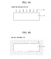
- Example 1 The same substrates as those three types in Example 1 were prepared. Oxygen ions were implanted into these three types of substrates under the same conditions as those in Example 1. Next, as shown in FIG. 3 , a temperature of 700°C was achieved, and then, in an atmosphere of argon-based 1% oxygen, the temperature was increased to 1350°C, which was maintained for four hours. The temperature was maintained for another four hours in an atmosphere of 70% oxygen and was then decreased to 700°C. Subsequently, the surface oxide films were removed in an HF aqueous solution and subjected to SC-1 cleaning to produce final SIMOX products. These SIMOX substrates are grouped in Comparative Example 1.
- Example 1 The substrates (1) to (3) in Example 1, Example 2, and Comparative Example 1 were checked using a surface-defect detection apparatus. The results are as described below.
- Example 1 measurements of the haze level were in a variation of about 1 ppb to 1020 ppb for all samples in the heat treatment furnace, although all substrates (1) to (3) had 0.3 to 0.5 pits per cm 2 . In particular, at the lower portions of the boat, the more significant degradation of haze was observed.
- Example 2 all substrates (1) to (3) had 0.3 to 0.5 pits per cm 2 , and measurements of the haze level were in a variation of about 1 ppb to 5 ppb for all samples. These measurements are equivalent to those of the conventional SIMOX product.
- this invention allows a SIMOX substrate based on a low-cost substrate to exhibit the same level of quality as that of a SIMOX substrate based on a costly substrate.
- an inner-wall oxide film of crystal defects resulting from heat treatment in an atmosphere of non-oxidizing gas, particularly void defects called grown-in defects, is dissolved, and thereafter grown-in defects adjacent to the surface can be reduced and eliminated by drawing upon a gap-filling effect by diffusion of interstitial silicon atoms in void defects where the inner-wall oxide film has been removed.
Landscapes
- Crystals, And After-Treatments Of Crystals (AREA)
- Element Separation (AREA)
Abstract
Applications Claiming Priority (2)
| Application Number | Priority Date | Filing Date | Title |
|---|---|---|---|
| JP2004211127A JP4706199B2 (ja) | 2004-07-20 | 2004-07-20 | Simox基板の製造方法 |
| PCT/JP2005/013259 WO2006009148A1 (ja) | 2004-07-20 | 2005-07-19 | Simox基板の製造方法 |
Publications (3)
| Publication Number | Publication Date |
|---|---|
| EP1786023A1 EP1786023A1 (en) | 2007-05-16 |
| EP1786023A4 EP1786023A4 (en) | 2008-08-13 |
| EP1786023B1 true EP1786023B1 (en) | 2011-11-16 |
Family
ID=35785256
Family Applications (1)
| Application Number | Title | Priority Date | Filing Date |
|---|---|---|---|
| EP05762053A Expired - Fee Related EP1786023B1 (en) | 2004-07-20 | 2005-07-19 | Simox substrate manufacturing method |
Country Status (7)
| Country | Link |
|---|---|
| US (1) | US7560363B2 (ja) |
| EP (1) | EP1786023B1 (ja) |
| JP (1) | JP4706199B2 (ja) |
| KR (1) | KR100834231B1 (ja) |
| CN (1) | CN100501922C (ja) |
| TW (1) | TWI270959B (ja) |
| WO (1) | WO2006009148A1 (ja) |
Families Citing this family (7)
| Publication number | Priority date | Publication date | Assignee | Title |
|---|---|---|---|---|
| JP4706199B2 (ja) * | 2004-07-20 | 2011-06-22 | 株式会社Sumco | Simox基板の製造方法 |
| JP5343371B2 (ja) * | 2008-03-05 | 2013-11-13 | 株式会社Sumco | シリコン基板とその製造方法 |
| JP5561918B2 (ja) * | 2008-07-31 | 2014-07-30 | グローバルウェーハズ・ジャパン株式会社 | シリコンウェーハの製造方法 |
| JP5498678B2 (ja) * | 2008-09-25 | 2014-05-21 | グローバルウェーハズ・ジャパン株式会社 | シリコンウェーハの製造方法 |
| JP2010135538A (ja) * | 2008-12-04 | 2010-06-17 | Sumco Corp | 貼り合わせウェーハの製造方法 |
| US8492290B2 (en) * | 2011-06-21 | 2013-07-23 | International Business Machines Corporation | Fabrication of silicon oxide and oxynitride having sub-nanometer thickness |
| JP2014168090A (ja) * | 2014-04-24 | 2014-09-11 | Globalwafers Japan Co Ltd | シリコンウェーハの製造方法 |
Family Cites Families (23)
| Publication number | Priority date | Publication date | Assignee | Title |
|---|---|---|---|---|
| JPS6472533A (en) * | 1987-09-11 | 1989-03-17 | Nippon Telegraph & Telephone | Manufacture of single crystal semiconductor substrate |
| JPH01122019A (ja) * | 1987-11-06 | 1989-05-15 | Hitachi Maxell Ltd | 信号入り磁気テープ |
| JPH05335301A (ja) * | 1992-06-03 | 1993-12-17 | Oki Electric Ind Co Ltd | シリコン酸化膜の形成方法 |
| JPH07193072A (ja) * | 1993-12-27 | 1995-07-28 | Nec Corp | 半導体基板の製造方法 |
| JP3995286B2 (ja) | 1996-04-26 | 2007-10-24 | Sumco Techxiv株式会社 | Simox基板の製造方法 |
| JP3583870B2 (ja) | 1996-08-19 | 2004-11-04 | 新日本製鐵株式会社 | 半導体基板及びその製造方法 |
| DE19637182A1 (de) * | 1996-09-12 | 1998-03-19 | Wacker Siltronic Halbleitermat | Verfahren zur Herstellung von Halbleiterscheiben aus Silicium mit geringer Defektdichte |
| JPH1140512A (ja) * | 1997-07-22 | 1999-02-12 | Komatsu Denshi Kinzoku Kk | 半導体基板の製造方法 |
| JPH11220019A (ja) * | 1998-02-02 | 1999-08-10 | Nippon Steel Corp | Soi基板およびその製造方法 |
| WO1999039380A1 (en) * | 1998-02-02 | 1999-08-05 | Nippon Steel Corporation | Soi substrate and method for manufacturing the same |
| TW469643B (en) * | 1998-09-04 | 2001-12-21 | Canon Kk | Process for producing semiconductor substrate |
| JP2001223220A (ja) * | 2000-02-08 | 2001-08-17 | Mitsubishi Materials Silicon Corp | 半導体ウェーハの熱処理方法及び半導体ウェーハ |
| TWI313059B (ja) * | 2000-12-08 | 2009-08-01 | Sony Corporatio | |
| US6734762B2 (en) * | 2001-04-09 | 2004-05-11 | Motorola, Inc. | MEMS resonators and method for manufacturing MEMS resonators |
| US6632694B2 (en) * | 2001-10-17 | 2003-10-14 | Astralux, Inc. | Double heterojunction light emitting diodes and laser diodes having quantum dot silicon light emitters |
| US6927422B2 (en) * | 2002-10-17 | 2005-08-09 | Astralux, Inc. | Double heterojunction light emitting diodes and laser diodes having quantum dot silicon light emitters |
| US6927146B2 (en) * | 2003-06-17 | 2005-08-09 | Intel Corporation | Chemical thinning of epitaxial silicon layer over buried oxide |
| JP2005340348A (ja) * | 2004-05-25 | 2005-12-08 | Sumco Corp | Simox基板の製造方法及び該方法により得られるsimox基板 |
| JP4706199B2 (ja) * | 2004-07-20 | 2011-06-22 | 株式会社Sumco | Simox基板の製造方法 |
| JP4815352B2 (ja) * | 2004-09-16 | 2011-11-16 | 株式会社日立国際電気 | 熱処理装置、基板の製造方法、基板処理方法、及び半導体装置の製造方法 |
| WO2007007386A1 (ja) * | 2005-07-11 | 2007-01-18 | Sumitomo Mitsubishi Silicon Corporation | Simox基板の製造方法及び該方法により得られるsimox基板 |
| CN101292341A (zh) * | 2005-08-26 | 2008-10-22 | Memc电子材料有限公司 | 绝缘体上应变硅结构的制造方法 |
| JP2007227424A (ja) * | 2006-02-21 | 2007-09-06 | Sumco Corp | Simoxウェーハの製造方法 |
-
2004
- 2004-07-20 JP JP2004211127A patent/JP4706199B2/ja not_active Expired - Fee Related
-
2005
- 2005-07-19 TW TW094124383A patent/TWI270959B/zh not_active IP Right Cessation
- 2005-07-19 WO PCT/JP2005/013259 patent/WO2006009148A1/ja not_active Ceased
- 2005-07-19 US US11/632,875 patent/US7560363B2/en not_active Expired - Fee Related
- 2005-07-19 CN CNB2005800246636A patent/CN100501922C/zh not_active Expired - Fee Related
- 2005-07-19 EP EP05762053A patent/EP1786023B1/en not_active Expired - Fee Related
- 2005-07-19 KR KR1020077003782A patent/KR100834231B1/ko not_active Expired - Fee Related
Also Published As
| Publication number | Publication date |
|---|---|
| JP4706199B2 (ja) | 2011-06-22 |
| TW200608515A (en) | 2006-03-01 |
| JP2006032752A (ja) | 2006-02-02 |
| CN1989592A (zh) | 2007-06-27 |
| TWI270959B (en) | 2007-01-11 |
| US7560363B2 (en) | 2009-07-14 |
| EP1786023A4 (en) | 2008-08-13 |
| EP1786023A1 (en) | 2007-05-16 |
| KR20070032823A (ko) | 2007-03-22 |
| WO2006009148A1 (ja) | 2006-01-26 |
| US20080090384A1 (en) | 2008-04-17 |
| CN100501922C (zh) | 2009-06-17 |
| KR100834231B1 (ko) | 2008-05-30 |
Similar Documents
| Publication | Publication Date | Title |
|---|---|---|
| JP3011178B2 (ja) | 半導体シリコンウェーハ並びにその製造方法と熱処理装置 | |
| JP3750526B2 (ja) | シリコンウエーハの製造方法及びシリコンウエーハ | |
| TWI553173B (zh) | An annealing wafer, an annealing wafer, and a method of manufacturing the device | |
| US7947571B2 (en) | Method for fabricating a semiconductor on insulator substrate with reduced Secco defect density | |
| WO2001017024A1 (en) | Fabrication method for pasted soi wafer and pasted soi wafer | |
| EP2199435A1 (en) | Annealed wafer and method for producing annealed wafer | |
| KR100947815B1 (ko) | Soi 웨이퍼의 제조 방법 및 soi 웨이퍼 | |
| KR100396609B1 (ko) | 반도체기판의처리방법 | |
| EP1313137A1 (en) | Method for manufacturing single-crystal silicon wafers | |
| EP1786023B1 (en) | Simox substrate manufacturing method | |
| KR100625822B1 (ko) | 실리콘 웨이퍼 및 그의 제조 방법 | |
| EP1347508B1 (en) | Method of heat treatment of silicon wafer doped with boron | |
| EP1298731B1 (en) | Simox substrate production process | |
| JP2007266059A (ja) | Simoxウェーハの製造方法 | |
| EP1906450A1 (en) | Process for producing simox substrate, and simox substrate produced by said process | |
| US20070020886A1 (en) | Method for reducing the trap density in a semiconductor wafer | |
| JP2000031079A (ja) | Soi基板の製造方法 | |
| US7160385B2 (en) | Silicon wafer and method for manufacturing the same | |
| US20250293073A1 (en) | Reclaimable donor substrates for use in preparing multiple silicon-on-insulator structures | |
| JPH08203913A (ja) | 半導体ウェーハの熱処理方法 | |
| JP2010027731A (ja) | Simoxウェーハの製造方法及びsimoxウェーハ | |
| US20130012008A1 (en) | Method of producing soi wafer | |
| JPH09116126A (ja) | Simoxウエハーおよびその製造方法 | |
| JP2008159868A (ja) | Simox基板の製造方法 | |
| JP2005286282A (ja) | Simox基板の製造方法及び該方法により得られるsimox基板 |
Legal Events
| Date | Code | Title | Description |
|---|---|---|---|
| PUAI | Public reference made under article 153(3) epc to a published international application that has entered the european phase |
Free format text: ORIGINAL CODE: 0009012 |
|
| 17P | Request for examination filed |
Effective date: 20070123 |
|
| AK | Designated contracting states |
Kind code of ref document: A1 Designated state(s): DE FR |
|
| DAX | Request for extension of the european patent (deleted) | ||
| RBV | Designated contracting states (corrected) |
Designated state(s): DE FR |
|
| A4 | Supplementary search report drawn up and despatched |
Effective date: 20080715 |
|
| 17Q | First examination report despatched |
Effective date: 20100921 |
|
| GRAP | Despatch of communication of intention to grant a patent |
Free format text: ORIGINAL CODE: EPIDOSNIGR1 |
|
| GRAS | Grant fee paid |
Free format text: ORIGINAL CODE: EPIDOSNIGR3 |
|
| GRAA | (expected) grant |
Free format text: ORIGINAL CODE: 0009210 |
|
| AK | Designated contracting states |
Kind code of ref document: B1 Designated state(s): DE FR |
|
| REG | Reference to a national code |
Ref country code: DE Ref legal event code: R096 Ref document number: 602005031242 Country of ref document: DE Effective date: 20120126 |
|
| PLBE | No opposition filed within time limit |
Free format text: ORIGINAL CODE: 0009261 |
|
| STAA | Information on the status of an ep patent application or granted ep patent |
Free format text: STATUS: NO OPPOSITION FILED WITHIN TIME LIMIT |
|
| 26N | No opposition filed |
Effective date: 20120817 |
|
| REG | Reference to a national code |
Ref country code: DE Ref legal event code: R097 Ref document number: 602005031242 Country of ref document: DE Effective date: 20120817 |
|
| PGFP | Annual fee paid to national office [announced via postgrant information from national office to epo] |
Ref country code: DE Payment date: 20130722 Year of fee payment: 9 |
|
| PGFP | Annual fee paid to national office [announced via postgrant information from national office to epo] |
Ref country code: FR Payment date: 20130722 Year of fee payment: 9 |
|
| REG | Reference to a national code |
Ref country code: DE Ref legal event code: R119 Ref document number: 602005031242 Country of ref document: DE |
|
| REG | Reference to a national code |
Ref country code: FR Ref legal event code: ST Effective date: 20150331 |
|
| PG25 | Lapsed in a contracting state [announced via postgrant information from national office to epo] |
Ref country code: DE Free format text: LAPSE BECAUSE OF NON-PAYMENT OF DUE FEES Effective date: 20150203 |
|
| REG | Reference to a national code |
Ref country code: DE Ref legal event code: R119 Ref document number: 602005031242 Country of ref document: DE Effective date: 20150203 |
|
| PG25 | Lapsed in a contracting state [announced via postgrant information from national office to epo] |
Ref country code: FR Free format text: LAPSE BECAUSE OF NON-PAYMENT OF DUE FEES Effective date: 20140731 |