EP1826816A1 - Halbleitervorrichtung, elektronische Vorrichtung und Herstellungsverfahren dafür - Google Patents
Halbleitervorrichtung, elektronische Vorrichtung und Herstellungsverfahren dafür Download PDFInfo
- Publication number
- EP1826816A1 EP1826816A1 EP06126262A EP06126262A EP1826816A1 EP 1826816 A1 EP1826816 A1 EP 1826816A1 EP 06126262 A EP06126262 A EP 06126262A EP 06126262 A EP06126262 A EP 06126262A EP 1826816 A1 EP1826816 A1 EP 1826816A1
- Authority
- EP
- European Patent Office
- Prior art keywords
- pad layer
- layer
- insulating layer
- semiconductor substrate
- lower pad
- Prior art date
- Legal status (The legal status is an assumption and is not a legal conclusion. Google has not performed a legal analysis and makes no representation as to the accuracy of the status listed.)
- Granted
Links
Images



Classifications
-
- H—ELECTRICITY
- H10—SEMICONDUCTOR DEVICES; ELECTRIC SOLID-STATE DEVICES NOT OTHERWISE PROVIDED FOR
- H10W—GENERIC PACKAGES, INTERCONNECTIONS, CONNECTORS OR OTHER CONSTRUCTIONAL DETAILS OF DEVICES COVERED BY CLASS H10
- H10W74/00—Encapsulations, e.g. protective coatings
- H10W74/10—Encapsulations, e.g. protective coatings characterised by their shape or disposition
- H10W74/131—Encapsulations, e.g. protective coatings characterised by their shape or disposition the semiconductor body being only partially enclosed
- H10W74/147—Encapsulations, e.g. protective coatings characterised by their shape or disposition the semiconductor body being only partially enclosed the encapsulations being multilayered
-
- H—ELECTRICITY
- H10—SEMICONDUCTOR DEVICES; ELECTRIC SOLID-STATE DEVICES NOT OTHERWISE PROVIDED FOR
- H10W—GENERIC PACKAGES, INTERCONNECTIONS, CONNECTORS OR OTHER CONSTRUCTIONAL DETAILS OF DEVICES COVERED BY CLASS H10
- H10W20/00—Interconnections in chips, wafers or substrates
- H10W20/01—Manufacture or treatment
- H10W20/031—Manufacture or treatment of conductive parts of the interconnections
- H10W20/069—Manufacture or treatment of conductive parts of the interconnections by forming self-aligned vias or self-aligned contact plugs
-
- H—ELECTRICITY
- H10—SEMICONDUCTOR DEVICES; ELECTRIC SOLID-STATE DEVICES NOT OTHERWISE PROVIDED FOR
- H10W—GENERIC PACKAGES, INTERCONNECTIONS, CONNECTORS OR OTHER CONSTRUCTIONAL DETAILS OF DEVICES COVERED BY CLASS H10
- H10W72/00—Interconnections or connectors in packages
- H10W72/01—Manufacture or treatment
- H10W72/012—Manufacture or treatment of bump connectors, dummy bumps or thermal bumps
- H10W72/01221—Manufacture or treatment of bump connectors, dummy bumps or thermal bumps using local deposition
- H10W72/01223—Manufacture or treatment of bump connectors, dummy bumps or thermal bumps using local deposition in liquid form, e.g. by dispensing droplets or by screen printing
-
- H—ELECTRICITY
- H10—SEMICONDUCTOR DEVICES; ELECTRIC SOLID-STATE DEVICES NOT OTHERWISE PROVIDED FOR
- H10W—GENERIC PACKAGES, INTERCONNECTIONS, CONNECTORS OR OTHER CONSTRUCTIONAL DETAILS OF DEVICES COVERED BY CLASS H10
- H10W72/00—Interconnections or connectors in packages
- H10W72/01—Manufacture or treatment
- H10W72/019—Manufacture or treatment of bond pads
- H10W72/01931—Manufacture or treatment of bond pads using blanket deposition
- H10W72/01933—Manufacture or treatment of bond pads using blanket deposition in liquid form, e.g. spin coating, spray coating or immersion coating
- H10W72/01935—Manufacture or treatment of bond pads using blanket deposition in liquid form, e.g. spin coating, spray coating or immersion coating by plating, e.g. electroless plating or electroplating
-
- H—ELECTRICITY
- H10—SEMICONDUCTOR DEVICES; ELECTRIC SOLID-STATE DEVICES NOT OTHERWISE PROVIDED FOR
- H10W—GENERIC PACKAGES, INTERCONNECTIONS, CONNECTORS OR OTHER CONSTRUCTIONAL DETAILS OF DEVICES COVERED BY CLASS H10
- H10W72/00—Interconnections or connectors in packages
- H10W72/01—Manufacture or treatment
- H10W72/019—Manufacture or treatment of bond pads
- H10W72/01931—Manufacture or treatment of bond pads using blanket deposition
- H10W72/01938—Manufacture or treatment of bond pads using blanket deposition in gaseous form, e.g. by CVD or PVD
-
- H—ELECTRICITY
- H10—SEMICONDUCTOR DEVICES; ELECTRIC SOLID-STATE DEVICES NOT OTHERWISE PROVIDED FOR
- H10W—GENERIC PACKAGES, INTERCONNECTIONS, CONNECTORS OR OTHER CONSTRUCTIONAL DETAILS OF DEVICES COVERED BY CLASS H10
- H10W72/00—Interconnections or connectors in packages
- H10W72/071—Connecting or disconnecting
- H10W72/072—Connecting or disconnecting of bump connectors
-
- H—ELECTRICITY
- H10—SEMICONDUCTOR DEVICES; ELECTRIC SOLID-STATE DEVICES NOT OTHERWISE PROVIDED FOR
- H10W—GENERIC PACKAGES, INTERCONNECTIONS, CONNECTORS OR OTHER CONSTRUCTIONAL DETAILS OF DEVICES COVERED BY CLASS H10
- H10W72/00—Interconnections or connectors in packages
- H10W72/071—Connecting or disconnecting
- H10W72/072—Connecting or disconnecting of bump connectors
- H10W72/07251—Connecting or disconnecting of bump connectors characterised by changes in properties of the bump connectors during connecting
-
- H—ELECTRICITY
- H10—SEMICONDUCTOR DEVICES; ELECTRIC SOLID-STATE DEVICES NOT OTHERWISE PROVIDED FOR
- H10W—GENERIC PACKAGES, INTERCONNECTIONS, CONNECTORS OR OTHER CONSTRUCTIONAL DETAILS OF DEVICES COVERED BY CLASS H10
- H10W72/00—Interconnections or connectors in packages
- H10W72/20—Bump connectors, e.g. solder bumps or copper pillars; Dummy bumps; Thermal bumps
-
- H—ELECTRICITY
- H10—SEMICONDUCTOR DEVICES; ELECTRIC SOLID-STATE DEVICES NOT OTHERWISE PROVIDED FOR
- H10W—GENERIC PACKAGES, INTERCONNECTIONS, CONNECTORS OR OTHER CONSTRUCTIONAL DETAILS OF DEVICES COVERED BY CLASS H10
- H10W72/00—Interconnections or connectors in packages
- H10W72/20—Bump connectors, e.g. solder bumps or copper pillars; Dummy bumps; Thermal bumps
- H10W72/221—Structures or relative sizes
-
- H—ELECTRICITY
- H10—SEMICONDUCTOR DEVICES; ELECTRIC SOLID-STATE DEVICES NOT OTHERWISE PROVIDED FOR
- H10W—GENERIC PACKAGES, INTERCONNECTIONS, CONNECTORS OR OTHER CONSTRUCTIONAL DETAILS OF DEVICES COVERED BY CLASS H10
- H10W72/00—Interconnections or connectors in packages
- H10W72/20—Bump connectors, e.g. solder bumps or copper pillars; Dummy bumps; Thermal bumps
- H10W72/241—Dispositions, e.g. layouts
-
- H—ELECTRICITY
- H10—SEMICONDUCTOR DEVICES; ELECTRIC SOLID-STATE DEVICES NOT OTHERWISE PROVIDED FOR
- H10W—GENERIC PACKAGES, INTERCONNECTIONS, CONNECTORS OR OTHER CONSTRUCTIONAL DETAILS OF DEVICES COVERED BY CLASS H10
- H10W72/00—Interconnections or connectors in packages
- H10W72/20—Bump connectors, e.g. solder bumps or copper pillars; Dummy bumps; Thermal bumps
- H10W72/251—Materials
- H10W72/252—Materials comprising solid metals or solid metalloids, e.g. PbSn, Ag or Cu
-
- H—ELECTRICITY
- H10—SEMICONDUCTOR DEVICES; ELECTRIC SOLID-STATE DEVICES NOT OTHERWISE PROVIDED FOR
- H10W—GENERIC PACKAGES, INTERCONNECTIONS, CONNECTORS OR OTHER CONSTRUCTIONAL DETAILS OF DEVICES COVERED BY CLASS H10
- H10W72/00—Interconnections or connectors in packages
- H10W72/20—Bump connectors, e.g. solder bumps or copper pillars; Dummy bumps; Thermal bumps
- H10W72/29—Bond pads specially adapted therefor
-
- H—ELECTRICITY
- H10—SEMICONDUCTOR DEVICES; ELECTRIC SOLID-STATE DEVICES NOT OTHERWISE PROVIDED FOR
- H10W—GENERIC PACKAGES, INTERCONNECTIONS, CONNECTORS OR OTHER CONSTRUCTIONAL DETAILS OF DEVICES COVERED BY CLASS H10
- H10W72/00—Interconnections or connectors in packages
- H10W72/90—Bond pads, in general
- H10W72/921—Structures or relative sizes of bond pads
- H10W72/923—Bond pads having multiple stacked layers
-
- H—ELECTRICITY
- H10—SEMICONDUCTOR DEVICES; ELECTRIC SOLID-STATE DEVICES NOT OTHERWISE PROVIDED FOR
- H10W—GENERIC PACKAGES, INTERCONNECTIONS, CONNECTORS OR OTHER CONSTRUCTIONAL DETAILS OF DEVICES COVERED BY CLASS H10
- H10W72/00—Interconnections or connectors in packages
- H10W72/90—Bond pads, in general
- H10W72/931—Shapes of bond pads
- H10W72/934—Cross-sectional shape, i.e. in side view
-
- H—ELECTRICITY
- H10—SEMICONDUCTOR DEVICES; ELECTRIC SOLID-STATE DEVICES NOT OTHERWISE PROVIDED FOR
- H10W—GENERIC PACKAGES, INTERCONNECTIONS, CONNECTORS OR OTHER CONSTRUCTIONAL DETAILS OF DEVICES COVERED BY CLASS H10
- H10W72/00—Interconnections or connectors in packages
- H10W72/90—Bond pads, in general
- H10W72/941—Dispositions of bond pads
- H10W72/9415—Dispositions of bond pads relative to the surface, e.g. recessed, protruding
-
- H—ELECTRICITY
- H10—SEMICONDUCTOR DEVICES; ELECTRIC SOLID-STATE DEVICES NOT OTHERWISE PROVIDED FOR
- H10W—GENERIC PACKAGES, INTERCONNECTIONS, CONNECTORS OR OTHER CONSTRUCTIONAL DETAILS OF DEVICES COVERED BY CLASS H10
- H10W72/00—Interconnections or connectors in packages
- H10W72/90—Bond pads, in general
- H10W72/941—Dispositions of bond pads
- H10W72/942—Dispositions of bond pads relative to underlying supporting features, e.g. bond pads, RDLs or vias
-
- H—ELECTRICITY
- H10—SEMICONDUCTOR DEVICES; ELECTRIC SOLID-STATE DEVICES NOT OTHERWISE PROVIDED FOR
- H10W—GENERIC PACKAGES, INTERCONNECTIONS, CONNECTORS OR OTHER CONSTRUCTIONAL DETAILS OF DEVICES COVERED BY CLASS H10
- H10W72/00—Interconnections or connectors in packages
- H10W72/90—Bond pads, in general
- H10W72/951—Materials of bond pads
- H10W72/952—Materials of bond pads comprising metals or metalloids, e.g. PbSn, Ag or Cu
Definitions
- This invention generally relates to a semiconductor device, an electronic device and a fabrication method of the same, and in particular, relates a semiconductor device and an electronic device having a pad electrode and a fabrication method of the same.
- a semiconductor device using a high frequency wave such as a microwave or a milliwave is used in an electronic device such as a cellular phone or a satellite receiver.
- a semiconductor substrate semiconductor chip having an active element or a passive element is mounted on a package or on a mounting substrate in the electronic device.
- a pad electrode is provided on the semiconductor substrate. The pad electrode is used for electronic connection between the semiconductor chip and the package or the mounting substrate.
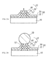
- FIG. 1A and FIG. 1B illustrate a structure of the pad electrode of a semiconductor chip in accordance with a conventional embodiment.
- a first pad layer 22 is provided on a semiconductor substrate 10.
- a first insulating layer 32 is provided on the semiconductor substrate 10 and on a surrounding of the first pad layer 22.
- a second pad layer 24 is provided on the first pad layer 22.
- a lower pad layer 20 is composed of the first pad layer 22 and the second pad layer 24.
- a second insulating layer 38 is provided on the first insulating layer 32 and on a surrounding of the lower pad layer 20.
- An upper pad layer 40 is provided on the lower pad layer 20.
- a pad electrode 12 is composed of the lower pad layer 20 and the upper pad layer 40. As shown in FIG.
- a connecting terminal 50 is provided on the upper pad layer 40.
- the connecting terminal 50 is composed of a solder for connecting the pad electrode electrically to a package or a mounting substrate on which the semiconductor Chip is mounted.
- Japanese Patent Application Publication No. 9-205096 discloses a case where the lower pad layer 20 is composed of a layer.
- the first pad layer 22 and the second pad layer 24 of the lower pad layer 20 are used for a wiring of the semiconductor chip.
- a metal having a low electrical resistance such as Au is used for the first pad layer 22 and the second pad layer 24.
- a bump such as a solder is used as the connecting terminal 50 in order to connect the pad electrode electrically to a package or a mounting substrate.
- a material acting as a barrier layer is used as the upper pad layer 40 in order to prevent the diffusion of a material of the lower pad layer 20 into the connecting terminal 50.
- FIG. 2A and FIG. 2B illustrate a case where the pad electrode 12 is formed to be small in order to reduce the capacity of the pad electrode 12 in the conventional embodiment.
- a width B of a recess on a top face of the upper pad layer 40 is smaller than a width A of a recess on a top face of the upper pad layer 40 shown in FIG. 1A.
- the recess is deep and has a small width, in a case where the lower pad layer 20 is composed of the first pad layer 22 and the second pad layer 24, and the first insulating layer 32 and the second insulating layer 38 cover the surrounding of the first pad layer 22 and the second pad layer 24, respectively.
- the width B is approximately 10 ⁇ m, in a case where a height of the pad electrode 12 is less than 50 ⁇ m and the height of the upper pad layer 40 is 10 ⁇ m to 20 ⁇ m in order to obtain a barrier property and relax a stress.
- a void 52 is formed in the recess when the connecting terminal 50 is formed on the upper pad layer 40 with a printing method (metal mask).
- Such a void 52 may make a high electrical resistance between the upper pad layer 40 and the connecting terminal 50. That is, impedance is increased when a high frequency wave is input or output through the pad electrode 12 and the connecting terminal 50. And the impedance causes a high frequency wave loss.
- a contact area between the upper pad layer 40 and the connecting terminal 50 is reduced when the area of the pad electrode 12 is reduced. And the adherence intensity between the upper pad layer 40 and the connecting terminal 50 is reduced. The adherence intensity between the upper pad layer 40 and the connecting terminal 50 is further reduced when the void 52 is formed as shown in FIG. 2B. It is thus necessary to enlarge the upper region of the pad electrode.
- the present invention provides a semiconductor device, an electronic device and a fabrication method thereof in which adherence intensity between a pad electrode and a connecting terminal is improved even in a case where a capacity of a pad electrode is reduced and the connecting terminal is provided on an upper pad layer.
- a semiconductor device including a lower pad layer, an insulating layer and an upper pad layer.
- the lower pad layer is provided on a semiconductor substrate.
- the insulating layer is away from a surrounding of the lower pad layer so that a space having a recess on a surface between the lower pad layer and the insulating layer is formed.
- the upper pad layer covers over the lower pad layer and the space, extends to an upper face of the insulating layer, and has an area larger than that of the lower pad layer.
- an electronic device including a lower pad layer, an insulating layer, an upper pad layer and a mount portion.
- the lower pad layer is provided on a semiconductor substrate.
- the insulating layer is away from a surrounding of the lower pad layer so that a space having a recess on a surface between the lower pad layer and the insulating layer is formed.
- the upper pad layer covers over the lower pad layer and the space, extends to an upper face of the insulating layer, and has an area larger than that of the lower pad layer.
- the semiconductor substrate is mounted on the mount portion.
- a fabrication method of a semiconductor device includes forming a lower pad layer on a semiconductor substrate, forming an insulating and forming an upper pad layer.
- the insulating layer is away from a surrounding of the lower pad layer so that a space having a recess on a surface between the lower pad layer and the insulating layer is formed.
- the upper pad layer covers over the lower pad layer and the space, extends to an upper face of the insulating layer, and has an area larger than that of the lower pad layer.
- a fabrication method of an electronic device includes forming a lower pad layer on a semiconductor substrate, forming an insulating layer, forming an upper pad layer and mounting the semiconductor substrate on a mount portion.
- the insulating layer is away from a surrounding of the lower pad layer so that a space having a recess on a surface between the lower pad layer and the insulating layer is formed.
- the upper pad layer covers over the lower pad layer and the space, extends to an upper face of the insulating layer, and has an area larger than that of the lower pad layer.
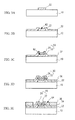
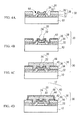
- FIG. 3A through FIG. 4D illustrate a cross sectional view showing a fabrication process of a semiconductor device in accordance with a first embodiment.
- a first pad layer 22 is formed on a semiconductor substrate 10 composed of GaAs, Si, SiC, GaN, InP or sapphire with an evaporation method or the like.
- the first pad layer 22 is, for example, composed of Ti/Au layer in which Ti layer and an Au layer is layered in order from the semiconductor substrate 10.
- the first pad layer 22 acts as an electrode of a transistor formed on the semiconductor substrate 10.
- a first insulating layer 32 is formed on the semiconductor substrate 10 and the first pad layer 22.
- the first insulating layer 32 is, for example, composed of a nonphotosensitive polyimide.
- An opening 62 is formed around a center ot the first insulating layer 32 on the first pad layer 22. That is, the first insulating layer 32 covers a part of an upper face of the first pad layer 22.
- a second pad layer 24 composed of a Ti/Au layer or the like is formed on the first pad layer 22 with an evaporation method. And the second pad layer 24 is electrically coupled to the first pad layer 22 through the opening 62 of the first insulating layer 32. The first pad layer 22 and the second pad layer 24 form a lower pad layer 20.
- a third insulating layer 34 composed of silicon nitride or the like is formed on the first insulating layer 32 and the lower pad layer 20.
- a photosensitive polyimide resin is coated on the third insulating layer 34.
- a fourth insulating layer 36 having an opening around the lower pad layer 20 is formed with exposure/development.
- the third insulating layer 34 is etched with use of the fourth insulating layer 36 for a mask. And the upper face of the second pad layer 24 is exposed.
- the third insulating layer 34 and the fourth insulating layer 36 form a second insulating layer 38.
- the lower pad layer 20 is surrounded by the first insulating layer 32 and the second insulating layer 38.
- a protective layer 30 is formed from the first insulating layer 32 and the second insulating layer 38.
- the protective layer 30 is approximately as tall as the lower pad layer 20.
- the second insulating layer 38 is arranged at a given interval from the lower pad layer 20. That is, the second insulating layer 38 is away from the lower pad layer 20.
- the second insulating layer 38 and the lower pad layer 20 form a space 64.
- the space 64 has a recess on an area between the second insulating layer 38 and the lower pad layer 20, the area being on the first insulating layer 32.
- a seed metal layer 42 is formed on the protective layer 30 and the lower pad layer 20.
- the seed metal layer 42 is composed of a layer or the like and is for plating.
- a plated layer 44 is formed on the seed metal layer 42 and above the lower pad layer 20 and the second insulating layer 38 with a plating method.
- the plated layer 44 is, for example, composed of a Ni layer.
- a cover layer 46 is formed so as to cover the plated layer 44.
- the cover layer 46 is, for example, composed of a Ti/Au layer. That is, a metal layer is formed on a top face of an upper pad layer 40. A part of the seed metal layer 42 and the cover layer 46 is etched, the part being except for an area to be the upper pad layer 40.
- the upper pad layer 40 is formed on the lower pad layer 20 and the protective layer 30, the upper pad layer 40 being composed of the seed metal layer 42, the plated layer 44 and the cover layer 46.
- the upper pad layer 40 covers over the lower pad layer 20 and the space 64, and extends to an upper face of the second insulating layer 38.
- the upper pad layer 40 is formed so as to cover an upper face of the lower pad layer 20 and a side face and a bottom face of the space 64.
- a semiconductor device 80 is fabricated.
- a connecting terminal 50 composed of a solder is formed on the upper pad layer 40 with a printing method.
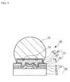
- the lower pad layer 20 is formed on the semiconductor substrate 10 as shown in FIG. 5.
- the second insulating layer 38 is formed on the semiconductor substrate 10 so as to be away from the surrounding of the lower pad layer 20.
- the space (the space 64 in FIG. 4A) having a recess between the second insulating layer 38 and the lower pad layer 20 is formed.
- the upper pad layer 40 covers over the lower pad layer 20 and the space 64.
- the upper pad layer 40 extends to an upper face of the second insulating layer 38.
- the upper pad layer 40 has an area larger than that of the lower pad layer 20.
- the upper pad layer 40 is, for example, 100 ⁇ m in width and 100 ⁇ m in length.
- the lower pad layer 20 is, for example, 50 ⁇ m in width and 50 ⁇ m in length.
- the contact area between the lower pad layer 20 and the semiconductor substrate 10 is a small area that is 50 ⁇ m in width and 50 ⁇ m in length. And the capacity of a pad electrode 12 is reduced. Particularly in a semiconductor device using a high frequency wave, it is necessary that the area of the pad electrode 12 contacting to the semiconductor substrate 10 is smaller than an area that is 100 ⁇ m in width and 100 ⁇ m in length and is preferably smaller than an area that is 50 ⁇ m in width and 50 ⁇ m in length.
- the contact area between the upper pad layer 40 and the connecting terminal 50 is a large area that is 100 ⁇ m in width and 100 ⁇ m in length. And the adherence intensity between the upper pad layer 40 and the connecting terminal 50 is improved.
- the upper pad layer 40 covers over the lower pad layer 20 and the space 64 and extends to the upper face of the second insulating layer 38 that is an insulating layer away from the surrounding of the lower pad layer 20. That is, the second insulating layer 38 is not provided above the surrounding area of the lower pad layer 20.
- the upper pad layer 40 is formed so as to contact to whole of the upper face of the lower pad layer 20. It is thus possible to restrain that a recess shown in FIG. 2A is formed on the upper face of the upper pad layer 40. Therefore, a void 52 shown in FIG. 2B is not formed and it is possible to restrain that the impedance of the pad electrode 12 and the connecting terminal 50 increases.
- a contact area between the upper pad layer 40 and the second insulating layer 38 and the lower pad layer 20 is increased because the space 64 is provided. And the adherence intensity between the upper pad layer 40 and the second insulating layer 38 and the lower pad layer 20 is improved. It is preferable that a material and a composition of the second insulating layer 38 are selected according to the adherence between the upper pad layer 40 and the second insulating layer 38.
- the first embodiment it is possible to enlarge a range of selection of the material and the composition of the second insulating layer 38, because the adherence intensity between the upper pad layer 40 and the second insulating layer 38 and the lower pad layer 20 is increased. Further, a recess 54 is formed on the upper face of the upper pad layer 40 above the space 64. Therefore, the adherence intensity between the pad electrode 12 and the connecting terminal 50 is improved.
- the upper face and the side face of the upper pad layer 40 are covered with Au.
- the connecting terminal 50 is composed of a solder
- the adherence intensity between the pad electrode 12 and the connecting terminal 50 is further increased.
- the adherence intensity between the pad electrode 12 and the connecting terminal 50 is further increased because the connecting terminal 50 is provided on the side face of the upper pad layer 40 as shown in FIG. 5.
- An area of the upper face of the upper pad layer 40 is larger than that of the bottom face of the lower pad layer 20. That is, the area of the upper face of the upper pad layer 40 is larger than that of the lower pad layer 20 that contacts to the semiconductor substrate 10. And the area of the upper pad layer 40 contacting to the connecting terminal 50 is larger than that of the lower pad layer 20 contacting to the semiconductor substrate 10. It is therefore possible to reduce the capacity of the pad electrode 12 and is possible to obtain the adherence intensity between the pad electrode 12 and the connecting terminal 50.
- the upper face of the lower pad layer 20 is approximately as high as the upper face of the protective layer 30. In this case, it is possible to restrain that a recess as shown in FIG. 2A is formed on the upper pad layer 40. It is therefore possible to further restrain that the void 52 shown in FIG. 2B is formed. Therefore, the upper face of the lower pad layer 20 is approximately as high as the upper face of the protective layer 30 so that the void 52 is not formed. In a case where the upper face of the protective layer 30 is higher than that of the lower pad layer 20 by more than 3 ⁇ m, the void 52 tends to be formed.
- the solder tends to run off during the mounting. It is preferable that the differential between the heights of the upper face of the protective layer 30 and the lower pad layer 20 is less than 3 ⁇ m, in the case where the upper face of the lower pad layer 20 is approximately as high as the upper face of the protective layer 30.
- the lower pad layer 20 includes the first pad layer 22 provided on the semiconductor substrate 10 and the second pad layer 24 provided on the first pad layer 22.
- the first insulating layer 32 (the lower insulating layer) is provided between the semiconductor substrate 10 and the second insulating layer 38 and covers a part of the upper face of the first pad layer 22.
- a recess tends to be formed on an upper face af the second pad layer 24, because the first insulating layer 32 is formed on the surrounding area of the first pad layer 22.
- a recess shown in FIG. 2A tends to be formed on the upper face of the upper pad layer 40 when the area of the pad electrode 12 is reduced.
- the void 52 shown in FIG. 2B tends to be formed between the upper pad layer 40 and the connecting terminal 50.
- FIG. 6 illustrates a cross sectional view of a semiconductor device in accordance with another example of the first embodiment.
- a lower pad layer 120 composed of a Ti/Au layer or the like is provided on a semiconductor substrate 110.
- An insulating layer 130 composed of a silicon nitride layer or the like is provided on the semiconductor substrate 110. The insulating layer 130 is away from a surrounding of the lower pad layer 120.
- a space 164 having a recess on a surface between the lower pad layer 120 and the insulating layer 130 is formed.
- An upper pad layer 140 is, for example, composed of an Au/Ni/Au layer.
- the upper pad layer 140 covers over the lower pad layer 120 and the space 164 and extends to an upper face of the insulating layer 130.
- the upper pad layer 140 has an area larger than that of the lower pad layer 120.
- the upper pad layer 140 and the lower pad layer 120 form a pad electrode 112. In this example, it is possible to obtain the same advantage as the first embodiment.
- the insulating layer arranged to be away from the surrounding of the lower pad layer 20 or 120 may be the second insulating layer 38 composed of two insulating layers or the insulating layer 130 in the example composed of one layer.
- the first insulating layer 32 may be provided between the second insulating layer 38 away from the surrounding of the lower pad layer 20 and the semiconductor substrate 10.
- the first insulating layer 32 may be provided on the semiconductor substrate 10 directly, similarly to the insulating layer 130.
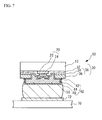
- a second embodiment is an example of an electronic device in which the semiconductor device 80 in accordance with the first embodiment is mounted.
- the connecting terminal 50 in accordance with the second embodiment is coupled to a pad electrode 72 that is provided on a mount portion 70 and is composed of Au or the like. That is, the semiconductor substrate 10 of the semiconductor device 80 is mounted face down on the mount portion 70 with the connecting terminal 50.
- the mount portion 70 may be a package composed of ceramics or a mount substrate such as a printing substrate.
- the semiconductor device 80 may be mounted flip chip, although the semiconductor device 80 is mounted face down in the second embodiment.
- a die shear intensity of the semiconductor device 80 mounted on the mount portion 70 is measured, in a case where the mount portion 70 is a package, the connecting terminal 50 is composed of a solder and the plated layer 44 is composed of Ni having a thickness of more than 3 ⁇ m. Open circles in FIG. 8 show the results.
- FIG. 8 illustrates a die shear intensity of the semiconductor device 80 with respect to the junction area between the solder of the connecting terminal 50 and the upper pad layer 40. When the junction area is enlarged, the die shear intensity increases, It is necessary that the junction area is more than 10, 000 ⁇ m 2 , if the die shear intensity is more than 30 N.
- the junction area between the solder and the upper pad layer 40 is a large area that is 100 ⁇ m in width and 100 ⁇ m in length as shown in FIG. 8, if the semiconductor device 80 in accordance with the first embodiment is used. Therefore the die shear intensity is increased.
- the contact area between the lower pad layer 20 and the semiconductor substrate 10 (or a semiconductor layer of the semiconductor substrate) is small area that is 50 ⁇ m in width and 50 ⁇ m in length as in the case of the first embodiment. Therefore, the capacity of the pad electrode 12 is reduced.
- the second embodiment is a case where the connecting terminal 50 is formed on the pad electrode 12 of the semiconductor device 80 and the semiconductor device 80 is mounted on the mount portion 70.
- the connecting terminal 50 may be formed on the mount portion 70 and the semiconductor substrate 10 may be mounted on the mount portion 70 with the connecting terminal 50.
- the semiconductor device of another example of the first embodiment may be mounted on the mount portion 70.
- the lower pad layer 20 may be composed of a metal except for Au.
- the lower pad layer 20 acts as an electrode and a wire of an element provided on the semiconductor substrate 10.
- the lower pad layer 20 is composed of a low-resistivity metal.
- the upper pad layer 40 may be composed of a metal except for Ni.
- the upper pad layer 40 may be composed of copper.
- the upper pad layer 40 is composed of a metal acting as a barrier layer between the connecting terminal 50 and the lower pad layer 20.
- the thickness of the Ni layer acting as a barrier layer of the solder is more than 3 ⁇ m.
- the thickness of the upper pad layer 40 is more than 10 ⁇ m.
- the insulating layers 32, 34 and 36 and the insulating layer 130 may be composed of an inorganic layer such as silicon nitride layer or an organic layer such as polyimid resin layer.
- the connecting terminal 50 may be composed of a metal except for the solder.
- the connecting terminal 50 is composed of a metal to be electrically coupled to the mount portion 70.
Landscapes
- Internal Circuitry In Semiconductor Integrated Circuit Devices (AREA)
- Wire Bonding (AREA)
Applications Claiming Priority (1)
| Application Number | Priority Date | Filing Date | Title |
|---|---|---|---|
| JP2006054174A JP4750586B2 (ja) | 2006-02-28 | 2006-02-28 | 半導体装置および電子装置並びにその製造方法 |
Publications (3)
| Publication Number | Publication Date |
|---|---|
| EP1826816A1 true EP1826816A1 (de) | 2007-08-29 |
| EP1826816B1 EP1826816B1 (de) | 2015-02-18 |
| EP1826816B8 EP1826816B8 (de) | 2015-05-06 |
Family
ID=38171330
Family Applications (1)
| Application Number | Title | Priority Date | Filing Date |
|---|---|---|---|
| EP20060126262 Ceased EP1826816B8 (de) | 2006-02-28 | 2006-12-15 | Halbleitervorrichtung, elektronische Vorrichtung und Herstellungsverfahren dafür |
Country Status (4)
| Country | Link |
|---|---|
| US (1) | US7821134B2 (de) |
| EP (1) | EP1826816B8 (de) |
| JP (1) | JP4750586B2 (de) |
| TW (1) | TWI329901B (de) |
Families Citing this family (4)
| Publication number | Priority date | Publication date | Assignee | Title |
|---|---|---|---|---|
| JP2012243984A (ja) * | 2011-05-20 | 2012-12-10 | Fujikura Ltd | 半導体装置および半導体装置の製造方法 |
| JP2013229491A (ja) * | 2012-04-26 | 2013-11-07 | Kyocera Corp | 電極構造、半導体素子、半導体装置、サーマルヘッドおよびサーマルプリンタ |
| US20150318254A1 (en) * | 2013-12-17 | 2015-11-05 | Oracle International Corporation | Electroplated solder with eutectic chemical composition |
| CN109920739A (zh) * | 2016-08-19 | 2019-06-21 | 华为技术有限公司 | 一种半导体封装结构及其制造方法 |
Citations (8)
| Publication number | Priority date | Publication date | Assignee | Title |
|---|---|---|---|---|
| EP0104079A2 (de) * | 1982-09-20 | 1984-03-28 | International Business Machines Corporation | Kontaktstruktur für integrierte Schaltung |
| DE19745575A1 (de) * | 1996-10-16 | 1998-04-30 | Casio Computer Co Ltd | Struktur einer Anschlußelektrode und Verfahren für ihre Bildung |
| US20010039113A1 (en) * | 1996-02-02 | 2001-11-08 | Guy Blalock | Method for forming a semiconductor connection with a top surface having an enlarged recess |
| US6323528B1 (en) * | 1991-03-06 | 2001-11-27 | Semiconductor Energy Laboratory Co,. Ltd. | Semiconductor device |
| US20020090786A1 (en) * | 2001-01-06 | 2002-07-11 | Kim Young-Pil | Methods of manufacturing integrated circuit devices having reduced contact resistance between a substrate and a contact pad while maintaining separation of the substrate and the contact pad and integrated circuit devices formed thereby |
| US6586273B2 (en) | 2000-12-12 | 2003-07-01 | Fujitsu Limited | Semiconductor device manufacturing method having a step of applying a copper foil on a substrate as a part of a wiring connecting an electrode pad to a mounting terminal |
| US20050130388A1 (en) * | 2003-12-15 | 2005-06-16 | Moon Sik Suh | Method for forming mos transistor |
| US20050142841A1 (en) * | 2003-12-31 | 2005-06-30 | Dongbuanam Semiconductor Inc. | Method for forming metal pattern to reduce contact resistivity with interconnection contact |
Family Cites Families (16)
| Publication number | Priority date | Publication date | Assignee | Title |
|---|---|---|---|---|
| JPH03265140A (ja) * | 1990-03-15 | 1991-11-26 | Fujitsu Ltd | 半導体装置およびその製造方法 |
| TW247373B (en) | 1994-10-11 | 1995-05-11 | Chau-Jyh Day | Silicon bridge rectifier |
| JPH09205096A (ja) | 1996-01-24 | 1997-08-05 | Toshiba Corp | 半導体素子およびその製造方法および半導体装置およびその製造方法 |
| US7759803B2 (en) * | 2001-07-25 | 2010-07-20 | Rohm Co., Ltd. | Semiconductor device and method of manufacturing the same |
| JP3538170B2 (ja) * | 2001-09-11 | 2004-06-14 | 松下電器産業株式会社 | 半導体装置及びその製造方法 |
| JP2003100766A (ja) * | 2001-09-27 | 2003-04-04 | Sanyo Electric Co Ltd | 半導体装置 |
| JP2003347338A (ja) * | 2002-05-29 | 2003-12-05 | Sharp Corp | 半導体装置 |
| US6960828B2 (en) * | 2002-06-25 | 2005-11-01 | Unitive International Limited | Electronic structures including conductive shunt layers |
| JP3590039B2 (ja) * | 2002-07-24 | 2004-11-17 | 沖電気工業株式会社 | 半導体装置及びその製造方法 |
| JP3970150B2 (ja) * | 2002-10-16 | 2007-09-05 | 三洋電機株式会社 | ボンディングパッド及びその形成方法 |
| JP2004214594A (ja) * | 2002-11-15 | 2004-07-29 | Sharp Corp | 半導体装置およびその製造方法 |
| US7042065B2 (en) * | 2003-03-05 | 2006-05-09 | Ricoh Company, Ltd. | Semiconductor device and method of manufacturing the same |
| JP2004349361A (ja) | 2003-05-21 | 2004-12-09 | Casio Comput Co Ltd | 半導体装置およびその製造方法 |
| EP1636842B1 (de) | 2003-06-03 | 2011-08-17 | Casio Computer Co., Ltd. | Stapelbare halbleitervorrichtung und verfahren zu ihrer herstellung |
| TWI248148B (en) | 2003-09-19 | 2006-01-21 | Casio Computer Co Ltd | Semiconductor device having heat dissipation layer cross-reference to related applications |
| JP2005311293A (ja) * | 2004-03-26 | 2005-11-04 | Seiko Epson Corp | 半導体チップ、半導体装置、半導体装置の製造方法及び電子機器 |
-
2006
- 2006-02-28 JP JP2006054174A patent/JP4750586B2/ja not_active Expired - Fee Related
- 2006-12-15 TW TW095147129A patent/TWI329901B/zh not_active IP Right Cessation
- 2006-12-15 EP EP20060126262 patent/EP1826816B8/de not_active Ceased
-
2007
- 2007-01-19 US US11/655,237 patent/US7821134B2/en active Active
Patent Citations (8)
| Publication number | Priority date | Publication date | Assignee | Title |
|---|---|---|---|---|
| EP0104079A2 (de) * | 1982-09-20 | 1984-03-28 | International Business Machines Corporation | Kontaktstruktur für integrierte Schaltung |
| US6323528B1 (en) * | 1991-03-06 | 2001-11-27 | Semiconductor Energy Laboratory Co,. Ltd. | Semiconductor device |
| US20010039113A1 (en) * | 1996-02-02 | 2001-11-08 | Guy Blalock | Method for forming a semiconductor connection with a top surface having an enlarged recess |
| DE19745575A1 (de) * | 1996-10-16 | 1998-04-30 | Casio Computer Co Ltd | Struktur einer Anschlußelektrode und Verfahren für ihre Bildung |
| US6586273B2 (en) | 2000-12-12 | 2003-07-01 | Fujitsu Limited | Semiconductor device manufacturing method having a step of applying a copper foil on a substrate as a part of a wiring connecting an electrode pad to a mounting terminal |
| US20020090786A1 (en) * | 2001-01-06 | 2002-07-11 | Kim Young-Pil | Methods of manufacturing integrated circuit devices having reduced contact resistance between a substrate and a contact pad while maintaining separation of the substrate and the contact pad and integrated circuit devices formed thereby |
| US20050130388A1 (en) * | 2003-12-15 | 2005-06-16 | Moon Sik Suh | Method for forming mos transistor |
| US20050142841A1 (en) * | 2003-12-31 | 2005-06-30 | Dongbuanam Semiconductor Inc. | Method for forming metal pattern to reduce contact resistivity with interconnection contact |
Also Published As
| Publication number | Publication date |
|---|---|
| US20070200240A1 (en) | 2007-08-30 |
| EP1826816B8 (de) | 2015-05-06 |
| JP2007234840A (ja) | 2007-09-13 |
| US7821134B2 (en) | 2010-10-26 |
| TW200733276A (en) | 2007-09-01 |
| TWI329901B (en) | 2010-09-01 |
| JP4750586B2 (ja) | 2011-08-17 |
| EP1826816B1 (de) | 2015-02-18 |
Similar Documents
| Publication | Publication Date | Title |
|---|---|---|
| KR100837269B1 (ko) | 웨이퍼 레벨 패키지 및 그 제조 방법 | |
| KR100625632B1 (ko) | 반도체 장치 및 그 제조 방법 | |
| KR100714253B1 (ko) | 반도체 장치의 제조 방법 | |
| US8766408B2 (en) | Semiconductor device and manufacturing method thereof | |
| EP0866517A2 (de) | Integrierte Antenne mit Hochfrequenzschaltung mit via Schlitzkopplungsloch elektromagnetisch gekoppelter Speiseschaltung, die mit der Hochfrequenzschaltung verbunden ist | |
| JP4659488B2 (ja) | 半導体装置及びその製造方法 | |
| US20020063340A1 (en) | Semiconductor device and method for producing the same | |
| US20020113323A1 (en) | Integrated semiconductor circuit | |
| US7858512B2 (en) | Semiconductor with bottom-side wrap-around flange contact | |
| US7772698B2 (en) | Package structure for integrated circuit device | |
| US20100323498A1 (en) | Circuit Device and Method of Manufacturing Thereof | |
| US7663222B2 (en) | Semiconductor device and method for producing same | |
| KR20040101924A (ko) | 반도체 장치 및 그 제조 방법 | |
| KR20170108383A (ko) | 소자 패키지 및 그 제조방법 | |
| JP3851320B2 (ja) | 回路装置及びその製造方法 | |
| JP2004501504A (ja) | 相互接続構造を形成するための方法及び装置 | |
| US7821134B2 (en) | Semiconductor device, electronic device and fabrication method of the same | |
| US20070296075A1 (en) | Package Using Selectively Anodized Metal and Manufacturing Method Thereof | |
| US6847102B2 (en) | Low profile semiconductor device having improved heat dissipation | |
| US7956460B2 (en) | Semiconductor chip and method for manufacturing same, electrode structure of semiconductor chip and method for forming same, and semiconductor device | |
| EP2863424A1 (de) | Halbleiterbauelement | |
| US20080093114A1 (en) | Circuit board | |
| KR100682004B1 (ko) | 반도체 장치 | |
| JP7154818B2 (ja) | 半導体装置および半導体装置の製造方法 | |
| KR101565551B1 (ko) | 플립칩 실장체 및 상기 플립칩 실장 방법 |
Legal Events
| Date | Code | Title | Description |
|---|---|---|---|
| PUAI | Public reference made under article 153(3) epc to a published international application that has entered the european phase |
Free format text: ORIGINAL CODE: 0009012 |
|
| AK | Designated contracting states |
Kind code of ref document: A1 Designated state(s): AT BE BG CH CY CZ DE DK EE ES FI FR GB GR HU IE IS IT LI LT LU LV MC NL PL PT RO SE SI SK TR |
|
| AX | Request for extension of the european patent |
Extension state: AL BA HR MK YU |
|
| 17P | Request for examination filed |
Effective date: 20080225 |
|
| AKX | Designation fees paid |
Designated state(s): DE FR GB |
|
| 17Q | First examination report despatched |
Effective date: 20080409 |
|
| GRAP | Despatch of communication of intention to grant a patent |
Free format text: ORIGINAL CODE: EPIDOSNIGR1 |
|
| INTG | Intention to grant announced |
Effective date: 20140207 |
|
| GRAP | Despatch of communication of intention to grant a patent |
Free format text: ORIGINAL CODE: EPIDOSNIGR1 |
|
| INTG | Intention to grant announced |
Effective date: 20140707 |
|
| GRAS | Grant fee paid |
Free format text: ORIGINAL CODE: EPIDOSNIGR3 |
|
| GRAA | (expected) grant |
Free format text: ORIGINAL CODE: 0009210 |
|
| AK | Designated contracting states |
Kind code of ref document: B1 Designated state(s): DE FR GB |
|
| REG | Reference to a national code |
Ref country code: GB Ref legal event code: FG4D |
|
| REG | Reference to a national code |
Ref country code: DE Ref legal event code: R082 Ref document number: 602006044481 Country of ref document: DE Representative=s name: HASELTINE LAKE LLP, DE |
|
| REG | Reference to a national code |
Ref country code: DE Ref legal event code: R096 Ref document number: 602006044481 Country of ref document: DE Effective date: 20150402 |
|
| RAP2 | Party data changed (patent owner data changed or rights of a patent transferred) |
Owner name: SUMITOMO ELECTRIC DEVICE INNOVATIONS, INC. |
|
| REG | Reference to a national code |
Ref country code: FR Ref legal event code: PLFP Year of fee payment: 10 |
|
| REG | Reference to a national code |
Ref country code: DE Ref legal event code: R097 Ref document number: 602006044481 Country of ref document: DE |
|
| PLBE | No opposition filed within time limit |
Free format text: ORIGINAL CODE: 0009261 |
|
| STAA | Information on the status of an ep patent application or granted ep patent |
Free format text: STATUS: NO OPPOSITION FILED WITHIN TIME LIMIT |
|
| 26N | No opposition filed |
Effective date: 20151119 |
|
| REG | Reference to a national code |
Ref country code: FR Ref legal event code: PLFP Year of fee payment: 11 |
|
| REG | Reference to a national code |
Ref country code: FR Ref legal event code: PLFP Year of fee payment: 12 |
|
| REG | Reference to a national code |
Ref country code: DE Ref legal event code: R082 Ref document number: 602006044481 Country of ref document: DE Representative=s name: HL KEMPNER PATENTANWAELTE, SOLICITORS (ENGLAND, DE Ref country code: DE Ref legal event code: R082 Ref document number: 602006044481 Country of ref document: DE Representative=s name: HL KEMPNER PATENTANWALT, RECHTSANWALT, SOLICIT, DE Ref country code: DE Ref legal event code: R082 Ref document number: 602006044481 Country of ref document: DE Representative=s name: HL KEMPNER PARTG MBB, DE |
|
| P01 | Opt-out of the competence of the unified patent court (upc) registered |
Effective date: 20230515 |
|
| PGFP | Annual fee paid to national office [announced via postgrant information from national office to epo] |
Ref country code: GB Payment date: 20231102 Year of fee payment: 18 |
|
| PGFP | Annual fee paid to national office [announced via postgrant information from national office to epo] |
Ref country code: FR Payment date: 20231108 Year of fee payment: 18 Ref country code: DE Payment date: 20231031 Year of fee payment: 18 |
|
| REG | Reference to a national code |
Ref country code: DE Ref legal event code: R119 Ref document number: 602006044481 Country of ref document: DE |
|
| GBPC | Gb: european patent ceased through non-payment of renewal fee |
Effective date: 20241215 |
|
| PG25 | Lapsed in a contracting state [announced via postgrant information from national office to epo] |
Ref country code: DE Free format text: LAPSE BECAUSE OF NON-PAYMENT OF DUE FEES Effective date: 20250701 |
|
| PG25 | Lapsed in a contracting state [announced via postgrant information from national office to epo] |
Ref country code: GB Free format text: LAPSE BECAUSE OF NON-PAYMENT OF DUE FEES Effective date: 20241215 |
|
| PG25 | Lapsed in a contracting state [announced via postgrant information from national office to epo] |
Ref country code: FR Free format text: LAPSE BECAUSE OF NON-PAYMENT OF DUE FEES Effective date: 20241231 |