EP1840951A2 - Procédé de piégeage et plaquette l'utilisant - Google Patents
Procédé de piégeage et plaquette l'utilisant Download PDFInfo
- Publication number
- EP1840951A2 EP1840951A2 EP07104846A EP07104846A EP1840951A2 EP 1840951 A2 EP1840951 A2 EP 1840951A2 EP 07104846 A EP07104846 A EP 07104846A EP 07104846 A EP07104846 A EP 07104846A EP 1840951 A2 EP1840951 A2 EP 1840951A2
- Authority
- EP
- European Patent Office
- Prior art keywords
- layer
- wafer
- phase
- gettering
- semiconductor
- Prior art date
- Legal status (The legal status is an assumption and is not a legal conclusion. Google has not performed a legal analysis and makes no representation as to the accuracy of the status listed.)
- Withdrawn
Links
Images

Classifications
-
- H—ELECTRICITY
- H10—SEMICONDUCTOR DEVICES; ELECTRIC SOLID-STATE DEVICES NOT OTHERWISE PROVIDED FOR
- H10P—GENERIC PROCESSES OR APPARATUS FOR THE MANUFACTURE OR TREATMENT OF DEVICES COVERED BY CLASS H10
- H10P36/00—Gettering within semiconductor bodies
-
- H—ELECTRICITY
- H10—SEMICONDUCTOR DEVICES; ELECTRIC SOLID-STATE DEVICES NOT OTHERWISE PROVIDED FOR
- H10P—GENERIC PROCESSES OR APPARATUS FOR THE MANUFACTURE OR TREATMENT OF DEVICES COVERED BY CLASS H10
- H10P36/00—Gettering within semiconductor bodies
- H10P36/03—Gettering within semiconductor bodies within silicon bodies
- H10P36/07—Gettering within semiconductor bodies within silicon bodies of silicon-on-insulator structures
-
- H—ELECTRICITY
- H10—SEMICONDUCTOR DEVICES; ELECTRIC SOLID-STATE DEVICES NOT OTHERWISE PROVIDED FOR
- H10D—INORGANIC ELECTRIC SEMICONDUCTOR DEVICES
- H10D44/00—Charge transfer devices
-
- H—ELECTRICITY
- H10—SEMICONDUCTOR DEVICES; ELECTRIC SOLID-STATE DEVICES NOT OTHERWISE PROVIDED FOR
- H10P—GENERIC PROCESSES OR APPARATUS FOR THE MANUFACTURE OR TREATMENT OF DEVICES COVERED BY CLASS H10
- H10P90/00—Preparation of wafers not covered by a single main group of this subclass, e.g. wafer reinforcement
- H10P90/19—Preparing inhomogeneous wafers
- H10P90/1904—Preparing vertically inhomogeneous wafers
- H10P90/1906—Preparing SOI wafers
- H10P90/1922—Preparing SOI wafers using silicon etch back techniques, e.g. BESOI or ELTRAN
-
- H—ELECTRICITY
- H10—SEMICONDUCTOR DEVICES; ELECTRIC SOLID-STATE DEVICES NOT OTHERWISE PROVIDED FOR
- H10W—GENERIC PACKAGES, INTERCONNECTIONS, CONNECTORS OR OTHER CONSTRUCTIONAL DETAILS OF DEVICES COVERED BY CLASS H10
- H10W10/00—Isolation regions in semiconductor bodies between components of integrated devices
- H10W10/10—Isolation regions comprising dielectric materials
- H10W10/181—Semiconductor-on-insulator [SOI] isolation regions, e.g. buried oxide regions of SOI wafers
-
- H—ELECTRICITY
- H10—SEMICONDUCTOR DEVICES; ELECTRIC SOLID-STATE DEVICES NOT OTHERWISE PROVIDED FOR
- H10P—GENERIC PROCESSES OR APPARATUS FOR THE MANUFACTURE OR TREATMENT OF DEVICES COVERED BY CLASS H10
- H10P72/00—Handling or holding of wafers, substrates or devices during manufacture or treatment thereof
- H10P72/06—Apparatus for monitoring, sorting, marking, testing or measuring
- H10P72/0604—Process monitoring, e.g. flow or thickness monitoring
Definitions
- the invention belongs to a technical field of wafer manufacturing in a general level, but in more specific to techniques of controlling impurities in wafer structure as indicated in the preamble of an independent method claim concerning a method for manufacturing a wafer structure.
- the invention concerns also a wafer structure as indicated in the preamble of an independent claim concerning a wafer.
- the invention concerns also a chip as indicated in the preamble of an independent claim concerning the chip.
- the invention concerns also a semiconductor device as indicated in the preamble of an independent claim concerning the semiconductor device.
- SOI wafers having thin active layer, typically from few tens of nanometres to hundreds of nanometres, several techniques are published as such. These SOI wafers are made for example with SmartCut® or similar techniques like plasma immersion process. To improve gettering a thin polysilicon layer between a bond interface and active layer can be used, for example. However, in practise these techniques produce too thin layers suitable for sensor manufacturing. Many of the sensors sense external force, and because of the noise limitations of the amplifying semiconductor part, to get enough sensitivity, according to Newton's law a minimum mass is required. Typically when the sensing element lateral dimensions have to be minimized because of cost reasons, practical active layer thickness is in the order of 10 micrometers or even thicker.
- SOI wafers for sensor applications with thick active layers are made by bonding wafers together, and then thinning top wafer to a desired thickness by precision grinding, followed by optional etching and polishing.
- the patent publication US 6,890,838 discloses a gettering technique for wafers made using a controlled cleaving process for integrated circuits.
- the gettering layer is made by implanting using beam line or immersion ion implantation.
- a film of material such as polysilicon by way of chemical vapour deposition can be made.
- a controlled cleaving process can be used to form the wafer.
- a gettering layer in a silicon-on-insulator can be formed by implanting gas-forming particles or precipitate-forming particles beneath the active region of the silicon layer and thermally treating the gas forming ions to produce micro bubbles or precipitates within the silicon layer.
- the micro bubbles and/or precipitates are meant to create trapping sites for mobile impurity species, thus gettering them.
- a polysilicon layer is formed on a donor silicon wafer for separating a thin layer of silicon from the donor wafer.
- the thin layer of silicon is bonded to a backing wafer.
- the polysilicon layer can be used to provide a gettering layer between an active silicon layer and the backing wafer.
- two layers of separate crystalline and poly-silicon layers are used so for facilitating the implantation of hydrogen through the poly-crystalline silicon to the separate crystalline layer.
- the thickness of the poly-silicon limits the penetration of the hydrogen implantation into the active layer and thus limits the thickness of the separate crystalline silicon.
- the implantation energy as such can be increased, such increasing becomes impractical at certain energies according to the estimates of a skilled man in the art. In practice, this means that the poly silicon layer cannot be of arbitrary thickness, rather than below a certain layer thickness.
- gettering techniques as such for wafers having thick active layer.
- One possibility is to etch deep trenches for example with RIE technique and diffuse through the sidewalls suitable element, for example phosphorus or boron, US 6,830,986 and 5,646,053 , for gettering purposes and fill the trenches, and planarize the wafer after that.
- suitable element for example phosphorus or boron
- Method for manufacturing a semiconductor wafer structure according to the invention is characterized in that what has been said in the characterizing part of an independent claim thereof.
- a semiconductor wafer structure according to the invention is characterized in that what has been said in the characterizing part of an independent claim thereof.
- a component for a mechanical, an electrical and/or electromechanical performance, according to the invention is characterized in that what has been said in an independent claim thereof.
- a semiconductor device according to the invention is characterized in that what has been said in an independent claim thereof.
- Use of polysilicon layer according to the invention is characterized in that what has been said in an independent claim thereof.
- a gettering method according to the invention is characterized in that what has been said in an independent claim thereof.
- a polysilicon layer is added between the active silicon layer and the buried oxide layer.
- Such polysilicon layer getters such metallic impurities that are introduced during device manufacturing on the device silicon layer side. Impurities introduced from the front surface need not to diffuse through the buried oxide layer forming a diffusion barrier for transition metals in order to get to the gettering polysilicon film.
- the polysilicon layer between the device silicon layer and the buried oxide layer protects the device area from contamination from the back side of the SOI wafer for metals that have high diffusivity in thermal oxide to diffuse through the buried oxide layer from the back side (for example copper, Cu).
- adding a polysilicon layer between the device silicon layer and the buried oxide layer improves the gate oxide integrity in metal-oxide-semiconductor devices or reduces leakage currents of bipolar semiconductor devices by gettering mobile impurity atoms.
- the technique according to an embodiment of the invention has a great advantage of reducing the size of the devices. This is achieved by having the gettering sites under the device area, which in the embodiments of the invention advantageously spare surface area.
- the distance for impurity atoms to diffuse to the gettering site is constant over the wafer in an embodiment of the invention, whereas within known lateral techniques the gettering efficiency is depending of the distance from the gettering area - i.e. different areas of the semiconductor device have different gettering efficiency in the known techniques.
- the method comprises:
- the gettering layer as made according to an embodiment of the invention can be used for an antistiction layer, in addition or alternatively, to the mere gettering function of the layer. This is achieved for example by a phase in which
- the polysilicon layer can be used, as an anti-stiction layer.
- the layer e.g. by first annealing it after a sacrificial oxide removal to grow grain size and then thermally oxidising it, and then optionally removing the oxide - in such a way the polysilicon surface can be roughened suitable to be used in the antistiction.
- the use of an antistiction layer can be embodied for example, but not limiting only thereto, in mechanical and/or electromechanical applications that can bend and/or twist a micromechanical structure near a surface that potentially can cause stiction of said micromechanical structure.
- the bonding can be made as a low-temperature bonding, but in another embodiment as a high-temperature bonding.
- the stack can be annealed in an embodiment of the invention, for bonding, but also in order to progress polysilicon formation from amorphous silicon.
- the polysilicon film can be formed by first depositing an amorphous silicon layer on a wafer for the purpose that the silicon forms a polycrystalline layer when annealed at high temperature, or one can deposit straight a polysilicon layer to start with.
- the amorphous silicon / polysilicon layer can be undoped or it can be intentionally doped.
- deposition of polysilicon layer was based on low-pressure CVD, but the technique is not limited to that and other techniques of forming polysilicon can be used.
- the chemical-mechanical polishing can be omitted.
- the thickness of the polysilicon layer can be from ⁇ 0.1 ⁇ m to several micrometers.
- thermal annealing steps other than the bond-anneal can be thermal annealing steps other than the bond-anneal to reduce or to control the residual stress in the polysilicon layer or control the chemical composition of the film.
- the SOI structure can include other layers in addition to the polysilicon layer e.g. to control the stress in the system
- parts of the wafer can be etched away in order to make a bending element, in which an anti-stiction layer can be used to prevent permanent attachment of the bending element and an opposing substrate layer.
- SOI wafers are used to be round and their diameter is typically 100, 125, 150, 200 or 300 mm, etc according to the practice known to a skilled man in the art at the priority date of this document.
- the wafers can have a different planar shape, conical for instance, but however preferably of regular shape.
- Irregularly shaped wafers can be used as such, without leaving from the scope of the embodiments of the invention, although such a shape may raise further issues for handling of the wafers as such. Nevertheless, according to an embodiment, the wafer, chip or device according to an embodiment of the invention can be implemented as an irregularly shaped object as such, but may be not so advantageous. According to a further embodiment of the invention, the wafer can be a non-planar type, i.e. as a segment of a sphere or ellipsoid, so having an additional surface in comparison to a flat wafer. Because of the surface curvature in macroscopic scale, for the integrated structures if compared to same diameter ordinary SOI wafer of planar type, integration degree of wafer layers can be thus increased in comparison to a mere flat surface.
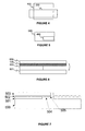
- the layer 101 is a handle wafer of SOI-type.
- the layer 102 is a buried silicon dioxide layer (BOX) and the layer 108 is a top layer in an active layer formed from other wafer comprising the layers 105 and 108, which wafer is bonded on top of the oxidized handle and then thinned 110 down to desired thickness.
- BOX buried silicon dioxide layer
- the thinning is indicated by the mechanical thinning tool 101 as an example in the Figure 1, as being arranged to remove at least a part of the layer 105, which is thus indicated by a dashed line, also for the same reason in Figure 2, in which the layer 105 has been grinded 110 (illustrated in Figure 1), away so making the layer 201 as a residual layer.
- a thin polysilicon layer is embodied as in Figure 2 (layer thickness only illustrative but not in scale).
- the layer 108 is of polysilicon, residing between the active layer 201 in Figure 2 and BOX 102, and this layer 108 getters the impurities from front 201 surface.
- Figure 3 illustrates a method according to an embodiment of the invention for manufacturing a semiconductor wafer structure with an active layer for impurity removal.
- the method comprises phases comprising:
- the etching for a structure that uses a free space somewhere there between the layers of the wafer parts can be made before the bonding.
- a suitable embodiment for instance can be embodied as a switch in very small scale as a micromechanical switch.
- deposition of polysilicon layer was embodied as based on low-pressure CVD, but the technique is not limited only thereto, and thus other techniques of forming polysilicon as such can be used.
- the thermal annealing step can be implemented at least optionally in another way than the bond anneal to reduce or to control the residual stress in the polysilicon layer or to control the chemical composition of the film.
- a polysilicon layer can be used as an anti-stiction layer as formed according to an embodiment of the invention and can be formed by the polysilicon layer, by first annealing it after sacrificial oxide removal to grow grain size and then thermally oxidizing it, and then removing the oxide. In such a way the polysilicon surface can be roughened.
- a layer can be used also as a gettering layer.
- the thermal annealing steps can be at least partly used instead of the bond anneal to reduce or to control the residual stress in the polysilicon layer or control the chemical composition of the film.
- Figure 4 illustrates a component 400 for a mechanical, an electrical and/or electromechanical performance, or a chip 400 for the same, according to an embodiment of the invention.
- the chip is implemented at least partly by a wafer structure 200, from which the by-box-indicated part of the wafer 200 the chip 400 forms.
- the sketching manner is just illustrating, that at least part of the wafer has been used for said component or chip.
- Such a component or chip can be implemented to comprise a circuit of discrete or integrated semiconductor components, optical element, mechanical element and/or a combination of the mentioned.
- Such a chip can comprise a sensor, actuator, transistor, transistor circuit, semi-conductor circuit, FET, MOSFET, diode, detector crystal, sensor, switch, transducer or a combination thereof, for example.
- Figure 5 illustrates a semiconductor device 599 according to an embodiment of the invention that utilizes the chip or a component 400 illustrated in Figure 4.
- FIG 6 it is shown schematically an embodiment of the invention that is related to an anti-stiction application to prevent the layers 603 and 601 to permanently being attached together, by an anti-stiction layer 108 made of polysilicon.
- the layer 602 correspond a layer 102, or can be any layer that is available for separating the layer 601 and the 603 with the polysilicon layer 108 from each other in the specific embodiment.
- Such a polysilicon layer can be made with a rough surface to prevent van der Waals, or other type adhesive forces to cause permanent attachment of layers 603 and 601.
- the polysilicon layer can be doped with a suitable dopant for arranging suitable conductance for the polysilicon in the application.
- the layer 603 can be a part of a micromechanical beam on a substrate in a stack comprising the layers 602 and 108 to form a switch for instance as implemented by a bending structure further implemented by the beam comprising the layers 603 and 108.
- a beam can be planned to be a bending beam for instance as a result of applied electric field therein in the structure. The potential bending is demonstrated by the two-end-arrow-line at the right in the Figure 6.
- the anti-stiction layer comprising polysilicon layer 108 acts also as a gettering layer to getter impurities from the other layers 601, 602, 603.
- the order or number of the layers is not limited by the example, and thus there can be also other layers in the structure, that can be also gettered by the polysilicon layer.
- doping of a layer by a dopant is used to arrange a suitable diffusion coefficient to yield a net transference of an impurity through it into a polysilicon layer used as a gettering layer.
- a wafer comprising an active layer made of at least partly of polysilicon has essentially uniform thickness above 0.1 ⁇ m. According to an embodiment of the invention, a wafer comprising an active layer made of at least partly of polysilicon has essentially uniform thickness above 0,5 ⁇ m. According to an embodiment of the invention, a wafer comprising an active layer made of at least partly of polysilicon has essentially uniform thickness above 1.01 ⁇ m. According to an embodiment of the invention, a wafer comprising an active layer made of at least partly of polysilicon has essentially uniform thickness above 2 ⁇ m. According to an embodiment of the invention, a wafer comprising an active layer made of at least partly of polysilicon has essentially uniform thickness above 5 ⁇ m.
- the wafer comprising polysilicon layer with essentially uniform pre-determined thickness has a layer thickness tolerance of less than 30 %. According to an embodiment of the invention the wafer comprising polysilicon layer with essentially uniform pre-determined thickness has a layer thickness tolerance of less than 10 %. According to an embodiment of the invention the wafer comprising polysilicon layer with essentially uniform pre-determined thickness has a layer thickness tolerance of less than 1 %.
- the layer 501 is a buried oxide layer
- the layer 502 comprises polysilicon layer, which can be formed from an initially amorphous silicon
- the layer 503 is an active layer originating to a thinned silicon layer from second wafer
- layer 504 is a void area where oxide is removed to release active layer and polysilicon layer and the layer 505 is exposed polysilicon layer surface treated in such a way, that stiction of the released area above 504 to the substrate 500 is prevented, although the void distance were in a micron scale layer.
Landscapes
- Thin Film Transistor (AREA)
- Bipolar Transistors (AREA)
- Recrystallisation Techniques (AREA)
- Element Separation (AREA)
Applications Claiming Priority (1)
| Application Number | Priority Date | Filing Date | Title |
|---|---|---|---|
| US11/389,087 US7923353B2 (en) | 2006-03-27 | 2006-03-27 | Gettering method and a wafer using the same |
Publications (2)
| Publication Number | Publication Date |
|---|---|
| EP1840951A2 true EP1840951A2 (fr) | 2007-10-03 |
| EP1840951A3 EP1840951A3 (fr) | 2009-07-08 |
Family
ID=38162308
Family Applications (1)
| Application Number | Title | Priority Date | Filing Date |
|---|---|---|---|
| EP07104846A Withdrawn EP1840951A3 (fr) | 2006-03-27 | 2007-03-26 | Procédé de piégeage et plaquette l'utilisant |
Country Status (8)
| Country | Link |
|---|---|
| US (1) | US7923353B2 (fr) |
| EP (1) | EP1840951A3 (fr) |
| JP (1) | JP2007266607A (fr) |
| KR (1) | KR20070096942A (fr) |
| CN (1) | CN101047128A (fr) |
| CA (1) | CA2582632A1 (fr) |
| SG (2) | SG155984A1 (fr) |
| TW (1) | TW200741824A (fr) |
Families Citing this family (3)
| Publication number | Priority date | Publication date | Assignee | Title |
|---|---|---|---|---|
| KR102225764B1 (ko) * | 2011-01-25 | 2021-03-10 | 에베 그룹 에. 탈너 게엠베하 | 웨이퍼들의 영구적 결합을 위한 방법 |
| US9527721B2 (en) * | 2015-05-15 | 2016-12-27 | Taiwan Semiconductor Manufacturing Co., Ltd. | Movement microelectromechanical systems (MEMS) package |
| US11211259B2 (en) * | 2018-04-20 | 2021-12-28 | Taiwan Semiconductor Manufacturing Company, Ltd. | Structure and method for embedded gettering in a silicon on insulator wafer |
Family Cites Families (11)
| Publication number | Priority date | Publication date | Assignee | Title |
|---|---|---|---|---|
| US5132770A (en) * | 1988-08-25 | 1992-07-21 | Kabushiki Kaisha Toshiba | Semiconductor device having improved multi-layered substrate structure |
| US5417111A (en) * | 1990-08-17 | 1995-05-23 | Analog Devices, Inc. | Monolithic chip containing integrated circuitry and suspended microstructure |
| JPH04127437A (ja) * | 1990-09-18 | 1992-04-28 | Fujitsu Ltd | 半導体基板 |
| JPH04266047A (ja) * | 1991-02-20 | 1992-09-22 | Fujitsu Ltd | 埋め込み層形成に相当するsoi型半導体装置の製造方法及び半導体装置 |
| US5240876A (en) * | 1991-02-22 | 1993-08-31 | Harris Corporation | Method of fabricating SOI wafer with SiGe as an etchback film in a BESOI process |
| US6548382B1 (en) * | 1997-07-18 | 2003-04-15 | Silicon Genesis Corporation | Gettering technique for wafers made using a controlled cleaving process |
| JP3452122B2 (ja) * | 1998-04-22 | 2003-09-29 | 三菱住友シリコン株式会社 | Soi基板の製造方法 |
| JP3452123B2 (ja) * | 1998-04-22 | 2003-09-29 | 三菱住友シリコン株式会社 | Soi基板の製造方法 |
| US6890835B1 (en) * | 2000-10-19 | 2005-05-10 | International Business Machines Corporation | Layer transfer of low defect SiGe using an etch-back process |
| CN1894796B (zh) * | 2003-12-15 | 2010-09-01 | 株式会社半导体能源研究所 | 薄膜集成电路器件的制造方法和非接触薄膜集成电路器件及其制造方法 |
| US7772523B2 (en) * | 2004-07-30 | 2010-08-10 | Semiconductor Energy Laboratory Co., Ltd | Laser irradiation apparatus and laser irradiation method |
-
2006
- 2006-03-27 US US11/389,087 patent/US7923353B2/en active Active
-
2007
- 2007-03-20 TW TW096109425A patent/TW200741824A/zh unknown
- 2007-03-22 SG SG200906418-9A patent/SG155984A1/en unknown
- 2007-03-22 SG SG200702125-6A patent/SG136095A1/en unknown
- 2007-03-26 CA CA002582632A patent/CA2582632A1/fr not_active Abandoned
- 2007-03-26 KR KR1020070029169A patent/KR20070096942A/ko not_active Withdrawn
- 2007-03-26 EP EP07104846A patent/EP1840951A3/fr not_active Withdrawn
- 2007-03-27 CN CNA2007100884765A patent/CN101047128A/zh active Pending
- 2007-03-27 JP JP2007082718A patent/JP2007266607A/ja not_active Withdrawn
Also Published As
| Publication number | Publication date |
|---|---|
| KR20070096942A (ko) | 2007-10-02 |
| EP1840951A3 (fr) | 2009-07-08 |
| JP2007266607A (ja) | 2007-10-11 |
| US7923353B2 (en) | 2011-04-12 |
| US20070224782A1 (en) | 2007-09-27 |
| SG155984A1 (en) | 2009-10-29 |
| TW200741824A (en) | 2007-11-01 |
| CN101047128A (zh) | 2007-10-03 |
| SG136095A1 (en) | 2007-10-29 |
| CA2582632A1 (fr) | 2007-09-27 |
Similar Documents
| Publication | Publication Date | Title |
|---|---|---|
| CN100349278C (zh) | 制备衬底的方法以及使用该方法获得的衬底 | |
| EP1921673B1 (fr) | Procédé de fabrication d'un substrat semi-conducteur | |
| JP2014512091A (ja) | ハンドルウエハ内に高抵抗率領域を有するシリコン・オン・インシュレータ構造体およびそのような構造体の製法 | |
| KR101955375B1 (ko) | 3d 통합 프로세스들로 재료의 층들을 이동시키는 방법들 및 관련 구조들 및 디바이스들 | |
| WO2012003161A1 (fr) | Procédé de conversion assistée par plasma d'oxygène pour préparation d'une surface au collage | |
| CN103247566B (zh) | 绝缘体上硅衬底和形成方法 | |
| US20090001500A1 (en) | Method and structure for implanting bonded substrates for electrical conductivity | |
| US20050124167A1 (en) | Method for forming a cavity and an SOI in a semiconductor substrate, and a semiconductor substrate having a buried cavity and/or an SOI formed therein | |
| EP2012346B1 (fr) | Procédé de fabrication d'une plaquette soi | |
| CN103400797A (zh) | 带有空腔的半导体衬底的制备方法 | |
| US8193595B2 (en) | Method of forming a die having an IC region adjacent a MEMS region | |
| JP5220335B2 (ja) | Soi基板の製造方法 | |
| EP1840951A2 (fr) | Procédé de piégeage et plaquette l'utilisant | |
| US11610808B2 (en) | Semiconductor wafer with low defect count and method for manufacturing thereof | |
| JP2009218381A (ja) | SOI(Silicononinsulator)基板の製造方法 | |
| JP5292810B2 (ja) | Soi基板の製造方法 | |
| JP5096780B2 (ja) | Soiウエーハの製造方法 | |
| CN115513123B (zh) | 一种绝缘体上硅结构及其形成方法 | |
| CN1992173B (zh) | 用于注入键合衬底以便导电的方法和结构 | |
| KR100539465B1 (ko) | 실리콘 박막분리를 위한 표면기포 형성방법 | |
| JP4525892B2 (ja) | Soiウェーハの製造方法 | |
| CN108428664B (zh) | 绝缘体上硅衬底的制造方法 | |
| US20100270658A1 (en) | Semiconductor device and method for producing same | |
| JPH08148659A (ja) | Soi基板の製造方法 | |
| JP2007227459A (ja) | Soi基板の製造方法 |
Legal Events
| Date | Code | Title | Description |
|---|---|---|---|
| PUAI | Public reference made under article 153(3) epc to a published international application that has entered the european phase |
Free format text: ORIGINAL CODE: 0009012 |
|
| AK | Designated contracting states |
Kind code of ref document: A2 Designated state(s): AT BE BG CH CY CZ DE DK EE ES FI FR GB GR HU IE IS IT LI LT LU LV MC MT NL PL PT RO SE SI SK TR |
|
| AX | Request for extension of the european patent |
Extension state: AL BA HR MK YU |
|
| PUAL | Search report despatched |
Free format text: ORIGINAL CODE: 0009013 |
|
| AK | Designated contracting states |
Kind code of ref document: A3 Designated state(s): AT BE BG CH CY CZ DE DK EE ES FI FR GB GR HU IE IS IT LI LT LU LV MC MT NL PL PT RO SE SI SK TR |
|
| AX | Request for extension of the european patent |
Extension state: AL BA HR MK RS |
|
| AKX | Designation fees paid | ||
| REG | Reference to a national code |
Ref country code: DE Ref legal event code: 8566 |
|
| STAA | Information on the status of an ep patent application or granted ep patent |
Free format text: STATUS: THE APPLICATION IS DEEMED TO BE WITHDRAWN |
|
| 18D | Application deemed to be withdrawn |
Effective date: 20100109 |