EP1903354A2 - Vorrichtung zur Messung der Empfangszeit eines Lichtimpulses sowie Abstandsmessung damit - Google Patents
Vorrichtung zur Messung der Empfangszeit eines Lichtimpulses sowie Abstandsmessung damit Download PDFInfo
- Publication number
- EP1903354A2 EP1903354A2 EP07018363A EP07018363A EP1903354A2 EP 1903354 A2 EP1903354 A2 EP 1903354A2 EP 07018363 A EP07018363 A EP 07018363A EP 07018363 A EP07018363 A EP 07018363A EP 1903354 A2 EP1903354 A2 EP 1903354A2
- Authority
- EP
- European Patent Office
- Prior art keywords
- signal
- pulse light
- light receiving
- damping signal
- zero
- Prior art date
- Legal status (The legal status is an assumption and is not a legal conclusion. Google has not performed a legal analysis and makes no representation as to the accuracy of the status listed.)
- Granted
Links
- 238000005259 measurement Methods 0.000 title claims abstract description 66
- 238000013016 damping Methods 0.000 claims abstract description 95
- 230000003287 optical effect Effects 0.000 claims abstract description 33
- 238000001514 detection method Methods 0.000 claims description 3
- 230000003321 amplification Effects 0.000 claims description 2
- 230000002401 inhibitory effect Effects 0.000 claims description 2
- 238000003199 nucleic acid amplification method Methods 0.000 claims description 2
- 230000004044 response Effects 0.000 description 10
- 239000000835 fiber Substances 0.000 description 8
- 238000002310 reflectometry Methods 0.000 description 7
- 230000002238 attenuated effect Effects 0.000 description 6
- 238000010586 diagram Methods 0.000 description 6
- 230000006870 function Effects 0.000 description 4
- 230000003534 oscillatory effect Effects 0.000 description 3
- 230000000630 rising effect Effects 0.000 description 3
- 238000009738 saturating Methods 0.000 description 2
- 230000007423 decrease Effects 0.000 description 1
- 230000006872 improvement Effects 0.000 description 1
- 230000001678 irradiating effect Effects 0.000 description 1
- 238000000034 method Methods 0.000 description 1
- 230000004048 modification Effects 0.000 description 1
- 238000012986 modification Methods 0.000 description 1
- 230000008569 process Effects 0.000 description 1
- 230000009131 signaling function Effects 0.000 description 1
Images




Classifications
-
- G—PHYSICS
- G01—MEASURING; TESTING
- G01S—RADIO DIRECTION-FINDING; RADIO NAVIGATION; DETERMINING DISTANCE OR VELOCITY BY USE OF RADIO WAVES; LOCATING OR PRESENCE-DETECTING BY USE OF THE REFLECTION OR RERADIATION OF RADIO WAVES; ANALOGOUS ARRANGEMENTS USING OTHER WAVES
- G01S17/00—Systems using the reflection or reradiation of electromagnetic waves other than radio waves, e.g. lidar systems
- G01S17/02—Systems using the reflection of electromagnetic waves other than radio waves
- G01S17/06—Systems determining position data of a target
- G01S17/08—Systems determining position data of a target for measuring distance only
- G01S17/10—Systems determining position data of a target for measuring distance only using transmission of interrupted, pulse-modulated waves
-
- G—PHYSICS
- G01—MEASURING; TESTING
- G01S—RADIO DIRECTION-FINDING; RADIO NAVIGATION; DETERMINING DISTANCE OR VELOCITY BY USE OF RADIO WAVES; LOCATING OR PRESENCE-DETECTING BY USE OF THE REFLECTION OR RERADIATION OF RADIO WAVES; ANALOGOUS ARRANGEMENTS USING OTHER WAVES
- G01S7/00—Details of systems according to groups G01S13/00, G01S15/00, G01S17/00
- G01S7/48—Details of systems according to groups G01S13/00, G01S15/00, G01S17/00 of systems according to group G01S17/00
- G01S7/483—Details of pulse systems
- G01S7/486—Receivers
- G01S7/4861—Circuits for detection, sampling, integration or read-out
-
- G—PHYSICS
- G01—MEASURING; TESTING
- G01S—RADIO DIRECTION-FINDING; RADIO NAVIGATION; DETERMINING DISTANCE OR VELOCITY BY USE OF RADIO WAVES; LOCATING OR PRESENCE-DETECTING BY USE OF THE REFLECTION OR RERADIATION OF RADIO WAVES; ANALOGOUS ARRANGEMENTS USING OTHER WAVES
- G01S7/00—Details of systems according to groups G01S13/00, G01S15/00, G01S17/00
- G01S7/48—Details of systems according to groups G01S13/00, G01S15/00, G01S17/00 of systems according to group G01S17/00
- G01S7/483—Details of pulse systems
- G01S7/486—Receivers
- G01S7/487—Extracting wanted echo signals, e.g. pulse detection
-
- G—PHYSICS
- G01—MEASURING; TESTING
- G01S—RADIO DIRECTION-FINDING; RADIO NAVIGATION; DETERMINING DISTANCE OR VELOCITY BY USE OF RADIO WAVES; LOCATING OR PRESENCE-DETECTING BY USE OF THE REFLECTION OR RERADIATION OF RADIO WAVES; ANALOGOUS ARRANGEMENTS USING OTHER WAVES
- G01S7/00—Details of systems according to groups G01S13/00, G01S15/00, G01S17/00
- G01S7/48—Details of systems according to groups G01S13/00, G01S15/00, G01S17/00 of systems according to group G01S17/00
- G01S7/483—Details of pulse systems
- G01S7/486—Receivers
- G01S7/4868—Controlling received signal intensity or exposure of sensor
Definitions
- the present invention relates to improvement and modification in a pulse light receiving time measurement apparatus and a distance measurement apparatus including the pulse light receiving time measurement apparatus.
- a distance measurement apparatus for measuring a distance from the apparatus to a measuring object at a high speed by irradiating pulse light to the object and receiving reflected light from the object at a light receiving element to thereby measure a time from the irradiation of the pulse light to the reflected light's reaching at the light receiving element from the object (See Japanese Patent Application Laid-Open Publication No. 2005-214786 ).
- the conventional metrology device which measures the distance by optically adjusting amount of light cannot deal with the above high-speed measurement of the distance to the object, and moreover, it has to have an optical receiver circuit which can detect amounts of light in a large range from extremely small to large.
- an amplifier used for the optical receiver circuit generally has a dynamic range in which the maximum value is five to ten times as large as the minimum value.
- the dynamic range in which the maximum value is over 1,000 times as large as the minimum value is needed. Therefore, the amplifier needs to be configured to have multiple stages in order to achieve such a large dynamic range.
- An object of the present invention is to provide a pulse light receiving time measurement apparatus suitable for use in a distance measurement apparatus which performs three-dimensional, high-speed measurement of various objects ranging from the natural object with low reflectivity to the retroreflective member with high reflectivity without enlarging the circuit scale, as well as to provide the distance measurement apparatus.
- a pulse light receiving time measurement apparatus includes a light receiving element receiving reflected pulse light from an object to be measured; a pulse light receiving time measurement circuit measuring a time when pulse light is irradiated to the object to be measured and a time when the reflected pulse light from the object to be measured is received at the light receiving element; a resonance circuit converting an optical pulse signal of the reflected pulse light from the light receiving element into a damping signal; a multi-stage amplifier group amplifying the damping signal from the resonance circuit; a damping signal processing circuit composed of amplitude comparators and zero-cross comparators, and processing the damping signal from each stage of the multi-stage amplifier group which is connected with a pair of an amplitude comparator and a zero-cross comparator, the amplitude comparators comparing amplitude of the damping signal with a predetermined value, the zero-cross comparators detecting that the damping signal crosses a bias level; and an integrated logic circuit (13e) combining a plurality of signal lines from the zero-
- the pulse light receiving time measurement apparatus further includes an attenuator composed of a ladder-type resistor, provided between the resonance circuit and the multi-stage amplifier group, and attenuating an amplitude of received pulse light of a large amount at an arbitrary attenuation rate.
- the damping signal from the resonance circuit is input to the attenuator, and a plurality of damping signals voltage-divided arbitrarily by the ladder-type resistor and a damping signal not voltage-divided are input to the multi-stage amplifier group, to expand a range of detection of amounts of light from extremely small to large.
- a pulse light receiving time measurement apparatus includes a light receiving element receiving reflected pulse light from an object to be measured and pulse light guided to an internal optical reference path; a pulse light receiving time measurement circuit measuring a time when pulse light is irradiated to the object to be measured and a time when the reflected pulse light from the object to be measured is received at the light receiving element; a resonance circuit converting an optical pulse signal of each pulse light output from the light receiving element into a damping signal; a multi-stage amplifier group amplifying a damping signal output from the resonance circuit; a damping signal processing circuit composed of amplitude comparators and zero-cross comparators, processing a damping signal output from each of the multi-stage of the amplifier group which is connected with a pair of an amplitude comparator and a zero-cross comparator, and determining operations of the respective zero-cross comparators according to comparison results of the respective amplitude comparators for the amplifier group, the amplitude comparators comparing amplitude of the damping signal with a predetermined value
- the pulse light receiving time measurement apparatus can further include an attenuator composed of a ladder-type resistor, provided between the resonance circuit and the attenuator. It can be configured that the damping signal output from the resonance circuit is input to the attenuator, and a plurality of damping signals voltage-divided by the ladder-type resistor and a damping signal not voltage-divided are input to the multi-stage amplifier group.
- a distance measurement apparatus includes a light receiving element receiving reflected pulse light from an object to be measured and pulse light guided to an internal optical reference path; a resonance circuit converting an optical pulse signal of each pulse light output from the light receiving element into a damping signal; a multi-stage amplifier group amplifying a damping signal output from the resonance circuit; a damping signal processing circuit composed of amplitude comparators and zero-cross comparators, processing a damping signal output from each of the multiple stages of the amplifier group to obtain a signal for acquiring a difference in time between emission of pulse light and the reflected pulse light's reaching the light receiving element; and a processing unit receiving the signal processed by the damping signal processing circuit and obtaining a distance from the measurement apparatus to the object to be measured according to the difference in time acquired.
- the damping signal processing circuit is composed of a group of amplitude comparators comparing amplitude of the damping signal with a predetermined value, and a group of zero-cross comparators detecting that the damping signal crosses a bias level, the amplitude comparators and the zero-cross comparator being of a same number.
- each of the zero-cross comparators outputs the signal for acquiring the difference in time to the processing unit, and each of the amplitude comparators outputs, to each zero-cross comparator, a permit/inhibit signal for selectively permitting/inhibiting the output of the signal for acquiring the difference in time to the processing unit.
- the distance measurement apparatus can further include an attenuator composed of a ladder-type resistor and provided between the resonance circuit and the multi-stage amplifier group.
- the damping signal output from the resonance circuit is input to the attenuator and a plurality of damping signals voltage-divided by the ladder-type resistor and a damping signal not voltage-divided are input to the multi-stage amplifier group.
- the resonance circuit is composed of a plurality of resistors and one or more coils
- the attenuator is composed of one or more transistors and a plurality of resistors.
- the distance measurement apparatus can further include an integrated logic circuit (13e) provided between the damping signal processing circuit and the processing unit and combining respective signal lines from the zero-cross comparators into one for output to the processing unit.
- an integrated logic circuit 13e
- the multi-stage amplifier group is composed of a plurality of amplifiers having a same gain. It can be configured that upon every amplification by each amplifier, the damping signal output from the resonance circuit is amplified by a multiple of a power of the gain.
- Fig. 1 is a block circuit diagram showing an example of the pulse light receiving time measurement apparatus according to the first embodiment of the present invention.
- the number 1 represents the pulse light receiving time measurement apparatus according to the present invention, and OT represents an object to be measured.
- the pulse light receiving time measurement apparatus includes a processing unit 2, a timing signal generator circuit 3, a laser oscillator circuit 4, a light emitting element 5, a half mirror 6, an optical shutter 7, a light guide fiber 8, a triangular prism 9, an objective lens 10, a light guide fiber 11, a half mirror 12, an optical receiver circuit 13, an internal optical reference path 14, an oscillator 15, and an optical shutter 16.
- the processing unit has a function of measuring a distance to an object OT, that is, it mainly function as a pulse light receiving time measurement circuit which measures receipts of optical pulses.
- the timing signal generator circuit 3 supplies a timing signal to the laser oscillator circuit 4 according to a reference signal from the oscillator 15.
- the laser oscillator circuit 4 outputs a driving signal to the light emitting element according to the timing signal.
- the light emitting element 5 is composed of, for example, pulse laser diode, and generates pulse laser light at a predetermined timing.
- the half mirror 6 transmits a part of the pulse laser light from the light emitting element 5 and reflects a part of the rest thereof to the internal optical reference path 14.
- the optical shutter 7 functions to decide whether or not to guide the pulse laser light transmitted through the half mirror 6 to the light guide fiber 8.
- the optical shutter 16 functions to decide whether or not to guide the pulse laser light reflected by the half mirror 6 to the internal optical reference path 14.
- the light guide fiber 8 guides the pulse laser light transmitted through the optical shutter 7 to the triangular prism 9.
- the triangular prism 9 reflects the pulse laser light emitted from the light guide fiber 8 to the objective lens 10.
- the pulse laser light reflected by the triangular prism 9 is irradiated to the object to be measured OT via the objective lens 10.
- the pulse laser light reflected from the object to be measured is converged by the objective lens 10 and guided to the triangular prism 10. Then, it is reflected by the triangular prism 9 to the light guide fiber 11, and transmits through the light guide fiber 11 and is guided to the half mirror 12.
- the pulse laser light guided to the internal optical reference path 14 is guided to the half mirror 12, and then reflected by the half mirror 12 to the light receiving element 13a constituting a part of the optical receiver circuit 13.
- the pulse laser light guided by the light guide fiber 11 transmits through the half mirror 12 to be guided to the light receiving element 13a.
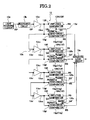
- the optical receiver circuit 13 has, as shown in Fig. 2, a resonance circuit 13b, a multi-stage amplifier group 13c, a damping signal processing part 13d, and an integrated logic circuit 13e.
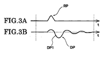
- the light receiving element 13a photoelectrically converts the reflected pulse light into a pulse signal RP shown in Fig. 3A for output.
- the resonance circuit 13b outputs an attenuated oscillatory waveform signal (damping signal) DP in response to the input of the pulse signal RP.
- the attenuated oscillatory waveform signal DP has a waveform in which a mountain like shape and a valley like shape are alternatively, periodically appear, and its amplitude gradually decreases, as shown in Fig. 3B.
- the multi-stage amplifier group 13c is composed of amplifiers 13c1, 13c2, 13c3, and 13c4 with a fixed gain A.
- the gain A is 10
- the damping signal DP output from the resonance circuit 13b is amplified by 10 times by the amplifier 13c1, amplified by 100 times by the amplifier 13c2, amplified by 1,000 times by the amplifier 13c3, and amplified by 10,000 times by the amplifier 13c4.
- the damping signal processing part 13d is composed of an amplitude comparator group 13f and a zero-cross comparator group 13g.
- the amplitude comparator group 13f is composed of amplitude comparators 13f1, 13f2, 13f3, and 13f4.
- the zero-cross comparator group 13g is composed of zero-cross comparators 13g1, 13g2, 13g3, and 13g4.
- the output port 13co of the amplifier 13c1 is connected with the input port 13fi of the amplitude comparator 13fl, the input port 13gi of the zero-cross comparator 13g1, and the input port 13ci of the amplifier 13c2.
- the output port 13co of the amplifier 13c2 is connected with the input port 13fi of the amplitude comparator 13f2, the input port 13gi of the zero-cross comparator 13g2, and the input port 13ci of the amplifier 13c3.
- the output port 13co of the amplifier 13c3 is connected with the input port 13fi of the amplitude comparator 13f3, the input port 13gi of the zero-cross comparator 13g3, and the input port 13ci of the amplifier 13c4.
- the output port 13co of the amplifier 13c4 is connected with the input port 13fi of the amplitude comparator 13f4, and the input port 13gi of the zero-cross comparator 13g4.
- the amplitude comparators 13f1, 13f2, 13f3, and 13f4 as shown in Fig. 4 compares the level of the damping signal DP having a predetermined response waveform DP1 with a reference level R1.
- a reference level R1 When the absolute value of the response waveform DP1 is smaller than the reference level R1, they output an L signal (low-level signal).
- an H signal When the absolute value of the response waveform DP1 is larger than the reference level R1, they output an H signal (high-level signal).
- the H signal functions as a permit signal and an inhibit signal.
- the output port 13fo of the amplitude comparator 13fl is connected with the permit terminal Q1 of the zero-cross comparator 13g1 and the inhibit terminal Q2' of the zero-cross comparator 13g2.
- the output port 13fo of the amplitude comparator 13f2 is connected with the permit terminal Q2 of the zero-cross comparator 13g2 and the inhibit terminal Q3' of the zero-cross comparator 13g3.
- the output port 13fo of the amplitude comparator 13f3 is connected with the permit terminal Q3 of the zero-cross comparator 13g4 and the inhibit terminal Q4' of the zero-cross comparator 13g4.
- the output port 13fo of the amplitude comparator 13f4 is connected with the permit terminal Q4 of the zero-cross comparator 13g4.
- the zero-cross comparators 13g1, 13g2, 13g3, and 13g4 are configured to output the L signal when the L signal is input to the permit terminal thereof, and to output the H signal when the H signal is input to both of the permit and inhibit terminals thereof.
- the zero-cross comparators are configured to output the H signal when the H signal is input to the permit terminal and the L signal is input to the inhibit terminal.
- the absolute value of the response waveform DP1 is smaller than the reference level R1; therefore, the amplitude comparator 13f1 outputs the L signal, and the zero-cross comparator 13g1 outputs the L signal.
- the absolute value of the response waveform DP1 is larger than the reference level R1; therefore, the amplitude comparator 13f2 outputs the H signal, and the zero-cross comparator 13g2 outputs the H signal at a zero-cross point.
- the absolute value of the response waveform DP1 is larger than the reference level R1, so that the zero-cross comparator 13g3 goes into a high level.
- the amplitude comparator 13f2 outputs the H signal
- the zero-cross comparator 13g3 is inhibited from outputting the H signal and remains to output the L signal.
- the amplitude comparator 13f3 outputs the H signal so that the zero-cross comparator 13g4 is inhibited from outputting the H signal and remains to output the L signal.
- the H signal is output from one of the four zero-cross comparators 13g1, 13g2, 13g3, and 13g4, and input to the integrated logic circuit 13e which is composed of an OR circuit, for example. Then, the H signal from the zero-cross comparator is input to a not-shown time-axis measurement circuit which partially constitutes the processing unit 2.
- the processing unit 2 obtains a distance to the object to be measured based on a rising point t0 of the H signal.
- the amplitude comparators 13f1, 13f2, 13f3, and 13f4 and the zero-cross comparator 13g1, 13g2, 13g3, and 13g4 are reset by a reset signal RS.
- the processing unit 2 obtains the distance from the measurement apparatus to the object to be measured OT based on a difference in time between the rising point of the H signal of the zero-cross comparator 13g2, which is obtained from the damping signal based on the pulse laser light guided to the internal optical reference path 14, and the rising point of the H signal obtained from the damping signal corresponding to the reflected pulse light from the object to be measured OT.
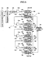
- Fig. 5 shows the optical receiver circuit in the pulse light receiving time measurement apparatus according to the second embodiment of the present invention.
- an attenuator 13h is provided between the resonance circuit 13b and the multi-stage amplifier group 13c.
- the attenuator 13h With the provision of the attenuator 13h, it is made possible to provide uniformly attenuated damping signals DP to the amplifier in the subsequent stage 13c, even when the object to be measured OT is an artificial object within a close distance, and bright reflected pulse light is received at the light receiving element 13a. This accordingly enables the calculation of the light receiving time without saturating the damping signal.
- the second embodiment it is able to process a large amount of received pulse light by attenuating the amplitude of the damping signal at an arbitrary attenuation rate, so that the light receiving time can be calculated without saturating the damping signal, even when bright reflected pulse light is received at the light receiving element 13a.
- Fig. 6 shows the optical receiver circuit in the pulse light receiving time measurement apparatus according to the second embodiment of the present invention.
- a ladder-type attenuator 13i (ladder-type resistor) is provided between the resonance circuitl3b and the multi-stage amplifier group 13c.
- the resonance circuit 13b includes resistors R1, R2, and a coil L1 as shown in Fig. 7.
- the power supply voltage Vcc is applied to one end of the resistor 1 while the other end of the resistor R1 is connected with one end of the resistor R2 and one end of the coil L1.
- the other end of the resistor R2 is grounded (GND), and the other end of the coil L1 is connected with an anode of the light receiving element 13a.
- the power supply voltage Vcc is applied to a cathode of the light receiving element 13a.
- the ladder-type attenuator 13i includes a transistor Tr and resistors R3, R4, and R5.
- a connector of the transistor Tr is applied with the power supply voltage Vcc.
- a base of the transistor Tr is connected with the anode of the light receiving element 13a.
- An emitter of the transistor Tr is connected with one end of the resistor R3 and the input port 13ci of the amplifier 13c3.
- the other end of the resistor 3 is connected with one end of the resistor R4 and the input port 13ci of the amplifier 13c2, while the other end of the resistor 4 is connected with one end of the resistor R5 and the input port 13ci of the amplifier 13c1.
- the other end of the resistor R5 is grounded.
- the resonance circuit 13b Upon receiving the reflected pulse light at the light receiving element 13a, the resonance circuit 13b converts a photoelectrically converted signal thereof into a damping signal DP for input to the base of the transistor Tr.
- the damping signal DP is input to the input port 13ci of the amplifier 13c3 with amplitude coefficient 1.
- the damping signal DP is then attenuated by the amplitude coefficient, for example, 1/10 by the resistor R3, and inputted to the input port 13ci of the amplifier 13c2. Further, the damping signal DP is attenuated by the amplitude coefficient, for example, 1/100 by the resistor R4, and inputted to the input port 13ci of the amplifier 13c1.
- the damping signal DP amplified by 100 is output from the output port 13co of the amplifier 13c4, and the damping signal DP amplified by 10 is output from the output port 13co of the amplifier 13c3.
- the damping signal DP amplified by 1 is output from the output port 13co of the amplifier 13c2, and the damping signal DP amplified 1/10 is output from the output port 13co of the amplifier 13c1.
- the provision of the ladder-type attenuator 13i as described above makes it possible to generate the damping signal with the gain 1 or more from the damping signal with the gain 1 or less. As a result, it is possible to measure, in a wide dynamic range, the distance from the measurement apparatus to various objects which ranges from one with high reflectivity within a close distance or one with low flexibility within a far distance.
- the pulse light receiving time measurement apparatus is configured such that a plurality of damping signals arbitrarily voltage-divided by the ladder-type attenuator 13i and a damping signal not voltage-divided are input to the multi-stage amplifier group 13c, whereby the range of detection of amounts of light can be expanded from extremely small to large.
- the pulse light receiving time measurement apparatus suitable for use in the distance measurement apparatus which performs three-dimensional, high-speed measurement of various objects ranging from the natural object with low reflectivity to the retroreflective member with high reflectivity without enlarging the circuit scale, as well as to provide the distance measurement apparatus.
Landscapes
- Engineering & Computer Science (AREA)
- Physics & Mathematics (AREA)
- Computer Networks & Wireless Communication (AREA)
- General Physics & Mathematics (AREA)
- Radar, Positioning & Navigation (AREA)
- Remote Sensing (AREA)
- Electromagnetism (AREA)
- Optical Radar Systems And Details Thereof (AREA)
- Measurement Of Optical Distance (AREA)
Applications Claiming Priority (1)
| Application Number | Priority Date | Filing Date | Title |
|---|---|---|---|
| JP2006254104A JP5469793B2 (ja) | 2006-09-20 | 2006-09-20 | 距離測定装置 |
Publications (3)
| Publication Number | Publication Date |
|---|---|
| EP1903354A2 true EP1903354A2 (de) | 2008-03-26 |
| EP1903354A3 EP1903354A3 (de) | 2009-06-17 |
| EP1903354B1 EP1903354B1 (de) | 2011-01-26 |
Family
ID=38846958
Family Applications (1)
| Application Number | Title | Priority Date | Filing Date |
|---|---|---|---|
| EP07018363A Not-in-force EP1903354B1 (de) | 2006-09-20 | 2007-09-19 | Vorrichtung zur Messung der Empfangszeit eines Lichtimpulses sowie Abstandsmessung damit |
Country Status (8)
| Country | Link |
|---|---|
| US (1) | US7489390B2 (de) |
| EP (1) | EP1903354B1 (de) |
| JP (1) | JP5469793B2 (de) |
| CN (1) | CN101149431B (de) |
| AT (1) | ATE497180T1 (de) |
| AU (1) | AU2007216862B2 (de) |
| CA (1) | CA2602984C (de) |
| DE (1) | DE602007012182D1 (de) |
Families Citing this family (15)
| Publication number | Priority date | Publication date | Assignee | Title |
|---|---|---|---|---|
| JP4898176B2 (ja) * | 2005-09-26 | 2012-03-14 | 株式会社トプコン | 測量装置及び測量方法 |
| JP5469793B2 (ja) * | 2006-09-20 | 2014-04-16 | 株式会社トプコン | 距離測定装置 |
| US8352128B2 (en) * | 2009-09-25 | 2013-01-08 | TMEIC Corp. | Dynamic protective envelope for crane suspended loads |
| JP2014102072A (ja) * | 2011-03-08 | 2014-06-05 | National Univ Corp Shizuoka Univ | 距離測定用の信号処理回路および距離測定装置 |
| CN102636151A (zh) * | 2012-04-19 | 2012-08-15 | 王振兴 | 激光测距仪及其测距方法 |
| DE102013100696B3 (de) * | 2013-01-24 | 2013-11-07 | Sick Ag | Optoelektronischer Sensor und Verfahren zur Erfassung von Objekten in einem Überwachungsbereich |
| DE102014102209A1 (de) * | 2014-02-20 | 2015-08-20 | Sick Ag | Entfernungsmessender Sensor und Verfahren zur Abstandsbestimmung von Objekten in einem Ueberwachungsbereich |
| CN104777470A (zh) * | 2015-03-20 | 2015-07-15 | 中国科学院合肥物质科学研究院 | 一种扩展脉冲激光近程动态增益范围电路 |
| JP7076947B2 (ja) * | 2017-03-31 | 2022-05-30 | 株式会社トプコン | 測量装置、測量方法及び測量装置の制御プログラム |
| JP6696624B2 (ja) * | 2017-05-24 | 2020-05-20 | 三菱電機ビルテクノサービス株式会社 | 形状測定装置 |
| US10830880B2 (en) * | 2018-03-20 | 2020-11-10 | Panosense Inc. | Selecting LIDAR pulse detector depending on pulse type |
| US10759635B2 (en) | 2018-06-05 | 2020-09-01 | Abraham Ben Seutter | SIDAS—spreader impact damage avoidance system |
| CN109143251B (zh) * | 2018-07-30 | 2023-04-25 | 南京理工大学 | 基于差分信号的脉冲激光测距时刻鉴别器 |
| CN109212544B (zh) * | 2018-09-11 | 2021-06-22 | 深圳市前海腾际创新科技有限公司 | 一种目标距离探测方法、装置及系统 |
| US11422268B1 (en) * | 2018-09-27 | 2022-08-23 | United States Of America As Represented By The Administrator Of Nasa | Long distance space flight laser range finder |
Family Cites Families (15)
| Publication number | Priority date | Publication date | Assignee | Title |
|---|---|---|---|---|
| GB2034140A (en) * | 1978-08-30 | 1980-05-29 | Secr Defence | Analog/digital conversion |
| DE3103567A1 (de) * | 1981-02-03 | 1982-08-12 | MITEC Moderne Industrietechnik GmbH, 8012 Ottobrunn | Entfernungsmessverfahren nach dem prinzip der laufzeitmessung eines messlichtimpulses und vorrichtung zu seiner durchfuehrung |
| JPH01169381A (ja) * | 1987-12-25 | 1989-07-04 | Omron Tateisi Electron Co | 距離測定装置 |
| JP3175489B2 (ja) * | 1994-08-24 | 2001-06-11 | 三菱電機株式会社 | 振動ジャイロおよび振動ジャイロの検査装置 |
| JP3899577B2 (ja) * | 1996-02-28 | 2007-03-28 | マツダ株式会社 | 距離測定装置 |
| JPH11142519A (ja) * | 1997-11-06 | 1999-05-28 | Omron Corp | 光学式距離測定装置 |
| JPH11325823A (ja) * | 1998-05-14 | 1999-11-26 | Omron Corp | 距離計測装置およびこれを用いた物体検出装置ならびに受光信号処理回路 |
| JP2002311138A (ja) * | 2001-04-06 | 2002-10-23 | Mitsubishi Electric Corp | 車両用測距装置 |
| JP3835219B2 (ja) * | 2001-08-31 | 2006-10-18 | オムロン株式会社 | 距離測定装置 |
| JP3911575B2 (ja) * | 2001-12-18 | 2007-05-09 | 株式会社トプコン | パルス方式の光波距離計 |
| JP4832720B2 (ja) | 2004-01-29 | 2011-12-07 | 株式会社トプコン | パルス信号の処理装置、パルス信号の処理方法およびプログラム |
| JP2006105688A (ja) * | 2004-10-01 | 2006-04-20 | Denso Corp | 車両用レーダ装置 |
| JP4898176B2 (ja) * | 2005-09-26 | 2012-03-14 | 株式会社トプコン | 測量装置及び測量方法 |
| US7405812B1 (en) * | 2006-05-18 | 2008-07-29 | Canesta, Inc. | Method and system to avoid inter-system interference for phase-based time-of-flight systems |
| JP5469793B2 (ja) * | 2006-09-20 | 2014-04-16 | 株式会社トプコン | 距離測定装置 |
-
2006
- 2006-09-20 JP JP2006254104A patent/JP5469793B2/ja not_active Expired - Fee Related
-
2007
- 2007-09-19 EP EP07018363A patent/EP1903354B1/de not_active Not-in-force
- 2007-09-19 AT AT07018363T patent/ATE497180T1/de active
- 2007-09-19 DE DE602007012182T patent/DE602007012182D1/de active Active
- 2007-09-19 US US11/901,829 patent/US7489390B2/en active Active
- 2007-09-19 CA CA2602984A patent/CA2602984C/en not_active Expired - Fee Related
- 2007-09-19 CN CN200710154168.8A patent/CN101149431B/zh not_active Expired - Fee Related
- 2007-09-20 AU AU2007216862A patent/AU2007216862B2/en not_active Ceased
Non-Patent Citations (1)
| Title |
|---|
| None |
Also Published As
| Publication number | Publication date |
|---|---|
| CN101149431A (zh) | 2008-03-26 |
| CN101149431B (zh) | 2010-12-08 |
| AU2007216862B2 (en) | 2012-09-27 |
| EP1903354A3 (de) | 2009-06-17 |
| JP5469793B2 (ja) | 2014-04-16 |
| JP2008076145A (ja) | 2008-04-03 |
| EP1903354B1 (de) | 2011-01-26 |
| US7489390B2 (en) | 2009-02-10 |
| DE602007012182D1 (de) | 2011-03-10 |
| US20080068585A1 (en) | 2008-03-20 |
| ATE497180T1 (de) | 2011-02-15 |
| CA2602984C (en) | 2012-06-05 |
| AU2007216862A1 (en) | 2008-04-03 |
| CA2602984A1 (en) | 2008-03-20 |
Similar Documents
| Publication | Publication Date | Title |
|---|---|---|
| EP1903354B1 (de) | Vorrichtung zur Messung der Empfangszeit eines Lichtimpulses sowie Abstandsmessung damit | |
| JP4694304B2 (ja) | 測量装置 | |
| US7212278B2 (en) | Method and device for recording a three-dimensional distance-measuring image | |
| TWI333541B (en) | Laser range finder and related range measurement method | |
| JP4901128B2 (ja) | 距離測定装置、及び距離測定方法 | |
| US8755037B2 (en) | Distance measuring device | |
| US6288775B1 (en) | Lightwave distance measuring apparatus and method | |
| JPH1123709A (ja) | 距離測定装置 | |
| JP5218513B2 (ja) | 変位センサ | |
| CN107817484B (zh) | 激光雷达放大电路的放大倍数处理方法及装置 | |
| US4181431A (en) | Laser distance measuring apparatus | |
| CN116034250B (zh) | 光电传感器以及光测距装置 | |
| US6587185B1 (en) | Distance measuring apparatus | |
| CN108027426B (zh) | 具有改善的动态范围的大地测量仪 | |
| US20030035097A1 (en) | Method and apparatus for locating object by using laser range finder | |
| US5013907A (en) | Optical time domain testing instrument | |
| JP5432885B2 (ja) | Apdの自動調整機能を備えた光パルス試験器またはその方法 | |
| US7599045B2 (en) | Method for eliminating internal reflection of range finding system and range finding system applying the same | |
| JP5515199B2 (ja) | 光パルス試験装置及びその調整方法 | |
| JPH01257289A (ja) | レーザ測距装置 | |
| JPH02309220A (ja) | 光ファイバ式分布形温度計測装置 | |
| JP2003270346A (ja) | パルス信号生成回路および距離測定装置 | |
| JPS62204138A (ja) | 光フアイバ測定器 | |
| US20060181694A1 (en) | Method for eliminating internal reflection of range finding system and range finding system applying the same | |
| KR20220114897A (ko) | 자기 센서 |
Legal Events
| Date | Code | Title | Description |
|---|---|---|---|
| PUAI | Public reference made under article 153(3) epc to a published international application that has entered the european phase |
Free format text: ORIGINAL CODE: 0009012 |
|
| 17P | Request for examination filed |
Effective date: 20070919 |
|
| AK | Designated contracting states |
Kind code of ref document: A2 Designated state(s): AT BE BG CH CY CZ DE DK EE ES FI FR GB GR HU IE IS IT LI LT LU LV MC MT NL PL PT RO SE SI SK TR |
|
| AX | Request for extension of the european patent |
Extension state: AL BA HR MK YU |
|
| PUAL | Search report despatched |
Free format text: ORIGINAL CODE: 0009013 |
|
| AK | Designated contracting states |
Kind code of ref document: A3 Designated state(s): AT BE BG CH CY CZ DE DK EE ES FI FR GB GR HU IE IS IT LI LT LU LV MC MT NL PL PT RO SE SI SK TR |
|
| AX | Request for extension of the european patent |
Extension state: AL BA HR MK RS |
|
| 17Q | First examination report despatched |
Effective date: 20100104 |
|
| AKX | Designation fees paid |
Designated state(s): AT CH DE FR LI |
|
| GRAP | Despatch of communication of intention to grant a patent |
Free format text: ORIGINAL CODE: EPIDOSNIGR1 |
|
| GRAS | Grant fee paid |
Free format text: ORIGINAL CODE: EPIDOSNIGR3 |
|
| GRAA | (expected) grant |
Free format text: ORIGINAL CODE: 0009210 |
|
| AK | Designated contracting states |
Kind code of ref document: B1 Designated state(s): AT CH DE FR LI |
|
| REG | Reference to a national code |
Ref country code: CH Ref legal event code: EP |
|
| REF | Corresponds to: |
Ref document number: 602007012182 Country of ref document: DE Date of ref document: 20110310 Kind code of ref document: P |
|
| REG | Reference to a national code |
Ref country code: DE Ref legal event code: R096 Ref document number: 602007012182 Country of ref document: DE Effective date: 20110310 |
|
| REG | Reference to a national code |
Ref country code: CH Ref legal event code: NV Representative=s name: BRAUNPAT BRAUN EDER AG |
|
| PLBE | No opposition filed within time limit |
Free format text: ORIGINAL CODE: 0009261 |
|
| STAA | Information on the status of an ep patent application or granted ep patent |
Free format text: STATUS: NO OPPOSITION FILED WITHIN TIME LIMIT |
|
| 26N | No opposition filed |
Effective date: 20111027 |
|
| REG | Reference to a national code |
Ref country code: DE Ref legal event code: R097 Ref document number: 602007012182 Country of ref document: DE Effective date: 20111027 |
|
| REG | Reference to a national code |
Ref country code: FR Ref legal event code: PLFP Year of fee payment: 9 |
|
| PGFP | Annual fee paid to national office [announced via postgrant information from national office to epo] |
Ref country code: AT Payment date: 20150825 Year of fee payment: 9 Ref country code: FR Payment date: 20150811 Year of fee payment: 9 |
|
| REG | Reference to a national code |
Ref country code: AT Ref legal event code: MM01 Ref document number: 497180 Country of ref document: AT Kind code of ref document: T Effective date: 20160919 |
|
| REG | Reference to a national code |
Ref country code: FR Ref legal event code: ST Effective date: 20170531 |
|
| PG25 | Lapsed in a contracting state [announced via postgrant information from national office to epo] |
Ref country code: FR Free format text: LAPSE BECAUSE OF NON-PAYMENT OF DUE FEES Effective date: 20160930 |
|
| PG25 | Lapsed in a contracting state [announced via postgrant information from national office to epo] |
Ref country code: AT Free format text: LAPSE BECAUSE OF NON-PAYMENT OF DUE FEES Effective date: 20160919 |
|
| PGFP | Annual fee paid to national office [announced via postgrant information from national office to epo] |
Ref country code: DE Payment date: 20170912 Year of fee payment: 11 Ref country code: CH Payment date: 20170912 Year of fee payment: 11 |
|
| REG | Reference to a national code |
Ref country code: CH Ref legal event code: PCAR Free format text: NEW ADDRESS: HOLEESTRASSE 87, 4054 BASEL (CH) |
|
| REG | Reference to a national code |
Ref country code: DE Ref legal event code: R119 Ref document number: 602007012182 Country of ref document: DE |
|
| REG | Reference to a national code |
Ref country code: CH Ref legal event code: PL |
|
| PG25 | Lapsed in a contracting state [announced via postgrant information from national office to epo] |
Ref country code: DE Free format text: LAPSE BECAUSE OF NON-PAYMENT OF DUE FEES Effective date: 20190402 |
|
| PG25 | Lapsed in a contracting state [announced via postgrant information from national office to epo] |
Ref country code: CH Free format text: LAPSE BECAUSE OF NON-PAYMENT OF DUE FEES Effective date: 20180930 Ref country code: LI Free format text: LAPSE BECAUSE OF NON-PAYMENT OF DUE FEES Effective date: 20180930 |