EP1928087B1 - Circuit amplificateur à gain variable - Google Patents
Circuit amplificateur à gain variable Download PDFInfo
- Publication number
- EP1928087B1 EP1928087B1 EP07020764A EP07020764A EP1928087B1 EP 1928087 B1 EP1928087 B1 EP 1928087B1 EP 07020764 A EP07020764 A EP 07020764A EP 07020764 A EP07020764 A EP 07020764A EP 1928087 B1 EP1928087 B1 EP 1928087B1
- Authority
- EP
- European Patent Office
- Prior art keywords
- circuit
- transistor
- terminal
- signal
- voltage
- Prior art date
- Legal status (The legal status is an assumption and is not a legal conclusion. Google has not performed a legal analysis and makes no representation as to the accuracy of the status listed.)
- Not-in-force
Links
Images

Classifications
-
- H—ELECTRICITY
- H03—ELECTRONIC CIRCUITRY
- H03F—AMPLIFIERS
- H03F3/00—Amplifiers with only discharge tubes or only semiconductor devices as amplifying elements
- H03F3/45—Differential amplifiers
-
- H—ELECTRICITY
- H03—ELECTRONIC CIRCUITRY
- H03G—CONTROL OF AMPLIFICATION
- H03G1/00—Details of arrangements for controlling amplification
- H03G1/0005—Circuits characterised by the type of controlling devices operated by a controlling current or voltage signal
- H03G1/0017—Circuits characterised by the type of controlling devices operated by a controlling current or voltage signal the device being at least one of the amplifying solid-state elements
- H03G1/0023—Circuits characterised by the type of controlling devices operated by a controlling current or voltage signal the device being at least one of the amplifying solid-state elements in emitter-coupled or cascode amplifiers
-
- H—ELECTRICITY
- H03—ELECTRONIC CIRCUITRY
- H03F—AMPLIFIERS
- H03F3/00—Amplifiers with only discharge tubes or only semiconductor devices as amplifying elements
- H03F3/45—Differential amplifiers
- H03F3/45071—Differential amplifiers with semiconductor devices only
- H03F3/45076—Differential amplifiers with semiconductor devices only characterised by the way of implementation of the active amplifying circuit in the differential amplifier
- H03F3/4508—Differential amplifiers with semiconductor devices only characterised by the way of implementation of the active amplifying circuit in the differential amplifier using bipolar transistors as the active amplifying circuit
- H03F3/45085—Long tailed pairs
-
- H—ELECTRICITY
- H03—ELECTRONIC CIRCUITRY
- H03F—AMPLIFIERS
- H03F3/00—Amplifiers with only discharge tubes or only semiconductor devices as amplifying elements
- H03F3/45—Differential amplifiers
- H03F3/45071—Differential amplifiers with semiconductor devices only
- H03F3/45076—Differential amplifiers with semiconductor devices only characterised by the way of implementation of the active amplifying circuit in the differential amplifier
- H03F3/45475—Differential amplifiers with semiconductor devices only characterised by the way of implementation of the active amplifying circuit in the differential amplifier using IC blocks as the active amplifying circuit
-
- H—ELECTRICITY
- H03—ELECTRONIC CIRCUITRY
- H03F—AMPLIFIERS
- H03F3/00—Amplifiers with only discharge tubes or only semiconductor devices as amplifying elements
- H03F3/72—Gated amplifiers, i.e. amplifiers which are rendered operative or inoperative by means of a control signal
-
- H—ELECTRICITY
- H03—ELECTRONIC CIRCUITRY
- H03G—CONTROL OF AMPLIFICATION
- H03G1/00—Details of arrangements for controlling amplification
- H03G1/0005—Circuits characterised by the type of controlling devices operated by a controlling current or voltage signal
- H03G1/0088—Circuits characterised by the type of controlling devices operated by a controlling current or voltage signal using discontinuously variable devices, e.g. switch-operated
-
- H—ELECTRICITY
- H03—ELECTRONIC CIRCUITRY
- H03G—CONTROL OF AMPLIFICATION
- H03G3/00—Gain control in amplifiers or frequency changers
- H03G3/20—Automatic control
-
- H—ELECTRICITY
- H03—ELECTRONIC CIRCUITRY
- H03F—AMPLIFIERS
- H03F2203/00—Indexing scheme relating to amplifiers with only discharge tubes or only semiconductor devices as amplifying elements covered by H03F3/00
- H03F2203/45—Indexing scheme relating to differential amplifiers
- H03F2203/45138—Two or more differential amplifiers in IC-block form are combined, e.g. measuring amplifiers
-
- H—ELECTRICITY
- H03—ELECTRONIC CIRCUITRY
- H03F—AMPLIFIERS
- H03F2203/00—Indexing scheme relating to amplifiers with only discharge tubes or only semiconductor devices as amplifying elements covered by H03F3/00
- H03F2203/45—Indexing scheme relating to differential amplifiers
- H03F2203/45506—Indexing scheme relating to differential amplifiers the CSC comprising only one switch
-
- H—ELECTRICITY
- H03—ELECTRONIC CIRCUITRY
- H03F—AMPLIFIERS
- H03F2203/00—Indexing scheme relating to amplifiers with only discharge tubes or only semiconductor devices as amplifying elements covered by H03F3/00
- H03F2203/45—Indexing scheme relating to differential amplifiers
- H03F2203/45528—Indexing scheme relating to differential amplifiers the FBC comprising one or more passive resistors and being coupled between the LC and the IC
-
- H—ELECTRICITY
- H03—ELECTRONIC CIRCUITRY
- H03F—AMPLIFIERS
- H03F2203/00—Indexing scheme relating to amplifiers with only discharge tubes or only semiconductor devices as amplifying elements covered by H03F3/00
- H03F2203/45—Indexing scheme relating to differential amplifiers
- H03F2203/45652—Indexing scheme relating to differential amplifiers the LC comprising one or more further dif amp stages, either identical to the dif amp or not, in cascade
-
- H—ELECTRICITY
- H03—ELECTRONIC CIRCUITRY
- H03F—AMPLIFIERS
- H03F2203/00—Indexing scheme relating to amplifiers with only discharge tubes or only semiconductor devices as amplifying elements covered by H03F3/00
- H03F2203/72—Indexing scheme relating to gated amplifiers, i.e. amplifiers which are rendered operative or inoperative by means of a control signal
- H03F2203/7231—Indexing scheme relating to gated amplifiers, i.e. amplifiers which are rendered operative or inoperative by means of a control signal the gated amplifier being switched on or off by putting into cascade or not, by choosing between amplifiers by one or more switch(es)
Definitions
- the present invention generally relates to variable gain amplifier circuits, and particularly to variable gain amplifier circuits adjusting the level of audio signal by varying the gain of the signal based on a control signal.
- variable gain amplifier circuit As an exemplary variable gain amplifier circuit, there is known a variable gain amplifier circuit adjusting the level of an audio signal by varying the gain of the signal based on a control signal corresponding to the peak-to-peak level of the audio signal captured from various audio sources.
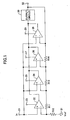
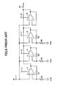
- FIG. 6 is a schematic circuit diagram of a conventional variable gain amplifier circuit integrated into a semiconductor chip. As shown in FIG. 6 , an audio signal from various audio sources is input into a terminal 1, and the input audio signal is supplied to each non-inverting input terminal of operational amplifiers 2, 4, 6, 8.
- the output terminal and the inverting input terminal of the operational amplifier 2 are connected to each other via a resistor R1.
- the inverting input terminal is connected to one end of resistor R2.
- a referential voltage (Vref) is applied to the other end of the resistor R2.
- the output terminal of the operational amplifier 2 is connected to a terminal 10.
- the operational amplifier 2 is configured as a non-inverting amplifier.
- the operational amplifier 2 operates only when, for example, a high-level control signal is supplied to the terminal 3 of the operational amplifier 2.
- the output terminal and the inverting input terminal of the operational amplifier 4 are connected to each other via a resistor R3.
- the inverting input terminal is connected to one end of resistor R4.
- the referential voltage (Vref) is applied to the other end of the resistor R4.
- the output terminal of the operational amplifier 4 is connected to a terminal 10.
- the operational amplifier 4 is configured as a non-inverting amplifier.
- the operational amplifier 4 operates only when, for example, a high-level control signal is supplied to the terminal 5 of the operational amplifier 4.
- the output terminal and the inverting input terminal of the operational amplifier 6 are connected to each other via a resistor R5.
- the inverting input terminal is connected to one end of resistor R6.
- the referential voltage (Vref) is applied to the other end of the resistor R6.
- the output terminal of the operational amplifier 4 is connected to a terminal 10.
- the operational amplifier 6 is configured as a non-inverting amplifier.
- the operational amplifier 6 operates only when, for example, a high-level control signal is supplied to the terminal 7 of the operational amplifier 6.
- the output terminal and the inverting input terminal of the operational amplifier 8 are connected to each other.
- the output terminal of the operational amplifier 8 is connected to the terminal 10.
- the operational amplifier 8 is configured as a buffer amplifier.
- the operational amplifier 8 operates only when, for example, a high-level control signal is supplied to the terminal 9 of the operational amplifier 8.
- the amplification of the buffer amplifier is 0 dB (1 time).
- Only one of the control signals supplied to the terminals 3, 5, 7, 9 is high-level. Accordingly, only one of the operational amplifiers 2, 4, 6, 8 is to be operated and an audio signal amplified by the one of the operational amplifiers 2, 4, 6, 8 is output from the terminal 10.
- FIG. 7 is a schematic circuit diagram of an exemplary non-inverting amplifier of the operational amplifier 2.
- the configuration of the other non-inverting amplifiers of the operational amplifiers 4, 6, 8 is substantially the same as the configuration of the operational amplifier 2.
- the emitters of npn transistors Q1, Q2 are connected to each other and are grounded via a constant current source 11 and a switch 12.
- the base of the transistor Q1 is connected to a terminal 1, and the collector of the transistor Q1 is connected to voltage Vcc via a constant current source 13.
- the base of the transistor Q2 is connected to the junction of one end of resistor R1 and one end of resistor R2.
- the collector of the transistor Q2 is connected to the voltage Vcc.
- a differential circuit is configured with the transistors Q1 and Q2.
- the collector of the transistor Q1 that is the output of the differential circuit, is connected to the base of a pnp transistor Q3.
- the emitter of the transistor Q3 is connected to the voltage Vcc.
- the collector of the transistor Q3 is grounded via a constant current source 14 and a switch 15. As a result, the transistor Q3 operates as an output circuit with the emitter grounded.
- the collector of the transistor Q3 is connected to the terminal 10, the base of the transistor Q2 via the resistor R1, and the base of the transistor Q3 via a capacitor C0 for phase compensation.
- the reference voltage is applied to the base of the transistor Q2 via the resistor R2.
- Switches 12, 15 are closed only when high-level control signal is applied to the terminal 3 to flow current through transistors Q1 through Q3.
- Japanese Utility Model Publication Application No. H4-102311 discloses an amplifier circuit in which gain of the amplifier circuit is determined by selecting only one of two differential amplifier circuits in the amplifier circuit so as to apply power to the selected differential amplifier only.
- FIG. 6 is a schematic circuit diagram showing an example of a conventional variable gain amplifier circuit.
- the resistors R1 through R6 are necessary to be provided to set the amplification of each non-inverting amplifier.
- an output circuit including a transistor, a constant-current source, and a switch is necessary for each non-inverting amplifier.
- the number of circuit elements of the above conventional variable gain amplifier circuit is large and, accordingly, the area of semiconductor integrated circuits becomes large to integrate the circuit elements in the semiconductor integrated circuit.
- US 2005/057304 A1 describes an amplifier with an input terminal to receive an input signal.
- the output stage provides inverting and non-inverting differential output signals on inverting and non-inverting output nodes. However, it does not include a number of resistors connected in series between the signal output terminal and a terminal to which a reference voltage is applied in accordance with the present invention.
- the present invention was made in light of the above-mentioned disadvantages, and may provide a variable gain amplifier circuit having relatively fewer circuit elements and thereby reducing the area required to form the circuit in a semiconductor integrated circuit.
- a variable gain amplifier circuit includes: plural differential circuits (22, 24, 26, 28), each having two input terminals and one output terminal, one of the input terminals of each of the differential circuits being connected in common to a signal input terminal to input a signal to each of the differential circuits, any one of the differential circuits (22, 24, 26, 28) being selected to operate; an output circuit (30) having an input terminal connected in common to each output terminal of the differential circuits (22, 24, 26, 28) and one signal output terminal (50), the output circuit inputting an output signal of any of differential circuits (22, 24, 26, 28) and outputting an output signal from the signal output terminal (50); and plural resistors (R12, R11, R13, R14) connected in series between the signal output terminal (50) of the output circuit (30) and a terminal (51) to which a reference voltage is applied, in which each of junctions between the resistors (R12, R11, R13, R14) is connected to one of the other input
- each of the differential circuits (22, 24, 26, 28) includes a pair of transistors; and a collector of a transistor whose base is regarded as the one of the input terminals of the differential circuits is connected to the output terminal.
- variable gain amplifier circuit in which the output circuit (30) includes a common-emitter transistor whose base is connected to each of the output terminal of the differential circuits and whose collector is connected to the signal output terminal (50).
- the number of resistors used for setting amplification of each non-inverting amplifier may be reduced, thereby reducing the area required to form a variable gain amplifier circuit in a semiconductor integrated circuit.
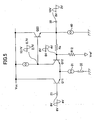
- FIG. 1 is a schematic circuit diagram showing an exemplary variable gain amplifier circuit according to an embodiment of the present invention.
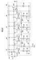
- FIG. 2 is a circuit diagram showing an exemplary variable gain amplifier circuit according to an embodiment of the present invention. It should be noted that the entire variable gain amplifier circuit is formed in a semiconductor integrated circuit.
- an audio signal from various audio sources is input into a signal input terminal 21.
- the input audio signal is supplied in common to each non-inverting input terminal of differential circuits 22, 24, 26, 28.
- the output terminal of the differential circuit 22 is connected to a signal output terminal 50 via an output circuit 30.
- the inverting input terminal of the differential circuit 22 is connected to the junction of one end of resistor R11 and one end of resistor R12.
- the other end of the resistor R12 is connected to a terminal 51 where a reference voltage Vref is applied.
- the other end of the resistor R11 is connected to the signal output terminal 50 via resistors R13, R14.
- Control signals are separately supplied to terminals 23, 25, 27, and 29. Only one of the control signals is high-level. When the high-level control signal is supplied to the terminal 23 of the differential circuit 22, only the differential circuit 22 operates.
- the output terminal of the differential circuit 24 is connected to the signal output terminal 50 via the output circuit 30.
- the inverting input terminal of the differential circuit 24 is connected to the junction of one end of resistor R11 and one end of resistor R13.
- the other end of the resistor R11 is connected to the terminal 51 via the resistor R12.
- the other end of the resistor R13 is connected to the signal output terminal 50 via resistor R14.
- the output terminal of the differential circuit 26 is connected to the signal output terminal 50 via the output circuit 30.
- the inverting input terminal of the differential circuit 26 is connected to the junction of one end of resistor R13 and one end of resistor R14.
- the other end of the resistor R13 is connected to the terminal 51 via the resistors R11 and R12.
- the other end of the resistor R14 is connected to the signal output terminal 50.
- the output terminal of the differential circuit 28 is connected to the signal output terminal 50 via the output circuit 30.
- the inverting input terminal of the differential circuit 28 is connected to the junction of one end of resistor R14 and the signal output terminal 50.
- the emitters of npn transistors Q11, Q12 are commonly grounded via a constant current source 31 and a switch 32.
- the base of the transistor Q11 is connected to an input terminal 21.
- the collector of the transistor Q11 is connected to voltage Vcc via a constant current source 33.
- the base of the transistor Q12 is connected to the junction of one end of resistor R11 and one end of resistor R12.
- the collector of the transistor Q12 is connected to the voltage Vcc.
- the transistors Q11, Q12 constitute the differential circuit 22.
- npn transistors Q13, Q14 are commonly grounded via a constant current source 34 and a switch 35.
- the base of the transistor Q13 is connected to an input terminal 21.
- the collector of the transistor Q13 is connected to voltage Vcc via a constant current source 33.
- the base of the transistor Q14 is connected to the junction of one end of resistor R11 and one end of resistor R13.
- the collector of the transistor Q14 is connected to the voltage Vcc.
- npn transistors Q15, Q16 are commonly grounded via a constant current source 36 and a switch 37.
- the base of the transistor Q15 is connected to an input terminal 21.
- the collector of the transistor Q15 is connected to voltage Vcc via a constant current source 33.
- the base of the transistor Q16 is connected to the junction of one end of resistor R13 and one end of resistor R14.
- the collector of the transistor Q16 is connected to the voltage Vcc.
- npn transistors Q17, Q18 are commonly grounded via a constant current source 38 and a switch 39.
- the base of the transistor Q17 is connected to an input terminal 21.
- the collector of the transistor Q17 is connected to voltage Vcc via a constant current source 33.
- the base of the transistor Q18 is connected to the junction of one end of resistor R14 and the signal output terminal 50.
- the collector of the transistor Q18 is connected to the voltage Vcc.
- the collectors of the transistors Q11, Q13, Q15, and Q17, which are outputs of the differential circuits 22, 24, 26, and 28, respectively, are connected in common to the base of npn transistor Q19 of the output circuit 30.
- the emitter of the transistor Q19 is connected to the voltage Vcc.
- the collector of the transistor Q19 is grounded via a constant current source 40.
- the transistor Q19 forms a common-emitter circuit.
- the collector of the transistor Q19 is connected to the signal output terminal 50, and the base of the transistor Q19 via a capacitor C1 for phase compensation.
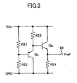
- FIG. 3 is a circuit diagram showing a reference voltage generating circuit connected to the terminal 51 according to an embodiment of the present invention.
- resistors R21 and R22 are connected in series between voltage Vcc and circuit ground. Because of the configuration, the voltage at the junction between the resistor R21 and R22 is given by the formula: Vcc*(R22/(R21+R22)).
- the voltage is output from a terminal 60 as a reference voltage Vref via an emitter follower circuit including a transistor Qa and a resistor R23 and another emitter follower circuit including a transistor Qb and a resistor R24.
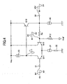
- FIG. 4 is a circuit diagram extracting the differential circuit 22 and the output circuit 30 from the circuit diagram of FIG. 2 .
- FIG. 5 is a circuit diagram modified from the circuit diagram of FIG. 4 .
- the inverted signal from the collector of the transistor Q11 is further inverted by the common-emitter transistor Q19, and the further inverted signal is output from the signal output terminal 50.
- a signal having the same phase as that of the input signal from the terminal 21 is transmitted to the base of an npn transistor Q20 forming an emitter follower circuit, and the signal is output from the signal output terminal 50.
- the base voltage of the transistor Q12 which is a divided voltage of the voltage at the signal output terminal 50, is given by the resistances of the resistors Ra and R12. Therefore, the base voltage of the transistor Q12 changes between a minimum voltage 4 V and a maximum voltage 8 V with a center voltage of 6 V. In this case, however, the minimum voltage of the base of the transistor Q12 is 4 V, and the minimum voltage of the collector of the transistor Q12 is 2.7 V. Therefore, the bias voltage applied between the base and the collector of the transistor 12 is so low that the transistor cannot work normally because an input signal close to the minimum voltage level becomes OFF.
- the voltage at the signal output terminal 50 changes between a minimum voltage 2 V and a maximum voltage 10 V with a center voltage of 6 V.
- the base voltage of the transistor Q12 is a divided voltage of the voltage at the signal output terminal 50 and can be given by the resistances of the resistors Ra and R12, the base voltage of the transistor Q12 changes between a minimum voltage 4 V and a maximum voltage 8 V with a center voltage of 6 V.
- the voltage of the collector of the transistor 12 is the voltage Vcc, the transistor Q12 can operate in the full range between the minimum and the maximum values of the signal.
- the resistors R11 through R14 are always used when any of the differential circuits 22, 24, 26, and 28 is selected and operated. Because of the feature, a certain number of resistors can be eliminated. Further, the output circuit 30 is commonly used when any of the differential circuits 22, 24, 26, and 28 is selected and used. Because of the feature, a certain number of circuit elements can be eliminated, therefore reducing the area necessary for the circuit elements otherwise formed in a semiconductor integrated circuit.
Landscapes
- Engineering & Computer Science (AREA)
- Power Engineering (AREA)
- Amplifiers (AREA)
- Control Of Amplification And Gain Control (AREA)
Claims (3)
- Circuit amplificateur à gain variable comportant plusieurs circuits différentiels (22, 24, 26, 28), chaque circuit différentiel comportant deux bornes d'entrée et une borne de sortie, l'une des bornes d'entrée de chacun des circuits différentiels étant connectée en commun à une borne d'entrée de signal pour injecter un signal à chacun des circuits différentiels, l'un quelconque des circuits différentiels étant sélectionné pour fonctionner ; et
un circuit de sortie (30) comportant une borne d'entrée connectée en commun à chaque borne de sortie des circuits différentiels et une borne de sortie de signal (50), le circuit de sortie recevant un signal de sortie de l'un quelconque des circuits différentiels et délivrant un signal de sortie à partir de la borne de sortie de signal ;
caractérisé en ce que le circuit amplificateur à gain variable comprend :plusieurs résistances (R11, R12, R13, R14) connectées en série entre la borne de sortie de signal et une borne à laquelle une tension de référence est appliquée, chaque jonction entre les résistances (R11, R12, R13, R14) étant connectée à l'une des autres bornes d'entrée des circuits différentiels. - Circuit amplificateur à gain variable selon la revendication 1, dans lequel :chacun des circuits différentiels comprend une paire de transistors (Q11, Q12 à Q17, Q18); etun collecteur d'un transistor dont la base est considérée comme l'une des bornes d'entrée de chacun des circuits différentiels est connecté à la borne de sortie.
- Circuit amplificateur à gain variable selon la revendication 2, dans lequel :le circuit de sortie comprend un transistor à émetteur commun (Q19) dont la base est connectée à chacune des bornes de sortie des circuits différentiels et dont le collecteur est connecté à la borne de sortie de signal (50).
Applications Claiming Priority (1)
| Application Number | Priority Date | Filing Date | Title |
|---|---|---|---|
| JP2006324045A JP2008141358A (ja) | 2006-11-30 | 2006-11-30 | 利得可変増幅回路 |
Publications (2)
| Publication Number | Publication Date |
|---|---|
| EP1928087A1 EP1928087A1 (fr) | 2008-06-04 |
| EP1928087B1 true EP1928087B1 (fr) | 2009-08-12 |
Family
ID=39050628
Family Applications (1)
| Application Number | Title | Priority Date | Filing Date |
|---|---|---|---|
| EP07020764A Not-in-force EP1928087B1 (fr) | 2006-11-30 | 2007-10-24 | Circuit amplificateur à gain variable |
Country Status (7)
| Country | Link |
|---|---|
| US (1) | US7501893B2 (fr) |
| EP (1) | EP1928087B1 (fr) |
| JP (1) | JP2008141358A (fr) |
| KR (1) | KR100931548B1 (fr) |
| CN (1) | CN101192811A (fr) |
| DE (1) | DE602007001940D1 (fr) |
| ES (1) | ES2329183T3 (fr) |
Families Citing this family (7)
| Publication number | Priority date | Publication date | Assignee | Title |
|---|---|---|---|---|
| TWI274931B (en) * | 2005-12-16 | 2007-03-01 | Quanta Display Inc | Circuit for amplifying a display signal to be sent to a repair line by using a non-inverting amplifier |
| US9124228B2 (en) * | 2013-04-04 | 2015-09-01 | Qualcomm Incorporated | Amplifiers with boosted or deboosted source degeneration inductance |
| CN105471400A (zh) * | 2014-08-13 | 2016-04-06 | 国民技术股份有限公司 | 音频信号的接收、发送装置、接收、发送方法及收发系统 |
| TWI599165B (zh) * | 2016-10-13 | 2017-09-11 | 智原科技股份有限公司 | 可變增益放大器 |
| CN108895878A (zh) * | 2018-02-23 | 2018-11-27 | 中国工程物理研究院激光聚变研究中心 | 一种柔性导冷连接件及其连接方法 |
| US11271535B2 (en) * | 2019-02-28 | 2022-03-08 | SiliconIntervention Inc. | Analog computer with variable gain |
| EP3985868B1 (fr) * | 2020-10-16 | 2025-08-13 | Nxp B.V. | Agencement d'atténuateur |
Family Cites Families (21)
| Publication number | Priority date | Publication date | Assignee | Title |
|---|---|---|---|---|
| JPS56168417A (en) | 1980-05-29 | 1981-12-24 | Mitsubishi Electric Corp | Amplifier |
| JPS583612U (ja) * | 1981-06-29 | 1983-01-11 | ソニー株式会社 | 増幅回路 |
| JPS592415A (ja) * | 1982-06-28 | 1984-01-09 | Fujitsu Ltd | 増幅器 |
| JP2647725B2 (ja) | 1990-03-09 | 1997-08-27 | 三菱電機株式会社 | 電圧比較器 |
| JP2973492B2 (ja) | 1990-08-22 | 1999-11-08 | ソニー株式会社 | 半導体薄膜の結晶化方法 |
| JPH0974322A (ja) | 1995-09-04 | 1997-03-18 | Fuji Photo Film Co Ltd | 可変利得増幅器 |
| JP3537560B2 (ja) | 1995-10-02 | 2004-06-14 | 富士通株式会社 | 電流−電圧変換器及び光受信器 |
| US5684431A (en) * | 1995-12-13 | 1997-11-04 | Analog Devices | Differential-input single-supply variable gain amplifier having linear-in-dB gain control |
| JP2990147B2 (ja) * | 1998-02-20 | 1999-12-13 | 日本電気アイシーマイコンシステム株式会社 | 利得可変増幅回路 |
| JP2000004136A (ja) * | 1998-06-17 | 2000-01-07 | Rohm Co Ltd | ゲイン切り換え増幅回路 |
| JP3573975B2 (ja) | 1998-10-23 | 2004-10-06 | 日本オプネクスト株式会社 | 光受信器、位相同期ループ回路、電圧制御発振器および周波数応答可変増幅器 |
| JP2001036361A (ja) * | 1999-07-15 | 2001-02-09 | Mitsubishi Electric Corp | 電子ボリューム |
| US6445248B1 (en) | 2000-04-28 | 2002-09-03 | Analog Devices, Inc. | Low noise amplifier having sequentially interpolated gain stages |
| JP2002232249A (ja) | 2001-02-01 | 2002-08-16 | Sanyo Electric Co Ltd | 対数増幅回路 |
| US6714075B2 (en) * | 2001-11-16 | 2004-03-30 | Matsushita Electric Industrial Co., Ltd. | Variable gain amplifier and filter circuit |
| JP2004266309A (ja) * | 2003-01-14 | 2004-09-24 | Matsushita Electric Ind Co Ltd | 可変利得増幅回路及び無線通信装置 |
| US7088179B2 (en) | 2003-09-15 | 2006-08-08 | Analog Devices, Inc. | Single-ended input, differential output low noise amplifier |
| JP4689309B2 (ja) * | 2005-03-18 | 2011-05-25 | ローム株式会社 | 増幅回路ならびに電子機器 |
| JP2006311361A (ja) * | 2005-04-28 | 2006-11-09 | Rohm Co Ltd | 減衰器、それを用いた可変利得増幅器ならびに電子機器 |
| US20060258319A1 (en) | 2005-05-10 | 2006-11-16 | Bernd Wuppermann | Integrated wide bandwidth attenuating-and-amplifying circuit |
| US7259620B2 (en) * | 2005-06-27 | 2007-08-21 | Linear Technology Corporation | Wide dynamic range switching variable gain amplifier and control |
-
2006
- 2006-11-30 JP JP2006324045A patent/JP2008141358A/ja active Pending
-
2007
- 2007-10-23 KR KR1020070106552A patent/KR100931548B1/ko not_active Expired - Fee Related
- 2007-10-24 ES ES07020764T patent/ES2329183T3/es active Active
- 2007-10-24 US US11/877,895 patent/US7501893B2/en active Active
- 2007-10-24 DE DE602007001940T patent/DE602007001940D1/de active Active
- 2007-10-24 EP EP07020764A patent/EP1928087B1/fr not_active Not-in-force
- 2007-11-28 CN CNA2007101960041A patent/CN101192811A/zh active Pending
Also Published As
| Publication number | Publication date |
|---|---|
| ES2329183T3 (es) | 2009-11-23 |
| US7501893B2 (en) | 2009-03-10 |
| KR20080049613A (ko) | 2008-06-04 |
| EP1928087A1 (fr) | 2008-06-04 |
| CN101192811A (zh) | 2008-06-04 |
| JP2008141358A (ja) | 2008-06-19 |
| US20080129384A1 (en) | 2008-06-05 |
| DE602007001940D1 (de) | 2009-09-24 |
| KR100931548B1 (ko) | 2009-12-14 |
Similar Documents
| Publication | Publication Date | Title |
|---|---|---|
| US6049251A (en) | Wide-dynamic-range variable-gain amplifier | |
| US4816772A (en) | Wide range linear automatic gain control amplifier | |
| US6429700B1 (en) | Driver circuit with output common mode voltage control | |
| EP1928087B1 (fr) | Circuit amplificateur à gain variable | |
| US5568092A (en) | Attenuated feedback type differential amplifier | |
| US4479094A (en) | Differential amplifier | |
| EP0400819B1 (fr) | Amplificateur opérationnel à courant de polarisation bas et à haute vitesse de balayage | |
| EP0131340B1 (fr) | Circuit de stabilisation de courant | |
| US7920026B2 (en) | Amplifier output stage with extended operating range and reduced quiescent current | |
| US5382919A (en) | Wideband constant impedance amplifiers | |
| US4661781A (en) | Amplifier with floating inverting and non-inverting inputs and stabilized direct output voltage level | |
| US5140181A (en) | Reference voltage source circuit for a Darlington circuit | |
| US4945314A (en) | Amplifier arrangement with saturation detection | |
| US5218323A (en) | Transistor direct-coupled amplifier | |
| US5365198A (en) | Wideband amplifier circuit using npn transistors | |
| US4152662A (en) | Preamplifier having integrated circuitry | |
| JP2623954B2 (ja) | 利得可変増幅器 | |
| JPH08307172A (ja) | 可変利得増幅器 | |
| JPH0786843A (ja) | 増幅回路 | |
| EP2424107B1 (fr) | Circuit de conversion de courant/tension | |
| KR100529410B1 (ko) | 완전 차동형 바이폴라 전류-제어 전류 증폭기 | |
| KR100280506B1 (ko) | 자동 이득 제어 회로 | |
| KR20000070699A (ko) | 저전력, 고선형성 로그-선형 제어 방법 및 장치 | |
| JPH08222971A (ja) | 演算増幅器 | |
| JP2003124753A (ja) | 光信号増幅回路 |
Legal Events
| Date | Code | Title | Description |
|---|---|---|---|
| PUAI | Public reference made under article 153(3) epc to a published international application that has entered the european phase |
Free format text: ORIGINAL CODE: 0009012 |
|
| AK | Designated contracting states |
Kind code of ref document: A1 Designated state(s): AT BE BG CH CY CZ DE DK EE ES FI FR GB GR HU IE IS IT LI LT LU LV MC MT NL PL PT RO SE SI SK TR |
|
| AX | Request for extension of the european patent |
Extension state: AL BA HR MK RS |
|
| 17P | Request for examination filed |
Effective date: 20080603 |
|
| AKX | Designation fees paid |
Designated state(s): DE ES FR |
|
| GRAP | Despatch of communication of intention to grant a patent |
Free format text: ORIGINAL CODE: EPIDOSNIGR1 |
|
| GRAS | Grant fee paid |
Free format text: ORIGINAL CODE: EPIDOSNIGR3 |
|
| GRAA | (expected) grant |
Free format text: ORIGINAL CODE: 0009210 |
|
| AK | Designated contracting states |
Kind code of ref document: B1 Designated state(s): DE ES FR |
|
| REF | Corresponds to: |
Ref document number: 602007001940 Country of ref document: DE Date of ref document: 20090924 Kind code of ref document: P |
|
| REG | Reference to a national code |
Ref country code: ES Ref legal event code: FG2A Ref document number: 2329183 Country of ref document: ES Kind code of ref document: T3 |
|
| PLBE | No opposition filed within time limit |
Free format text: ORIGINAL CODE: 0009261 |
|
| STAA | Information on the status of an ep patent application or granted ep patent |
Free format text: STATUS: NO OPPOSITION FILED WITHIN TIME LIMIT |
|
| 26N | No opposition filed |
Effective date: 20100517 |
|
| REG | Reference to a national code |
Ref country code: FR Ref legal event code: PLFP Year of fee payment: 10 |
|
| REG | Reference to a national code |
Ref country code: FR Ref legal event code: PLFP Year of fee payment: 11 |
|
| REG | Reference to a national code |
Ref country code: FR Ref legal event code: PLFP Year of fee payment: 12 |
|
| PGFP | Annual fee paid to national office [announced via postgrant information from national office to epo] |
Ref country code: ES Payment date: 20231222 Year of fee payment: 17 |
|
| PGFP | Annual fee paid to national office [announced via postgrant information from national office to epo] |
Ref country code: FR Payment date: 20231023 Year of fee payment: 17 Ref country code: DE Payment date: 20231020 Year of fee payment: 17 |
|
| REG | Reference to a national code |
Ref country code: DE Ref legal event code: R119 Ref document number: 602007001940 Country of ref document: DE |
|
| PG25 | Lapsed in a contracting state [announced via postgrant information from national office to epo] |
Ref country code: DE Free format text: LAPSE BECAUSE OF NON-PAYMENT OF DUE FEES Effective date: 20250501 |
|
| PG25 | Lapsed in a contracting state [announced via postgrant information from national office to epo] |
Ref country code: FR Free format text: LAPSE BECAUSE OF NON-PAYMENT OF DUE FEES Effective date: 20241031 |
|
| REG | Reference to a national code |
Ref country code: ES Ref legal event code: FD2A Effective date: 20251202 |
|
| PG25 | Lapsed in a contracting state [announced via postgrant information from national office to epo] |
Ref country code: ES Free format text: LAPSE BECAUSE OF NON-PAYMENT OF DUE FEES Effective date: 20241025 |