EP2005473B1 - Texturierte transparente leitfähige schicht und herstellungsverfahren dafür - Google Patents
Texturierte transparente leitfähige schicht und herstellungsverfahren dafür Download PDFInfo
- Publication number
- EP2005473B1 EP2005473B1 EP07704549A EP07704549A EP2005473B1 EP 2005473 B1 EP2005473 B1 EP 2005473B1 EP 07704549 A EP07704549 A EP 07704549A EP 07704549 A EP07704549 A EP 07704549A EP 2005473 B1 EP2005473 B1 EP 2005473B1
- Authority
- EP
- European Patent Office
- Prior art keywords
- layer
- hollows
- conductive layer
- substrate
- plasma
- Prior art date
- Legal status (The legal status is an assumption and is not a legal conclusion. Google has not performed a legal analysis and makes no representation as to the accuracy of the status listed.)
- Revoked
Links
- 238000000034 method Methods 0.000 title claims description 18
- 239000000758 substrate Substances 0.000 claims abstract description 23
- 238000004519 manufacturing process Methods 0.000 claims abstract description 8
- XKRFYHLGVUSROY-UHFFFAOYSA-N Argon Chemical compound [Ar] XKRFYHLGVUSROY-UHFFFAOYSA-N 0.000 claims description 22
- 229910052786 argon Inorganic materials 0.000 claims description 11
- 238000001020 plasma etching Methods 0.000 claims description 9
- 238000001704 evaporation Methods 0.000 claims description 7
- 230000008020 evaporation Effects 0.000 claims description 7
- 238000001505 atmospheric-pressure chemical vapour deposition Methods 0.000 claims description 6
- 239000007789 gas Substances 0.000 claims description 6
- 238000000623 plasma-assisted chemical vapour deposition Methods 0.000 claims description 6
- 238000004518 low pressure chemical vapour deposition Methods 0.000 claims description 5
- CURLTUGMZLYLDI-UHFFFAOYSA-N Carbon dioxide Chemical compound O=C=O CURLTUGMZLYLDI-UHFFFAOYSA-N 0.000 claims description 4
- VNWKTOKETHGBQD-UHFFFAOYSA-N methane Chemical compound C VNWKTOKETHGBQD-UHFFFAOYSA-N 0.000 claims description 4
- IJGRMHOSHXDMSA-UHFFFAOYSA-N Atomic nitrogen Chemical compound N#N IJGRMHOSHXDMSA-UHFFFAOYSA-N 0.000 claims description 3
- 239000000460 chlorine Substances 0.000 claims description 3
- 238000005530 etching Methods 0.000 claims description 3
- 238000005118 spray pyrolysis Methods 0.000 claims description 3
- ZAMOUSCENKQFHK-UHFFFAOYSA-N Chlorine atom Chemical compound [Cl] ZAMOUSCENKQFHK-UHFFFAOYSA-N 0.000 claims description 2
- QVGXLLKOCUKJST-UHFFFAOYSA-N atomic oxygen Chemical compound [O] QVGXLLKOCUKJST-UHFFFAOYSA-N 0.000 claims description 2
- 229910002092 carbon dioxide Inorganic materials 0.000 claims description 2
- 239000001569 carbon dioxide Substances 0.000 claims description 2
- 229910052801 chlorine Inorganic materials 0.000 claims description 2
- 230000002349 favourable effect Effects 0.000 claims description 2
- 239000001307 helium Substances 0.000 claims description 2
- 229910052734 helium Inorganic materials 0.000 claims description 2
- SWQJXJOGLNCZEY-UHFFFAOYSA-N helium atom Chemical compound [He] SWQJXJOGLNCZEY-UHFFFAOYSA-N 0.000 claims description 2
- 239000001257 hydrogen Substances 0.000 claims description 2
- 229910052739 hydrogen Inorganic materials 0.000 claims description 2
- 125000004435 hydrogen atom Chemical class [H]* 0.000 claims description 2
- 229910052743 krypton Inorganic materials 0.000 claims description 2
- DNNSSWSSYDEUBZ-UHFFFAOYSA-N krypton atom Chemical compound [Kr] DNNSSWSSYDEUBZ-UHFFFAOYSA-N 0.000 claims description 2
- 229910052754 neon Inorganic materials 0.000 claims description 2
- GKAOGPIIYCISHV-UHFFFAOYSA-N neon atom Chemical compound [Ne] GKAOGPIIYCISHV-UHFFFAOYSA-N 0.000 claims description 2
- 239000001301 oxygen Substances 0.000 claims description 2
- 229910052760 oxygen Inorganic materials 0.000 claims description 2
- 229910052704 radon Inorganic materials 0.000 claims description 2
- SYUHGPGVQRZVTB-UHFFFAOYSA-N radon atom Chemical compound [Rn] SYUHGPGVQRZVTB-UHFFFAOYSA-N 0.000 claims description 2
- XLYOFNOQVPJJNP-UHFFFAOYSA-N water Substances O XLYOFNOQVPJJNP-UHFFFAOYSA-N 0.000 claims description 2
- 229910052724 xenon Inorganic materials 0.000 claims description 2
- FHNFHKCVQCLJFQ-UHFFFAOYSA-N xenon atom Chemical compound [Xe] FHNFHKCVQCLJFQ-UHFFFAOYSA-N 0.000 claims description 2
- 238000005234 chemical deposition Methods 0.000 claims 2
- 238000000224 chemical solution deposition Methods 0.000 claims 2
- XOLBLPGZBRYERU-UHFFFAOYSA-N tin dioxide Chemical compound O=[Sn]=O XOLBLPGZBRYERU-UHFFFAOYSA-N 0.000 claims 2
- 230000003247 decreasing effect Effects 0.000 claims 1
- PJXISJQVUVHSOJ-UHFFFAOYSA-N indium(III) oxide Inorganic materials [O-2].[O-2].[O-2].[In+3].[In+3] PJXISJQVUVHSOJ-UHFFFAOYSA-N 0.000 claims 1
- 238000001755 magnetron sputter deposition Methods 0.000 claims 1
- 229910052757 nitrogen Inorganic materials 0.000 claims 1
- XLOMVQKBTHCTTD-UHFFFAOYSA-N Zinc monoxide Chemical compound [Zn]=O XLOMVQKBTHCTTD-UHFFFAOYSA-N 0.000 description 47
- 239000011787 zinc oxide Substances 0.000 description 23
- 239000010409 thin film Substances 0.000 description 20
- 238000006243 chemical reaction Methods 0.000 description 13
- 239000000463 material Substances 0.000 description 12
- 238000000651 laser trapping Methods 0.000 description 11
- 238000000151 deposition Methods 0.000 description 9
- 230000008021 deposition Effects 0.000 description 8
- 239000010408 film Substances 0.000 description 7
- 229910021417 amorphous silicon Inorganic materials 0.000 description 6
- 230000000694 effects Effects 0.000 description 6
- 229910021424 microcrystalline silicon Inorganic materials 0.000 description 6
- XUIMIQQOPSSXEZ-UHFFFAOYSA-N Silicon Chemical compound [Si] XUIMIQQOPSSXEZ-UHFFFAOYSA-N 0.000 description 5
- 239000000126 substance Substances 0.000 description 5
- 238000011160 research Methods 0.000 description 4
- 230000003287 optical effect Effects 0.000 description 3
- 238000005268 plasma chemical vapour deposition Methods 0.000 description 3
- 239000004065 semiconductor Substances 0.000 description 3
- 230000003746 surface roughness Effects 0.000 description 3
- 101150097381 Mtor gene Proteins 0.000 description 2
- 229920000297 Rayon Polymers 0.000 description 2
- DVRDHUBQLOKMHZ-UHFFFAOYSA-N chalcopyrite Chemical compound [S-2].[S-2].[Fe+2].[Cu+2] DVRDHUBQLOKMHZ-UHFFFAOYSA-N 0.000 description 2
- 229910052951 chalcopyrite Inorganic materials 0.000 description 2
- 238000012512 characterization method Methods 0.000 description 2
- 238000005229 chemical vapour deposition Methods 0.000 description 2
- 238000004891 communication Methods 0.000 description 2
- 238000005516 engineering process Methods 0.000 description 2
- 239000000835 fiber Substances 0.000 description 2
- 238000005259 measurement Methods 0.000 description 2
- 238000002488 metal-organic chemical vapour deposition Methods 0.000 description 2
- 230000005693 optoelectronics Effects 0.000 description 2
- 238000009832 plasma treatment Methods 0.000 description 2
- 238000002360 preparation method Methods 0.000 description 2
- 239000002964 rayon Substances 0.000 description 2
- 239000007787 solid Substances 0.000 description 2
- 238000004544 sputter deposition Methods 0.000 description 2
- 238000009834 vaporization Methods 0.000 description 2
- MARUHZGHZWCEQU-UHFFFAOYSA-N 5-phenyl-2h-tetrazole Chemical compound C1=CC=CC=C1C1=NNN=N1 MARUHZGHZWCEQU-UHFFFAOYSA-N 0.000 description 1
- 229910000927 Ge alloy Inorganic materials 0.000 description 1
- 229910006404 SnO 2 Inorganic materials 0.000 description 1
- 241001080024 Telles Species 0.000 description 1
- 239000002253 acid Substances 0.000 description 1
- 229910052782 aluminium Inorganic materials 0.000 description 1
- XAGFODPZIPBFFR-UHFFFAOYSA-N aluminium Chemical compound [Al] XAGFODPZIPBFFR-UHFFFAOYSA-N 0.000 description 1
- 238000013459 approach Methods 0.000 description 1
- 239000012300 argon atmosphere Substances 0.000 description 1
- 229910052793 cadmium Inorganic materials 0.000 description 1
- BDOSMKKIYDKNTQ-UHFFFAOYSA-N cadmium atom Chemical compound [Cd] BDOSMKKIYDKNTQ-UHFFFAOYSA-N 0.000 description 1
- 239000000969 carrier Substances 0.000 description 1
- 238000001311 chemical methods and process Methods 0.000 description 1
- 239000000428 dust Substances 0.000 description 1
- 238000001912 gas jet deposition Methods 0.000 description 1
- 229910052732 germanium Inorganic materials 0.000 description 1
- GNPVGFCGXDBREM-UHFFFAOYSA-N germanium atom Chemical compound [Ge] GNPVGFCGXDBREM-UHFFFAOYSA-N 0.000 description 1
- 239000011521 glass Substances 0.000 description 1
- 150000002500 ions Chemical class 0.000 description 1
- 229910052751 metal Inorganic materials 0.000 description 1
- 239000002184 metal Substances 0.000 description 1
- 125000002524 organometallic group Chemical group 0.000 description 1
- 239000002245 particle Substances 0.000 description 1
- 239000004033 plastic Substances 0.000 description 1
- 229920000642 polymer Polymers 0.000 description 1
- 238000000197 pyrolysis Methods 0.000 description 1
- 230000005855 radiation Effects 0.000 description 1
- 230000006798 recombination Effects 0.000 description 1
- 238000005215 recombination Methods 0.000 description 1
- 238000005507 spraying Methods 0.000 description 1
- 238000012360 testing method Methods 0.000 description 1
- 230000008016 vaporization Effects 0.000 description 1
Images
Classifications
-
- H—ELECTRICITY
- H10—SEMICONDUCTOR DEVICES; ELECTRIC SOLID-STATE DEVICES NOT OTHERWISE PROVIDED FOR
- H10F—INORGANIC SEMICONDUCTOR DEVICES SENSITIVE TO INFRARED RADIATION, LIGHT, ELECTROMAGNETIC RADIATION OF SHORTER WAVELENGTH OR CORPUSCULAR RADIATION
- H10F19/00—Integrated devices, or assemblies of multiple devices, comprising at least one photovoltaic cell covered by group H10F10/00, e.g. photovoltaic modules
- H10F19/50—Integrated devices comprising at least one photovoltaic cell and other types of semiconductor or solid-state components
-
- H—ELECTRICITY
- H10—SEMICONDUCTOR DEVICES; ELECTRIC SOLID-STATE DEVICES NOT OTHERWISE PROVIDED FOR
- H10F—INORGANIC SEMICONDUCTOR DEVICES SENSITIVE TO INFRARED RADIATION, LIGHT, ELECTROMAGNETIC RADIATION OF SHORTER WAVELENGTH OR CORPUSCULAR RADIATION
- H10F71/00—Manufacture or treatment of devices covered by this subclass
- H10F71/138—Manufacture of transparent electrodes, e.g. transparent conductive oxides [TCO] or indium tin oxide [ITO] electrodes
-
- H—ELECTRICITY
- H10—SEMICONDUCTOR DEVICES; ELECTRIC SOLID-STATE DEVICES NOT OTHERWISE PROVIDED FOR
- H10F—INORGANIC SEMICONDUCTOR DEVICES SENSITIVE TO INFRARED RADIATION, LIGHT, ELECTROMAGNETIC RADIATION OF SHORTER WAVELENGTH OR CORPUSCULAR RADIATION
- H10F71/00—Manufacture or treatment of devices covered by this subclass
-
- H—ELECTRICITY
- H10—SEMICONDUCTOR DEVICES; ELECTRIC SOLID-STATE DEVICES NOT OTHERWISE PROVIDED FOR
- H10F—INORGANIC SEMICONDUCTOR DEVICES SENSITIVE TO INFRARED RADIATION, LIGHT, ELECTROMAGNETIC RADIATION OF SHORTER WAVELENGTH OR CORPUSCULAR RADIATION
- H10F77/00—Constructional details of devices covered by this subclass
- H10F77/20—Electrodes
- H10F77/244—Electrodes made of transparent conductive layers, e.g. transparent conductive oxide [TCO] layers
- H10F77/251—Electrodes made of transparent conductive layers, e.g. transparent conductive oxide [TCO] layers comprising zinc oxide [ZnO]
-
- H—ELECTRICITY
- H10—SEMICONDUCTOR DEVICES; ELECTRIC SOLID-STATE DEVICES NOT OTHERWISE PROVIDED FOR
- H10F—INORGANIC SEMICONDUCTOR DEVICES SENSITIVE TO INFRARED RADIATION, LIGHT, ELECTROMAGNETIC RADIATION OF SHORTER WAVELENGTH OR CORPUSCULAR RADIATION
- H10F77/00—Constructional details of devices covered by this subclass
- H10F77/70—Surface textures, e.g. pyramid structures
-
- Y—GENERAL TAGGING OF NEW TECHNOLOGICAL DEVELOPMENTS; GENERAL TAGGING OF CROSS-SECTIONAL TECHNOLOGIES SPANNING OVER SEVERAL SECTIONS OF THE IPC; TECHNICAL SUBJECTS COVERED BY FORMER USPC CROSS-REFERENCE ART COLLECTIONS [XRACs] AND DIGESTS
- Y02—TECHNOLOGIES OR APPLICATIONS FOR MITIGATION OR ADAPTATION AGAINST CLIMATE CHANGE
- Y02E—REDUCTION OF GREENHOUSE GAS [GHG] EMISSIONS, RELATED TO ENERGY GENERATION, TRANSMISSION OR DISTRIBUTION
- Y02E10/00—Energy generation through renewable energy sources
- Y02E10/50—Photovoltaic [PV] energy
Definitions
- the present invention relates to the field of photoelectric devices. More particularly, it relates to a transparent conductive layer deposited on a substrate for a thin-film photoelectric device. Such a layer is more often called, by specialists, layer or electrode TCO (transparent conductive oxide English). The invention also relates to a method for producing this electrode.
- the present invention finds a particularly advantageous application for the production of photovoltaic cells intended for the production of electrical energy, but it also applies, more generally, to any structure in which a light radiation is converted into an electrical signal, such as photodetectors.
- thin film photoelectric devices typically having a thickness of less than 10 ⁇ m, consist of a transparent or non-transparent substrate, flexible or rigid, and deposited thereon, of a layer photoelectrically active formed of an inorganic semiconductor material or, more rarely, organic, and contacted on both sides by two electrodes of which at least one is transparent.
- the semiconductor layer generally consists of the stack of a p-type layer, an intrinsic-type active layer, and an n-type layer, together forming a p-i-n or n-i-p junction.
- the material used is mainly amorphous silicon or hydrogenated microcrystalline.
- an organic photoelectrically active layer it generally consists of the stack of a p-type layer and an n-type layer. The material used is then, for example, a polymer.
- the intrinsic active layer In order to limit the manufacturing costs of the photoelectric device, the intrinsic active layer must be relatively thin (between 100 nm and a few microns). However, such a layer leads to a low amount of light absorbed, particularly for indirect gap materials, such as microcrystalline silicon and, therefore, reduced efficiency. To compensate for this effect, it is therefore necessary to increase as much as possible the optical path of the light within the intrinsic layer. This is generally achieved by using a textured TCO - or layer - to diffuse or diffract the incident light and thereby increase the path length of the light in the active layer.
- the document DE 197 13 215 describes a solar cell whose substrate is covered with a TCO layer, advantageously zinc oxide (ZnO), formed by cathodic sputtering in an argon atmosphere from an aluminum doped ZnO target.
- a TCO layer advantageously zinc oxide (ZnO)
- ZnO zinc oxide
- it is attacked either by a chemical process using an acid solution, or by an electrochemical process (anodic etching or reactive ion etching). The attack can be done during or after the deposition of the TCO layer.
- the document JP 62-297462 proposes to deposit a TCO layer by evaporation - and not by chemical means - and to interrupt this operation to soften the surface of the layer by argon plasma etching.
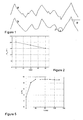
- the optical trapping capacity of a layer is given by the "Haze factor" which takes the value 0% when no part of the incident light is diffused and the value 100% when all the light received is broadcast.
- the "Haze factor” of a solar cell must have a value as high as possible, typically at least 10%.
- the values provided in the aforementioned JP document are respectively 2 to 5% before the action of an argon plasma and 0.5% after treatment. These values clearly show that the argon plasma etching of an evaporated layer does not target the field of photovoltaic cells.
- the document EP 1 443 527 discloses a textured TCO layer having a surface morphology formed of an alternation of flat depressions which have numerous micro-asperities having a base of 0.1 to 0.3 ⁇ m, a height of 0.05 to 0.2 ⁇ m and a step (distance between the vertices) of 0.1 to 0.3 ⁇ m.
- Such micro-asperities are not conducive to good subsequent growth of the photoelectric layer.
- they because of their small size, they increase little light trapping in the interesting range (red and infra-red).
- the fact that the recesses are flat has the disadvantage of increasing the reflection of the light and thereby reduce the light injected into the photovoltaic device, thereby reducing the photo-generated current.
- One of the aims of the present invention is to provide a TCO layer having a good light-trapping capacity while ensuring satisfactory subsequent growth of the photoelectric layer.
- a photoelectric device whether it be a solar cell or a photodetector, is characterized by its efficiency. conversion ⁇ and its optical trapping capacity, the first depending on the second, as long as the collection of the photo-generated current is good.
- the method according to the invention comprises two essential operations, performed on a substrate for a photoelectric device, which may be plastic, metal, glass or any other insulating or conductive, flexible or rigid material.
- the first operation is the deposition, on the substrate, of a transparent conductive oxide layer TCO, consisting in particular of SnO 2 , ZnO, ITO, In 2 O 3 , Cd 2 SnO 4 , or a combination of these oxides, typically having a thickness of about 0.05 to 10 microns.
- a transparent conductive oxide layer TCO consisting in particular of SnO 2 , ZnO, ITO, In 2 O 3 , Cd 2 SnO 4 , or a combination of these oxides, typically having a thickness of about 0.05 to 10 microns.
- the deposition is carried out chemically, this expression encompassing processes that are in themselves physical but in which a chemical reaction takes place.
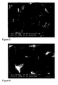
- this layer has a very rough surface made of bumps and depressions, which are generally V-shaped with relatively steep sides.
- the radius of curvature p of these hollows is, typically, a few nanometers.
- Such a morphology proves unsuitable for good subsequent growth, from it, of the photoelectric layer which will make it a solar cell or a photodetector with good conversion efficiency.
- the valleys of the V are favorable places, during the growth of the semiconductor layers, the appearance of cracks or cracks may cause carrier recombination and other electrical problems (short circuit, .... ) that affect the conversion efficiency of the device.
- the roughness of the chemically deposited TCO layer can be characterized by the standard deviation of the heights of the points constituting its surface "rms-roughness" whose value, shown on the graph of the figure 2 is 202 nm.
- the method according to the present invention corrects this weakness by means of a second operation which consists of an attack of the TCO layer using a rare gas plasma, such as helium (He), neon (Ne), argon (Ar), krypton (Kr), xenon (Xe) and radon (Rn).
- a rare gas plasma such as helium (He), neon (Ne), argon (Ar), krypton (Kr), xenon (Xe) and radon (Rn).
- a simple atmospheric attack provides the desired effect.
- the attack can be done using at least one other gas such as hydrogen (H 2 ), oxygen (O 2 ), nitrogen (N 2 ), chlorine (Cl 2 ), methane (CH 4 ), water (H 2 O) and carbon dioxide (CO 2 ).
- the attack is performed by an argon plasma.
- the bottoms are practically smooth, that is to say that, if they have micro-asperities, they have, on average, a height less than 5 nm and a surface roughness, determined by the standard deviation of the heights of the points constituting its surface, less than 3 nm.
- Such a morphology is ideal for good subsequent growth of the photoelectric layer that will make it a solar cell or photodetector free of cracks.
- angle ⁇ formed by the flanks of the layer it should be noted that a value of less than 30 ° gives low optical trapping, while a value greater than 75 ° causes poor growth of the layer deposited by the layer. after.
- the initial layer TCO deposited chemically, which had a good optical trapping capacity, but a morphology unsuitable for good subsequent growth of the photoelectric layer always has through its plasma attack, both a good ability to trapping and a morphology well suited to the growth of the photoelectric layer.
- the graph of the figure 5 which shows the improvement, as a function of the duration t of the plasma etching, of the conversion efficiency ⁇ of a hydrogenated microcrystalline silicon photoelectric device provided with a substrate coated with a chemically deposited TCO layer.
- the microcrystalline silicon layers are deposited by the PECVD method (it should be noted that the value of ⁇ before the attack is only 3.3% at baseline but it rises to 9.2% after 40 minutes to remain constant then an optimal duration of plasma treatment under the aforementioned operating conditions is therefore about 40 minutes.
- the standard deviation of the roughness does not down to a value below 180 nm, still quite satisfactory for optimal trapping of light in the cell.
- the production yield of the layer obtained by the process according to the invention is greater than 95% whereas it is 60%, on average, when uses other methods. This is due to the fact that the plasma treatment effectively eliminates all the dust and particles present in the working environment, which could short-circuit the cells.
Landscapes
- Photovoltaic Devices (AREA)
- Non-Insulated Conductors (AREA)
- Manufacturing Of Electric Cables (AREA)
- Electrical Discharge Machining, Electrochemical Machining, And Combined Machining (AREA)
- Laminated Bodies (AREA)
Claims (10)
- Texturierte transparente leitende Schicht, die auf einem Substrat aufgebracht ist, das für einen photoelektrische Vorrichtung bestimmt ist und eine Oberflächenmorphologie aufweist, die von abwechselnden Erhebungen und Vertiefungen geformt wird, dadurch gekennzeichnet, dass:- ihre Vertiefungen einen abgerundeten Boden haben, dessen Radius größer als 25 nm ist,- die Vertiefungen praktisch glatt sind, das heißt, dass, wenn sie Mikro-Unebenheiten aufweisen, diese im Durchschnitt eine Höhe von unter 5 nm haben, und- ihre Seiten mit der Substratebene einen Winkel bilden, dessen Mediane des absoluten Werts zwischen 30° und 75° inklusive ist.
- Leitende Schicht nach Anspruch 1, dadurch gekennzeichnet, dass ihre Rauheit, die durch die Standardabweichung der Höhen der Punkte bestimmt wird, die ihre Oberfläche bilden, zwischen 40 und 250 nm inklusive ist.
- Leitende Schicht nach Anspruch 2, dadurch gekennzeichnet, dass die Rauheit ihrer Vertiefungen, die durch die Standardabweichung der Höhen der Punkte bestimmt wird, die ihre Oberfläche bilden, unter 3 nm ist.
- Leitende Schicht nach einem der Ansprüche 1 bis 3, dadurch gekennzeichnet, dass die Spanne zwischen ihren Erhebungen und ihren Vertiefungen zwischen 100 und 800 nm inklusive ist.
- Leitende Schicht nach einem der Ansprüche 1 bis 4, dadurch gekennzeichnet, dass der Abstand zwischen den Gipfeln ihrer Erhebungen zwischen 100 und 1500 nm inklusive ist.
- Verfahren zur Herstellung einer texturierten transparenten leitenden Schicht auf einem für eine photoelektrische Vorrichtung bestimmten Substrat, dadurch gekennzeichnet, dass es die folgenden wesentlichen Schritte umfasst:- Aufbringen einer rauen, lichtstreuenden Schicht auf chemischem Weg auf das Substrat,- Angreifen dieser rauen Schicht durch ein Plasma, um eine Schicht zu erhalten, die eine Oberflächenmorphologie aufweist, die von abwechselnden Erhebungen und Vertiefungen geformt wird, wobeium der Schicht eine Morphologie zu verleihen, die für ein späteres gutes Wachstum einer auf ihr aufgebrachten photoelektrischen Schicht günstig ist, ohne signifikante Verringerung ihrer Fähigkeit, das einfallende Licht zu streuen.- die Vertiefungen einen abgerundeten Boden haben, dessen Radius größer als 25 nm ist,- die Vertiefungen praktisch glatt sind, das heißt, dass, wenn sie Mikro-Unebenheiten aufweisen, diese im Durchschnitt eine Höhe von unter 5 nm haben, und- die Seiten der Schicht mit der Substratebene einen Winkel bilden, dessen Mediane des absoluten Werts zwischen 30° und 75° inklusive ist,
- Verfahren nach Anspruch 6, dadurch gekennzeichnet, dass der Schritt des Aufbringens auf chemischem Weg anhand einer der Techniken der Gruppe erfolgt, die umfasst: Niederdruck-CVD (LPCVD), Normaldruck-CVD (APCVD), metallorganische lichtinduzierte CVD (MOCVD), chemisches Sol-Gel-Bad (CBD), reaktive Verdampfung, plasmaunterstützte CVD (PECVD), Dampfstrahl, Pyrolyse durch Verdampfung und RF-Magnetron-Pulverisierung.
- Verfahren nach einem der Ansprüche 6 und 7, dadurch gekennzeichnet, dass die Schicht ein Oxid umfasst, das aus der Gruppe Sn02, ZnO, ITO, In2O3, Cd2Sn04 sowie einer Kombination dieser Oxide ausgewählt ist.
- Verfahren nach einem der Ansprüche 6 bis 8, dadurch gekennzeichnet, dass der Schritt des Angreifens mit Hilfe eines Gasplasmas erfolgt, das aus der Gruppe ausgewählt ist, die das Helium, das Neon, das Argon, das Krypton, das Xenon und das Radon umfasst.
- Verfahren nach Anspruch 9, dadurch gekennzeichnet, dass das Gas von mindestens einem anderen Gas begleitet wird, das aus der Gruppe ausgewählt ist, die den Wasserstoff, den Sauerstoff, den Stickstoff, das Chlor, das Methan, das Wasser und das Kohlendioxid umfasst.
Priority Applications (1)
| Application Number | Priority Date | Filing Date | Title |
|---|---|---|---|
| EP07704549A EP2005473B1 (de) | 2006-03-30 | 2007-02-13 | Texturierte transparente leitfähige schicht und herstellungsverfahren dafür |
Applications Claiming Priority (3)
| Application Number | Priority Date | Filing Date | Title |
|---|---|---|---|
| EP06112013A EP1840966A1 (de) | 2006-03-30 | 2006-03-30 | Transparente, leitende und strukturierte Schicht sowie Verfahren zu ihrer Herstellung |
| EP07704549A EP2005473B1 (de) | 2006-03-30 | 2007-02-13 | Texturierte transparente leitfähige schicht und herstellungsverfahren dafür |
| PCT/EP2007/051375 WO2007113037A1 (fr) | 2006-03-30 | 2007-02-13 | Couche conductrice transparente et texturee et son procede de realisation |
Publications (2)
| Publication Number | Publication Date |
|---|---|
| EP2005473A1 EP2005473A1 (de) | 2008-12-24 |
| EP2005473B1 true EP2005473B1 (de) | 2010-04-07 |
Family
ID=36545206
Family Applications (2)
| Application Number | Title | Priority Date | Filing Date |
|---|---|---|---|
| EP06112013A Withdrawn EP1840966A1 (de) | 2006-03-30 | 2006-03-30 | Transparente, leitende und strukturierte Schicht sowie Verfahren zu ihrer Herstellung |
| EP07704549A Revoked EP2005473B1 (de) | 2006-03-30 | 2007-02-13 | Texturierte transparente leitfähige schicht und herstellungsverfahren dafür |
Family Applications Before (1)
| Application Number | Title | Priority Date | Filing Date |
|---|---|---|---|
| EP06112013A Withdrawn EP1840966A1 (de) | 2006-03-30 | 2006-03-30 | Transparente, leitende und strukturierte Schicht sowie Verfahren zu ihrer Herstellung |
Country Status (10)
| Country | Link |
|---|---|
| US (1) | US8723020B2 (de) |
| EP (2) | EP1840966A1 (de) |
| JP (1) | JP2009531842A (de) |
| KR (1) | KR101504553B1 (de) |
| CN (1) | CN101410980B (de) |
| AT (1) | ATE463842T1 (de) |
| AU (1) | AU2007233965B2 (de) |
| DE (1) | DE602007005787D1 (de) |
| ES (1) | ES2343378T3 (de) |
| WO (1) | WO2007113037A1 (de) |
Families Citing this family (18)
| Publication number | Priority date | Publication date | Assignee | Title |
|---|---|---|---|---|
| JP5243697B2 (ja) * | 2006-04-19 | 2013-07-24 | 株式会社カネカ | 光電変換装置用透明導電膜とその製造方法 |
| EP2190024A1 (de) * | 2008-11-19 | 2010-05-26 | Université de Neuchâtel | Fotoelektrische Vorrichtung mit Multi-Schnittstellen und ihr Umsetzungsverfahren |
| KR20120003859A (ko) * | 2009-03-17 | 2012-01-11 | 아이엠이씨 | 플라즈마 텍스처링 방법 |
| AU2010348488B2 (en) * | 2010-03-15 | 2013-06-13 | Sharp Kabushiki Kaisha | Substrate for photoelectric conversion device, photoelectric conversion device using the substrate, and method for producing the substrate and device |
| EP2413373A1 (de) * | 2010-07-29 | 2012-02-01 | Ecole Polytechnique Fédérale de Lausanne (EPFL) | Photoelektrische Vorrichtung mit mehreren Verbindungselementen und Herstellungsverfahren dafür |
| US9276142B2 (en) | 2010-12-17 | 2016-03-01 | First Solar, Inc. | Methods for forming a transparent oxide layer for a photovoltaic device |
| US8476105B2 (en) | 2010-12-22 | 2013-07-02 | General Electric Company | Method of making a transparent conductive oxide layer and a photovoltaic device |
| EP2518789B1 (de) * | 2011-04-18 | 2016-04-13 | Corning Precision Materials Co., Ltd. | Herstellungsverfahren eines Lichtextraktionssubstrats für eine Elektrolumineszenzvorrichtung |
| KR101225739B1 (ko) * | 2011-04-22 | 2013-01-23 | 삼성코닝정밀소재 주식회사 | 광전지용 산화아연계 투명 도전막 및 그 제조방법 |
| KR101202746B1 (ko) | 2011-04-22 | 2012-11-19 | 삼성코닝정밀소재 주식회사 | 광전지 모듈용 기판 제조방법 |
| JP2013041996A (ja) * | 2011-08-16 | 2013-02-28 | Kaneka Corp | 薄膜光電変換装置 |
| KR101324725B1 (ko) * | 2012-02-21 | 2013-11-05 | 삼성코닝정밀소재 주식회사 | 투명 도전막 제조방법 |
| KR101421026B1 (ko) * | 2012-06-12 | 2014-07-22 | 코닝정밀소재 주식회사 | 유기발광소자용 광추출층 기판 및 그 제조방법 |
| RU2505888C1 (ru) * | 2012-07-31 | 2014-01-27 | Федеральное государственное бюджетное учреждение науки Физико-технический институт им. А.Ф. Иоффе Российской академии наук | Способ получения слоя прозрачного проводящего оксида на стеклянной подложке |
| CN103236451A (zh) * | 2013-04-10 | 2013-08-07 | 中国科学院微电子研究所 | 结合氧化锌纳米线的硅超小绒面太阳电池及其制备方法 |
| CN104201235B (zh) * | 2014-07-16 | 2017-04-05 | 电子科技大学 | 一种薄膜太阳能电池azo薄膜的等离子体织构方法 |
| CN104465814B (zh) * | 2014-12-15 | 2017-04-05 | 中国科学院微电子研究所 | 一种结合氧化锌纳米结构超小绒面太阳电池及其制备方法 |
| CN110137233B (zh) | 2019-05-28 | 2022-01-14 | 合肥京东方显示技术有限公司 | 阵列基板及其制备方法、显示装置 |
Family Cites Families (18)
| Publication number | Priority date | Publication date | Assignee | Title |
|---|---|---|---|---|
| JPS5137155B2 (de) * | 1973-03-12 | 1976-10-14 | ||
| US4532537A (en) * | 1982-09-27 | 1985-07-30 | Rca Corporation | Photodetector with enhanced light absorption |
| JPH0682625B2 (ja) | 1985-06-04 | 1994-10-19 | シーメンス ソーラー インダストリーズ,エル.ピー. | 酸化亜鉛膜の蒸着方法 |
| JPS61288473A (ja) * | 1985-06-17 | 1986-12-18 | Sanyo Electric Co Ltd | 光起電力装置 |
| JPS62297462A (ja) | 1986-06-18 | 1987-12-24 | Toyota Motor Corp | 高速真空成膜方法 |
| JPH04133360A (ja) * | 1990-09-25 | 1992-05-07 | Sanyo Electric Co Ltd | 光起電力装置 |
| JPH06132533A (ja) * | 1992-10-19 | 1994-05-13 | Toshiba Corp | Tftアレイ基板の製造方法 |
| JP3651932B2 (ja) * | 1994-08-24 | 2005-05-25 | キヤノン株式会社 | 光起電力素子用裏面反射層及びその形成方法並びに光起電力素子及びその製造方法 |
| DE19713215A1 (de) | 1997-03-27 | 1998-10-08 | Forschungszentrum Juelich Gmbh | Solarzelle mit texturierter TCO-Schicht sowie Verfahren zur Herstellung einer solchen TCO-Schicht für eine solche Solarzelle |
| NL1013900C2 (nl) * | 1999-12-21 | 2001-06-25 | Akzo Nobel Nv | Werkwijze voor de vervaardiging van een zonnecelfolie met in serie geschakelde zonnecellen. |
| JP2001352086A (ja) * | 2000-06-06 | 2001-12-21 | Mitsubishi Heavy Ind Ltd | 透明電極膜、その製造方法、および該透明電極膜を用いた太陽電池及びその製造方法 |
| US6787692B2 (en) * | 2000-10-31 | 2004-09-07 | National Institute Of Advanced Industrial Science & Technology | Solar cell substrate, thin-film solar cell, and multi-junction thin-film solar cell |
| US6750394B2 (en) * | 2001-01-12 | 2004-06-15 | Sharp Kabushiki Kaisha | Thin-film solar cell and its manufacturing method |
| US20030044539A1 (en) * | 2001-02-06 | 2003-03-06 | Oswald Robert S. | Process for producing photovoltaic devices |
| EP1289025A1 (de) * | 2001-08-30 | 2003-03-05 | Universite De Neuchatel | Abscheidungsverfahren von einer Oxydschicht auf einem Substrat und dieses verwendende photovoltaische Zelle |
| JP4389585B2 (ja) * | 2001-10-19 | 2009-12-24 | 旭硝子株式会社 | 透明導電性酸化物膜付き基体および光電変換素子 |
| US20050172997A1 (en) * | 2004-02-06 | 2005-08-11 | Johannes Meier | Back contact and back reflector for thin film silicon solar cells |
| JP2005347490A (ja) * | 2004-06-02 | 2005-12-15 | Asahi Glass Co Ltd | 透明導電性酸化物膜付き基体およびその製造方法ならびに光電変換素子 |
-
2006
- 2006-03-30 EP EP06112013A patent/EP1840966A1/de not_active Withdrawn
-
2007
- 2007-02-13 KR KR1020087025467A patent/KR101504553B1/ko not_active Expired - Fee Related
- 2007-02-13 WO PCT/EP2007/051375 patent/WO2007113037A1/fr not_active Ceased
- 2007-02-13 ES ES07704549T patent/ES2343378T3/es active Active
- 2007-02-13 JP JP2009501977A patent/JP2009531842A/ja active Pending
- 2007-02-13 AT AT07704549T patent/ATE463842T1/de not_active IP Right Cessation
- 2007-02-13 EP EP07704549A patent/EP2005473B1/de not_active Revoked
- 2007-02-13 DE DE602007005787T patent/DE602007005787D1/de active Active
- 2007-02-13 AU AU2007233965A patent/AU2007233965B2/en not_active Ceased
- 2007-02-13 US US12/294,936 patent/US8723020B2/en not_active Expired - Fee Related
- 2007-02-13 CN CN2007800112081A patent/CN101410980B/zh not_active Expired - Fee Related
Also Published As
| Publication number | Publication date |
|---|---|
| AU2007233965A1 (en) | 2007-10-11 |
| AU2007233965B2 (en) | 2012-03-29 |
| EP1840966A1 (de) | 2007-10-03 |
| JP2009531842A (ja) | 2009-09-03 |
| ATE463842T1 (de) | 2010-04-15 |
| EP2005473A1 (de) | 2008-12-24 |
| US20100126575A1 (en) | 2010-05-27 |
| WO2007113037A1 (fr) | 2007-10-11 |
| KR20090015898A (ko) | 2009-02-12 |
| DE602007005787D1 (de) | 2010-05-20 |
| CN101410980A (zh) | 2009-04-15 |
| KR101504553B1 (ko) | 2015-03-23 |
| CN101410980B (zh) | 2012-11-07 |
| US8723020B2 (en) | 2014-05-13 |
| ES2343378T3 (es) | 2010-07-29 |
Similar Documents
| Publication | Publication Date | Title |
|---|---|---|
| EP2005473B1 (de) | Texturierte transparente leitfähige schicht und herstellungsverfahren dafür | |
| JP5156641B2 (ja) | 光電変換装置用透明導電膜付基板及び光電変換装置の製造方法 | |
| EP2110859B1 (de) | Fotoelektrischer wandler des laminattyps und verfahren zu seiner herstellung | |
| US5603778A (en) | Method of forming transparent conductive layer, photoelectric conversion device using the transparent conductive layer, and manufacturing method for the photoelectric conversion device | |
| EP2905814B1 (de) | Verfahren zur herstellung einer kristallinen siliciumsolarzelle, und verfahren zur herstellung eines solarzellenmoduls | |
| JPWO2008078471A1 (ja) | 光電変換装置及びその製造方法 | |
| EP2159851A1 (de) | Verfahren zur Beschränkung des epitaxialen Wachstums in einer fotoelektrischen Vorrichtung mit Heteroübergängen und eine solche fotoelektrische Vorrichtung | |
| JP2962897B2 (ja) | 光起電力素子 | |
| JP4904311B2 (ja) | 薄膜光電変換装置用透明導電膜付き基板の製造方法 | |
| JP2013542317A (ja) | 太陽電池を製造するための基板をコーティングする方法 | |
| JP2007288043A (ja) | 光電変換装置用透明導電膜とその製造方法 | |
| EP2190023A1 (de) | Fotoelektrische Vorrichtung mit Multi-Schnittstellen und ihr Umsetzungsverfahren | |
| TW201131797A (en) | Method for manufacturing a thin-film, silicon based solar cell device | |
| JP2013191587A (ja) | 裏面電極、裏面電極の製造方法、及び薄膜太陽電池 | |
| EP2521183A2 (de) | Fotovoltaikzelle, die über eine Pufferschicht aus Zinkoxid(en) und Zinn verfügt | |
| JP2000252504A (ja) | シリコン系薄膜光電変換装置およびその製造方法 | |
| WO2011033072A2 (en) | High-efficiency amorphous silicon photovoltaic devices | |
| WO2011158645A1 (ja) | 薄膜太陽電池 | |
| Jia et al. | Highly-transparent ZnO: Ga through rapid thermal annealing for low-bandgap solar cell application | |
| EP2543073A2 (de) | Transparentes leitfähiges substrat für optoelektronische bauelemente | |
| JP2011198964A (ja) | 薄膜光電変換装置およびその製造方法 | |
| Hotovy et al. | Influence of deposition parameters of sputtered ITO/Ag back contacts on the performance of a-Si: H/µc-Si: H solar cells | |
| JP2013041996A (ja) | 薄膜光電変換装置 | |
| JP2013012593A (ja) | 薄膜光電変換装置 |
Legal Events
| Date | Code | Title | Description |
|---|---|---|---|
| PUAI | Public reference made under article 153(3) epc to a published international application that has entered the european phase |
Free format text: ORIGINAL CODE: 0009012 |
|
| 17P | Request for examination filed |
Effective date: 20081021 |
|
| AK | Designated contracting states |
Kind code of ref document: A1 Designated state(s): AT BE BG CH CY CZ DE DK EE ES FI FR GB GR HU IE IS IT LI LT LU LV MC NL PL PT RO SE SI SK TR |
|
| GRAJ | Information related to disapproval of communication of intention to grant by the applicant or resumption of examination proceedings by the epo deleted |
Free format text: ORIGINAL CODE: EPIDOSDIGR1 |
|
| GRAP | Despatch of communication of intention to grant a patent |
Free format text: ORIGINAL CODE: EPIDOSNIGR1 |
|
| RIC1 | Information provided on ipc code assigned before grant |
Ipc: H01L 31/0236 20060101ALI20090622BHEP Ipc: H01L 27/142 20060101AFI20090622BHEP Ipc: H01L 31/18 20060101ALI20090622BHEP |
|
| RIN1 | Information on inventor provided before grant (corrected) |
Inventor name: DOMINE, DIDIER Inventor name: BALLIF, CHRISTOPHE Inventor name: BAILAT, JULIEN |
|
| GRAS | Grant fee paid |
Free format text: ORIGINAL CODE: EPIDOSNIGR3 |
|
| GRAA | (expected) grant |
Free format text: ORIGINAL CODE: 0009210 |
|
| AK | Designated contracting states |
Kind code of ref document: B1 Designated state(s): AT BE BG CH CY CZ DE DK EE ES FI FR GB GR HU IE IS IT LI LT LU LV MC NL PL PT RO SE SI SK TR |
|
| REG | Reference to a national code |
Ref country code: GB Ref legal event code: FG4D Free format text: NOT ENGLISH |
|
| REG | Reference to a national code |
Ref country code: CH Ref legal event code: EP |
|
| REG | Reference to a national code |
Ref country code: IE Ref legal event code: FG4D Free format text: LANGUAGE OF EP DOCUMENT: FRENCH |
|
| REF | Corresponds to: |
Ref document number: 602007005787 Country of ref document: DE Date of ref document: 20100520 Kind code of ref document: P |
|
| REG | Reference to a national code |
Ref country code: CH Ref legal event code: NV Representative=s name: GLN S.A. |
|
| REG | Reference to a national code |
Ref country code: GR Ref legal event code: EP Ref document number: 20100401519 Country of ref document: GR |
|
| REG | Reference to a national code |
Ref country code: NL Ref legal event code: VDEP Effective date: 20100407 |
|
| REG | Reference to a national code |
Ref country code: ES Ref legal event code: FG2A Ref document number: 2343378 Country of ref document: ES Kind code of ref document: T3 |
|
| PG25 | Lapsed in a contracting state [announced via postgrant information from national office to epo] |
Ref country code: SI Free format text: LAPSE BECAUSE OF FAILURE TO SUBMIT A TRANSLATION OF THE DESCRIPTION OR TO PAY THE FEE WITHIN THE PRESCRIBED TIME-LIMIT Effective date: 20100407 |
|
| LTIE | Lt: invalidation of european patent or patent extension |
Effective date: 20100407 |
|
| REG | Reference to a national code |
Ref country code: IE Ref legal event code: FD4D |
|
| PG25 | Lapsed in a contracting state [announced via postgrant information from national office to epo] |
Ref country code: NL Free format text: LAPSE BECAUSE OF FAILURE TO SUBMIT A TRANSLATION OF THE DESCRIPTION OR TO PAY THE FEE WITHIN THE PRESCRIBED TIME-LIMIT Effective date: 20100407 Ref country code: LT Free format text: LAPSE BECAUSE OF FAILURE TO SUBMIT A TRANSLATION OF THE DESCRIPTION OR TO PAY THE FEE WITHIN THE PRESCRIBED TIME-LIMIT Effective date: 20100407 Ref country code: SE Free format text: LAPSE BECAUSE OF FAILURE TO SUBMIT A TRANSLATION OF THE DESCRIPTION OR TO PAY THE FEE WITHIN THE PRESCRIBED TIME-LIMIT Effective date: 20100407 |
|
| PG25 | Lapsed in a contracting state [announced via postgrant information from national office to epo] |
Ref country code: AT Free format text: LAPSE BECAUSE OF FAILURE TO SUBMIT A TRANSLATION OF THE DESCRIPTION OR TO PAY THE FEE WITHIN THE PRESCRIBED TIME-LIMIT Effective date: 20100407 Ref country code: IS Free format text: LAPSE BECAUSE OF FAILURE TO SUBMIT A TRANSLATION OF THE DESCRIPTION OR TO PAY THE FEE WITHIN THE PRESCRIBED TIME-LIMIT Effective date: 20100807 Ref country code: LV Free format text: LAPSE BECAUSE OF FAILURE TO SUBMIT A TRANSLATION OF THE DESCRIPTION OR TO PAY THE FEE WITHIN THE PRESCRIBED TIME-LIMIT Effective date: 20100407 Ref country code: FI Free format text: LAPSE BECAUSE OF FAILURE TO SUBMIT A TRANSLATION OF THE DESCRIPTION OR TO PAY THE FEE WITHIN THE PRESCRIBED TIME-LIMIT Effective date: 20100407 |
|
| PG25 | Lapsed in a contracting state [announced via postgrant information from national office to epo] |
Ref country code: PL Free format text: LAPSE BECAUSE OF FAILURE TO SUBMIT A TRANSLATION OF THE DESCRIPTION OR TO PAY THE FEE WITHIN THE PRESCRIBED TIME-LIMIT Effective date: 20100407 Ref country code: CY Free format text: LAPSE BECAUSE OF FAILURE TO SUBMIT A TRANSLATION OF THE DESCRIPTION OR TO PAY THE FEE WITHIN THE PRESCRIBED TIME-LIMIT Effective date: 20100602 |
|
| PLBI | Opposition filed |
Free format text: ORIGINAL CODE: 0009260 |
|
| PG25 | Lapsed in a contracting state [announced via postgrant information from national office to epo] |
Ref country code: DK Free format text: LAPSE BECAUSE OF FAILURE TO SUBMIT A TRANSLATION OF THE DESCRIPTION OR TO PAY THE FEE WITHIN THE PRESCRIBED TIME-LIMIT Effective date: 20100407 Ref country code: PT Free format text: LAPSE BECAUSE OF FAILURE TO SUBMIT A TRANSLATION OF THE DESCRIPTION OR TO PAY THE FEE WITHIN THE PRESCRIBED TIME-LIMIT Effective date: 20100809 Ref country code: IE Free format text: LAPSE BECAUSE OF FAILURE TO SUBMIT A TRANSLATION OF THE DESCRIPTION OR TO PAY THE FEE WITHIN THE PRESCRIBED TIME-LIMIT Effective date: 20100407 Ref country code: EE Free format text: LAPSE BECAUSE OF FAILURE TO SUBMIT A TRANSLATION OF THE DESCRIPTION OR TO PAY THE FEE WITHIN THE PRESCRIBED TIME-LIMIT Effective date: 20100407 |
|
| PLAX | Notice of opposition and request to file observation + time limit sent |
Free format text: ORIGINAL CODE: EPIDOSNOBS2 |
|
| 26 | Opposition filed |
Opponent name: SCHOTT AG / SCHOTT SOLAR THIN FILM GMBH Effective date: 20110103 Opponent name: EUROGLAS GMBH Effective date: 20110107 |
|
| PG25 | Lapsed in a contracting state [announced via postgrant information from national office to epo] |
Ref country code: SK Free format text: LAPSE BECAUSE OF FAILURE TO SUBMIT A TRANSLATION OF THE DESCRIPTION OR TO PAY THE FEE WITHIN THE PRESCRIBED TIME-LIMIT Effective date: 20100407 Ref country code: CZ Free format text: LAPSE BECAUSE OF FAILURE TO SUBMIT A TRANSLATION OF THE DESCRIPTION OR TO PAY THE FEE WITHIN THE PRESCRIBED TIME-LIMIT Effective date: 20100407 Ref country code: RO Free format text: LAPSE BECAUSE OF FAILURE TO SUBMIT A TRANSLATION OF THE DESCRIPTION OR TO PAY THE FEE WITHIN THE PRESCRIBED TIME-LIMIT Effective date: 20100407 |
|
| PLAF | Information modified related to communication of a notice of opposition and request to file observations + time limit |
Free format text: ORIGINAL CODE: EPIDOSCOBS2 |
|
| PLBB | Reply of patent proprietor to notice(s) of opposition received |
Free format text: ORIGINAL CODE: EPIDOSNOBS3 |
|
| REG | Reference to a national code |
Ref country code: CH Ref legal event code: PCOW Free format text: UNIVERSITE DE NEUCHATEL;FAUBOURG DU LAC 5A;2000 NEUCHATEL (CH) |
|
| BERE | Be: lapsed |
Owner name: UNIVERSITE DE NEUCHATEL Effective date: 20110228 |
|
| PG25 | Lapsed in a contracting state [announced via postgrant information from national office to epo] |
Ref country code: MC Free format text: LAPSE BECAUSE OF NON-PAYMENT OF DUE FEES Effective date: 20110228 |
|
| RAP2 | Party data changed (patent owner data changed or rights of a patent transferred) |
Owner name: UNIVERSITE DE NEUCHATEL |
|
| GBPC | Gb: european patent ceased through non-payment of renewal fee |
Effective date: 20110213 |
|
| REG | Reference to a national code |
Ref country code: FR Ref legal event code: ST Effective date: 20111102 |
|
| PG25 | Lapsed in a contracting state [announced via postgrant information from national office to epo] |
Ref country code: BE Free format text: LAPSE BECAUSE OF NON-PAYMENT OF DUE FEES Effective date: 20110228 |
|
| PG25 | Lapsed in a contracting state [announced via postgrant information from national office to epo] |
Ref country code: FR Free format text: LAPSE BECAUSE OF NON-PAYMENT OF DUE FEES Effective date: 20110228 |
|
| PG25 | Lapsed in a contracting state [announced via postgrant information from national office to epo] |
Ref country code: GB Free format text: LAPSE BECAUSE OF NON-PAYMENT OF DUE FEES Effective date: 20110213 |
|
| PGFP | Annual fee paid to national office [announced via postgrant information from national office to epo] |
Ref country code: CH Payment date: 20120224 Year of fee payment: 6 |
|
| PGFP | Annual fee paid to national office [announced via postgrant information from national office to epo] |
Ref country code: DE Payment date: 20120228 Year of fee payment: 6 |
|
| PGFP | Annual fee paid to national office [announced via postgrant information from national office to epo] |
Ref country code: GR Payment date: 20120228 Year of fee payment: 6 Ref country code: IT Payment date: 20120223 Year of fee payment: 6 |
|
| RDAF | Communication despatched that patent is revoked |
Free format text: ORIGINAL CODE: EPIDOSNREV1 |
|
| REG | Reference to a national code |
Ref country code: DE Ref legal event code: R103 Ref document number: 602007005787 Country of ref document: DE Ref country code: DE Ref legal event code: R064 Ref document number: 602007005787 Country of ref document: DE |
|
| RDAG | Patent revoked |
Free format text: ORIGINAL CODE: 0009271 |
|
| STAA | Information on the status of an ep patent application or granted ep patent |
Free format text: STATUS: PATENT REVOKED |
|
| REG | Reference to a national code |
Ref country code: CH Ref legal event code: PL |
|
| 27W | Patent revoked |
Effective date: 20120712 |
|
| REG | Reference to a national code |
Ref country code: DE Ref legal event code: R107 Ref document number: 602007005787 Country of ref document: DE Effective date: 20130110 |
|
| PG25 | Lapsed in a contracting state [announced via postgrant information from national office to epo] |
Ref country code: LI Free format text: LAPSE BECAUSE OF THE APPLICANT RENOUNCES Effective date: 20100407 Ref country code: CH Free format text: LAPSE BECAUSE OF THE APPLICANT RENOUNCES Effective date: 20100407 |
|
| PGFP | Annual fee paid to national office [announced via postgrant information from national office to epo] |
Ref country code: ES Payment date: 20120227 Year of fee payment: 6 |
|
| PG25 | Lapsed in a contracting state [announced via postgrant information from national office to epo] |
Ref country code: BG Free format text: LAPSE BECAUSE OF FAILURE TO SUBMIT A TRANSLATION OF THE DESCRIPTION OR TO PAY THE FEE WITHIN THE PRESCRIBED TIME-LIMIT Effective date: 20100707 |
|
| REG | Reference to a national code |
Ref country code: GR Ref legal event code: ML Ref document number: 20100401519 Country of ref document: GR Effective date: 20130904 |
|
| PG25 | Lapsed in a contracting state [announced via postgrant information from national office to epo] |
Ref country code: HU Free format text: LAPSE BECAUSE OF FAILURE TO SUBMIT A TRANSLATION OF THE DESCRIPTION OR TO PAY THE FEE WITHIN THE PRESCRIBED TIME-LIMIT Effective date: 20100407 |
|
| PG25 | Lapsed in a contracting state [announced via postgrant information from national office to epo] |
Ref country code: LU Free format text: LAPSE BECAUSE OF NON-PAYMENT OF DUE FEES Effective date: 20110213 |