EP2048872A2 - Vorrichtung und Verfahren zum Steuern des Schwarzanteils - Google Patents
Vorrichtung und Verfahren zum Steuern des Schwarzanteils Download PDFInfo
- Publication number
- EP2048872A2 EP2048872A2 EP08253273A EP08253273A EP2048872A2 EP 2048872 A2 EP2048872 A2 EP 2048872A2 EP 08253273 A EP08253273 A EP 08253273A EP 08253273 A EP08253273 A EP 08253273A EP 2048872 A2 EP2048872 A2 EP 2048872A2
- Authority
- EP
- European Patent Office
- Prior art keywords
- signal
- black level
- image
- sensing device
- channel
- Prior art date
- Legal status (The legal status is an assumption and is not a legal conclusion. Google has not performed a legal analysis and makes no representation as to the accuracy of the status listed.)
- Ceased
Links
Images


Classifications
-
- H—ELECTRICITY
- H04—ELECTRIC COMMUNICATION TECHNIQUE
- H04N—PICTORIAL COMMUNICATION, e.g. TELEVISION
- H04N5/00—Details of television systems
- H04N5/14—Picture signal circuitry for video frequency region
- H04N5/16—Circuitry for reinsertion of DC and slowly varying components of signal; Circuitry for preservation of black or white level
- H04N5/18—Circuitry for reinsertion of DC and slowly varying components of signal; Circuitry for preservation of black or white level by means of "clamp" circuit operated by switching circuit
- H04N5/185—Circuitry for reinsertion of DC and slowly varying components of signal; Circuitry for preservation of black or white level by means of "clamp" circuit operated by switching circuit for the black level
-
- H—ELECTRICITY
- H04—ELECTRIC COMMUNICATION TECHNIQUE
- H04N—PICTORIAL COMMUNICATION, e.g. TELEVISION
- H04N5/00—Details of television systems
- H04N5/14—Picture signal circuitry for video frequency region
- H04N5/16—Circuitry for reinsertion of DC and slowly varying components of signal; Circuitry for preservation of black or white level
- H04N5/165—Circuitry for reinsertion of DC and slowly varying components of signal; Circuitry for preservation of black or white level to maintain the black level constant
-
- H—ELECTRICITY
- H04—ELECTRIC COMMUNICATION TECHNIQUE
- H04N—PICTORIAL COMMUNICATION, e.g. TELEVISION
- H04N25/00—Circuitry of solid-state image sensors [SSIS]; Control thereof
- H04N25/60—Noise processing, e.g. detecting, correcting, reducing or removing noise
- H04N25/63—Noise processing, e.g. detecting, correcting, reducing or removing noise applied to dark current
- H04N25/633—Noise processing, e.g. detecting, correcting, reducing or removing noise applied to dark current by using optical black pixels
-
- H—ELECTRICITY
- H04—ELECTRIC COMMUNICATION TECHNIQUE
- H04N—PICTORIAL COMMUNICATION, e.g. TELEVISION
- H04N25/00—Circuitry of solid-state image sensors [SSIS]; Control thereof
- H04N25/60—Noise processing, e.g. detecting, correcting, reducing or removing noise
- H04N25/67—Noise processing, e.g. detecting, correcting, reducing or removing noise applied to fixed-pattern noise, e.g. non-uniformity of response
- H04N25/671—Noise processing, e.g. detecting, correcting, reducing or removing noise applied to fixed-pattern noise, e.g. non-uniformity of response for non-uniformity detection or correction
- H04N25/673—Noise processing, e.g. detecting, correcting, reducing or removing noise applied to fixed-pattern noise, e.g. non-uniformity of response for non-uniformity detection or correction by using reference sources
Definitions
- This invention relates to a black level control apparatus and method; in particular, but not exclusively, for an electronic camera, especially a high-speed video camera.
- black level may be used to refer i) to the display input signal amplitude required for an image display device to render black in a displayed image (i.e., zero illumination to be provided by the device), or ii) to the sensor output signal amplitude generated by an image sensor when the output signal corresponds to a black region of a scene being captured (i.e., zero illumination received by the sensor).
- the term is used principally to refer to the sensor black level, unless otherwise stated or clear from the context.
- Image display devices are typically arranged with a definition that a display input signal of zero amplitude (or a fixed reference voltage, in the case of NTSC) will result in a black displayed image. This is typically also the case with image/video recording devices and digitising systems. Most image sensors, however, have no such definition, so that the sensor output signal is not necessarily of zero amplitude when all light is excluded from the sensor. The amplitude of the sensor output signal may be non-zero to a degree which is affected mainly by the design of the sensor, by manufacturing variations between sensors of the same design, and by temperature of operation.
- Coupling the sensor output signal to an image display device could therefore result in black regions of a scene being represented by an undefined and most likely non-zero luminance (brightness) in the displayed image (e.g., appearing as grey, instead of black). It is accordingly important for an electronic camera to be able to normalise the sensor output signal; that is, to determine and control the black level so that the display input signal from a camera has zero amplitude (or a fixed reference voltage) to represent black.
- the sensing array in an electronic image sensor typically represents the image by producing a complex electrical waveform.
- the waveform is sampled by the processing circuitry in synchrony with the pixel clock, to reduce contributions to the signal which do not originate from the scene being captured.
- the waveform thus typically provides a voltage which varies with the pattern and intensity of light falling on the sensor. Without black level control, the waveform will not have a fixed voltage level to represent black.
- the most common technique for providing black level control involves masking a number of pixels in the sensing array such that they have a greatly reduced sensitivity to light.
- the signal from these pixels is read out of the array to provide a voltage amplitude which is deemed to correspond to the voltage amplitude of a non-illuminated pixel in the active region of the image sensor. Accordingly, the DC voltage level of the waveform from the active region of the sensor is shifted up or down by the voltage amplitude read out from the masked region of the sensor.
- the voltage amplitude representing black may thereby be adjusted to zero (a fixed, non-zero value may alternatively be chosen).
- the information from the masked region may be read out at any suitable stage of the read-out from the array (i.e. before or after all, or part, of the information from the active region).
- the information from both regions is thereby carried in the same waveform.
- the black portion of the waveform, from the masked region is read by an electronic clamp circuit for providing the adjustment to the DC voltage level of the waveform. In this way, the remainder of the waveform is referenced to a fixed black level voltage.
- the clamp circuit comprises a driving amplifier and a capacitor, both in series with the video signal processing line, and a clamp switch, which is connected to a black level reference voltage source, which may or may not be ground (i.e. 0V).
- the clamp switch is arranged to short-circuit the video signal to the reference voltage at times when the video signal passing the clamp switch is the black portion of the waveform.
- the capacitor is charged, or discharged, in dependence upon the voltage level of the black portion.
- the clamp switch turns off, to remove the short-circuit, the potential difference across the capacitor is considered to provide the DC offset voltage between the actual image sensor output signal black level amplitude and the desired reference amplitude.
- Operation of the clamp circuit relies on a further amplifier, provided on the signal processing line downstream of the clamp switch, drawing little or no DC current, so that the clamp capacitor is only negligibly discharged before the next clamping step.
- the clamp circuit continually adjusts the DC voltage level of the sensor output signal, to take account of variations in the sensor black level with time and temperature, at a rate typically in the range from 50Hz to tens of kilohertz (e.g., if the clamping rate is at line frequency, this is 50Hz for PAL and 60Hz for NTSC; if picture frequency, this is 15.625kHz for PAL and NTSC).
- the clamp circuit operation is reasonably imprecise, as indicated above.
- the masked region of the sensor array has a greatly reduced sensitivity to light, it is typically not opaque (i.e., it does not have zero sensitivity).
- the image sensor may have multiple output channels for different regions of the sensor array. Since it is desirable to achieve fast read-out of information from the array, if a respective clamp circuit of the above type were provided on each output channel, a significant proportion of the overall read-out time would be spent reading black pixels, when information from the active pixel regions could be read.
- an image embedding process has a first image source and a second image source which are combined in an image output.
- the first source has a black level generator different to that of the image.
- the first image black level signal is detected.
- a switch provides combinations of the two images with the detected black level, and a second combination without the black level.
- US 5,070,414 relates to an image reader comprising a line sensor having an array of photoelectric conversion elements, the photoelectric conversion elements being selectively shaded to provide light-shielded pixels for outputting light-shielded signals and effective pixels which are not shaded for outputting effective pixel signals.
- Analogue-to-digital conversion means convert the light-shielded signals to digital light-shielded signals, which are then held by holding means.
- Image signal producing means correct a first signal corresponding to the effective pixel signals in accordance with a second signal corresponding to the digital light-shielded signals held by the holding means and generate an image signal.
- EP-Al-1,237,353 relates to an image sensor which includes an active pixel area for image capture, one or more black pixel areas disposed in a pre-determined, significant spaced apart distance from the active pixel area, and a light shield to prevent light from illuminating the black pixel areas.
- the invention aims to provide such a black level control technique.
- a black level control apparatus for controlling the black level of an image signal from an image sensing device, the apparatus comprising: an image signal channel for receiving an image signal from an image sensing device, the image signal having a black level; a black level sensing device for generating a black level signal; a black level signal channel for receiving the black level signal from the black level sensing device, the black level signal channel being independent from the image signal channel; a black level controller for receiving an input signal based on the black level signal, measuring a difference between the input signal and a reference signal, generating a control signal based on the difference, and outputting the control signal to the image signal channel to adjust the black level of the image signal, and feeding the control signal back to the black level signal channel, such that the input signal is based on the black level signal and the control signal.
- a black portion from the black level sensing device, may be read at any desired time. Furthermore, it is not necessary to interrupt or delay the readout of the image signal from an image sensing device, as this may be read out simultaneously.
- the control signal is fed into a black level signal channel, so that the black level control apparatus may operate as a closed-loop, feed back system to continually adjust the control signal.
- the black level sensing device is reset independently of the image sensing device. This has the benefit of allowing the shutter period of the black level sensing device to be different from the shutter period of the image sensing device.
- the black level sensing device may have a shorter shutter period, for a shorter integration time, so that the sensitivity of the black level sensing device does not rely solely on the opacity of the mask, since the short shutter period will reduce the effect of light which is inadvertently detected per shutter period.
- control signal is added to the image signal channel and the black level signal channel as an analogue signal, upstream of any signal processing stages.
- processing stages are the same for the image signal channel and the black level signal channel, so that system effects are reduced or avoided.
- differential signalling in the processing stages and/or the use of instrumentation amplifiers can also help to cancel or reduce noise.
- the reference signal is determined by calibrating the image signal to a desired black level, using a calibration control signal from the controller, and applying the calibration control signal to the black level signal and storing the resulting black level input signal received by the controller as the reference signal.
- the black level of the image signal can be adjusted to or kept at the desired black level.
- a respective black level control apparatus may be provided for each image sensing device or region thereof.
- the black level control apparatus is employed in an electronic camera; in particular, in a high-speed video camera.
- a method of controlling the black level of an image signal from an image sensing device comprising the steps of: monitoring at a black level controller a black level input signal based on a black level signal from a black level sensing device, wherein the black level sensing device is independent of the image sensing device; generating at the black level controller a control signal based on a difference between the black level input signal and a reference signal; adding the control signal to image signal to adjust the black level of the image signal; and adding the control signal to the black level signal.
- the camera 8 has an optical assembly (not shown) for receiving and focusing light onto an image sensor (also not shown) and a processing assembly for processing the resulting image information.
- the camera's output may be to a display device, a recording/storage device, or to its own memory.
- the camera 8 is directed towards a scene to be captured.
- Light from one or more objects in the scene is focused onto the image sensor of the camera by the optical assembly.
- An image of the scene is thereby formed at the sensor, which generates an image signal representative thereof.
- the image signal may then undergo various image processing steps, including black level control.
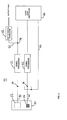
- a sensor 20 comprises an image sensor portion 22 and a separate black level sensor portion 24.
- the black level sensor portion 24 employs the same type of sensing elements as the image sensor portion 22, except that the black level sensor portion is masked to reduce its light sensitivity.
- the sensor portions 22, 24 have separate and independent channels 30, 40 for receiving an image output signal and a black level output signal respectively.
- the image signal channel 30 is connected via signal processing 32 to a node 34 with an output video signal channel 50.
- the signal processing 32 provides analogue processing to the image signal, to generate a digital image signal, typically by means of amplification, sampling and A-to-D conversion, as will be understood.
- output signal processing 52 provides digital processing to the digital image signal, to generate a video output signal for supply to a display device or recording device. Without black level control, the video output signal may not represent black regions of the image correctly for the display or recording device.
- the black level signal channel 40 is connected via signal processing 42, identical to signal processing 32, to a black level controller 60.
- the controller 60 has a control signal channel 62 which is connected to a node 64 with the image signal channel 30 and to a node 66 with the black level signal channel 40. Both nodes 64, 66 are upstream of the signal processing 32, 42.
- the controller 60 may comprise a D-to-A converter, or one may be provided on the control signal channel 62, to ensure that the signals supplied to the nodes 64, 66 are analogue signals.
- the black level controller 60 stores a reference signal corresponding to a black level input signal which is received by the controller from the black level signal channel 40 when the video output signal represents black regions of an image in a desired way (e.g. as 0V in the signal), under calibration conditions.
- the black level signal is processed to generate a black level input signal for the controller 60.
- the controller 60 compares the black level input signal with the reference signal and generates a control signal based on the difference.
- the extent of the difference indicates how far off the desired black level value of the black level signal from the black level sensor portion 24 is, and, by extension, how far off the image signal from the image sensor portion 22 is. Accordingly, the control signal is added to the image signal, along control signal channel 62 and at node 64, to adjust the DC level of the image signal up or down, so that the desired black level is obtained.
- the control signal is also added to the black level signal, at node 66, to shift the DC level of the black level signal up or down in the same manner.
- This provides a closed-loop, feedback system, which aims to bring the control signal to a substantially constant value, as the black level sensor portion 24 continues to generate a black level signal which is expected to vary only slowly with time.
- a sensor 120 comprises an image sensor portion 122 for generating an image signal in response to light falling thereon and a separate black level sensor portion 124 for generating a black level signal under substantially zero illumination.
- the black level sensor portion 124 employs identical sensing elements to the image sensor portion 122, but with a number of modifications.
- the black level sensor portion 124 is masked to reduce its sensitivity to light. This may be achieved in any suitable manner, but is generally achieved by providing a metallic coating over the surface of the black level sensor portion (silicon) substrate. Preferably, the same metal which is used to provide conductive tracks on the sensor 120 is used, so that the coating procedure is simply an additional step in the photolithography process.
- the black level sensor portion 124 is provided with its own, dedicated output channel: black level signal channel 140. This is independent of the image signal channel 130, so that reading out from the sensor 120 for black level control purposes does not take up time for reading out image information. In particular, image signal reading out and black level signal reading out may be performed simultaneously.
- the black level sensor portion 124 has a reset signal 123 which is separate and independent from the reset signal 125 for the image sensor portion 122.
- the black level sensor portion 124 may therefore have a different - in particular, shorter - shutter period from the image sensor portion 122. Providing a relatively short integration time in this way helps to reduce the sensitivity of the black level sensor portion to light even further, which is beneficial since the metallic coating typically does not provide an opaque mask.
- the black level signal channel 140 is separate from the image signal channel 130, the processing of the respective signals along the channels is the same.
- the channels 130, 140 respectively comprise an amplifier 133, 143 for providing amplification as required, a sampler 134, 144 for sampling the analogue signals, an A-to-D converter 135, 145 for digitising the signal, and an averager 136, 146 for averaging the digital signal. It may be preferable in some cases to provide the amplification on the channels 130, 140 using instrumentation amplifiers, in view of their relatively high-precision, low-noise and low-drift characteristics.
- sampler and A-to-D converter may be combined on each channel 130, 140, since this will reduce the number of chips on the PCB and ease the drive requirements for the A-to-D converter input pins. Furthermore, where noise cancellation/reduction is a concern, it is preferable to operate the amplification, sampling and A-to-D conversion stages in differential signalling mode.
- the image signal channel 130 and the black level signal channel 140 are connected between the image sensor portion 122 and the black level sensor portion 124, respectively, and a black level controller 160.
- the two channels 130, 140 are maintained separate from each other between their respective sensor portion 122, 124 and the controller 160.
- the channels 130, 140 are however DC coupled by a control signal, output from the controller 160 along control signal channel 162 and converted to an analogue signal by a D-to-A converter 163.
- the control signal is added to the channels at nodes 164, 166.
- the nodes 164, 166 are located upstream of the processing stages of the channels 130, 140, at which point the image signal and black level signal are (still) analogue signals.
- the same control signal channel 162 is arranged to supply the same control signal to both the image signal channel 120 and the black level signal channel 140.
- a node 137 is located between the digitising processing 133-135 and the averager 136 and is connected to an output video signal channel 150.
- output signal processing 152 provides digital processing to the digital image signal, to generate an output video signal for supply to a display device or recording device, or the like.
- the black level sensor portion 124 is set to have its shortest possible shutter time. This significantly reduces the sensitivity of the black level sensor portion 124 to light and is superior to relying only on the opacity of the mask, as in prior art arrangements.
- the black level sensor portion 124 generates a black level signal, which is processed along the black level signal channel 140 to provide an average value of the black level signal, as a black level input signal for the controller 160.
- the controller 160 compares the black level input signal with a predetermined reference signal and generates a control signal based on the difference. The extent of the difference indicates how far off the desired black level value of the black level signal from the black level sensor portion 124 is (due to variations in temperature of operation etc.), and, by extension, how far off the image signal from the image sensor portion 122 is.
- the control signal is output from the controller 160, along control signal channel 162, converted to an analogue signal by the D-to-A converter 163, and fed back in to the black level signal channel 140 at the node 166.
- a closed-loop control system is thereby set up to minimise (or reduce) the difference between the average of the black level signal (the black level input signal) and the reference signal.
- the control signal is added to the image signal on the image signal channel 130, at the node 164.
- the DC level of the image signal is thereby shifted up or down, so that the desired black level is reached.
- the arrangement 100 uses a closed-loop control system to feed a correction signal into the open-loop image signal processing channel.
- the output video signal supplied along the output video signal channel is therefore provided with the desired black level, for example, to be presented correctly on a display device.
- the reference signal used by the controller 160 is determined in a calibration procedure prior to normal operation. In this procedure, the sensor 120 is operated in complete darkness.
- the image signal generated by the image sensor portion 122 is processed along image signal channel 130 beyond the node 137, to the averager 136.
- the averager 136 is non-operational and the processed image signal - up until the node 137 - is supplied to the output video signal channel 150 for further processing and output to a display/recording device.
- the averager 136 may be rendered non-operational either by switching it off, or by leaving it active but simply ignoring its output.
- the averager 136 provides an average value of the image signal, as an image input signal for the controller 160.
- the controller 160 generates a calibration control signal, which is D-to-A converted by DAC 163 on control signal channel 162 and fed back into the image signal channel 130 at the node 164.
- the calibration control signal is varied in this way until the image signal has a desired black level.
- the desired black level and the manner of achieving it may be selected according to preference or application.
- the desired black level may be a non-zero voltage, but will typically be 0V.
- the indicator of the black level of the image signal may be the average value output from the averager 136.
- the variation of the calibration control signal and the judgment as to when the desired black level is reached could be performed manually/visually, it is much preferred to allow the arrangement 100 to operate as a closed-loop, feedback system.
- the desired black level is initially input to the controller 160 and the calibration control signal is varied and fed back to the node 164 and combined with the image signal until the signal received by the controller from the image signal channel 130 matches the desired black level.
- the calibration control signal is fed into the black level signal channel 140, at the node 166.
- the resulting black level input signal received by the controller 160 is stored as the reference signal for normal operation. In this way, ensuring that the black level input signal matches the reference signal and adding the control signal required to achieve this to the image signal will adjust the image signal so that any black portions of the waveform are at the desired black level for output to a display/recording device.
- a black level control loop can be provided for each portion/region, so that each has an independent reference level. Calibration may be performed as above, ensuring that the desired black level for all of the portions/regions is the same value.
Landscapes
- Engineering & Computer Science (AREA)
- Multimedia (AREA)
- Signal Processing (AREA)
- Transforming Light Signals Into Electric Signals (AREA)
- Picture Signal Circuits (AREA)
- Processing Of Color Television Signals (AREA)
Applications Claiming Priority (1)
| Application Number | Priority Date | Filing Date | Title |
|---|---|---|---|
| GB0719606.6A GB2453544B (en) | 2007-10-08 | 2007-10-08 | Black level control apparatus and method |
Publications (2)
| Publication Number | Publication Date |
|---|---|
| EP2048872A2 true EP2048872A2 (de) | 2009-04-15 |
| EP2048872A3 EP2048872A3 (de) | 2012-03-28 |
Family
ID=38739279
Family Applications (1)
| Application Number | Title | Priority Date | Filing Date |
|---|---|---|---|
| EP08253273A Ceased EP2048872A3 (de) | 2007-10-08 | 2008-10-08 | Vorrichtung und Verfahren zum Steuern des Schwarzanteils |
Country Status (4)
| Country | Link |
|---|---|
| US (1) | US8384806B2 (de) |
| EP (1) | EP2048872A3 (de) |
| JP (1) | JP2009135900A (de) |
| GB (1) | GB2453544B (de) |
Families Citing this family (6)
| Publication number | Priority date | Publication date | Assignee | Title |
|---|---|---|---|---|
| US8391634B1 (en) | 2009-04-28 | 2013-03-05 | Google Inc. | Illumination estimation for images |
| US8798393B2 (en) * | 2010-12-01 | 2014-08-05 | Google Inc. | Removing illumination variation from images |
| JP2013017040A (ja) * | 2011-07-04 | 2013-01-24 | Toshiba Corp | 画像処理装置及び固体撮像装置 |
| KR101763893B1 (ko) | 2015-06-03 | 2017-08-01 | 주식회사 굿엘이디 | 광원 유닛 및 이의 제조 방법 |
| KR102509819B1 (ko) | 2015-11-04 | 2023-03-14 | 삼성전자주식회사 | 신호 처리 장치 및 신호 처리 방법 |
| KR101990869B1 (ko) | 2016-09-29 | 2019-09-30 | (주)에이피텍 | 광원 유닛 및 이의 제조 방법 |
Citations (3)
| Publication number | Priority date | Publication date | Assignee | Title |
|---|---|---|---|---|
| US5070414A (en) | 1988-09-20 | 1991-12-03 | Kabushiki Kaisha Toshiba | Method and apparatus for reading image information formed on material |
| EP1237353A1 (de) | 2001-02-09 | 2002-09-04 | Eastman Kodak Company | Bildsensor mit schwarzen Pixeln, die räumlich verteilt zu den aktiven Bildpunkten angeordnet sind |
| FR2844418A1 (fr) | 2002-09-10 | 2004-03-12 | Siemens Vdo Automotive | Procede et dispositif de combinaison d'images |
Family Cites Families (14)
| Publication number | Priority date | Publication date | Assignee | Title |
|---|---|---|---|---|
| JPH0831991B2 (ja) * | 1984-04-17 | 1996-03-27 | オリンパス光学工業株式会社 | 固体撮像装置 |
| JPH08307775A (ja) * | 1995-05-12 | 1996-11-22 | Canon Inc | 撮像装置 |
| JPH10304133A (ja) * | 1997-04-28 | 1998-11-13 | Fuji Photo Film Co Ltd | 相関二重サンプリング回路 |
| US6750910B1 (en) * | 1998-07-15 | 2004-06-15 | Texas Instruments Incorporated | Optical black and offset correction in CCD signal processing |
| US6829007B1 (en) * | 1999-09-03 | 2004-12-07 | Texas Instruments Incorporated | Digital scheme for noise filtering of optical black and offset correction in CCD signal processing |
| US7084912B2 (en) * | 2001-09-20 | 2006-08-01 | Yuen-Shung Chieh | Method for reducing coherent row-wise and column-wise fixed pattern noise in CMOS image sensors |
| US7084911B1 (en) * | 2002-11-08 | 2006-08-01 | Eastman Kodak Company | Black level calibration method for imager with hysteresis comparison and adaptive step size |
| JP4218357B2 (ja) * | 2003-01-31 | 2009-02-04 | セイコーエプソン株式会社 | デジタルクランプ回路およびデジタルクランプ処理方法 |
| US7259787B2 (en) * | 2003-03-27 | 2007-08-21 | Eastman Kodak Company | Digital black clamp circuit in electronic imaging systems |
| JP4136775B2 (ja) * | 2003-05-02 | 2008-08-20 | キヤノン株式会社 | 補正装置、撮像装置、補正方法、コンピュータが読み取り可能な記憶媒体、及びプログラム |
| JP4333290B2 (ja) * | 2003-09-04 | 2009-09-16 | 株式会社ニコン | 黒レベル補正装置、及び電子カメラ |
| JP4144517B2 (ja) * | 2003-12-05 | 2008-09-03 | ソニー株式会社 | 固体撮像装置、撮像方法 |
| JP4649155B2 (ja) * | 2004-09-22 | 2011-03-09 | キヤノン株式会社 | 撮像装置及び撮像方法 |
| JP4554504B2 (ja) * | 2005-12-16 | 2010-09-29 | 富士通セミコンダクター株式会社 | 画像データ処理回路および画像データ処理方法 |
-
2007
- 2007-10-08 GB GB0719606.6A patent/GB2453544B/en not_active Expired - Fee Related
-
2008
- 2008-10-08 JP JP2008261733A patent/JP2009135900A/ja active Pending
- 2008-10-08 US US12/247,306 patent/US8384806B2/en active Active
- 2008-10-08 EP EP08253273A patent/EP2048872A3/de not_active Ceased
Patent Citations (3)
| Publication number | Priority date | Publication date | Assignee | Title |
|---|---|---|---|---|
| US5070414A (en) | 1988-09-20 | 1991-12-03 | Kabushiki Kaisha Toshiba | Method and apparatus for reading image information formed on material |
| EP1237353A1 (de) | 2001-02-09 | 2002-09-04 | Eastman Kodak Company | Bildsensor mit schwarzen Pixeln, die räumlich verteilt zu den aktiven Bildpunkten angeordnet sind |
| FR2844418A1 (fr) | 2002-09-10 | 2004-03-12 | Siemens Vdo Automotive | Procede et dispositif de combinaison d'images |
Also Published As
| Publication number | Publication date |
|---|---|
| GB2453544A (en) | 2009-04-15 |
| US8384806B2 (en) | 2013-02-26 |
| EP2048872A3 (de) | 2012-03-28 |
| US20090102952A1 (en) | 2009-04-23 |
| JP2009135900A (ja) | 2009-06-18 |
| GB2453544B (en) | 2012-02-29 |
| GB0719606D0 (en) | 2007-11-14 |
Similar Documents
| Publication | Publication Date | Title |
|---|---|---|
| US8553114B2 (en) | Image sensing apparatus and image sensing system | |
| US7880145B2 (en) | Radiation imaging apparatus and its driving method and program | |
| US8384806B2 (en) | Black level control apparatus and method | |
| US9482628B2 (en) | Imaging apparatus, control method therefor, and storage medium | |
| US20160270755A1 (en) | Radiation imaging apparatus and radiation imaging system | |
| US7567277B2 (en) | Image-pickup device and signal processing method for noise correction | |
| JP7353783B2 (ja) | 撮像装置とその制御方法及び撮像素子とその制御方法 | |
| CN109155827B (zh) | 高动态范围成像传感器阵列 | |
| JP2024529693A (ja) | 複数の障壁とデュアルコンバージョンゲインをもつ小面積の自己較正障壁変調画素 | |
| KR20010013305A (ko) | Cmos 영상 센서에 대한 dc 오프셋 및 이득 보정방법 및 시스템 | |
| JP4517660B2 (ja) | 固体撮像装置、画像入力装置および固体撮像素子の駆動方法 | |
| US20070214200A1 (en) | Gain calibration in EMCCD cameras | |
| EP3157248B1 (de) | Bildgebungselement, bildgebungsvorrichtung, endoskop, endoskopsystem und verfahren zur ansteuerung eines bildgebungselements | |
| JP2011029887A (ja) | 撮像装置及び制御方法 | |
| KR101107164B1 (ko) | 엑스레이 검출장치 및 이의 구동방법 | |
| US5710801A (en) | X-ray examination apparatus comprising an exposure-control system | |
| WO2010010620A1 (ja) | 光または放射線撮像装置 | |
| US20090295966A1 (en) | Solid-state imaging device and camera | |
| JP6808458B2 (ja) | 放射線撮像装置および放射線撮像システム | |
| US6683310B2 (en) | Readout technique for microbolometer array | |
| JPH0415679B2 (de) | ||
| US7236192B2 (en) | Image-sensing device | |
| EP2423962A1 (de) | Digitalbildsensorsystem mit langer Belichtung | |
| JP2012095219A (ja) | 撮像装置およびその制御方法 | |
| JP5129650B2 (ja) | 撮像装置 |
Legal Events
| Date | Code | Title | Description |
|---|---|---|---|
| PUAI | Public reference made under article 153(3) epc to a published international application that has entered the european phase |
Free format text: ORIGINAL CODE: 0009012 |
|
| AK | Designated contracting states |
Kind code of ref document: A2 Designated state(s): AT BE BG CH CY CZ DE DK EE ES FI FR GB GR HR HU IE IS IT LI LT LU LV MC MT NL NO PL PT RO SE SI SK TR |
|
| AX | Request for extension of the european patent |
Extension state: AL BA MK RS |
|
| PUAL | Search report despatched |
Free format text: ORIGINAL CODE: 0009013 |
|
| AK | Designated contracting states |
Kind code of ref document: A3 Designated state(s): AT BE BG CH CY CZ DE DK EE ES FI FR GB GR HR HU IE IS IT LI LT LU LV MC MT NL NO PL PT RO SE SI SK TR |
|
| AX | Request for extension of the european patent |
Extension state: AL BA MK RS |
|
| RIC1 | Information provided on ipc code assigned before grant |
Ipc: H04N 5/18 20060101AFI20120220BHEP Ipc: H04N 5/335 20110101ALI20120220BHEP |
|
| 17P | Request for examination filed |
Effective date: 20120928 |
|
| AKX | Designation fees paid |
Designated state(s): AT BE BG CH CY CZ DE DK EE ES FI FR GB GR HR HU IE IS IT LI LT LU LV MC MT NL NO PL PT RO SE SI SK TR |
|
| 17Q | First examination report despatched |
Effective date: 20160204 |
|
| 18R | Application refused |
Effective date: 20171209 |