EP2058942A1 - Digitaler verstärker - Google Patents
Digitaler verstärker Download PDFInfo
- Publication number
- EP2058942A1 EP2058942A1 EP07806140A EP07806140A EP2058942A1 EP 2058942 A1 EP2058942 A1 EP 2058942A1 EP 07806140 A EP07806140 A EP 07806140A EP 07806140 A EP07806140 A EP 07806140A EP 2058942 A1 EP2058942 A1 EP 2058942A1
- Authority
- EP
- European Patent Office
- Prior art keywords
- band
- section
- pulse width
- width modulation
- frequency
- Prior art date
- Legal status (The legal status is an assumption and is not a legal conclusion. Google has not performed a legal analysis and makes no representation as to the accuracy of the status listed.)
- Granted
Links
Images




Classifications
-
- H—ELECTRICITY
- H03—ELECTRONIC CIRCUITRY
- H03F—AMPLIFIERS
- H03F3/00—Amplifiers with only discharge tubes or only semiconductor devices as amplifying elements
- H03F3/20—Power amplifiers, e.g. Class B amplifiers, Class C amplifiers
- H03F3/21—Power amplifiers, e.g. Class B amplifiers, Class C amplifiers with semiconductor devices only
- H03F3/217—Class D power amplifiers; Switching amplifiers
-
- H—ELECTRICITY
- H03—ELECTRONIC CIRCUITRY
- H03F—AMPLIFIERS
- H03F3/00—Amplifiers with only discharge tubes or only semiconductor devices as amplifying elements
- H03F3/20—Power amplifiers, e.g. Class B amplifiers, Class C amplifiers
- H03F3/21—Power amplifiers, e.g. Class B amplifiers, Class C amplifiers with semiconductor devices only
- H03F3/217—Class D power amplifiers; Switching amplifiers
- H03F3/2178—Class D power amplifiers; Switching amplifiers using more than one switch or switching amplifier in parallel or in series
Definitions
- the present invention relates to a digital amplifier apparatus for amplifying at least an input signal from a tuner by a class D amplification scheme.
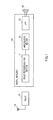
- a conventional digital amplifier apparatus 10 of this type (hereinafter simply referred to as a “digital amplifier”) is configured with a pulse width modulation section 11, an amplification section 12 and a lowpass filter (hereinafter abbreviated as "LPF") 13.
- LPF lowpass filter
- the pulse width modulation section 11 modulates an input signal from a tuner 15 connected to an antenna 14 by a pulse width modulation scheme.
- the amplification section 12 amplifies by switching operation the output signal subjected to pulse width modulation in the pulse width modulation section 11.
- the LPF 13 removes the high frequencies produced by the switching operation, and outputs the output signal to a speaker 16 connected to the digital amplifier apparatus 10.
- switching noise noise
- Patent Document 1 Japanese Patent Application Laid-Open No. 2004-363771
- the digital amplifier of the present invention amplifies an input signal from a tuner receiving a broadcast signal of a set receiving frequency, and employs a configuration having: a band division section that divides the input signal into a plurality of bands; a pulse width modulation section that modulates the bands of the input signal divided in the band division section by a pulse width modulation scheme; a switching frequency control section that acquires the receiving frequency in the tuner and controls switching frequencies in the pulse width modulation section; and an amplification section that amplifies the input signal subjected to pulse width modulation in the pulse width modulation section.
- the present invention it is possible to divide an input signal into a lower band and a higher band, and, during tuner operation, set a switching frequency low enough not to influence the receiving frequency with respect to the lower band part of the input signal, and set a switching frequency high enough not to influence the receiving frequency with respect to the higher band part of the input signal.
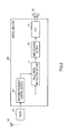
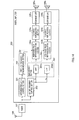
- FIG.3 is a block diagram showing an internal configuration of a digital amplifier according to Embodiment 1 of the present invention, and its peripheral configurations.
- a tuner 107 connected to an antenna 106, a high-band playback speaker 108a and a low-band playback speaker 108b are connected to a digital amplifier 100 of the present embodiment.
- the tuner 107 receives, for example, the broadcast wave of a channel (frequency) specified by the user through the antenna 106, and outputs the demodulated signal of the received signal and information indicating the current receiving frequency fo (hereinafter simply referred to as "receiving frequency information"), to the digital amplifier 100.
- the digital amplifier 100 of the present embodiment is provided with a switching frequency control section 101, a band division section 102, a high-band pulse width modulation section 103a, a low-band pulse width modulation section 103b, a high-band amplification section 104a, a low-band amplification section 104b, a high-band LPF 105a and a low-band LPF 105b.
- the switching frequency control section 101 determines a switching frequency fsa for the higher band and a switching frequency fsb for the lower band, based on receiving frequency information from the tuner 107, and reports these determined frequencies to the high-band pulse width modulation section 103a and the low-band pulse width modulation section 103b.
- the processing in this switching frequency control section 101 will be later described in detail with reference to FIG.4 .
- the band division section 102 includes a highpass filter (hereinafter abbreviated as "HPF") 102a that allows to pass higher frequency components of the output signal from the tuner 107 and an LPF 102b that allows to pass lower frequency component of the output signal from the tuner 107.
- HPF highpass filter
- the high-band pulse width modulation section 103a operates in the switching frequency fsa for the higher band specified by the switching frequency control section 101, and performs pulse width modulation of the output signal of the HPF 102a in the band division section 102.
- the high-band amplification section 104a performs class D amplification of the output signal of the high-band pulse width modulation section 103a.
- the high-band LPF 105a allows to pass lower frequency components included in the output signal of the high-band amplification section 104a, to remove the high frequencies produced by the switching operation.
- the output signal of the high-band LPF 105a is outputted to a high-band playback speaker 108a.
- the high-band playback speaker 108a outputs high-frequency sounds based on the input signal.
- the low-band pulse width modulation section 103b operates in the switching frequency fsb for the lower band specified by the switching frequency control section 101, and performs pulse width modulation of the output signal of the LPF 102b in the band division section 102.
- the low-band amplification section 104b performs class D amplification of the output signal of the low-band pulse width modulation section 103b.
- the low-band LPF 105b allows to pass lower frequency components included in the output signal of the low-band amplification section 104b, to remove the high frequencies produced by switching operation.
- the output signal of the low-band LPF 105b is outputted to a low-band playback speaker 108b.
- the low-band playback speaker 108b outputs low-frequency sounds based on the input signal.
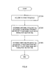
- the switching frequency control section 101 acquires receiving frequency information from the tuner 107 (step ST201).
- the switching frequency control section 101 determines a switching frequency fsa for the higher band that is high enough not to influence the receiving frequency in the tuner 107, and reports the determined switching frequency fsa for the higher band to the high-band pulse width modulation section 103a (step ST202).
- the switching frequency control section 101 determines a switching frequency fsb for the lower band that is low enough not to influence the receiving frequency in the tuner 107, and reports the determined switching frequency fsb for the lower band to the low-band pulse width modulation section 103b (step ST203).
- the switching frequency fsa for the higher band and the switching frequency fsb for the lower band that do not influence the receiving frequency refer to such frequencies that these frequencies fsa and fsb and the frequencies of their m/n multiples (where n and m are integers) do not overlap with the current receiving frequency fo and the beat noise produced by these frequencies fsa and fsb and the frequencies of their m/n multiples do not influence the audio band (i.e. 20 Hz to 20 kHz).
- the switching frequency fsa for the higher band is set to 384 kHz and the switching frequency fsb for the lower band is set to 96 kHz, which is lower than the receiving frequency fo.
- Combinations of the switching frequency fsa for the higher band and the switching frequency fsb for the lower band, whereby influence upon the tuner 107 can be suppressed, are determined in advance in accordance with the receiving frequency fo.
- the switching frequency control section 101 stores a table T, in which the receiving frequency fo and combinations of the switching frequency fsa for the higher band and the switching frequency fsb for the lower band are linked in one-to-one associations.
- the switching frequency control section 101 selects, in step ST202 and step ST203 in FIG.4 , the combination of a switching frequency fsa for the higher band and the switching frequency fsb for the lower band associated with the receiving frequency fo indicated by receiving frequency information from the tuner 107, and reports the switching frequency fsa and the switching frequency fsb to the high-band pulse width modulation section 103a and the low-band pulse width modulation section 103b.
- a received signal in the tuner 107 is divided into higher frequency components and lower frequency components, through the HPF 102a and the LPF 102b in the band division section 102.
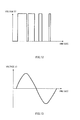
- the high-band pulse width modulation section 103a performs pulse width modulation of the higher frequency signal (see FIG.6 ) divided by the HPF 102a in the band division section 102, using the switching frequency fsa determined in the switching frequency control section 101.
- the high-band amplification section 104a amplifies, by switching operation, the output signal subjected to pulse width modulation in the high-band pulse width modulation section 103a (see FIG.7 ).
- the high-band LPF 105a removes the high frequencies produced by the switching operation, from the signal amplified in the high-band amplification section 104a (see FIG.8 ), demodulates the signal, and outputs the demodulated signal (see FIG.9 ) to the high-band playback speaker 108a.
- the low-band pulse width modulation section 103b performs pulse width modulation of the lower frequency signal (see FIG.10 ) divided by the LPF 102b in the band division section 102, using the switching frequency fsb determined in the switching frequency control section 101, which is different from the switching frequency fsa.
- the low-band amplification section 104b amplifies, by switching operation, the output signal subjected to pulse width modulation in the low-band pulse width modulation section 103b (see FIG.11 ).
- the low-band LPF 105b removes the high frequencies produced by the switching operation, from the signal amplified in the low-band amplification section 104b (see FIG.12 ), demodulates the signal, and outputs the demodulated signal (see FIG.13 ) to the low-band playback speaker 108b.
- switching is performed at a switching frequency fsa that is high enough not to influence the receiving frequency fo in the tuner 107, to suppress deterioration of playback performance, and, as for the lower band, switching is performed at a switching frequency fsb that is low enough not to influence the receiving frequency fo, to improve the efficiency of amplification.
- the received signal is divided in the band division section 102 into two, that is, into the higher band and the lower band, it is equally possible to divide the band into three or more in the band division section 102.
- the switching frequency control section 101 determines the switching frequency fsa and the switching frequency fsb using the table T shown in FIG.5 .
- the switching frequency control section 101 may equally make the receiving frequency fo a variable, store equations for finding the switching frequency fsa and the switching frequency fsb, and, upon receiving frequency information from the tuner 107, substitute the receiving frequency fo in these equations and find the switching frequency fsa and the switching frequency fsb.
- FIG.14 is a block diagram showing an internal configuration of a digital amplifier according to Embodiment 2 of the present invention and its peripheral configurations.
- a digital amplifier 200 of the present embodiment is unique in having a switching frequency control section 201 instead of the switching frequency control section 101 and having a HPF 202a and a LPF 202b in a band division section 202 instead of the HPF 102a and the LPF 102b in the band division section 102.
- the digital amplifier 200 of the present embodiment is unique in additionally having a cutoff frequency control section 203 and a switching frequency synchronization section 204.
- the high-band pulse width modulation section 103a and the low-band pulse width modulation section 103b, the high-band amplification section 104a and the low-band amplification section 104b, the high-band LPF 105a and the low-band LPF 105b of the digital amplifier 200 of the present embodiment and the digital amplifier 100 according to Embodiment 1 have the same processing functions, respectively, and therefore their explanations will be omitted.
- the switching frequency control section 201 determines a switching frequency fsa for the higher band and a switching frequency fsc for the lower band, based on the receiving frequency from the tuner 107, and gives the determined frequencies to a switching frequency synchronization section 204.
- the processing in this switching frequency control section 201 will be later described in detail with reference to FIG.15 .
- the HPF 202a in the band division section 202 allows to pass frequency bands equal to or higher than the cutoff frequency fc set in the cutoff frequency control section 203.
- the LPF 202b in the band division section 202 allows to pass frequency bands equal to or lower than the cutoff frequency fc set in the cutoff frequency control section 203.
- the cutoff frequency control section 203 determines the cutoff frequency fc and sets the determined cutoff frequency fc in the HPF 202a and the LPF 202b in the band division section 202, respectively.
- the switching frequency synchronization section 204 sets the switching frequency fsa for the higher band determined in the switching frequency control section 201 in the high-band pulse width modulation section 103a, and sets the switching frequency fsc for the lower band determined in the switching frequency control section 201 in the low-band pulse width modulation section 103b.
- the switching frequency synchronization section 204 establishes switching synchronization between the high-band pulse width modulation section 103a and the low-band pulse width modulation section 103b.
- the switching frequency control section 201 and the cutoff frequency control section 203 acquire receiving frequency information from the tuner 107 (step ST1301).
- the cutoff frequency control section 203 determines the cutoff frequency fc and sets the determined cutoff frequency fc in the HPF 202a and the LPF 202b (step ST1302).
- the switching frequency control section 201 determines a switching frequency fsa for the higher band that is high enough not to influence the receiving frequency in the tuner 107.
- the switching frequency fsa determined in the switching frequency control section 201 is sent to the switching frequency synchronization section 204 and reported to the high-band pulse width modulation section 103a (step ST1303).
- the switching frequency control section 201 determines a switching frequency fsc that is low enough not to influence the receiving frequency in the tuner 107.
- the switching frequency fsc determined here is an integer fraction of the switching frequency fsa, in order to acquire synchronization between the high-band pulse width modulation section 103a and the low-band pulse width modulation section 103b.
- the switching frequency fsc determined this way is sent to the switching frequency synchronization section 204 and reported to the low-band pulse width modulation section 103b (step ST1304).
- the switching frequency fsc for the lower band is preferably 50 kHz or less, taking into account the influence up to the twentieth order harmonic. If the frequency of an eighth of the switching frequency fsc is a speech band that can be modulated without damaging sound quality, it is possible to make the cutoff frequency fc 6.25 kHz. Furthermore, if the receiving frequency fo is 600 kHz, the cutoff frequency fc becomes 3.75 kHz.
- the switching frequencies fsa and fsc may be determined with reference to a table T that is provided in advance, as in the case of the switching frequency control section 101 in the digital amplifier 100 according to Embodiment 1, or may be determined using equations defined in advance.
- this digital amplifier 200 establishes switching synchronization by the switching frequency synchronization section 204, so that it is possible to prevent switching noise interference between the higher band and the lower band from producing beat and providing noise in the audible band.
- the received signal is divided in the band division section 202 into the higher band and the lower band, that is, where the band is divided into two, it is equally possible to divide the band into three or more.
- cutoff frequency control section 203 determines a single cutoff frequency fc, this is by no means limiting, and it is equally possible to determine a plurality of varying cutoff frequencies between the HPF 202a and the LPF 202b.
- the digital amplifier apparatus can suppress the deterioration of high-band playback performance and a decrease in amplification efficiency, and is therefore suitable for use as a digital amplifier apparatus that performs amplification by a class D amplification scheme.
Landscapes
- Engineering & Computer Science (AREA)
- Power Engineering (AREA)
- Amplifiers (AREA)
- Noise Elimination (AREA)
Applications Claiming Priority (2)
| Application Number | Priority Date | Filing Date | Title |
|---|---|---|---|
| JP2006232442A JP5096710B2 (ja) | 2006-08-29 | 2006-08-29 | デジタルアンプ装置 |
| PCT/JP2007/066661 WO2008026585A1 (en) | 2006-08-29 | 2007-08-28 | Digital amplifier |
Publications (3)
| Publication Number | Publication Date |
|---|---|
| EP2058942A1 true EP2058942A1 (de) | 2009-05-13 |
| EP2058942A4 EP2058942A4 (de) | 2012-01-25 |
| EP2058942B1 EP2058942B1 (de) | 2017-05-31 |
Family
ID=39135868
Family Applications (1)
| Application Number | Title | Priority Date | Filing Date |
|---|---|---|---|
| EP07806140.5A Not-in-force EP2058942B1 (de) | 2006-08-29 | 2007-08-28 | Digitaler verstärker |
Country Status (5)
| Country | Link |
|---|---|
| US (1) | US8189655B2 (de) |
| EP (1) | EP2058942B1 (de) |
| JP (1) | JP5096710B2 (de) |
| CN (1) | CN101512896B (de) |
| WO (1) | WO2008026585A1 (de) |
Families Citing this family (7)
| Publication number | Priority date | Publication date | Assignee | Title |
|---|---|---|---|---|
| US8391512B2 (en) * | 2009-09-25 | 2013-03-05 | Onkyo Corporation | Broadcast wave receiving system |
| US10504132B2 (en) | 2012-11-27 | 2019-12-10 | American Express Travel Related Services Company, Inc. | Dynamic rewards program |
| KR101588697B1 (ko) * | 2014-01-20 | 2016-01-28 | 주식회사 솔루엠 | 방송 신호 수신장치 |
| CN105910713B (zh) * | 2016-04-11 | 2018-12-07 | 杭州富阳鼎创科技有限公司 | 一种基于plc的温度信号采集系统 |
| CN105790721B (zh) * | 2016-04-11 | 2018-11-09 | 深圳供电局有限公司 | 一种温度信号处理装置 |
| CN105763625B (zh) * | 2016-04-11 | 2019-02-15 | 宁夏嘉友信通信息技术有限公司 | 一种温度信息采集系统 |
| CN105890772B (zh) * | 2016-04-11 | 2019-03-22 | 镇雄易和互联有限公司 | 一种远程温度信息报警系统 |
Family Cites Families (14)
| Publication number | Priority date | Publication date | Assignee | Title |
|---|---|---|---|---|
| JPH09260976A (ja) * | 1996-03-19 | 1997-10-03 | Nec Corp | 電界効果トランジスタ増幅器 |
| JPH09260967A (ja) | 1996-03-26 | 1997-10-03 | Aiwa Co Ltd | 電子機器 |
| JPH11274863A (ja) * | 1998-03-24 | 1999-10-08 | Sony Corp | スイッチング増幅器 |
| US6587670B1 (en) | 1998-12-22 | 2003-07-01 | Harris Corporation | Dual mode class D amplifiers |
| US6549616B1 (en) * | 2000-03-20 | 2003-04-15 | Serconet Ltd. | Telephone outlet for implementing a local area network over telephone lines and a local area network using such outlets |
| US6605991B2 (en) | 2001-08-30 | 2003-08-12 | Motorola, Inc. | Circuitry for creating a spectral null in a differential output switching amplifier and method therefor |
| US6819912B2 (en) * | 2001-11-05 | 2004-11-16 | Freescale Semiconductor, Inc. | Variable frequency switching amplifier and method therefor |
| JP2004048701A (ja) * | 2002-05-14 | 2004-02-12 | Sony Corp | オーディオ装置及びオーディオ装置の制御方法 |
| US7110737B2 (en) | 2002-05-14 | 2006-09-19 | Sony Corporation | Audio equipment and control method of audio equipment |
| JP2004048333A (ja) * | 2002-07-11 | 2004-02-12 | Victor Co Of Japan Ltd | Pwm変調方式d級アンプ |
| JP4197988B2 (ja) | 2003-06-03 | 2008-12-17 | シャープ株式会社 | オーディオ再生装置 |
| JP2005051289A (ja) * | 2003-07-29 | 2005-02-24 | Pioneer Electronic Corp | 多チャンネルデジタルアンプ装置 |
| JP2006121425A (ja) * | 2004-10-21 | 2006-05-11 | Pioneer Electronic Corp | D級増幅装置 |
| JP2006232442A (ja) | 2005-02-23 | 2006-09-07 | Canon Inc | シート搬送装置及び該装置を備えた画像形成装置 |
-
2006
- 2006-08-29 JP JP2006232442A patent/JP5096710B2/ja not_active Expired - Fee Related
-
2007
- 2007-08-28 EP EP07806140.5A patent/EP2058942B1/de not_active Not-in-force
- 2007-08-28 CN CN2007800321797A patent/CN101512896B/zh not_active Expired - Fee Related
- 2007-08-28 US US12/439,124 patent/US8189655B2/en active Active
- 2007-08-28 WO PCT/JP2007/066661 patent/WO2008026585A1/ja not_active Ceased
Also Published As
| Publication number | Publication date |
|---|---|
| US8189655B2 (en) | 2012-05-29 |
| WO2008026585A1 (en) | 2008-03-06 |
| CN101512896B (zh) | 2012-09-26 |
| US20100014574A1 (en) | 2010-01-21 |
| EP2058942A4 (de) | 2012-01-25 |
| CN101512896A (zh) | 2009-08-19 |
| EP2058942B1 (de) | 2017-05-31 |
| JP2008060705A (ja) | 2008-03-13 |
| JP5096710B2 (ja) | 2012-12-12 |
Similar Documents
| Publication | Publication Date | Title |
|---|---|---|
| US8189655B2 (en) | Digital amplifier | |
| JP5488389B2 (ja) | 音響信号処理装置 | |
| US8600076B2 (en) | Multiband DRC system and method for controlling the same | |
| EP1542359B1 (de) | Gerät zur Dynamikbegrenzung/-dehnung und mobiles Kommunikationsgerät | |
| DK2244491T4 (en) | A method of operating a hearing device and the hearing aid with a frekvensomskifter | |
| US10742187B2 (en) | System and method for distortion limiting | |
| KR100554066B1 (ko) | 가변 평균 스위칭 주파수를 갖는 펄스폭 변조 방식 오디오증폭기 | |
| US9473102B2 (en) | Level adjusting circuit, digital sound processor, audio AMP integrated circuit, electronic apparatus and method of automatically adjusting level of audio signal | |
| KR102837086B1 (ko) | 클리핑 일그러짐을 방지하거나 액티브 스피커의 최대 사운드 레벨을 높이기 위한 제한기 시스템 및 방법 | |
| JP3914743B2 (ja) | ノイズ減少及び音質が改善された分割バンド可聴周波数圧縮/伸張システムを有する無線マイクロホン | |
| US11563425B2 (en) | Linear-phase fir audio filter, production method and signal processor | |
| KR20050036812A (ko) | 오디오 신호에 대한 음질 개선 회로 및 이를 이용한오디오 증폭 회로 | |
| JP4893189B2 (ja) | Fmチューナ | |
| JP2004312077A (ja) | Fmチューナ | |
| JPH08316760A (ja) | 音声信号制限増幅装置 | |
| JPWO2006049154A1 (ja) | デジタルアンプ装置 | |
| KR101704048B1 (ko) | 음향시스템 및 그 제어 방법 | |
| JP2002009650A (ja) | Fm受信機 | |
| JP2709855B2 (ja) | スピーカー駆動回路 | |
| JP2005143093A (ja) | オーディオ信号の音質改善回路およびこれを用いるオーディオ増幅回路 | |
| JPH05266582A (ja) | 音響装置 | |
| JP2004221748A (ja) | 音響信号増幅装置 | |
| JP2006013600A (ja) | 高周波増幅装置 | |
| KR20040058696A (ko) | 휴대용 단말기 벨음질 향상 장치 | |
| JPH09298432A (ja) | Cw受信音質補償方式 |
Legal Events
| Date | Code | Title | Description |
|---|---|---|---|
| PUAI | Public reference made under article 153(3) epc to a published international application that has entered the european phase |
Free format text: ORIGINAL CODE: 0009012 |
|
| 17P | Request for examination filed |
Effective date: 20090227 |
|
| AK | Designated contracting states |
Kind code of ref document: A1 Designated state(s): AT BE BG CH CY CZ DE DK EE ES FI FR GB GR HU IE IS IT LI LT LU LV MC MT NL PL PT RO SE SI SK TR |
|
| AX | Request for extension of the european patent |
Extension state: AL BA HR MK RS |
|
| DAX | Request for extension of the european patent (deleted) | ||
| RBV | Designated contracting states (corrected) |
Designated state(s): DE FR GB |
|
| A4 | Supplementary search report drawn up and despatched |
Effective date: 20111229 |
|
| RIC1 | Information provided on ipc code assigned before grant |
Ipc: H03F 3/217 20060101AFI20111222BHEP |
|
| RAP1 | Party data changed (applicant data changed or rights of an application transferred) |
Owner name: PANASONIC INTELLECTUAL PROPERTY MANAGEMENT CO., LT |
|
| RAP1 | Party data changed (applicant data changed or rights of an application transferred) |
Owner name: PANASONIC INTELLECTUAL PROPERTY MANAGEMENT CO., LT |
|
| GRAP | Despatch of communication of intention to grant a patent |
Free format text: ORIGINAL CODE: EPIDOSNIGR1 |
|
| STAA | Information on the status of an ep patent application or granted ep patent |
Free format text: STATUS: GRANT OF PATENT IS INTENDED |
|
| INTG | Intention to grant announced |
Effective date: 20161215 |
|
| RIN1 | Information on inventor provided before grant (corrected) |
Inventor name: HOMMA, RYOTA Inventor name: KUDO, KOJI |
|
| GRAS | Grant fee paid |
Free format text: ORIGINAL CODE: EPIDOSNIGR3 |
|
| GRAA | (expected) grant |
Free format text: ORIGINAL CODE: 0009210 |
|
| STAA | Information on the status of an ep patent application or granted ep patent |
Free format text: STATUS: THE PATENT HAS BEEN GRANTED |
|
| AK | Designated contracting states |
Kind code of ref document: B1 Designated state(s): DE FR GB |
|
| REG | Reference to a national code |
Ref country code: GB Ref legal event code: FG4D |
|
| REG | Reference to a national code |
Ref country code: DE Ref legal event code: R096 Ref document number: 602007051179 Country of ref document: DE |
|
| REG | Reference to a national code |
Ref country code: DE Ref legal event code: R097 Ref document number: 602007051179 Country of ref document: DE |
|
| PLBE | No opposition filed within time limit |
Free format text: ORIGINAL CODE: 0009261 |
|
| STAA | Information on the status of an ep patent application or granted ep patent |
Free format text: STATUS: NO OPPOSITION FILED WITHIN TIME LIMIT |
|
| GBPC | Gb: european patent ceased through non-payment of renewal fee |
Effective date: 20170831 |
|
| 26N | No opposition filed |
Effective date: 20180301 |
|
| REG | Reference to a national code |
Ref country code: FR Ref legal event code: ST Effective date: 20180430 |
|
| PG25 | Lapsed in a contracting state [announced via postgrant information from national office to epo] |
Ref country code: GB Free format text: LAPSE BECAUSE OF NON-PAYMENT OF DUE FEES Effective date: 20170831 |
|
| PG25 | Lapsed in a contracting state [announced via postgrant information from national office to epo] |
Ref country code: FR Free format text: LAPSE BECAUSE OF NON-PAYMENT OF DUE FEES Effective date: 20170831 |
|
| REG | Reference to a national code |
Ref country code: DE Ref legal event code: R084 Ref document number: 602007051179 Country of ref document: DE |
|
| PGFP | Annual fee paid to national office [announced via postgrant information from national office to epo] |
Ref country code: DE Payment date: 20221215 Year of fee payment: 17 |
|
| REG | Reference to a national code |
Ref country code: DE Ref legal event code: R119 Ref document number: 602007051179 Country of ref document: DE |
|
| PG25 | Lapsed in a contracting state [announced via postgrant information from national office to epo] |
Ref country code: DE Free format text: LAPSE BECAUSE OF NON-PAYMENT OF DUE FEES Effective date: 20250301 |