EP2078694A2 - Système de protection et procédé d'individualisation de structures MEMS - Google Patents
Système de protection et procédé d'individualisation de structures MEMS Download PDFInfo
- Publication number
- EP2078694A2 EP2078694A2 EP20080105987 EP08105987A EP2078694A2 EP 2078694 A2 EP2078694 A2 EP 2078694A2 EP 20080105987 EP20080105987 EP 20080105987 EP 08105987 A EP08105987 A EP 08105987A EP 2078694 A2 EP2078694 A2 EP 2078694A2
- Authority
- EP
- European Patent Office
- Prior art keywords
- protective layer
- protection system
- fragile
- layer
- structures
- Prior art date
- Legal status (The legal status is an assumption and is not a legal conclusion. Google has not performed a legal analysis and makes no representation as to the accuracy of the status listed.)
- Withdrawn
Links
- 238000000034 method Methods 0.000 title claims abstract description 42
- 239000011241 protective layer Substances 0.000 claims abstract description 30
- 239000010410 layer Substances 0.000 claims abstract description 27
- 229920000642 polymer Polymers 0.000 claims abstract description 17
- 239000012528 membrane Substances 0.000 claims abstract description 15
- 230000005855 radiation Effects 0.000 claims abstract description 5
- 229920000515 polycarbonate Polymers 0.000 claims abstract description 3
- 239000004417 polycarbonate Substances 0.000 claims abstract description 3
- 239000011888 foil Substances 0.000 claims description 14
- 238000004519 manufacturing process Methods 0.000 claims description 11
- 238000005530 etching Methods 0.000 claims description 9
- 229910000577 Silicon-germanium Inorganic materials 0.000 claims description 6
- 239000007788 liquid Substances 0.000 claims description 4
- 238000004528 spin coating Methods 0.000 claims description 3
- FGUUSXIOTUKUDN-IBGZPJMESA-N C1(=CC=CC=C1)N1C2=C(NC([C@H](C1)NC=1OC(=NN=1)C1=CC=CC=C1)=O)C=CC=C2 Chemical compound C1(=CC=CC=C1)N1C2=C(NC([C@H](C1)NC=1OC(=NN=1)C1=CC=CC=C1)=O)C=CC=C2 FGUUSXIOTUKUDN-IBGZPJMESA-N 0.000 claims description 2
- 229920000636 poly(norbornene) polymer Polymers 0.000 abstract description 2
- 239000011248 coating agent Substances 0.000 abstract 1
- 238000000576 coating method Methods 0.000 abstract 1
- 235000012431 wafers Nutrition 0.000 description 13
- XLYOFNOQVPJJNP-UHFFFAOYSA-N water Substances O XLYOFNOQVPJJNP-UHFFFAOYSA-N 0.000 description 11
- 238000000926 separation method Methods 0.000 description 7
- 238000000354 decomposition reaction Methods 0.000 description 5
- 230000001681 protective effect Effects 0.000 description 5
- XUIMIQQOPSSXEZ-UHFFFAOYSA-N Silicon Chemical compound [Si] XUIMIQQOPSSXEZ-UHFFFAOYSA-N 0.000 description 4
- 229910052710 silicon Inorganic materials 0.000 description 4
- 239000010703 silicon Substances 0.000 description 4
- 239000002131 composite material Substances 0.000 description 3
- 239000000463 material Substances 0.000 description 3
- 238000003698 laser cutting Methods 0.000 description 2
- 230000001133 acceleration Effects 0.000 description 1
- 238000009825 accumulation Methods 0.000 description 1
- 238000009529 body temperature measurement Methods 0.000 description 1
- 238000004140 cleaning Methods 0.000 description 1
- 238000001816 cooling Methods 0.000 description 1
- 230000010354 integration Effects 0.000 description 1
- 238000010030 laminating Methods 0.000 description 1
- 238000001459 lithography Methods 0.000 description 1
- 238000005259 measurement Methods 0.000 description 1
- 238000004377 microelectronic Methods 0.000 description 1
- 238000000059 patterning Methods 0.000 description 1
- 230000035515 penetration Effects 0.000 description 1
- 229920002120 photoresistant polymer Polymers 0.000 description 1
- 238000001020 plasma etching Methods 0.000 description 1
- 239000000126 substance Substances 0.000 description 1
- 239000000758 substrate Substances 0.000 description 1
- 210000002105 tongue Anatomy 0.000 description 1
Images


Classifications
-
- B—PERFORMING OPERATIONS; TRANSPORTING
- B81—MICROSTRUCTURAL TECHNOLOGY
- B81C—PROCESSES OR APPARATUS SPECIALLY ADAPTED FOR THE MANUFACTURE OR TREATMENT OF MICROSTRUCTURAL DEVICES OR SYSTEMS
- B81C1/00—Manufacture or treatment of devices or systems in or on a substrate
- B81C1/00865—Multistep processes for the separation of wafers into individual elements
- B81C1/00896—Temporary protection during separation into individual elements
-
- B—PERFORMING OPERATIONS; TRANSPORTING
- B81—MICROSTRUCTURAL TECHNOLOGY
- B81B—MICROSTRUCTURAL DEVICES OR SYSTEMS, e.g. MICROMECHANICAL DEVICES
- B81B2201/00—Specific applications of microelectromechanical systems
- B81B2201/02—Sensors
- B81B2201/0257—Microphones or microspeakers
-
- B—PERFORMING OPERATIONS; TRANSPORTING
- B81—MICROSTRUCTURAL TECHNOLOGY
- B81C—PROCESSES OR APPARATUS SPECIALLY ADAPTED FOR THE MANUFACTURE OR TREATMENT OF MICROSTRUCTURAL DEVICES OR SYSTEMS
- B81C2201/00—Manufacture or treatment of microstructural devices or systems
- B81C2201/05—Temporary protection of devices or parts of the devices during manufacturing
- B81C2201/053—Depositing a protective layers
Definitions
- the invention relates to a protection system for singling MEMS structures, and to a method by means of which the singulation of fragile open sensors, in particular in micromechanical components, can be simplified.
- Micromechanical structures are manufactured using microtechnology methods and have high precision. They either serve as holding structures for receiving miniaturized components or are realized as movable elements, for example in the form of tongues or fingers, oscillating structures, or micromotors, by means of bulk or surface micromechanics.
- micromechanical systems that are industrially manufactured are: acceleration sensors, yaw rate sensors, electrostatic and electromagnetic linear actuators (microactuators), micromotors, gears for microgear, capacitive microphones, gripper structures, bimorph structures for temperature measurement or piezoelectric layer structures for strain or voltage measurement.
- micromechanical structures can be fabricated together with the microelectronic circuit on a substrate. Such an integrated structure reduces manufacturing costs and reduces the susceptibility to interference.
- the step of separating the MEMS structures fabricated by patterning in a contiguous series plays a major role. In general, the separation is currently done by sawing with a water-cooled circular saw.
- the protection system for MEMS structures comprises a fragile open structure and an optional sacrificial layer applied to a wafer, wherein a protective layer is applied to the front side of the structure, which can be removed without residue.
- open fragile structure is understood as meaning both membranes and comb structures, finger structures, beam structures and similar structures, a membrane being particularly preferred as an open, fragile structure. They may preferably be made of silicon according to the invention, but other suitable materials are equally possible.
- the first time it is possible for the first time to apply a protective layer to MEMS structures, which can be removed again after the production process and in particular after the separation step without residues.
- the protective layer also achieves mechanical protection of the structures in front of the pending water jet and during the intermediate process steps. Even with non-water-assisted separation processes, all of which are material-removing, such as laser cutting, for example, protection of the fragile structures from the accumulation of material with the protective layer can be achieved.
- This can be the first time
- Protective system can be made available that allows only the use of established in micromechanical series processes with conventional systems for fragile, open MEMS structures.
- protection system according to the invention in comparison to the known protective caps made of silicon is significantly cheaper to manufacture and processing and also allows a simplified application to the fragile structures.
- Complex film processes for protecting the micromechanical component, for example in the case of sensitive membranes, can also be dispensed with.
- the protective layer comprises a polymer which is thermally and / or by means of radiation decomposable.
- a plasma process can also be used.
- polynorbornene or polycarbonate can be used as decomposable polymers.
- those polymers are selected whose decomposition temperature is compatible with the IC components, whereby a good integration capability is ensured.
- plasma etching steps or lithography processes can be carried out in the context of the method according to the invention.
- the protective layer can preferably be applied by spin-coating a liquid, thermally and / or radiation-decomposable polymer, it also being possible to use a plasma process as a special form of the radiation for decomposition.
- the protective layer at temperatures between 80 ° C and 450 ° C, preferably at temperatures between 100 ° C and 250 ° C, are removed without residue.
- the decomposition can be supported by irradiation, for example with UV light, so that a decomposition temperature of about 100 ° C can be achieved.
- the sawing foil which is located on the back of the sensor, not damaged, so that they can continue to serve as a carrier for the now isolated MEMS structures.
- deep trench and / or oxide opening can be carried out as plasma backside processes.
- the sacrificial layer may be a SiGe or oxide layer and the SiGe layer may be etched with CLF 3 gas and the oxide layer etched with HF vapor.
- the protective layer can advantageously ensure chemical and mechanical protection for the fragile structure in all of these process steps and stabilize the structure.
- the sawing foil can be expanded following step f).
- the distance between the now separated components is increased and the individual structures can be picked and packaged from the film, for example with pick-and-place tools.
- a protection system according to the invention for the production of micromechanical components with fragile open MEMS structures, in particular for the production of capacitive microphones, is used.
- Fig. 1 shows in a schematic cross-sectional view of the protection system according to the invention the initial state for the production of fragile, open MEMS structures.
- the residue-free removable protective layer 10 is applied directly to the front of the fragile, open structure 12.
- the example of a membrane sensor shown here further comprises an optional sacrificial layer 13, for example made of an oxide or of SiGe, which is placed between the membrane 12 and the wafer 14.
- the residue-free decomposable polymer used as protective layer 10 is applied to the fragile structures 12 for protection. This is done in the case of the capacitive microphone in a process state in which the component front and back is still completely closed and has no trenches or holes.
- the polymer is applied to the membrane 12, which is still stabilized by the sacrificial layer 13 at this time, on the front side of the sensor.
- This can preferably be done by spin-coating the liquid Polymers take place, as used for example for the application of photoresists on wafers in micromechanics.
- the polymer when it is applied, it can not pass through the openings of the membrane into the gap between the two electrodes, since the sacrificial layer is still present in the sensor at this time.
- Fig. 2 shows a schematic cross-sectional view of the protection system according to the invention Fig. 1 after completion of the backside processes.
- suitable backside processes are deep trench etching and oxide opening, which are described, inter alia, in US Pat DE 10 2005 004 877 A1 and the DE 42 41 045 C2 described in more detail and are known in the art.
- Fig. 3 shows a schematic cross-sectional view of the protection system according to the invention Fig. 2 after sacrificial layer etching.
- the sacrificial layer process exposes the membrane 12.
- etching may be employed with, for example, ClF 3 gas in the case of a sacrificial SiGe layer or RF vapor in the case of a sacrificial sacrificial layer.
- ClF 3 gas in the case of a sacrificial SiGe layer
- RF vapor in the case of a sacrificial sacrificial layer.
- the component has now undergone all manufacturing processes that take place at the wafer level.
- the membrane 12 is covered only with the polymeric protective layer 10, which is removed only in the isolated state.
- Fig. 4 Therefore, shows a schematic cross-sectional view of the protection system of the invention Fig. 3 as composite after performing the sacrificial layer etching.
- Fig. 5 shows a schematic cross-sectional view of the protection system according to the invention Fig. 4 after application of the sawing foil 15 on the sensor back.
- the membrane 12 is protected and stabilized by the protective layer 10.
- Fig. 6 shows a schematic cross-sectional view of the protection system according to the invention Fig. 5 after completion of the separation.
- the singling can preferably be done by sawing from the front.
- another materialbatforming separation for example by means of laser cutting, possible.
- the membrane 12 is protected during the sawing process by the protective layer 10 from water penetration and from the mechanical water pressure of the jet.
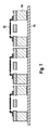
- Fig. 7 shows a schematic cross-sectional view of the protection system according to the invention Fig. 6 after residue-free removal of the protective layer 10.
- the composite of individual wafers 14 with the sawing foil 15 and the polymer protective layer 10 after sawing can be heated and / or irradiated in such a way that the polymer decomposes completely and without residue.
- the decomposition typically occurs at temperatures around 200 ° C.
- the sawn wafer 14 can be exposed to the polymer layer on the sawing foil 15.
- the polymers then decompose even at significantly lower temperatures by about 100 ° C.
- the sawing foil 15 is not damaged.
- the sawing foil 15 can, for example, first be expanded so that the individual structures are arranged at a greater distance. This simplifies the subsequent picking of the sawing foil 15, which can be carried out, for example, with pick-and-place tools.
- the individual structures can be finally packed and further processed.
Landscapes
- Engineering & Computer Science (AREA)
- Manufacturing & Machinery (AREA)
- Microelectronics & Electronic Packaging (AREA)
- Micromachines (AREA)
- Dicing (AREA)
Applications Claiming Priority (1)
| Application Number | Priority Date | Filing Date | Title |
|---|---|---|---|
| DE200810003452 DE102008003452A1 (de) | 2008-01-08 | 2008-01-08 | Schutzsystem und Verfahren zur Vereinzelung von MEMS-Strukturen |
Publications (2)
| Publication Number | Publication Date |
|---|---|
| EP2078694A2 true EP2078694A2 (fr) | 2009-07-15 |
| EP2078694A3 EP2078694A3 (fr) | 2013-06-26 |
Family
ID=40379762
Family Applications (1)
| Application Number | Title | Priority Date | Filing Date |
|---|---|---|---|
| EP08105987.5A Withdrawn EP2078694A3 (fr) | 2008-01-08 | 2008-12-16 | Système de protection et procédé d'individualisation de structures MEMS |
Country Status (3)
| Country | Link |
|---|---|
| EP (1) | EP2078694A3 (fr) |
| DE (1) | DE102008003452A1 (fr) |
| TW (1) | TWI469914B (fr) |
Cited By (1)
| Publication number | Priority date | Publication date | Assignee | Title |
|---|---|---|---|---|
| CN102209287A (zh) * | 2010-03-29 | 2011-10-05 | 歌尔声学股份有限公司 | Mems麦克风芯片及其制造方法 |
Families Citing this family (3)
| Publication number | Priority date | Publication date | Assignee | Title |
|---|---|---|---|---|
| DE102012203135B4 (de) * | 2012-02-29 | 2020-11-12 | Robert Bosch Gmbh | Mikromechanische Sensoranordnung und ein entsprechendes Herstellungsverfahren sowie entsprechende Verwendung |
| US9402138B2 (en) | 2012-10-12 | 2016-07-26 | Infineon Technologies Ag | MEMS device and method of manufacturing a MEMS device |
| CN103402162A (zh) * | 2013-07-23 | 2013-11-20 | 上海集成电路研发中心有限公司 | 具有凹凸结构振动膜的电容式硅麦克风及其制备方法 |
Citations (2)
| Publication number | Priority date | Publication date | Assignee | Title |
|---|---|---|---|---|
| DE4241045C1 (de) | 1992-12-05 | 1994-05-26 | Bosch Gmbh Robert | Verfahren zum anisotropen Ätzen von Silicium |
| DE102005004877A1 (de) | 2005-02-03 | 2006-08-10 | Robert Bosch Gmbh | Mikromechanisches Bauelement und entsprechendes Herstellungsverfahren |
Family Cites Families (7)
| Publication number | Priority date | Publication date | Assignee | Title |
|---|---|---|---|---|
| US6287885B1 (en) * | 1998-05-08 | 2001-09-11 | Denso Corporation | Method for manufacturing semiconductor dynamic quantity sensor |
| JP4150003B2 (ja) * | 2003-04-25 | 2008-09-17 | 富士通株式会社 | マイクロ構造体の製造方法およびマイクロ構造体 |
| US7422928B2 (en) * | 2003-09-22 | 2008-09-09 | Matsushita Electric Works, Ltd. | Process for fabricating a micro-electro-mechanical system with movable components |
| TW593126B (en) * | 2003-09-30 | 2004-06-21 | Prime View Int Co Ltd | A structure of a micro electro mechanical system and manufacturing the same |
| US7294279B2 (en) * | 2005-03-17 | 2007-11-13 | Taiwan Semiconductor Manufacturing Co., Ltd. | Method for releasing a micromechanical structure |
| TWI395258B (zh) * | 2005-11-11 | 2013-05-01 | Semiconductor Energy Lab | 微結構以及微機電系統的製造方法 |
| US7297567B2 (en) * | 2006-01-10 | 2007-11-20 | Knowles Electronics, Llc. | Method for singulating a released microelectromechanical system wafer |
-
2008
- 2008-01-08 DE DE200810003452 patent/DE102008003452A1/de not_active Withdrawn
- 2008-12-16 EP EP08105987.5A patent/EP2078694A3/fr not_active Withdrawn
-
2009
- 2009-01-06 TW TW98100130A patent/TWI469914B/zh not_active IP Right Cessation
Patent Citations (2)
| Publication number | Priority date | Publication date | Assignee | Title |
|---|---|---|---|---|
| DE4241045C1 (de) | 1992-12-05 | 1994-05-26 | Bosch Gmbh Robert | Verfahren zum anisotropen Ätzen von Silicium |
| DE102005004877A1 (de) | 2005-02-03 | 2006-08-10 | Robert Bosch Gmbh | Mikromechanisches Bauelement und entsprechendes Herstellungsverfahren |
Cited By (2)
| Publication number | Priority date | Publication date | Assignee | Title |
|---|---|---|---|---|
| CN102209287A (zh) * | 2010-03-29 | 2011-10-05 | 歌尔声学股份有限公司 | Mems麦克风芯片及其制造方法 |
| CN102209287B (zh) * | 2010-03-29 | 2014-10-15 | 歌尔声学股份有限公司 | Mems麦克风芯片及其制造方法 |
Also Published As
| Publication number | Publication date |
|---|---|
| TW200940438A (en) | 2009-10-01 |
| EP2078694A3 (fr) | 2013-06-26 |
| DE102008003452A1 (de) | 2009-07-09 |
| TWI469914B (zh) | 2015-01-21 |
Similar Documents
| Publication | Publication Date | Title |
|---|---|---|
| EP2282969B1 (fr) | Procédé pour produire des composants micromécaniques individuels placés sur un substrat de silicium et composants produits selon ce procédé | |
| EP2438767B1 (fr) | Élément avec une structure de microphone microméchanique et procédé pour produire un tel élément | |
| EP1866236B1 (fr) | Composant micromecanique, et son procede de production | |
| DE102011084020B4 (de) | Sensorelement | |
| DE102008005686B4 (de) | MEMS-Bauelement und Verfahren zur Herstellung eines MEMS-Bauelements | |
| DE102020101520B4 (de) | Halbleitervorrichtung und verfahren | |
| DE102020103732B4 (de) | Verfahren mit mechanischem Dicing-Prozess zur Herstellung von MEMS-Bauelementen | |
| EP2078694A2 (fr) | Système de protection et procédé d'individualisation de structures MEMS | |
| EP1997137B1 (fr) | Procédé pour produire un circuit intégré | |
| DE102011116988A1 (de) | Entfernbare Anordnung zur Kontrolle des Verbindungsabstands von Substraten | |
| DE102014202842B4 (de) | Verfahren zum Herstellen eines mikromechanischen Bauteils | |
| WO2003053844A1 (fr) | Procede et dispositif de fabrication d'un composant presentant une structure mobile | |
| DE102015213714B4 (de) | Mikromechanisches Bauteil und Verfahren zur Herstellung eines piezoelektrischen mikromechanischen Bauteils | |
| EP3201941B1 (fr) | Procédé combiné de fabrication de tranches au moyen d'une couche réceptrice pourvue de trous | |
| DE102009046461B4 (de) | Verfahren zur Herstellung verkappter mikroelektromechanischer Bauelemente | |
| EP3601154B1 (fr) | Procédé servant à fabriquer une tranche semi-conductrice au moins en partie encapsulée | |
| EP4537550B1 (fr) | Procédé de fabrication d'une pluralité de transducteurs mems à capacité élevée | |
| EP1663852B1 (fr) | Procédé d'individualisation de composants | |
| DE102023202714A1 (de) | Herstellung einer MEMS-basierten Vorrichtung unter Zuhilfenahme von temporären Schutzkappen | |
| DE102022201365A1 (de) | Wafer-Vereinzelungsfolie | |
| DE102023210603A1 (de) | Verfahren zum Verarbeiten eines Wafers | |
| DE102018219537A1 (de) | Verfahren zum Herstellen einer mikromechanischen Vorrichtung | |
| WO2025176544A1 (fr) | Procédé d'intégration et/ou de traitement d'au moins un substrat et empilement de substrats | |
| WO2024146713A1 (fr) | Procédé de production avec protection temporaire de microstructures | |
| DE102006022808A1 (de) | Verfahren zur Vereinzelung von insbesondere mikromechanischen Bauelementen und Bauelement |
Legal Events
| Date | Code | Title | Description |
|---|---|---|---|
| PUAI | Public reference made under article 153(3) epc to a published international application that has entered the european phase |
Free format text: ORIGINAL CODE: 0009012 |
|
| AK | Designated contracting states |
Kind code of ref document: A2 Designated state(s): AT BE BG CH CY CZ DE DK EE ES FI FR GB GR HR HU IE IS IT LI LT LU LV MC MT NL NO PL PT RO SE SI SK TR |
|
| AX | Request for extension of the european patent |
Extension state: AL BA MK RS |
|
| PUAL | Search report despatched |
Free format text: ORIGINAL CODE: 0009013 |
|
| AK | Designated contracting states |
Kind code of ref document: A3 Designated state(s): AT BE BG CH CY CZ DE DK EE ES FI FR GB GR HR HU IE IS IT LI LT LU LV MC MT NL NO PL PT RO SE SI SK TR |
|
| AX | Request for extension of the european patent |
Extension state: AL BA MK RS |
|
| RIC1 | Information provided on ipc code assigned before grant |
Ipc: B81C 1/00 20060101AFI20130523BHEP |
|
| 17P | Request for examination filed |
Effective date: 20140102 |
|
| RBV | Designated contracting states (corrected) |
Designated state(s): AT BE BG CH CY CZ DE DK EE ES FI FR GB GR HR HU IE IS IT LI LT LU LV MC MT NL NO PL PT RO SE SI SK TR |
|
| AKX | Designation fees paid |
Designated state(s): DE FR IT |
|
| 17Q | First examination report despatched |
Effective date: 20150330 |
|
| STAA | Information on the status of an ep patent application or granted ep patent |
Free format text: STATUS: THE APPLICATION IS DEEMED TO BE WITHDRAWN |
|
| 18D | Application deemed to be withdrawn |
Effective date: 20150811 |