EP2091083A2 - Dispositif semi-conducteur de carbure de silicium comprenant une couche profonde - Google Patents
Dispositif semi-conducteur de carbure de silicium comprenant une couche profonde Download PDFInfo
- Publication number
- EP2091083A2 EP2091083A2 EP20090001454 EP09001454A EP2091083A2 EP 2091083 A2 EP2091083 A2 EP 2091083A2 EP 20090001454 EP20090001454 EP 20090001454 EP 09001454 A EP09001454 A EP 09001454A EP 2091083 A2 EP2091083 A2 EP 2091083A2
- Authority
- EP
- European Patent Office
- Prior art keywords
- layer
- type
- trench
- base region
- substrate
- Prior art date
- Legal status (The legal status is an assumption and is not a legal conclusion. Google has not performed a legal analysis and makes no representation as to the accuracy of the status listed.)
- Ceased
Links
Images



















Classifications
-
- H—ELECTRICITY
- H10—SEMICONDUCTOR DEVICES; ELECTRIC SOLID-STATE DEVICES NOT OTHERWISE PROVIDED FOR
- H10D—INORGANIC ELECTRIC SEMICONDUCTOR DEVICES
- H10D62/00—Semiconductor bodies, or regions thereof, of devices having potential barriers
- H10D62/10—Shapes, relative sizes or dispositions of the regions of the semiconductor bodies; Shapes of the semiconductor bodies
- H10D62/17—Semiconductor regions connected to electrodes not carrying current to be rectified, amplified or switched, e.g. channel regions
- H10D62/393—Body regions of DMOS transistors or IGBTs
-
- H—ELECTRICITY
- H10—SEMICONDUCTOR DEVICES; ELECTRIC SOLID-STATE DEVICES NOT OTHERWISE PROVIDED FOR
- H10D—INORGANIC ELECTRIC SEMICONDUCTOR DEVICES
- H10D12/00—Bipolar devices controlled by the field effect, e.g. insulated-gate bipolar transistors [IGBT]
- H10D12/01—Manufacture or treatment
- H10D12/031—Manufacture or treatment of IGBTs
-
- H—ELECTRICITY
- H10—SEMICONDUCTOR DEVICES; ELECTRIC SOLID-STATE DEVICES NOT OTHERWISE PROVIDED FOR
- H10D—INORGANIC ELECTRIC SEMICONDUCTOR DEVICES
- H10D12/00—Bipolar devices controlled by the field effect, e.g. insulated-gate bipolar transistors [IGBT]
- H10D12/01—Manufacture or treatment
- H10D12/031—Manufacture or treatment of IGBTs
- H10D12/032—Manufacture or treatment of IGBTs of vertical IGBTs
- H10D12/038—Manufacture or treatment of IGBTs of vertical IGBTs having a recessed gate, e.g. trench-gate IGBTs
-
- H—ELECTRICITY
- H10—SEMICONDUCTOR DEVICES; ELECTRIC SOLID-STATE DEVICES NOT OTHERWISE PROVIDED FOR
- H10D—INORGANIC ELECTRIC SEMICONDUCTOR DEVICES
- H10D30/00—Field-effect transistors [FET]
- H10D30/01—Manufacture or treatment
- H10D30/021—Manufacture or treatment of FETs having insulated gates [IGFET]
- H10D30/028—Manufacture or treatment of FETs having insulated gates [IGFET] of double-diffused metal oxide semiconductor [DMOS] FETs
- H10D30/0291—Manufacture or treatment of FETs having insulated gates [IGFET] of double-diffused metal oxide semiconductor [DMOS] FETs of vertical DMOS [VDMOS] FETs
- H10D30/0297—Manufacture or treatment of FETs having insulated gates [IGFET] of double-diffused metal oxide semiconductor [DMOS] FETs of vertical DMOS [VDMOS] FETs using recessing of the gate electrodes, e.g. to form trench gate electrodes
-
- H—ELECTRICITY
- H10—SEMICONDUCTOR DEVICES; ELECTRIC SOLID-STATE DEVICES NOT OTHERWISE PROVIDED FOR
- H10D—INORGANIC ELECTRIC SEMICONDUCTOR DEVICES
- H10D30/00—Field-effect transistors [FET]
- H10D30/60—Insulated-gate field-effect transistors [IGFET]
- H10D30/63—Vertical IGFETs
- H10D30/635—Vertical IGFETs having no inversion channels, e.g. vertical accumulation channel FETs [ACCUFET] or normally-on vertical IGFETs
-
- H—ELECTRICITY
- H10—SEMICONDUCTOR DEVICES; ELECTRIC SOLID-STATE DEVICES NOT OTHERWISE PROVIDED FOR
- H10D—INORGANIC ELECTRIC SEMICONDUCTOR DEVICES
- H10D30/00—Field-effect transistors [FET]
- H10D30/60—Insulated-gate field-effect transistors [IGFET]
- H10D30/64—Double-diffused metal-oxide semiconductor [DMOS] FETs
- H10D30/66—Vertical DMOS [VDMOS] FETs
- H10D30/665—Vertical DMOS [VDMOS] FETs having edge termination structures
-
- H—ELECTRICITY
- H10—SEMICONDUCTOR DEVICES; ELECTRIC SOLID-STATE DEVICES NOT OTHERWISE PROVIDED FOR
- H10D—INORGANIC ELECTRIC SEMICONDUCTOR DEVICES
- H10D30/00—Field-effect transistors [FET]
- H10D30/60—Insulated-gate field-effect transistors [IGFET]
- H10D30/64—Double-diffused metal-oxide semiconductor [DMOS] FETs
- H10D30/66—Vertical DMOS [VDMOS] FETs
- H10D30/668—Vertical DMOS [VDMOS] FETs having trench gate electrodes, e.g. UMOS transistors
-
- H—ELECTRICITY
- H10—SEMICONDUCTOR DEVICES; ELECTRIC SOLID-STATE DEVICES NOT OTHERWISE PROVIDED FOR
- H10D—INORGANIC ELECTRIC SEMICONDUCTOR DEVICES
- H10D62/00—Semiconductor bodies, or regions thereof, of devices having potential barriers
- H10D62/01—Manufacture or treatment
- H10D62/051—Forming charge compensation regions, e.g. superjunctions
- H10D62/054—Forming charge compensation regions, e.g. superjunctions by high energy implantations in bulk semiconductor bodies, e.g. forming pillars
-
- H—ELECTRICITY
- H10—SEMICONDUCTOR DEVICES; ELECTRIC SOLID-STATE DEVICES NOT OTHERWISE PROVIDED FOR
- H10D—INORGANIC ELECTRIC SEMICONDUCTOR DEVICES
- H10D62/00—Semiconductor bodies, or regions thereof, of devices having potential barriers
- H10D62/10—Shapes, relative sizes or dispositions of the regions of the semiconductor bodies; Shapes of the semiconductor bodies
- H10D62/102—Constructional design considerations for preventing surface leakage or controlling electric field concentration
- H10D62/103—Constructional design considerations for preventing surface leakage or controlling electric field concentration for increasing or controlling the breakdown voltage of reverse-biased devices
- H10D62/105—Constructional design considerations for preventing surface leakage or controlling electric field concentration for increasing or controlling the breakdown voltage of reverse-biased devices by having particular doping profiles, shapes or arrangements of PN junctions; by having supplementary regions, e.g. junction termination extension [JTE]
- H10D62/106—Constructional design considerations for preventing surface leakage or controlling electric field concentration for increasing or controlling the breakdown voltage of reverse-biased devices by having particular doping profiles, shapes or arrangements of PN junctions; by having supplementary regions, e.g. junction termination extension [JTE] having supplementary regions doped oppositely to or in rectifying contact with regions of the semiconductor bodies, e.g. guard rings with PN or Schottky junctions
- H10D62/107—Buried supplementary regions, e.g. buried guard rings
-
- H—ELECTRICITY
- H10—SEMICONDUCTOR DEVICES; ELECTRIC SOLID-STATE DEVICES NOT OTHERWISE PROVIDED FOR
- H10D—INORGANIC ELECTRIC SEMICONDUCTOR DEVICES
- H10D62/00—Semiconductor bodies, or regions thereof, of devices having potential barriers
- H10D62/10—Shapes, relative sizes or dispositions of the regions of the semiconductor bodies; Shapes of the semiconductor bodies
- H10D62/102—Constructional design considerations for preventing surface leakage or controlling electric field concentration
- H10D62/103—Constructional design considerations for preventing surface leakage or controlling electric field concentration for increasing or controlling the breakdown voltage of reverse-biased devices
- H10D62/105—Constructional design considerations for preventing surface leakage or controlling electric field concentration for increasing or controlling the breakdown voltage of reverse-biased devices by having particular doping profiles, shapes or arrangements of PN junctions; by having supplementary regions, e.g. junction termination extension [JTE]
- H10D62/109—Reduced surface field [RESURF] PN junction structures
- H10D62/111—Multiple RESURF structures, e.g. double RESURF or 3D-RESURF structures
-
- H—ELECTRICITY
- H10—SEMICONDUCTOR DEVICES; ELECTRIC SOLID-STATE DEVICES NOT OTHERWISE PROVIDED FOR
- H10D—INORGANIC ELECTRIC SEMICONDUCTOR DEVICES
- H10D62/00—Semiconductor bodies, or regions thereof, of devices having potential barriers
- H10D62/10—Shapes, relative sizes or dispositions of the regions of the semiconductor bodies; Shapes of the semiconductor bodies
- H10D62/102—Constructional design considerations for preventing surface leakage or controlling electric field concentration
- H10D62/112—Constructional design considerations for preventing surface leakage or controlling electric field concentration for preventing surface leakage due to surface inversion layers, e.g. by using channel stoppers
-
- H—ELECTRICITY
- H10—SEMICONDUCTOR DEVICES; ELECTRIC SOLID-STATE DEVICES NOT OTHERWISE PROVIDED FOR
- H10D—INORGANIC ELECTRIC SEMICONDUCTOR DEVICES
- H10D62/00—Semiconductor bodies, or regions thereof, of devices having potential barriers
- H10D62/10—Shapes, relative sizes or dispositions of the regions of the semiconductor bodies; Shapes of the semiconductor bodies
- H10D62/13—Semiconductor regions connected to electrodes carrying current to be rectified, amplified or switched, e.g. source or drain regions
- H10D62/149—Source or drain regions of field-effect devices
- H10D62/151—Source or drain regions of field-effect devices of IGFETs
-
- H—ELECTRICITY
- H10—SEMICONDUCTOR DEVICES; ELECTRIC SOLID-STATE DEVICES NOT OTHERWISE PROVIDED FOR
- H10D—INORGANIC ELECTRIC SEMICONDUCTOR DEVICES
- H10D62/00—Semiconductor bodies, or regions thereof, of devices having potential barriers
- H10D62/10—Shapes, relative sizes or dispositions of the regions of the semiconductor bodies; Shapes of the semiconductor bodies
- H10D62/13—Semiconductor regions connected to electrodes carrying current to be rectified, amplified or switched, e.g. source or drain regions
- H10D62/149—Source or drain regions of field-effect devices
- H10D62/151—Source or drain regions of field-effect devices of IGFETs
- H10D62/152—Source regions of DMOS transistors
- H10D62/153—Impurity concentrations or distributions
-
- H—ELECTRICITY
- H10—SEMICONDUCTOR DEVICES; ELECTRIC SOLID-STATE DEVICES NOT OTHERWISE PROVIDED FOR
- H10D—INORGANIC ELECTRIC SEMICONDUCTOR DEVICES
- H10D62/00—Semiconductor bodies, or regions thereof, of devices having potential barriers
- H10D62/80—Semiconductor bodies, or regions thereof, of devices having potential barriers characterised by the materials
- H10D62/83—Semiconductor bodies, or regions thereof, of devices having potential barriers characterised by the materials being Group IV materials, e.g. B-doped Si or undoped Ge
- H10D62/832—Semiconductor bodies, or regions thereof, of devices having potential barriers characterised by the materials being Group IV materials, e.g. B-doped Si or undoped Ge being Group IV materials comprising two or more elements, e.g. SiGe
- H10D62/8325—Silicon carbide
-
- H—ELECTRICITY
- H10—SEMICONDUCTOR DEVICES; ELECTRIC SOLID-STATE DEVICES NOT OTHERWISE PROVIDED FOR
- H10D—INORGANIC ELECTRIC SEMICONDUCTOR DEVICES
- H10D64/00—Electrodes of devices having potential barriers
- H10D64/20—Electrodes characterised by their shapes, relative sizes or dispositions
- H10D64/27—Electrodes not carrying the current to be rectified, amplified, oscillated or switched, e.g. gates
- H10D64/311—Gate electrodes for field-effect devices
-
- H—ELECTRICITY
- H10—SEMICONDUCTOR DEVICES; ELECTRIC SOLID-STATE DEVICES NOT OTHERWISE PROVIDED FOR
- H10D—INORGANIC ELECTRIC SEMICONDUCTOR DEVICES
- H10D62/00—Semiconductor bodies, or regions thereof, of devices having potential barriers
- H10D62/10—Shapes, relative sizes or dispositions of the regions of the semiconductor bodies; Shapes of the semiconductor bodies
- H10D62/102—Constructional design considerations for preventing surface leakage or controlling electric field concentration
- H10D62/103—Constructional design considerations for preventing surface leakage or controlling electric field concentration for increasing or controlling the breakdown voltage of reverse-biased devices
- H10D62/104—Constructional design considerations for preventing surface leakage or controlling electric field concentration for increasing or controlling the breakdown voltage of reverse-biased devices having particular shapes of the bodies at or near reverse-biased junctions, e.g. having bevels or moats
-
- H—ELECTRICITY
- H10—SEMICONDUCTOR DEVICES; ELECTRIC SOLID-STATE DEVICES NOT OTHERWISE PROVIDED FOR
- H10D—INORGANIC ELECTRIC SEMICONDUCTOR DEVICES
- H10D62/00—Semiconductor bodies, or regions thereof, of devices having potential barriers
- H10D62/10—Shapes, relative sizes or dispositions of the regions of the semiconductor bodies; Shapes of the semiconductor bodies
- H10D62/102—Constructional design considerations for preventing surface leakage or controlling electric field concentration
- H10D62/103—Constructional design considerations for preventing surface leakage or controlling electric field concentration for increasing or controlling the breakdown voltage of reverse-biased devices
- H10D62/105—Constructional design considerations for preventing surface leakage or controlling electric field concentration for increasing or controlling the breakdown voltage of reverse-biased devices by having particular doping profiles, shapes or arrangements of PN junctions; by having supplementary regions, e.g. junction termination extension [JTE]
-
- H—ELECTRICITY
- H10—SEMICONDUCTOR DEVICES; ELECTRIC SOLID-STATE DEVICES NOT OTHERWISE PROVIDED FOR
- H10D—INORGANIC ELECTRIC SEMICONDUCTOR DEVICES
- H10D62/00—Semiconductor bodies, or regions thereof, of devices having potential barriers
- H10D62/10—Shapes, relative sizes or dispositions of the regions of the semiconductor bodies; Shapes of the semiconductor bodies
- H10D62/102—Constructional design considerations for preventing surface leakage or controlling electric field concentration
- H10D62/103—Constructional design considerations for preventing surface leakage or controlling electric field concentration for increasing or controlling the breakdown voltage of reverse-biased devices
- H10D62/105—Constructional design considerations for preventing surface leakage or controlling electric field concentration for increasing or controlling the breakdown voltage of reverse-biased devices by having particular doping profiles, shapes or arrangements of PN junctions; by having supplementary regions, e.g. junction termination extension [JTE]
- H10D62/106—Constructional design considerations for preventing surface leakage or controlling electric field concentration for increasing or controlling the breakdown voltage of reverse-biased devices by having particular doping profiles, shapes or arrangements of PN junctions; by having supplementary regions, e.g. junction termination extension [JTE] having supplementary regions doped oppositely to or in rectifying contact with regions of the semiconductor bodies, e.g. guard rings with PN or Schottky junctions
-
- H—ELECTRICITY
- H10—SEMICONDUCTOR DEVICES; ELECTRIC SOLID-STATE DEVICES NOT OTHERWISE PROVIDED FOR
- H10D—INORGANIC ELECTRIC SEMICONDUCTOR DEVICES
- H10D62/00—Semiconductor bodies, or regions thereof, of devices having potential barriers
- H10D62/10—Shapes, relative sizes or dispositions of the regions of the semiconductor bodies; Shapes of the semiconductor bodies
- H10D62/13—Semiconductor regions connected to electrodes carrying current to be rectified, amplified or switched, e.g. source or drain regions
- H10D62/149—Source or drain regions of field-effect devices
- H10D62/151—Source or drain regions of field-effect devices of IGFETs
- H10D62/156—Drain regions of DMOS transistors
- H10D62/157—Impurity concentrations or distributions
Definitions
- the present invention relates to a silicon carbide semiconductor device including a deep layer.
- a silicon carbide (SiC) semiconductor device typically has a high breakdown field strength and can therefore control a high current.
- the SiC semiconductor device can be used for controlling a motor of a hybrid vehicle, for example.
- a channel density can be increased.
- a metal-oxide semiconductor field-effect transistor (MOSFET) having a trench gate structure is in practical use.
- MOSFET metal-oxide semiconductor field-effect transistor
- the breakdown field strength of SiC is about ten times greater than a breakdown field strength of silicon.
- a voltage about ten times greater than a voltage applied to the silicon semiconductor device may be applied to the SiC semiconductor device. If such a voltage is applied, a gate insulating layer disposed in a plurality of trenches provided in an SiC substrate may receive an electric field about ten times greater than an electric field in the silicon semiconductor device.
- the gate insulating layer may be damaged, for example, at a corner portion of each of the trenches.
- the gate insulating layer in the trenches receives an electric field of about 4.9 MV/cm.
- the electric filed applied to the gate insulating layer is required to be about 3 MV/cm or less for practical use.
- the electric filed applied to the gate insulating layer is required to be about 2 MV/cm or less for long-term use.
- a thickness of an gate insulating layer located at a bottom portion of each of the trenches is set to be greater than a thickness of the gate insulating layer located at a sidewall of each of the trenches for reducing an electric field concentration at the bottom portion of each of the trenches.
- the SiC semiconductor device described in U.S. Patent No. 5,744,826 is made of a 4H-SiC substrate having a main surface of (000-1)-face and the trenches extend in a (1120)-direction.
- An oxidation rate of the (000-1)-face is about five times greater than an oxidation rate of the (1120)-face.
- a thickness of an oxide layer formed at the bottom portion can be about five times greater than a thickness of the oxide layer formed on the sidewall. Thereby, the electric field concentration at the bottom portion of the trenches can be reduced.
- a thickness of the gate insulating layer on the sidewall is set to be about 40 nm and the thickness of gate insulation layer at the bottom portion is set to be about 200 nm
- the electric field concentration at the gate insulating layer in the trenches can be reduced to about 3.9 MV/cm.
- further relaxation of the electric field is required.
- Japanese Patent Application No. 2007-288545 made by the inventors describes an SiC semiconductor device including P type deep layers formed along a longitudinal direction of a trench gate.
- the P type deep layers are located on an opposite side of an N+ type source region and a P type base region from the trench gate.
- the P type deep layers are located under a P+ type contact region for electrically coupling the P type base region and a source electrode.
- the P type deep layers extend to a depth deeper than a bottom portion of the trench gate. In the SiC semiconductor device described therein, the electric field can be further relaxed.
- the trench gate and the P type deep layers are formed during different processes.
- a positioning is difficult, and a distance between a sidewall of the trench and the P type deep layer may vary.
- a production property may vary and a yield may be reduced.
- an object of the present invention to provide an SiC semiconductor device including a deep layer.
- An SiC semiconductor device includes a substrate, a drift layer, a trench, a gate insulating layer, a base region, a channel layer, a source region, a gate electrode, a source electrode, a drain electrode, and a deep layer.
- the substrate is made of silicon carbide and has one of a first conductivity type and a second conductivity type.
- the substrate has first and second opposing surfaces.
- the drift layer is located on the first surface of the substrate.
- the drift layer is made of silicon carbide.
- the drift layer has the first conductivity type and has an impurity concentration less than an impurity concentration of the substrate.
- the trench is provided from a surface of the drift layer.
- the gate insulating layer is located in the trench. The base region sandwiches the trench.
- the base region has a predetermined distance from the gate insulating layer on a sidewall of the trench.
- the base region is made of silicon carbide and has the second conductivity type.
- the channel layer is located between the base region and the gate insulating layer.
- the channel layer is made of silicon carbide and has the first conductivity type.
- the source region is located on the base region and sandwiches the trench. The source region is in contact with the channel layer.
- the source region is made of silicon carbide.
- the source region has the first conductive type and has an impurity concentration greater than the impurity concentration of the drift layer.
- the gate electrode is located on the gate insulating layer in the trench. The source electrode is electrically coupled with the source region and the base region.
- the drain electrode is located on the second surface of the substrate.
- the deep layer is located under the base region and extends to a depth deeper than the trench.
- the deep layer is formed along an approximately normal direction to the sidewall of the trench.
- the deep layer has the second conductivity type.
- An accumulation channel is provided at the channel layer on the sidewall of the trench and electric current flows between the source electrode and the drain electrode through the source region and the drift layer by controlling a voltage applied to the gate electrode.
- the deep layer is formed along a direction approximately perpendicular to a longitudinal direction of the trench.
- An SiC semiconductor device includes a substrate, a drift layer, a trench, a base region, a source region, a gate insulating layer, a gate electrode, a source electrode, a drain electrode, and a deep layer.
- the substrate is made of silicon carbide and has one of a first conductivity type and a second conductivity type.
- the substrate has first and second opposing surfaces.
- the drift layer is located on the first surface of the substrate.
- the drift layer is made of silicon carbide.
- the drift layer has the first conductivity type and has an impurity concentration less than an impurity concentration of the substrate.
- the trench is provided from a surface of the drift layer.
- the base region sandwiches the trench so as to be in contact with a sidewall of the trench.
- the base region is made of silicon carbide and has the second conductivity type.
- the source region is located on the base region and sandwiches the trench. The source region is in contact with the sidewall of the trench.
- the source region is made of silicon carbide.
- the source region has the first conductive type and has an impurity concentration greater than the impurity concentration of the drift layer.
- the gate insulating layer is located on a surface of the trench.
- the gate electrode is located on the gate insulating layer in the trench.
- the source electrode is electrically coupled with the source region and the base region.
- the drain electrode is located on the second surface of the substrate.
- the deep layer is located under the base region and extends to a depth deeper than the trench. The deep layer is formed along an approximately normal direction to the sidewall of the trench.
- the deep layer has the second conductivity type.
- An inversion channel is provided at a surface portion of the base region located on the sidewall of the trench and electric current flows between the source electrode and the drain electrode through the source region and the drift layer by controlling a voltage applied to the gate electrode.
- the deep layer is formed along a direction approximately perpendicular to a longitudinal direction of the trench.
- An SiC semiconductor device includes a substrate, a drift layer, a base region, a source region, a trench, a gate insulating layer, a gate electrode, a source electrode, a drain electrode, a deep layer, and a body layer.
- the substrate is made of silicon carbide and has one of a first conductivity type and a second conductivity type.
- the substrate has first and second opposing surfaces.
- the drift layer is located on the first surface of the substrate.
- the drift layer is made of silicon carbide.
- the drift layer has the first conductivity type and has an impurity concentration less than an impurity concentration of the substrate.
- the base region is located on the drift layer.
- the base region is made of silicon carbide and has the second conductivity type.
- the source region is located on the base region.
- the source region is made of silicon carbide.
- the source region has the first conductive type and has an impurity concentration greater than the impurity concentration of the drift layer.
- the trench extends to a depth deeper than the source region and the base region and reaches the drift layer.
- the trench is sandwiched by each of the base region and the source region.
- the trench is provided along a first direction.
- the gate insulating layer is located on a surface of the trench.
- the gate electrode is located on the gate insulating layer in the trench.
- the source electrode is electrically coupled with the source region and the base region.
- the drain electrode is located on the second surface of the substrate.
- the deep layer is located under the base region and extends to a depth deeper than the trench.
- the deep layer is formed in parallel with a planer direction of the substrate along a second direction crossing the first direction.
- the deep layer has the second conductivity type.
- the body layer has a predetermined distance from a sidewall of the trench.
- the body layer is located at a portion deeper than the source region.
- the body layer has the second conductivity type and has an impurity concentration greater than the impurity concentration of the base region.
- An inversion channel is provided at a surface portion of the base region located on the sidewall of the trench and electric current flows between the source electrode and the drain electrode through the source region and the drift layer by controlling a voltage applied to the gate electrode.
- an on-resistance can be reduced and a breakdown voltage can be increased due to the body layer having the impurity concentration greater than the impurity concentration of the base region.
- An SiC semiconductor device includes a substrate, a drift layer, a base region, a source region, a plurality of trenches, a gate insulating layer, a gate electrode, a source electrode, a drain electrode, a deep layer, and a peripheral high-voltage part.
- the substrate is made of silicon carbide and has one of a first conductivity type and a second conductivity type.
- the substrate has first and second opposing surfaces.
- the drift layer is located on the first surface of the substrate.
- the drift layer is made of silicon carbide.
- the drift layer has the first conductivity type and has an impurity concentration less than an impurity concentration of the substrate.
- the drift layer has a cell section and a peripheral section surrounding the cell section.
- the base region is located on the cell section of the drift layer.
- the base region is made of silicon carbide and has the second conductivity type.
- the source region is located on the base region.
- the source region is made of silicon carbide.
- the source region has the first conductive type and has an impurity concentration greater than the impurity concentration of the drift layer.
- the trenches extend to a depth deeper than the source region and the base region and reach the drift layer.
- the trenches are arranged in a stripe pattern. Each of the trenches is sandwiched by each of the base region and the source region. Each of the trenches is provided along a first direction.
- the gate insulating layer is located on a surface of each of the trenches.
- the gate electrode is located on the gate insulating layer in each of the trenches.
- the source electrode is electrically coupled with the source region and the base region.
- the drain electrode is located on the second surface of the substrate.
- the deep layer is located under the base region and extends to a depth deeper than the trenches.
- the deep layer has the second conductivity type.
- the deep payer has a plurality of stripe portions and an outer edge portion surrounding the stripe portions.
- the stripe portions are arranged in a stripe pattern. Each of the stripe portions is formed in parallel with a planer direction of the substrate along a second direction crossing the first direction.
- the outer edge portion of the deep layer is located at an outer edge portion of the cell section and is formed toward the peripheral section.
- the peripheral high-voltage part is located at the peripheral section.
- An inversion channel is provided at a surface portion of the base region located on the sidewall of the trench and electric current flows between the source electrode and the drain electrode through the source region and the drift layer by controlling a voltage applied to the gate electrode.
- a portion where a breakdown can possibly occur is moved to the peripheral section due to the outer edge portion of the deep layer located at the outer edge portion of the cell section.
- a breakdown voltage of the SiC semiconductor device can be increased.
- An SiC semiconductor device includes a substrate, a drift layer, a base region, a source region, a plurality of trenches, a channel layer, a gate insulating layer, a gate electrode, a source electrode, a drain electrode, a deep layer, and a peripheral high-voltage part.
- the substrate is made of silicon carbide and has one of a first conductivity type and a second conductivity type.
- the substrate has first and second opposing surfaces.
- the drift layer is located on the first surface of the substrate.
- the drift layer is made of silicon carbide.
- the drift layer has the first conductivity type and has an impurity concentration less than an impurity concentration of the substrate.
- the drift layer has a cell section and a peripheral section surrounding the cell section.
- the base region is located on the cell section of the drift layer.
- the base region is made of silicon carbide and has the second conductivity type.
- the source region is located on the base region.
- the source region is made of silicon carbide.
- the source region has the first conductive type and has an impurity concentration greater than the impurity concentration of the drift layer.
- the trenches extend to a depth deeper than the source region and the base region and reach the drift layer.
- the trenches are arranged in a stripe pattern. Each of the trenches is sandwiched by each of the base region and the source region. Each of the trenches is provided along a first direction.
- the channel layer is located on a surface of each of the trenches.
- the channel layer is made of silicon carbide.
- the channel layer has the first conductivity type and has an impurity concentration less than the impurity concentration of the source region.
- the gate insulating layer is located on a surface of the channel layer in each of the trenches.
- the gate electrode is located on the gate insulating layer in each of the trenches.
- the source electrode is electrically coupled with the source region and the base region.
- the drain electrode is located on the second surface of the substrate.
- the deep layer is located under the base region and extends to a depth deeper than the trenches.
- the deep layer has the second conductivity type.
- the deep payer has a plurality of stripe portions and an outer edge portion surrounding the stripe portions.
- the plurality of stripe portions arranged in a stripe pattern, each of the plurality of stripe portions formed in parallel with a planer direction of the substrate along a second direction crossing the first direction.
- the outer edge portion of the deep layer is located at an outer edge portion of the cell section and is formed toward the peripheral section.
- the peripheral high-voltage part is located at the peripheral section.
- An accumulation channel is provided at the channel layer and electric current flows between the source electrode and the drain electrode through the source region and the drift layer by controlling a voltage applied to the gate electrode.
- a portion where a breakdown can possibly occur is moved to the peripheral section due to the outer edge portion of the deep layer located at the outer edge portion of the cell section.
- a breakdown voltage of the SiC semiconductor device can be increased.
- the SiC semiconductor device includes a plurality of accumulation type MOSFETs, for example.
- FIG. 1 One of the MOSFETs is illustrated in FIG. 1 .
- the MOSFETs are arranged in a plurality of rows so as to be adjacent to each other.
- the MOSFET includes an N+ type substrate 1 made of SiC.
- the N+ type substrate 1 includes, for example, phosphorus as N type impurities.
- An impurity concentration of the N+ type substrate 1 is, for example, about 1.0x10 19 cm -3 .
- the N+ type substrate 1 has a thickness of, for example, about 300 ⁇ m.
- an N- type drift layer 2 made of SiC is located on a front surface of the N+ type substrate 1.
- the N- type drift layer 2 includes, for example, phosphorus as N type impurities.
- An impurity concentration of the N- type drift layer 2 is, for example, between about 3.0x10 15 cm -3 and about 7.0x10 15 cm -3 .
- the N- type drift layer 2 has a thickness, for example, between about 10 ⁇ m and about 15 ⁇ m.
- the impurity concentration of the N- type drift layer 2 may be substantially constant in a thickness direction of the N- type drift layer 2.
- the impurity concentration of the N- type drift layer 2 may be varied in the thickness direction of the N- type drift layer 2.
- the impurity concentration of the N- type drift layer 2 may decrease toward a side away from the front surface of the N+ type substrate 1.
- the impurity concentration of a portion of the N- type drift layer 2 at a distance between about 3 ⁇ m and about 5 ⁇ m from the front surface of the N+ type substrate 1 may be greater than the impurity concentration of the other portion of the N- type drift layer 2 by about 2.0x10 15 cm -3 .
- an internal resistance of the N- type drift layer 2 can be reduced.
- an on-resistance of the MOSFET can be reduced.
- a P type base region 3 is located.
- an N+ type source region 4 and a P+ type body layer 5 are located.
- the P type base region 3 includes, for example, boron or aluminum, as P type impurities.
- An impurity concentration of the P type base region 3 is, for example, between about 5.0x10 16 cm -3 and about 2.0x10 19 cm -3 .
- the P type base region 3 has a thickness of, for example, about 2.0 ⁇ m.
- the P type base region 3 sandwiches a trench 6.
- the N+ type source region 4 includes, for example, phosphorus as N type impurities.
- An impurity concentration of a surface portion of the N+ type source region 4 is, for example, about 1.0x10 21 cm -3 .
- the N+ type source region 4 has a thickness of, for example, about 0.3 ⁇ m.
- the P+ type body layer 5 includes, for example, boron or aluminum as P type impurities.
- An impurity concentration of a surface portion of the P+ type body layer 5 is, for example, about 1.0x10 21 cm -3 .
- the P+ type body layer 5 has a thickness of, for example, about 0.3 ⁇ m.
- the N+ type source region 4 sandwiches the trench 6.
- the P+ type body layer 5 sandwiches the N+ type source region 4 and the trench 6.
- the trench 6 penetrates the N+ type source region 4 and the P type base region 3 to the N- type drift layer 2.
- the trench 6 has a width between about 1.4 ⁇ m and about 2.0 ⁇ m and has a depth greater than or equal to about 2.0 ⁇ m such as, for example, about 2.4 ⁇ m.
- a sidewall of the trench 6 is in contact with the P type base region 3 and the N+ type source region 4.
- an N type channel layer 7 is located on a surface of the sidewall of the trench 6, an N type channel layer 7 is located.
- the N type channel layer 7 includes, for example, phosphorus as N type impurities.
- An impurity concentration of the N type channel layer 7 is about 1.0x10 16 cm -3 , for example.
- the N type channel layer 7 provides a channel region.
- a thickness of the N type channel layer 7 is set so that the MOSFET becomes normally-off type.
- the N type channel layer 7 has a thickness between about 0.3 ⁇ m and about 1.0 ⁇ m at a bottom portion the trench 6 and has a thickness between about 0.1 ⁇ m and about 0.3 ⁇ m on the sidewall of the trench 6.
- a surface of the N type channel layer 7 is covered with a gate oxide layer 8.
- a gate electrode 9 made of doped polysilicon is located so as to fill the trench 6.
- the gate oxide layer 8 is formed by thermally oxidizing the surface of the N type channel layer 7.
- the gate oxide layer 8 has a thickness of about 100 nm at the bottom portion and the sidewall of the trench 6.
- the trench 6, the N+ type source region 4, and the P+ type body layer 5 are formed along a y-direction illustrated in FIG. 1 .
- the MOSFETs are arranged in an x-direction approximately perpendicular to the y-direction.
- a plurality of P type deep layers 10 is located under the P type base region 3.
- the P type deep layers 10 are formed along an approximately normal direction to the sidewall of the trench 6 where the channel region is provided. That is, the P type deep layers 10 are formed along the x-direction approximately perpendicular to a longitudinal direction of the trench 6.
- the P type deep layers 10 extend to a depth deeper than the bottom portion the trench 6, that is, a bottom portion of the N type channel layer 7.
- the P type deep layers 10 extend to a portion between about 2.6 ⁇ m and about 3.0 ⁇ m from the front surface of the N- type drift layer 2, that is, between about 0.6 ⁇ m and about 1.0 ⁇ m from a bottom portion of the P type base region 3.
- a width of each of the P type deep layers 10 in the y-direction is, for example, between about 0.6 ⁇ m and about 1.0 ⁇ m.
- the P type deep layers 10 include, for example, boron or aluminum as P type impurities.
- An impurity concentration of the P type deep layers 10 is, for example, between about 1.0x10 17 cm -3 and about 1.0x10 19 cm- 3 .
- the P type deep layers 10 are arranged in the longitudinal direction of the trench 6 so as to be parallel to each other.
- a distance between the adjacent P type deep layers 10 is, for example, between about 2 ⁇ m and about 3 ⁇ m.
- a source electrode 11 and a gate wiring are located on surfaces of the N+ type source region 4, the P+ type body layer 5, and the gate electrode 9.
- the source electrode 11 and the gate wiring are made of a plurality of metals, for example, an alloy of nickel and aluminum. At least portions of the source electrode 11 and the gate wiring being in contact with an N type SiC are made of a metal that can provide an ohmic connection between each of the source electrode 11 and the gate wiring and the N type SiC.
- the N type SiC includes the N+ type source region 4 and the gate electrode 9 if the gate electrode 9 includes N type impurities.
- At least portions of the source electrode 11 and the gate wiring being in contact with a P type SiC are made of a metal that can provide an ohmic connection between each of the source electrode 11 and the gate wiring and the P type SiC.
- the P type SiC includes the P+ type body layer 5 and the gate electrode 9 if the gate electrode 9 includes P type impurities.
- the source electrode 11 and the gate wiring are located on an interlayer insulating layer 12. Thus, the source electrode 11 and the gate wiring are electrically insulated.
- the source electrode 11 is electrically coupled with the N+ type source region 4 and the P+ type body layer 5 through contact holes provided in the interlayer insulating layer 12.
- the gate wiring is electrically coupled with the gate electrode 9 though a contact hole provided in the interlayer insulating layer 12.
- a drain electrode 13 is located on a rear surface of the N+ type substrate 1.
- the drain electrode 13 is electrically coupled with the N+ type substrate
- the MOSFET may be operated, for example, as described below.
- an impurity concentration of SiC is high, for example, about 1.0x10 19 cm -3
- the SiC has an internal voltage of about 3 V.
- the P type base region 3 acts as if the P type base region 3 has a voltage of about -3 V even when a voltage of the source electrode is 0 V.
- a depletion layer expands from the P type base region 3, and a region located adjacent to the P type base region 3 acts like an insulator.
- the N type channel layer 7 acts like an insulator.
- electrons cannot reach the N type channel layer 7 and electric current does not flow between the source electrode 11 and the drain electrode 13.
- the depletion layer expands from a region between the P type base region 3 and the N- type drift layer 2 and a region between the P type base region 3 and the N type channel layer 7.
- the impurity concentration of the P type base region 3 is much greater than the impurity concentration of the N- type drift layer 2.
- the depletion layer expands toward the N- type drift layer 2.
- the depletion layer expands about 0.7 ⁇ m toward the P type base region 3 and about 7.0 ⁇ m toward the N- type drift layer 2.
- the thickness of the P type base region 3 is about 2.0 ⁇ m and is greater than an expanding amount of the depletion layer. Thus, a punch through can be prevented. Because the depletion layer expands more than a case where the drain voltage is 0 V, the region that acts like an insulator expands. Thus, electric current does not flow between the source electrode 11 and the drain electrode 13.
- the SiC semiconductor device includes the P type deep layers 10 that are deeper than the trench 6.
- the depletion layer expands toward the N- type drift layer 2 at the PN junction between the P type deep layers 10 and the N- type drift layer 2.
- a high voltage due to the drain voltage is difficult to enter the gate oxide layer 8.
- the impurity concentration of the P type deep layers 10 is set to be greater than the impurity concentration of the P type base region 3, an expanding amount of the depletion layer toward the N- type drift layer 2 increases.
- an electric field concentration in the gate oxide layer 8 especially, the electric field concentration in the gate oxide layer 8 at the bottom portion of the trench 6 can be reduced. As a result, a damage of the gate oxide layer 8 can be reduced.
- an electric field strength of the gate oxide layer 8 at the bottom portion of the trench 6 is about 2.0 mV/cm, which is a level that the gate oxide layer 8 is not broken.
- the gate oxide layer 8 is not broken even when the voltage of about 650 V is applied to the drain electrode 13.
- the gate electrode 9 When the MOSFET is activated, for example, when the gate voltage is about 20 V, the drain voltage is about 1 V, and the source voltage is 0 V, the gate electrode 9 is applied with the gate voltage of about 20 V.
- the N type channel layer 7 can function as an accumulation channel.
- electrons induced from the source electrode 11 flow to the N- type drift layer 2 through the N+ type source region 4 and the N type channel layer 7. Thereby, electric current flows between the source electrode 11 and the drain electrode 13.
- an on-resistance of the SiC semiconductor device according to the present embodiment is about 4.9 m ⁇ cm 2 and an on-resistance of an SiC semiconductor device without the P type deep layers 10 is about 4.3 m ⁇ cm 2 .
- the on-resistance increases by about 15 % by providing the P type deep layers 10.
- the on-resistance increases because a channel is not formed on the sidewall of the trench 6 at portions where the P type deep layers 10 are formed.
- the increase of the on-resistance is not so large and can be controlled by changing the width of the P type deep layers 10 and the intervals of the P type deep layers 10. Thus, the increase of the on-resistance does not become an issue.
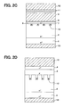
- FIG. 3A A simulated electric potential distribution in a cross section of an SiC semiconductor device including the P type deep layers 10 is illustrated in FIG. 3A .
- FIG. 3B A simulated electric potential distribution in a cross section of an SiC semiconductor device without the P type deep layers 10 is illustrated in FIG. 3B .
- Each of the cross sections is taken along a line corresponding to line IIA-IIA in FIG. 1 .
- a voltage at the P type base region 3 and front surfaces of the P type deep layers 10 is set to be 0 V. Equipotential lines are illustrated at 10 V intervals.
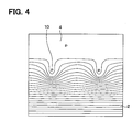
- FIG. 4 a simulated electric potential distribution in another cross section of the SiC semiconductor device including the P type deep layers 10 is illustrated in FIG. 4 .
- the cross section is taken along a line corresponding to line IID-IID in FIG. 1 .
- intervals between the equipotential lines are narrow in the gate oxide layer 8, especially at the bottom portion of the trench 6 as illustrated in FIG. 3B .
- the electric field in the gate oxide layer 8 is about 4.9 mV/cm.
- the equipotential lines are pressed down by the P type deep layers 10 as illustrated in FIG. 4 .
- the electric field in the gate oxide layer 8 is about 2.0 mV/cm as described above.
- the electric field is reduced to less than half of the electric filed in the SiC semiconductor device without the P type deep layers 10.
- the electric field concentration in the gate oxide layer 8 can be reduced by providing the P type deep layers 10.
- the N+ type substrate 1 made of SiC is prepared,
- the concentration of the N type impurity in the N+ type substrate 1 is about 1.0x10 19 cm -3 , for example.
- the thickness of the N+ type substrate 1 is about 300 ⁇ m, for example.
- the drain electrode 13 is formed on the rear surface of the N+ type substrate 1, the drain electrode 13 is formed.
- the N-type drift layer 2 is epitaxially formed.
- the concentration of the N type impurity in the N- type drift layer 2 is between about 3.0x10 15 cm -3 and about 7.0x10 15 cm -3 , for example.
- the thickness of the N- type drift layer 2 is about 15 ⁇ m.
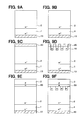
- a mask 20 is formed on the front surface of the N- type drift layer 2.
- the mask 20 is made of low temperature oxide (LTO), for example.
- LTO low temperature oxide
- opening portions are provided in the mask 20 by a photolithography process.
- the opening portions are provided at regions where the P type deep layers 10 will be formed.
- the P type impurities are ion-implanted through the mask 20 and are activated. Thereby, the P type deep layers 10 are formed.
- the P type impurities are boron or aluminum, for example.
- the impurity concentration in the P type deep layers 10 is between about 1.0x10 17 cm -3 and about 1.0x10 19 cm -3 , for example.
- the thickness of the P type deep layers 10 is between about 0.6 ⁇ m and about 1.0 ⁇ m, for example.
- the width of the P type deep layers 10 is between about 0.6 ⁇ m and about 1.0 ⁇ m.
- the P type base region 3 is formed on the N- type drift layer 2.
- the impurity concentration in the P type base region 3 is between about 5.0x10 16 cm -3 and about 2.0x10 19 cm -3 , for example.
- the thickness of the P type base region 3 is about 2.0 ⁇ m, for example.
- a first mask (not shown), for example, made of LTO is formed. Then, an opening portion is provided in the first mask by a photolithography process. The opening portion is provided at a portion where the N+ type source region 4 will be formed. Then, the N type impurities are ion-implanted.
- the N type impurities include nitrogen, for example.
- a second mask for example, made of LTO is formed. An opening portion is provided in the second mask by a photolithography process. The opening portion is provided at a portion where the P+ type body layer 5 will be formed. Then, the P type impurities are ion-implanted.
- the P type impurities include nitrogen, for example.
- the implanted ions are activated. Thereby, the N+ type source region 4 and the P+ type body layer 5 are formed.
- the impurity concentration at the surface portion of the N+ type source region 4 is about 1.0x10 21 cm -3 and the thickness of the N+ type source region 4 is about 0.3 ⁇ m, for example.
- the impurity concentration at the surface portion of the P+ type body layer 5 is about 1.0x10 21 cm -3 and the thickness of the P type body layer 5 is about 0.3 ⁇ m, for example.
- the second mask is removed.
- an etching mask (not shown) is formed on the N+ type source region 4 and the P+ type body layer 5. An opening portion is provided in the etching mask so that a region where the trench 6 will be provided is open. Then, an anisotropic etching process is performed using the etching mask. After that, an isotropic etching process and/or a sacrificial oxidation are performed if needed. Thereby, the trench 6 is provided. Then, the etching mask is removed.
- the N type channel layer 7 is epitaxially formed on the whole area of the surface of the substrate.
- the concentration of the N type impurities in the N type channel layer 7 is about 1.0x10 16 cm -3 , for example. Due to a plane direction dependence of the epitaxial growth, the N type channel layer 7 at the bottom portion of the trench 6 becomes thicker than the N type channel layer 7 on the sidewall of the trench 6. Then, unnecessary portion of the N type channel layer 7, that is, portion of the N type channel layer 7 formed on the P type base region 3, the N+ type source region 4, and the P+ type body layer 5 are removed.
- the gate oxide layer 8 is formed by thermal oxidation in a wet atmosphere, for example.
- a polysilicon layer doped with the N type impurities is formed on the surface of the gate oxide layer 8, for example, at 600 degrees centigrade so as to have a thickness of about 440 nm. Then, an etch back process is performed so that the gate oxide layer 8 and the gate electrode 9 remain in the trench 6.
- a process after forming the gate oxide layer 8 and the gate electrode 9 are similar to a known process. Therefore, the process after forming the gate oxide layer 8 and the gate electrode 9 is not illustrated.
- the interlayer insulating layer 12 is formed and the contact holes extending to corresponding ones of the N+ type source region 4 and the P+ type body layer 5 are provided in a cross section of the interlayer insulating layer 12.
- the contact hole extending to the gate electrode 9 is provided in another cross section of the interlayer insulating layer 12.
- a layer of an electrode material is formed on the interlayer insulating layer 12 so as to fill the contact holes and is pattern-formed. Thereby, the source electrode 11 and the gate wiring are formed and the MOSFET illustrated in FIG. 1 is formed.
- the P type deep layers 10 are not formed by providing trenches and epitaxially forming P type layers so as to fill the trenches.
- a planarization process after forming the P type layers is not required.
- a crystal defect which can possibly generate due to the planarization process, can be prevented.
- the P type deep layers 10 are formed by the ion implantation from the surface of the N- type drift layer 2.
- the ion implantation may be performed from the surface of the P type base region 3.
- the ion implantation does not require a high energy compared with a case where the ion implantation is performed from the surface of the P type base region 3.
- a crystal defect which can possibly be generated due to an ion implantation with a high energy, can be prevented.
- a device property is affected by a variation in a distance between the trench 6 and the P type deep layers 10.
- a mask for providing the trench 6 and a mask for providing the P type deep layers 10 are required to be positioned with a high degree of accuracy.
- the masks can possibly be out of alignment.
- an effect of a misalignment of the masks on the device property cannot be completely prevented.
- the longitudinal direction of the trench 6 and the longitudinal direction of the P type deep layers 10 are approximately perpendicular to each other.
- the device property is not affected by the misalignment of the masks. Thereby, a variation in a production property can be reduced and a yield can be improved.
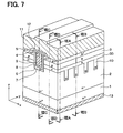
- an SiC semiconductor device will be described with reference to FIG. 7 to FIG. 8D .
- an N type current diffusion layer 30 is disposed between the N- type drift layer 2 and the P type base region 3 so as to be in contact with the N type channel layer 7.
- the N type current diffusion layer 30 includes, for example, phosphorous as N type impurities.
- a concentration of the N type impurities in the N type current diffusion layer 30 is set to be greater than the concentration of the N type impurity in the N- type drift layer 2.
- the concentration of the N type impurity in the N type current diffusion layer 30 may be greater than the concentration of the N type impurity in the N type channel layer 7.
- the impurity concentration in the N type current diffusion layer 30 is between about 2.0x10 15 cm -3 and about 1.0x10 17 cm -3 .
- the N type current diffusion layer 30 may have any thickness.
- the N type current diffusion layer 30 has a thickness of about 0.3 ⁇ m so that the trench 6 can penetrate through the N type current diffusion layer 30.
- the P type deep layers 10 are formed under the N type current diffusion layer 30.
- the N type current diffusion layer 30 separates the P type deep layers 10 and the P type base region 3.
- the P type deep layers 10 have a depth between about 0.6 ⁇ m and about 1.0 ⁇ m from a rear surface of the N type current diffusion layer 30.
- An impurity concentration, a width, and an interval of the P type deep layers 10 according to the present embodiment are similar to those of the P type deep layers 10 illustrated in FIG. 1 .
- the present MOSFET can be operated in a manner similar to the MOSFET illustrated in FIG. 1 .
- the present MOSFET When the present MOSFET is activated, electric current that flows in the N type channel layer 7 is extended in the N type current diffusion layer 30 in an approximately normal direction to the sidewall of the trench 6.
- the electric current disperses widely in the N- type drift layer 2.
- an on-resistance of the present MOSFET can be reduced compared with the MOSFET illustrated in FIG. 1 .
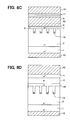
- FIG. 9A to FIG. 10F An exemplary method of manufacturing the MOSFET illustrated in FIG. 7 will be described with reference to FIG. 9A to FIG. 10F .
- the drain electrode 13 is formed on the rear surface of the N+ type substrate 1
- the N- type drift layer 2 is formed on the front surface of the N+ type substrate 1
- the P type deep layers 10 are formed in the N- type drift layer 2 in a manner similar to the process illustrated in FIG. 5A to FIG. 5D .
- FIG. 9E and FIG. 9F the N type current diffusion layer 30 is epitaxially formed on the front surface of the N- type drift layer 2 and the front surfaces of the P type deep layers 10.
- the P type base region 3 is epitaxially formed on the front surface of the N type current diffusion layer 30.
- the N+ type source region 4, the P+ type body layer 5, the trench 6, the N type channel layer 7, the gate oxide layer 8, and the gate electrode 9 are formed in a manner similar to the process illustrated FIG. 6A to FIG. 6F .
- the interlayer insulating layer 12, the contact holes, the source electrode 11, and the gate wiring are formed. Thereby, the MOSFET illustrated in FIG. 7 is formed.
- the N type current diffusion layer 30 is disposed between the N- type drift layer 2 and the P type base region 3 so as to be in contact with the N type channel layer 7.
- the P type deep layers 10 extend from the front surface of the N type current diffusion layer 30.
- the P type deep layers 10 penetrate through the N type current diffusion layer 30 and are contact with the P type base region 3.
- the P type deep layers 10 have a depth between about 0.6 ⁇ m and about 1.0 ⁇ m from the front surface of the N type current diffusion layer 30.
- An impurity concentration, a width, and an interval of the P type deep layers 10 according to the present embodiment are similar to those of the P type deep layers 10 illustrated in FIG. 1 .
- the MOSFET according to the present embodiment can be operated in a manner similar to the MOSFET illustrated in FIG. 1 .
- the MOSFET When the MOSFET is activated, electric current that flows in the N type channel layer 7 is extended in the N type current diffusion layer 30 in an approximately normal direction to the sidewall of the trench 6.
- the electric current disperse widely in the N- type drift layer 2 and the on-resistance can be reduced in a manner similar to the MOSFET illustrated in FIG. 7 .
- an electric potential of the P type deep layers 10 can be fixed to a source potential.
- an electric field relaxing effect of the MOSFET according to the present embodiment is greater than an electric field relaxing effect of the MOSFET illustrated in FIG. 7 , in which the P type deep layers 10 are separated from the P type base region 3 by the N type current diffusion layer 30 and the P type deep layers 10 are in a floating state.
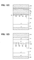
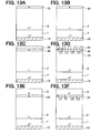
- FIG. 11 An exemplary manufacturing method of the MOSFET illustrated in FIG. 11 will be described with reference to FIG. 13A to FIG. 14F .
- the drain electrode 13 is formed on the rear surface of the N+ type substrate 1 and the N- type drift layer 2 is formed on the front surface of the N+ type substrate 1.
- the N type current diffusion layer 30 is epitaxially formed on the front surface of the N- type drift layer 2.
- the impurity concentration of the N type current diffusion layer 30 is greater than the impurity concentration of the N- type drift layer 2.
- the mask 20 is formed on the front surface of the N type current diffusion layer 30 and the P type deep layers 10 are formed in a manner similar to the process illustrated in FIG. 5C and FIG. 5D .
- a MOSFET included in the SiC semiconductor device according to the present embodiment may be an inversion type of the MOSFETs illustrated in FIG. 1 , FIG. 7 , or FIG. 11 .
- a MOSFET illustrated in FIG. 15 is an inversion type of the MOSFET illustrated in FIG. 1 .
- the N type channel layer 7 illustrated in FIG. 1 is not provided and the gate oxide layer 8 is formed on the surface of the trench 6.
- the gate oxide layer 8 is in contact with the P type base region 3 and the N+ type source region 4 at the sidewall of the trench 6.
- the MOSFET according to the present embodiment includes the P type deep layers 10.
- a drain voltage having a high voltage is applied to the present MOSFET, depletion layers at PN junctions between the P type deep layers 10 and the N- type drift layer 2 expand toward the N- type drift layer 2.
- a high voltage due to the drain voltage is restricted from entering the gate oxide layer 8.
- an electric field concentration in the gate oxide layer 8 especially, the electric field concentration in the gate oxide layer 8 at the bottom portion of the trench 6 can be reduced.
- the gate oxide layer 8 is restricted from being damaged.
- the MOSFET according to the present embodiment can be manufactured in a manner similar to the above-described manufacturing process. However, in the present embodiment, the N type channel layer 7 is not provided and the gate oxide layer 8 is formed directly on the surface of the trench 6.
- Each of the SiC semiconductor devices according to the first to fourth embodiments includes the N channel MOSFETs in which a first conductivity type is an N type and a second conductivity type is a P type.
- each of the SiC semiconductor devices may include P channel MOSFETs in which the conductivity types are reversed.
- each of the SiC semiconductor devices may include insulated gate bipolar transistors (IGBTs) each having a trench gate structure.
- IGBTs insulated gate bipolar transistors
- the conductivity type of the N+ type substrate 1 is changed from the N conductivity type to the P conductivity type.
- Other structure and a manufacturing method are similar to the above-described embodiments.
- the P type base region 3 and the N+ type source region 4 are formed before providing the trench 6.
- the P type base region 3 and the N+ type source region 4 may be formed by an ion implantation after forming the trench 6.
- the N+ type source region 4 in the first to third embodiments is formed by the ion implantation
- the N+ type source region 4 may be in contact with the gate oxide layer 8.
- the P type base region 3 is formed by the ion implantation
- the P type base region 3 can be separated from the sidewall of the trench 6.
- the N- type drift layer 2 that remains between the sidewall of the trench 6 and the P type base region 3 can be used as the N type channel layer 7.
- the P type base region 3 and the N+ type source region 4 may be formed by an ion implantation after forming the trench 6.
- the N+ type source region 4 and the P+ type body layer 5 may be epitaxially formed.
- the P type base region 3 is electrically coupled with the source electrode 11 through the P+ type body layer 5.
- the P+ type body layer 5 may be a contact part and the P type base region 3 may be electrically coupled with the source electrode 11 through the contact part.
- the gate oxide layer 8 formed by the thermal oxidation is provided as an example of a gate insulating layer.
- the gate insulating layer may be an oxide layer formed by another method or a nitride layer, for example.
- the drain electrode 13 may be formed after forming the source electrode 11.
- the impurity concentration of the N type current diffusion layer 30 may be equal to the impurity concentration of the N- type drift layer 2.
- the trench 6 is formed after forming the N type current diffusion layer 30 and a position of the bottom portion of the trench 6 is higher than a case where the N type current diffusion layer 30 is not provided.
- the position of the P type deep layers 10 is set be deeper than the bottom portion of the trench 6 more effectively, the electric field relaxing effect at the bottom portion of the trench 6 can be improved compared with the first embodiment.
- Each of the accumulation type MOSFETs according to the first to third embodiments includes the N type channel layer 7 around the trench gate.
- the N type channel layer 7 is epitaxially formed on the surface of the trench 6.
- the on-resistance of the accumulation type MOSFET may vary in the plane.
- the inversion type MOSFET according to the fourth embodiment does not include the N type channel layer 7.
- the on-resistance of the inversion type MOSFET does not vary in a plane.
- the breakdown voltage is basically determined by a depletion layer expanding along the trench 6 toward the N- type drift layer 2 and a depletion layer expanding from the P type deep layers 10 toward the N- type drift layer 2. However, at a portion away from the trench gate structure, the expanding amount of the depletion layer from the P type deep layers 10 toward the N- type drift layer 2 is reduced. Thus, the breakdown voltage at the portion away from the trench gate structure is determined by the depletion layer expanding from the P type base region 3 to the N- type drift layer 2.
- the expanding amount of the depletion layer expanding from the P type base region 3 toward the N- type drift layer 2 increases with the impurity concentration of the P type base region 3.
- the impurity concentration of the P type base region 3 is high, for example, when the impurity concentration of the P type base region 3 is about 1x10 17 cm -3 , a punching through at a reverse bias can be prevented and the breakdown voltage can be improved.
- an inversion channel is formed at the portion of the P type base region at a time when the channel region is provided.
- the impurity concentration of the P type base region 3 is high, a channel mobility may be reduced and the on-resistance may increase.
- the channel mobility can increase and the on-resistance can be reduced.
- the expanding amount of the depletion layer expanding from the P type base region 3 toward the N- type drift layer 2 may be reduced, and thereby a punching through may occur at the reverse bias.
- the breakdown voltage may be reduced when the impurity concentration of the P type base region 3 is low.
- the SiC semiconductor device according to the present embodiment includes a plurality of inversion type MOSFETs.
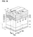
- One of the MOSFETs is illustrated in FIG. 16 .
- the MOSFETs are arranged in a plurality of rows so as to be adjacent to each other.
- the MOSFET includes an N+ type substrate 101 made of SiC.
- the N+ type substrate 1 includes, for example, phosphorus as N type impurities.
- An impurity concentration of the N+ type substrate 101 is, for example, about 1.0x10 19 cm -3 .
- the N+ type substrate 101 has a thickness of, for example, about 300 ⁇ m.
- an N- type drift layer 102 made of SiC is located on a front surface of the N+ type substrate 1.
- the N- type drift layer 2 includes, for example, phosphorus as N type impurities.
- An impurity concentration of the N- type drift layer 2 is, for example, between about 3.0x10 15 cm -3 and about 7.0x10 15 cm -3 .
- the N- type drift layer 102 has a thickness, for example, between about 10 ⁇ m and about 15 ⁇ m.
- the impurity concentration of the N- type drift layer 102 may be substantially constant in a thickness direction of the N- type drift layer 102.
- the impurity concentration of the N- type drift layer 102 may be varied in the thickness direction of the N- type drift layer 102.
- the impurity concentration of the N- type drift layer 102 may decrease toward a side away from the front surface of the N+ type substrate 101.
- the impurity concentration of a portion of the N-type drift layer 102 at a distance between about 3 ⁇ m and about 5 ⁇ m from the front surface of the N+ type substrate 101 may be greater than the impurity concentration of the other portion of the N- type drift layer 102 by about 2.0x10 15 cm -3 .
- an internal resistance of the N- type drift layer 102 can be reduced.
- an on-resistance of the MOSFET can be reduced.
- a P type base region 103 is located.
- an N+ type source region 104 and a P+ type contact layer 105 are located.
- a P+ type body layer 106 is located in the P type base region 103. The P+ type body layer 106 is located at a portion deeper than the N+ type source region 104 and the P+ type contact layer 105.
- the P type base region 103 includes, for example, boron or aluminum as P type impurities.
- the impurity concentration of the P type base region 103 is, for example, between about 5.0x10 15 cm -3 and about 5.0x10 16 cm -3 .
- the P type base region 103 has a thickness of, for example, 2.0 ⁇ m.
- the N+ type source region 104 includes, for example, phosphorous, as N type impurities.
- An impurity concentration of a surface portion of the N+ type source region 104 is, for example, about 1.0x10 21 cm -3 , for example.
- the N+ type source region 104 has a thickness of, for example, about 0.3 ⁇ m.
- the P+ type contact layer 105 includes, for example, boron or aluminum as P type impurities.
- An impurity concentration of a surface portion of the P+ type contact layer 105 is, for example, about 1.0x10 21 cm -3 .
- the P+ type contact layer 105 has a thickness of, for example, about 0.3 ⁇ m.
- the P+ type body layer 106 includes, for example, boron or aluminum as P type impurities.
- An impurity concentration of the P+ type body layer 106 is, for example, between about 1.0x10 18 cm -3 and about 1.0x10 20 cm -3 .
- the P+ type body layer 106 has a thickness, for example, between about 0.7 ⁇ m and about 1.1 ⁇ m.
- the N+ type source region 104 sandwiches a trench 107.
- the P+ type contact layer 105 sandwiches the N+ type source region 104 and the trench 107.
- the P+ type body layer 106 sandwiches the trench 107.
- the P+ type body layer 106 is away from a sidewall of the trench 107. A distance from the sidewall of the trench 107 to the P+ type body layer 106 is between about 0.4 ⁇ m and about 0.9 ⁇ m.
- the trench 107 penetrates the P type base region 103 and the N+ type source region 104 and reaches the N- type drift layer 102.
- the trench 107 has a width, for example, between about 1.4 ⁇ m and about 2.0 ⁇ m.
- the trench 107 has a depth greater than or equal to about 2.0 ⁇ m.
- the trench 107 has a depth about 2.4 ⁇ m.
- the P type base region 103 and the N+ type source region 104 are in contact with the sidewall of the trench 107.
- a surface of the trench 107 is covered with a gate oxide layer 108.
- a gate electrode 109 is formed so as to fill the trench 107.
- the gate electrode 109 is made of doped polysilicon.
- the gate oxide layer 108 is formed, for example, by thermally oxidizing an inner wall of the trench 107.
- the gate oxide layer 108 has a thickness of about 100 nm at the sidewall of the trench 107 and at a bottom portion of the trench 107.
- the trench gate structure is formed along a y-direction illustrated in FIG. 16 . That is, a longitudinal direction of the trench gate structure is the y-direction. A plurality of the trench gate structures is arranged in an x-direction that is approximately perpendicular to the longitudinal direction of the trench gate structure.
- the N+ type source region 104, the P+ type contact layer 105, and the P+ type body layer 106 are also formed along the longitudinal direction of the trench gate structure.
- a plurality of P type deep layers 110 is formed under the P type base region 103.
- the P type deep layers 110 are formed along an approximately normal direction to the sidewall of the trench 107 where the channel region is provided. That is, the P type deep layers 110 are formed along the x-direction approximately perpendicular to the longitudinal direction of the trench 107.
- the P type deep layers 110 extend to a depth deeper than the bottom portion the trench 107.
- the P type deep layers 10 extend to a depth between about 2.6 ⁇ m and about 3.0 ⁇ m from the front surface of the N-type drift layer 102, that is, between about 0.6 ⁇ m and about 1.0 ⁇ m from a bottom portion of the P type base region 103.
- a width of each of the P type deep layers 110 in the y-direction is, for example, between about 0.6 ⁇ m and about 1.0 ⁇ m.
- the P type deep layers 110 include, for example, boron or aluminum as P type impurities.
- An impurity concentration of the P type deep layers 110 is, for example, between about 1.0x10 17 cm -3 and about 1.0x10 19 cm -3 .
- the P type deep layers 110 are arranged in the longitudinal direction of the trench 107 so as to be parallel to each other.
- An interval of the P type deep layers 110 is, for example, between about 1.5 ⁇ m and about 3.0 ⁇ m. In the MOSFET according to the present embodiment, the interval of the P type deep layers 110 is about 2.0 ⁇ m.
- a source electrode 111 and a gate wiring are formed on surfaces of the N+ type source region 104, the P+ type contact layer 105, and the gate electrode 109.
- the source electrode 111 and the gate wiring are made of a plurality of metals, for example, an alloy of nickel and aluminum. At least portions of the source electrode 111 and the gate wiring being in contact with an N type SiC are made of a metal that can provide an ohmic connection between each of the source electrode 111 and the gate wiring and the N type SiC.
- the N type SiC includes the N+ type source region 104 and the gate electrode 109 if the gate electrode 109 includes N type impurities.
- At least portions of the source electrode 111 and the gate wiring being in contact with a P type SiC are made of a metal that can provide an ohmic connection between each of the source electrode 111 and the gate wiring and the P type SiC.
- the P type SiC includes the P+ type contact layer 105 and the gate electrode 109 if the gate electrode 109 includes P type impurities.
- the source electrode 111 and the gate wiring are formed on an interlayer insulating layer 112. Thus, the source electrode 111 and the gate wiring are electrically insulated.
- the source electrode 111 is electrically coupled with the N+ type source region 104 and the P+ type contact layer 105 through contact holes provided in the interlayer insulating layer 112.
- the gate wiring is electrically coupled with the gate electrode 109 though a contact hole provided in the interlayer insulating layer 112.
- a drain electrode 113 is formed on a rear surface of the N+ type substrate 101.
- the drain electrode 113 is electrically coupled with the N+ type substrate 101.
- an N-channel inversion type MOSFET having a trench gate structure is formed.
- the present inversion type MOSFET may be operated, for example, as described below.
- the channel region is not provided at a portion of the P type base region 103 located on the sidewall of the trench 107.
- the drain electrode 113 Even if a positive voltage is applied to the drain electrode 113, electrons are prevented from moving due to the PNP junction structure configured by the N- type drift layer 102, the P type base region 103, and the N+ type source region 104. Therefore, electric current does not flow between the source electrode 111 and the drain electrode 113.
- a depletion layer expands from a region between each of the P type base region 103 and the P type deep layers 110 and the N- type drift layer 102.
- a depletion layer also expands from a region between the trench gate structure and the N- type drift layer 102.
- the impurity concentration of the P type base region 103 is low, the expanding amount of the depletion layer that expands toward the N- type drift layer 102 may be reduced.
- the P+ type body layer 106 is provided in addition to the P type base region 103.
- the impurity concentration of the P+ type body layer 106 is greater than the impurity concentration of the P type base region 103.
- the punching through can be prevented by the depletion layer expanding from a region between the P type base region 103 including the P+ type body layer 106 and the N- type drift layer 102 in addition to the depletion layer expanding from the region between the P type deep layers 110 and the N- type drift layer 102 and the depletion layer expanding from the region between the trench gate structure and the N- type drift layer 102.
- the breakdown voltage of the MOSFET can be increased by providing the P+ type body layer 106 having the impurity concentration greater than the P type base region 103.
- the MOSFET includes the P type deep layers 110 extending to the depth deeper than the trench 107.
- the depletion layer expands toward the N- type drift layer 102 at the PN junction between the P type deep layers 110 and the N- type drift layer 102.
- a high voltage due to the drain voltage is restricted from being applied to the gate oxide layer 108.
- the gate electrode 109 When the MOSFET is activated, for example, when the gate voltage is about 20 V, the drain voltage is about 1 V, and the source voltage is about 0V, the gate electrode 109 is applied with the gate voltage of about 20 V. Thus, an inversion channel is formed at a portion of the P type base region 103 adjacent to the sidewall of the trench 107, and thereby the channel region is provided. Electrons induced from the source electrode 111 flows to the N- type drift layer 102 through the N+ type source region 4 and the channel region in the P type base region 103. Thereby, electric current flows between the source electrode 111 and the drain electrode 113.
- the MOSFET according to the present embodiment includes the P+ type body layer 106.
- the impurity concentration of the P type base region 103 can be reduced.
- the inversion channel can be easily formed at the portion of the P type base region 103, and an area of the channel region can be increased.
- the channel mobility can be increased.
- the P+ type body layer 106 is formed at the portion of the P type base region 103 away from the trench 107.
- the inversion channel can be formed at the portion of the P type base region 103 adjacent to the sidewall of the trench 107 without being affected by the P+ type body layer 106.
- the on-resistance of the MOSFET can be reduced compared with a case where the P+ type body layer 106 is not provided.
- the impurity concentration of the P type base region 103 is required to be about 1.0x10 17 cm -3 .
- the channel mobility is about 120 cm 2 /V ⁇ s and the on-resistance is 5.1 m ⁇ cm 2 .
- the MOSFET including the P+ type body layer 106 can have the predetermined breakdown voltage when the impurity concentration of the P type base region 103 is about 1.0x10 16 cm -3 .
- the channel mobility is about 210 cm 2 /V ⁇ s and the on-resistance can be reduced to about 3.5 m ⁇ cm 2 .
- FIG. 18B and FIG. 19 A behavior of the MOSFET when the MOSFET is deactivated can be simulated as was demonstrated by the inventors.
- the simulated results are illustrated in FIG. 18B and FIG. 19 .
- FIG. 19 the simulated result in a case where the MOSFET includes the P type deep layers 110 and the P+ type body layer 106 is not provided and a case where the MOSFET includes both of the P type deep layers 110 and the P+ type body layer 106 are illustrated.
- the equipotential lines are illustrated at 10 V intervals.
- the impurity concentration of the P type base region 103 is about two times greater than the impurity concentration of the N- type drift layer 102 and the P+ type body layer 106 and the P type deep layers 110 are not provided, when a depletion layer expands toward the N- type drift layer 102 by about 4 ⁇ m, the depletion layer expands toward the P type base region 103 by about 2 ⁇ m. In this case, a punching through may easily occur.
- a depletion layer also expands from the P type deep layers 110.
- the impurity concentration of the P type deep layers 110 is about 100 times greater than the impurity concentration of the N- type drift layer 102
- the depletion layer expands mostly toward the N- type drift layer 102.
- a high breakdown voltage can be provided as seen from a distribution of the equipotential lines at a bottom portion of the P type deep layers illustrated in FIG. 18B .
- the expanding amount of the depletion layer expanding toward the N- type drift layer 102 may be reduced at portions where the P type deep layers 110 are not formed, that is, at portions between the P type deep layers 110.
- a high breakdown voltage may not be provided at the portions between the P type deep layers 110.
- the depletion layer also expands from the trench 107 due to a difference in a work function of the gate oxide layer 108 and SiC. Thus, a high breakdown voltage can be provided at portion adjacent to the trench gate structure.
- a high breakdown voltage may not be provided at another portion away from the trench gate structure. That is, the punching though may not be prevented only by the depletion layer expanding from the P type deep layers 110 and the trench gate structure toward the N- type drift layer 2.
- a punching through current may flow as illustrated in a current density distribution in FIG. 19 .
- the MOSFET according to the present embodiment includes the P+ type body layer 106 in addition to the P type deep layers 110.
- the impurity concentration of the P+ type body layer 106 can be about 1000 times greater than the impurity concentration of the N- type drift layer 102.
- the depletion layer expands mostly toward the N- type drift layer 102. Therefore, as seen from the equipotential line distribution in FIG. 19 , a high breakdown voltage can be provided at portions where the P type deep layers 10 are not formed.
- the MOSFET according to the present embodiment can have a high breakdown voltage greater than or equal to about 1200 V.
- the depletion layer expands from the P+ type body layer 106 and the P type base region 103 toward the N- type drift layer 102 in addition to the depletion layer expanding from the P type deep layers 110 and the trench gate structure toward the N- type drift layer 102.
- the high breakdown voltage can be provided at the portion away from trench gate structure in addition to the portion adjacent to the trench gate structure and the portions where the P type deep layers 110 are formed. Thereby, a flow of a punching through current can be prevented as seen from the current density distribution illustrated in FIG. 19 .
- the on-resistance may increase.
- the increase of the on-resistance is not so large and can be controlled by changing the width of the P type deep layers 110 and the interval of the P type deep layers 110.
- the increase of the on-resistance does not become an issue.
- the interval of the P type deep layers 110 can be increased due to the P+ type body layer 106.
- the on-resistance can be effectively reduced.
- FIG. 16 An exemplary method of manufacturing the MOSFET illustrated in FIG. 16 will be described with reference to FIG. 20A to FIG. 21F .
- the N+ type substrate 101 is prepared.
- the impurity concentration of N+ type substrate 101 is, for example, about 1.0x10 19 cm -3 .
- the N+ type substrate 101 has a thickness of, for example, about 300 ⁇ m.
- the drain electrode 113 is formed on the rear surface of the N+ type substrate 101.
- the N- type drift layer 102 is epitaxially formed.
- the impurity concentration of the N- type drift layer 102 is, for example, between about 3.0x10 15 cm -3 and about 7.0x10 15 cm -3 .
- the N- type drift layer 2 has a thickness of, for example, about 15 ⁇ m.
- a mask 120 is formed on the front surface of the N- type drift layer 102.
- the mask 120 is made of LTO, for example.
- opening portions are provided in the mask 120 by a photolithography process.
- the opening portions are provided at regions where the P deep layers 110 will be formed.
- the P type impurities are ion-implanted through the mask 120 and are activated. Thereby, the P type deep layers 110 are formed.
- the P type impurities are, for example, boron or aluminum.
- the impurity concentration of the P type deep layers 110 is, for example, between about 1.0x10 17 cm -3 and about 1.0x10 19 cm -3 .
- the thickness of the P deep layers 110 is, for example, between about 0.6 ⁇ m and about 1.0 ⁇ m.
- the width of the P type deep layers 110 is, for example, between about 0.6 ⁇ m and about 1.0 ⁇ m.
- the interval of the P type deep layer 110 is between about 2.0 ⁇ m and about 3.0 ⁇ m, for example, about 2.0 ⁇ m.
- the P type base region 103 is epitaxially formed on the N- type drift layer 102.
- the impurity concentration of P type base region 103 is, for example, between about 5.0x10 15 cm -3 and about 5.0x10 16 cm -3 .
- the thickness of the P type base region 103 is, for example, about 2.0 ⁇ m.
- a first mask for example, made of LTO is formed on the P type base region 103.
- An opening portion is provided in the first mask by a photolithography process. The opening portion is provided at a portion where the P+ type body layer 106 will be formed so that the P+ type body layer 106 will be away from the sidewall of the trench 107. Then, the P type impurities such as boron or aluminum are ion-implanted.
- a second mask for example, made of LTO is formed on the P type base region 103.
- An opening portion is provided in the second mask by a photolithography process. The opening portion is provided at a portion where the N+ type source region 104 will be formed. Then, the N type impurities such as phosphorous are ion-implanted.
- a third mask is formed and an opening portion is provided in the third mask by a photolithography process.
- the opening portion is provided at a portion where the P+ type contact layer 105 will be formed.
- the P type impurities such as boron or aluminum are ion-implanted.
- the implanted ions are activated. Thereby, the N+ type source region 104, the P+ type contact layer 105, and the P+ type body layer 106 are formed.
- the impurity concentration at the surface portion of the N+ type source region 104 is about 1.0x10 21 cm -3 and the thickness of the N+ type source region104 is about 0.3 ⁇ m, for example.
- the impurity concentration at the surface portion of the P+ type contact layer 105 is about 1.0x10 21 cm -3 and the thickness of the source region is about 0.3 ⁇ m, for example.
- the impurity concentration of the P+ type body layer 106 is between about 1.0x10 18 cm -3 and about 1.0x10 20 cm -3 , and the thickness of the P+ type body layer 106 is between about 0.7 ⁇ m and about 1.1 ⁇ m, for example. After that, the third mask is removed.
- an etching mask is formed on the N+ type source region 104 and the P+ type contact layer 105.
- An opening portion is provided in the etching mask.
- the opening portion is provided at a portion where the trench 107 will be formed so that the trench 107 will be away from the P+ type body layer 106.
- an anisotropic etching process is performed using the etching mask.
- an isotropic etching process and/or a sacrificial oxidation are performed if needed.
- the distance between the sidewall of the trench 107 and the P+ type body layer 106 is, for example, between about 0.4 ⁇ m and between about 0.9 ⁇ m.
- the etching mask is removed.
- the masks can possibly be out of alignment. Thereby, a positional relationship between the P+ type body layer 106 and the trench 107 may vary and the distance between the sidewall of the trench 107 and the P+ type body layer 106 may vary about 0.2 ⁇ m at the maximum.
- the distance between the sidewall of the trench 107 and the P+ type body layer 106 is required to be greater than or equal to about 0.1 ⁇ m so that the inversion channel can be formed at the portion of the P type base region 103 without being affected by the impurity concentration of the P+ type body layer 106 and the channel mobility is not reduced.
- the distance between the sidewall of the trench 107 and the P+ type body layer 106 is greater than or equal to 0.4 ⁇ m.
- the distance will not be less than 0.2 ⁇ m. Therefore, the inversion channel can be formed at the portion of the P type base region 103 without being affected by the impurity concentration of the P+ type body layer 106 and the channel mobility does not reduced.
- the breakdown voltage is provided only by the depletion layer expanding from the trench gate structure and the P+ type body layer 106.
- the depletion layer expanding from the trench gate structure and the P+ type body layer 106 is difficult to provide a high breakdown voltage between the trench gate structure and the P+ type body layer 106.
- the depletion layer expanding from the trench gate structure and the P+ type body layer 106 can provide a high breakdown voltage.
- the distance between the sidewall of the trench 107 and the P+ type body layer 106 is set to be about 0.3 ⁇ m, the distance may vary between about 0.1 ⁇ m and about 0.5 ⁇ m when the masks are out of alignment.
- the inversion channel may not be formed at the P type base region 103 due to the impurity concentration of the P type body layer 106.
- the depletion layer expanding from the trench gate structure and the P+ type body layer 106 may not provide the high breakdown voltage between the trench gate structure and the P+ type body layer 106.
- the MOSFET according to the present embodiment includes both the P+ type body layer 106 and the P type deep layers 110.
- the gate oxide layer 108 is formed on the whole surface of the substrate including an inside of the trench 107.
- the gate oxide layer 108 is formed by thermal oxidation in a wet atmosphere.
- a polysilicon layer doped with the N type impurities is formed on the surface of the gate oxide layer 108, for example, at 600 degrees centigrade so as to have a thickness of about 440 nm. Then, an etch back process is performed so that the gate oxide layer 108 and the gate electrode 109 remain in the trench 107.
- a process after forming the gate oxide layer 108 and the gate electrode 109 are similar to a known process. Therefore, the process after forming the gate oxide layer 108 and the gate electrode 109 is not illustrated.
- the interlayer insulating layer 112 is formed and the contact holes extending to corresponding ones of the N+ type source region 104 and the P+ type contact layer 105 are provided in a cross section of the interlayer insulating layer 112.
- the contact hole extending to the gate electrode 109 is provided in another cross section of the interlayer insulating layer 112.
- a layer of an electrode material is formed on the interlayer insulating layer 112 so as to fill the contact holes.
- the layer of the electrode material is pattern-formed so that the source electrode 111 and a gate wiring are formed. Thereby, the MOSFET illustrated in FIG. 16 is formed.
- the P type deep layers 110 are not formed by providing trenches and epitaxially forming P type layers so as to fill the trenches.
- a planarization process after forming the P type layers is not required.
- a crystal defects which can possibly generate due to the planarization process, can be prevented.
- the P type deep layers 110 are formed by the ion implantation from the surface of the N- type drift layer 102.
- the ion implantation may be performed from the surface of the P type base region 103.
- the ion implantation does not require a high energy compared with a case where the ion implantation is performed from the surface of the P type base region 103.
- crystal defects which can possibly generate due to an ion implantation with a high energy, can be prevented.
- a device property is affected by a variation in a distance between the trench 107 and the P type deep layers 110.
- a mask for providing the trench 107 and a mask for providing the P type deep layers 110 are required to be positioned with a high degree of accuracy.
- the masks can possibly be out of alignment.
- an effect of a misalignment of the masks on the device property cannot be completely prevented.
- the longitudinal direction of the trench 107 and the longitudinal direction of the deep layers 110 are approximately perpendicular to each other.
- the device property is not affected by the misalignment of the masks. Thereby, a variation in the device property can be restricted and a yield can be improved.
- the distance between the sidewall of the trench 107 and the P+ type body layer 106 is set to be between about 0.4 ⁇ m and about 0.9 ⁇ m.
- the width of each of the P type deep layers 110 is about 1.5 ⁇ m
- the interval of the P type deep layers 110 is about 2.0 ⁇ m
- the distance between the sidewall of the trench 107 and the P+ type body layer 106 is between about 0.4 ⁇ m and about 0.9 ⁇ m
- the distance between the sidewall of the trench 107 and the P+ type body layer 106 can be set in accordance with the width and the interval of the P type deep layers 110.
- the width of the P type deep layers 110 is about 1.5 ⁇ m and the interval of the P type deep layers 110 is about 2.0 ⁇ m
- a breakdown voltage is greater than or equal to about 1200 V, as illustrated in FIG. 22 .
- the on-resistance is about 4 m ⁇ cm 2 , as illustrated in FIG. 23 .
- the width of the P type deep layers 110 is about 1.5 ⁇ m and the interval of the P type deep layers 110 is about 3.0 ⁇ m
- a breakdown voltage is greater than or equal to about 1200 V, as illustrated in FIG. 22 .
- the on-resistance is about 4 m ⁇ cm 2 , as illustrated in FIG. 23 .
- the breakdown voltage can be improved and the on-resistance can be reduced by setting the distance between the trench 107 and the P+ type body layer 106 in accordance with the width and the intervals of the P type deep layers 110.
- the SiC semiconductor device includes the N-channel type MOSFET, as an example.
- the SiC semiconductor device may include a P-channel type MOSFET in which conductivity types of the components are reversed.
- the SiC semiconductor device may include IGBTs each having a trench gate structure. In a case where the SiC semiconductor device include the IGBTs, the conductivity type of the N+ type substrate 101 is changed from the N conductivity type to the P conductivity type.
- Other structure and a manufacturing method are similar to the above-described method.
- the P type base region 103, the N+ type source region 104, and the P+ type body layer 106 are formed before providing the trench 107.
- the P type base region 103, the N+ type source region 104, and the P+ type body layer 106 may be formed by ion implantation after providing the trench 107.
- the gate oxide layer 108 formed by the thermal oxidation is provided as an example of a gate insulating layer.
- the gate insulating layer may be an oxide layer formed by another method or a nitride layer, for example.
- the drain electrode 113 may be formed after forming the source electrode 111.
- the P type deep layers 110 are formed along the approximately normal direction of the sidewall of the trench 107, as an example.
- the P type deep layers 110 may also be formed along a direction inclined to the sidewall of the trench 107.
- a part of the P type deep layers 110 may be arranged in a direction inclined to one side from the normal direction of the sidewall of the trench 107 and the other part of the P type deep layers 110 may be arranged in a direction inclined to the opposite side of the one side from the normal direction.
- the part of the P type deep layers 110 cross the other part of the P type deep layers 110, and thereby the P type deep layers 110 are arranged in a lattice pattern.
- At least the longitudinal direction of the P type deep layers 110 is set so as to cross the longitudinal direction of the trench 107. That is, when the trench 107 is provided along a first direction, the P type deep layers 110 are formed along a second direction crossing the first direction.
- the P+ type body layer 106 is located at a portion deeper than the N+ type source region 104 and shallower than the P type base region 103, as an example.
- the P+ type body layer 106 may also be located at a portion deeper than the P type base region 103.
- the P+ type body layer 106 may also be separated from the P+ type contact layer 105.
- An SiC semiconductor device illustrated in FIG. 24 includes a plurality of trenches 201 arranged in a stripe pattern.
- the SiC semiconductor device further includes a plurality of P type deep layers 202.
- the P type deep layers 202 are arranged in a stripe pattern along an approximately normal direction to the longitudinal direction of the trenches 201 and are arranged in parallel with a planer direction of a substrate.
- the SiC semiconductor device includes a cell section Sa where the trenches 201 and the P type deep layers 202 are formed and a peripheral section Sb surrounding the cell section Sa.
- a mesa structure portion 206 is provided at the peripheral section Sb. As illustrated in FIG. 25A and FIG. 25B , the mesa structure portion 206 is recessed to a portion deeper than a P type base region 203 and a P+ type contact layer 204 and reaches an N- type drift layer 205.
- a P type RESURF (reduced surface field) layer 207 is located at a boundary portion between the cell section Sa and the peripheral section Sb.
- the P type RESURF layer 207 is formed from a sidewall of a stepped part of the mesa structure portion 206 and to a bottom surface of the stepped part.
- the P type RESURF layer 207 surrounds an outer edge portion og the cell section Sa.
- a plurality of P type guard ring layers 208 surround the P type RESURF layer 207.
- An N+ type layer 209 surrounds the P type RESURF layer 207 and the P type guard ring layers 208.
- a same potential ring electrode 210 is electrically coupled with the N+ type layer 209. Thereby, a peripheral high-voltage part is formed.
- a breakdown voltage of the semiconductor device illustrated in FIG. 25 can be simulated as was performed by the inventors.
- a breakdown occurs at a P type deep layer 202a located at the outer edge portion of the cell section Sa and an impact ionization-rate distribution increases at a portion adjacent to the P type deep layer 202a.
- a high breakdown voltage can be provided by depletion layers expanding from each of the adjacent P type deep layers 202 and a depletion layer expanding from the P type base region 203.
- equipotential lines are restricted from entering the P type base region 203.
- the P type deep layer 202a located at the outer edge portion of the cell section Sa is arranged on outside of the other P type deep layers 202.
- the equipotential lines may enter an upper portion of the P type base region 203.
- the outer edge portion of the cell section Sa is difficult to have a high breakdown voltage.
- a breakdown field strength of SiC depends on a plane direction.
- a vertical direction Da of the SiC substrate that is, a direction from a rear surface to a front surface of the SiC substrate is a direction of a (0001)-face.
- the SiC semiconductor device can have a high breakdown voltage when an electric field is applied to the SiC semiconductor device in a state where a direction of equipotential lines corresponds to the planer direction of the substrate.
- the equipotential lines incline with respect to the planer direction of the substrate.
- the electric field Db is applied to the P type deep layer 202a in a state that the electric field Db inclines from the vertical direction Da of the SiC substrate by about 30 degrees.
- the breakdown field strength may be reduced by about 20 percent compared with a case where the direction of the electric field corresponds to the direction of the (0001)-face.
- the portion adjacent to the P type deep layer 202a for example, a portion surrounded by the circle Rz may be damaged.
- the SiC semiconductor device includes a cell section Sa and a peripheral section Sb surrounding the cell section Sa.
- a cell section Sa a plurality of MOSFETs are formed.
- a peripheral high-voltage part is formed in the cell section Sa.
- the SiC semiconductor device includes an N+ type substrate 301 made of SiC.
- a main surface of the N+ type substrate 301 is a Si-face, that is, a vertical direction of the N+ type substrate 301 is a (0001)-face.
- the N+ type substrate 301 includes, for example, phosphorous as N type impurities.
- An impurity concentration of the N+ type substrate 301 is, for example, about 1.0x10 19 cm -3 .
- the N+ type substrate 301 has a thickness of, for example, about 300 ⁇ m.
- an N- type drift layer 302 made of SiC is located on a front surface of the N+ type substrate 301.
- the N- type drift layer 302 includes, for example, phosphorus as N type impurities.
- An impurity concentration of the N- type drift layer 302 is, for example, between about 3.0x10 15 cm -3 and about 7.0x10 15 cm -3 .
- the N- type drift layer 302 has a thickness, for example, between about 10 ⁇ m and about 15 ⁇ m.
- the impurity concentration of the N- type drift layer 302 may be substantially constant in a thickness direction of the N- type drift layer 302.
- the impurity concentration of the N- type drift layer 302 may be varied in the thickness direction of the N- type drift layer 302.
- the impurity concentration of the N-type drift layer 302 may decrease toward a side away from the front surface of the N+ type substrate 301.
- the impurity concentration of a portion of the N- type drift layer 302 at a distance between about 3 ⁇ m and about 5 ⁇ m from the front surface of the N+ type substrate 301 may be greater than the impurity concentration of the other portion of the N- type drift layer 302 by about 2.0x10 15 cm -3 .
- an internal resistance of the N- type drift layer 302 can be reduced.
- an on-resistance can be reduced.
- a P type base region 303 is located.
- an N+ type source region 304 and a P+ type contact layer 305 are located.
- the P type base region 303 includes, for example, boron or aluminum as P type impurities.
- the impurity concentration of the P type base region 303 is, for example, between about 5.0x10 15 cm -3 and about 5.0x10 16 cm -3 .
- the P type base region 103 has a thickness of, for example, about 2.0 ⁇ m.
- the N+ type source region 304 includes, for example, phosphorous as N type impurities.
- An impurity concentration of a surface portion of the N+ type source region 304 is, for example, about 1.0x10 21 cm -3 .
- the N+ type source region 304 has a thickness of, for example, about 0.3 ⁇ m.
- the P+ type contact layer 305 includes, for example, boron or aluminum as P type impurities.
- An impurity concentration of a surface portion of the P+ type contact layer 305 is, for example, about 1.0x10 21 cm -3 .
- the P+ type contact layer 305 has a thickness of, for example, about 0.3 ⁇ m.
- the N+ type source region 304 sandwiches a trench 306.
- the P+ type contact layer 305 sandwiches the N+ type source region 304 and the trench 306.
- the trench 306 penetrates the P type base region 303 and the N+ type source region 4 and reaches the N- type drift layer 302.
- the trench 306 has a width between about 1.4 ⁇ m and about 2.0 ⁇ m and has a depth greater than or equal to about 2.0 ⁇ m, for example, 2.4 ⁇ m.
- the P type base region 303 and the N+ type source region 304 are in contact with the sidewall of the trench 306.
- a surface of the trench 306 is covered with a gate oxide layer 308.
- a gate electrode 309 is formed so as to fill the trench 306.
- the gate electrode 309 is made of doped polysilicon.
- the gate oxide layer 308 is formed, for example, by thermally oxidizing an inner wall of the trench 306.
- the gate oxide layer 308 has a thickness about 100 nm at the sidewall of the trench 306 and at a bottom portion of the trench 306.
- the trench gate structure is formed along a y-direction illustrated in FIG. 29 . That is, a longitudinal direction of the trench gate structure is the y-direction. A plurality of the trench gate structures is arranged in an x-direction that is approximately perpendicular to the longitudinal direction of the trench gate structure.
- the N+ type source region 304, the P+ type contact layer 305 are also formed along the longitudinal direction of the trench gate structure.
- a P type deep layer 310 is located under the P type base region 303.
- the P type deep layer 310 has a plurality of stripe portions and an outer edge portion surrounding the stripe portion.
- the stripe portions of the P type deep layer 310 are formed along an approximately normal direction to the sidewall of the trench 306 where the channel region is provided. That is, the stripe portions of the P type deep layer 310 are formed in parallel with the planer direction of the N+ type substrate 301 along the x-direction approximately perpendicular to the longitudinal direction of the trench 306.
- the P type deep layer 310 extends to a depth deeper than the bottom portion the trench 306.
- the P type deep layer 310 extends to a portion between about 2.6 ⁇ m and about 3.0 ⁇ m from the front surface of the N- type drift layer 302, that is, between about 0.6 ⁇ m and about 1.0 ⁇ m from a bottom portion of the P type base region 303.
- a width of each of the stripe portions of the P type deep layer 310 in the y-direction is between about 0.6 ⁇ m and about 1.0 ⁇ m.
- the P type deep layer 310 includes, for example, boron or aluminum as P type impurities.
- An impurity concentration of the P type deep layer 310 is between about 1.0x10 17 cm -3 and about 1.0x10 19 cm -3 , for example, about 5.0x10 17 cm -3 .
- the stripe portions of the P type deep layer 310 are arranged in the longitudinal direction of the trench gate structure in a stripe pattern.
- the stripe portions of The P type deep layer 310 are parallel to each other and an interval of the stripe portions is, for example, between about 1.5 ⁇ m and about 3 ⁇ m.
- the outer edge portion of the P type deep layer 310 is formed at the whole area of the outer edge portion of the cell section Sa and reaches the peripheral section Sb.
- the P type base region 303 and the P+ type contact layer 305 are formed above the P type deep layer 310 to the portion that is not active, that is, the outer edge portion of the cell section Sa. Also at the portion that is not active, a source electrode 311 is electrically coupled with the P+ type contact layer 305.
- the source electrode 311 and a gate wiring are formed on surfaces of the N+ type source region 304, the P+ type contact layer 305, and the gate electrode 309.
- the source electrode 311 and the gate wiring are made of a plurality of metals, for example, an alloy of nickel and aluminum. At least portions of the source electrode 311 being in contact with an N type SiC are made of a metal that can provide an ohmic connection between each of the source electrode 311 and the N type SiC. At least portions of the source electrode 311 being in contact with a P type SiC are made of a metal that can provide an ohmic connection between each of the source electrode 311 and the P type SiC.
- the source electrode 311 and the gate wiring are formed on an interlayer insulating layer 312. Thus, the source electrode 311 and the gate wiring are electrically insulated.
- the source electrode 311 is electrically coupled with the N+ type source region 304 and the P+ type contact layer 305 through contact holes provided in the interlayer insulating layer 312.
- the gate wiring is electrically coupled with the gate electrode 309 though a contact hole provided in the interlayer insulating layer 312.
- a drain electrode 313 is formed on a rear surface of the N+ type substrate 301.
- the drain electrode 313 is electrically coupled with the N+ type substrate 301. In this way, an N-channel inversion type MOSFET having a trench gate structure is formed.
- a mesa structure portion 314 is provided.
- the mesa structure portion 314 is recessed to a portion deeper than the P type base region 303 and the P+ type contact layer 305 and reaches the N- type drift layer 302.
- the mesa structure portion 314 has a depth, for example, between about 2.1 ⁇ m and about 2.5 ⁇ m.
- a P type RESURF layer 315 is located at a boundary portion between the cell section Sa and the peripheral section Sb.
- the P type RESURF layer 315 is formed from a sidewall of a stepped part of the mesa structure portion 314 to a bottom surface of the stepped part.
- the P type RESURF layer 315 surrounds the outer edge portion of the cell section Sa.
- a plurality of P type guard ring layers 316 surround the P type RESURF layer 315.
- An N+ type layer 317 surrounds the P type RESURF layer 315 and the P type guard ring layers 316.
- a same potential ring electrode 318 is electrically coupled with the N+ type layer 317. Thereby, the peripheral high-voltage part is formed.
- the P type RESURF layer 315 is formed from the boundary portion between the cell section Sa and the peripheral section Sb toward an outside of the cell section Sb, for example, by about 20 ⁇ m.
- a part of the P type RESURF layer 315 formed on the sidewall of the stepped part of the mesa structure portion 314 has a thickness of about 0.7 ⁇ m in an approximately horizontal direction and includes P type impurities of about 1.0x10 17 cm -3 .
- a part of the P type RESURF layer 315 formed on the bottom surface of the recess part of the mesa structure portion 314 has a depth of about 0.7 um from the bottom surface and includes P type impurities of about 4.0x10 17 cm -3 .
- the depth of the P type deep layers 310 from the surface of the N- type drift layer 302 is, for example, between about 2.6 ⁇ m and about 3.0 ⁇ m.
- the depth of the P type deep layer 310 from the bottom surface of the recess part of the mesa structure portion 314 is similar to the depth of the P type RESURF layer 315 from the bottom surface of the recess part of the mesa structure portion 314.
- the outer edge portion of the P type deep layer 310 is formed toward the peripheral section Sb.
- the trench gate structures and the stripe portions of the P type deep payer 310 that are arranged in the stripe pattern are surrounded by the outer edge portion of the P type deep layer 310.
- the outer edge portion of the P type deep layer 310 is connected with the P type RESURF layer 315.
- the P type RESURF layer 315 is surrounded, for example, by six P type guard ring layers 316.
- the most inner layer is located, for example, at about 0.5 ⁇ m from the P type RESURF layer 315.
- a width of each of the P type guard ring layers 316 is, for example, about 2 ⁇ m.
- An interval of the P type guard ring layers 316 is, for example, about 1 ⁇ m.
- a depth of each of the P type guard ring layers 316 is, for example, about 0.7 ⁇ m.
- Each of the P type guard ring layers 316 includes P type impurities of 1.0x10 18 cm -3 , for example.
- the MOSFET according to the present embodiment may be operated, for example, as described below.
- the channel region is not provided at a portion of the P type base region 303 located on the sidewall of the trench 306.
- the drain electrode 313 electrons are prevented from moving due to the PNP junction structure configured by the N- type drift layer 302, the P type base region 303, and the N+ type source region 304. Therefore, electric current does not flow between the source electrode 311 and the drain electrode 313.
- the gate electrode 309 When the MOSFET is activated, for example, when the gate voltage is about 20 V, the drain voltage is about 1 V, and the source voltage is about 0 V, the gate electrode 309 is applied with the gate voltage of about 20 V. Thus, the inversion channel is formed at a portion of the P type base region 303 adjacent to the sidewall of the trench 306, and thereby the channel region is provided. Electrons induced from the source electrode 311 flows to the N- type drift layer 302 through the N+ type source region 304 and the channel region in the P type base region 303. Thereby, electric current flows between the source electrode 311 and the drain electrode 313.
- the impurity concentration of the P type deep layer 310 is, for example, about 5.0x10 17 cm -3 and the impurity concentration of the P type RESURF layer 315 is, for example, about 4.0x10 17 cm -3 .
- the impurity concentrations of the P type deep layer 310 and the P type RESURF layer 315 are about 100 times greater than the impurity concentration of the N- type drift layer 302. Therefore, the depletion layers expand mostly toward the N- type drift layer 302.
- the depth of the P type deep layer 310 is similar to the depth of the P type RESURF layer 315.
- the depletion layer expanding from the joint portion of the outer edge portion of the P type deep layer 310 and the N- type drift layer 302 is easily connected with the depletion layer expanding from the joint portion of the P type RESURF layer 315 and the N- type drift layer 302, and the depletion layer expands to the P type guard ring layers 316.
- Equipotential lines in the depletion layer are substantially horizontal at the joint portion of the outer edge portion of the P type deep layer 310 and the P type RESURF layer 315.
- an electric field concentration does not occur at the joint portion of the P type deep layer 310 and the P type RESURF layer 315 but at a portion in the vicinity of the P type guard ring layers 316.
- FIG. 32A a part in the vicinity of the joint portion of the P type deep layer 310 and the P type RESURF layer 315 is illustrated in FIG. 32A .
- the drain voltage Vd is about 200 V, about 400 V, and about 1200 V
- the electric potential distribution at the part in the vicinity of the joint portion of the P type deep layer 310 and the P type RESURF layer 315 become as illustrated in FIG. 32B, FIG. 32C , and FIG. 32D , respectively.
- equipotential lines are illustrated at 70 V intervals.
- the equipotential lines are substantially horizontal to a planer direction of the N+ type substrate 301 at the joint portion of the P type deep layer 310 and the P type RESURF layer 315.
- Electric field applies in a vertical direction of the equipotential lines.
- the electric filed applies in a direction approximately vertical to the planer direction of the N+ type substrate 301, that is, in the direction of (0001)-face.
- the equipotential lines terminate at the P type guard ring layers 316 in a state where the equipotential lines expand sufficiently.
- the electric field is relaxed by the P type guard ring layers 316.
- the electric field concentration does not occur at the portion under the joint portion of the P type deep layer 310 and the P type RESURF layer 315 but at a portion in the vicinity of the P type guard ring layers 316.
- the SiC semiconductor device according to the comparative example has a breakdown voltage of about 1100 V and the SiC semiconductor device according to the present embodiment has a breakdown voltage of about 1450 V.
- the SiC semiconductor device according to the present embodiment can have a high breakdown voltage.
- the N+ type substrate 301 made of SiC is prepared.
- the main surface of the N+ type substrate 301 is the Si-face, that is, the vertical direction of the planer direction of the N+ type substrate 301 is the direction of (0001)-face.
- the drain electrode 313 is formed on the rear surface of the N+ type substrate 301.
- the N- type drift layer 302 made of SiC is epitaxially formed on the front surface of the N+ type substrate 301.
- a mask is formed on the surface of the N- type drift layer 302.
- the mask is made of LTO, for example. Opening portions are provided in the mask by a photolithography process. The opening portions are provided at regions where the P type deep layer 310 and the P type guard ring layers 316 will be formed. Then, P type impurities, for example, boron or aluminum, are ion-implanted through the mask and are activated. Thereby, the P type deep layer 310 and the P type guard ring layers 316 are formed. After that, the mask is removed.
- the P type base region 303 is epitaxially formed on the surface of the N- type drift layer 302.
- an etching mask is formed on the P type base region 303 and a peripheral section of the etching mask is opened. Then, the peripheral section Sb of the P type base region 303 is etched so that the recess part reaches the N- type drift layer 302 and the P type guard ring layers 316 are exposed to an outside of the P type base region 303. Thereby, the mesa structure portion 314 is formed. After removing the etching mask, another mask, for example, made of LTO is formed. Then, an opening portion is provided in the mask at a portion where the P type RESURF layer 315 will be formed. The P type impurities are ion-implanted through the mask and are activated. Thereby, the P type RESURF layer 315 is formed. After that, the mask is removed.
- a mask for example, made of LTO is formed on the P type base region 303.
- An opening portion is provided in the mask by a photolithography process.
- the opening portion is provided at a portion where the N+ type source region 304 will be formed.
- the N type impurity for example, nitrogen is ion-implanted.
- another mask is formed and an opening portion is provided in the mask by a photolithography process.
- the opening portion is provided at a portion where the P+ type contact layer 305 will be formed.
- the P type impurity for example, nitrogen is ion-implanted.
- an etching mask is formed on the P type base region 303, N+ type source region 304, and the P+ type contact layer 305.
- An opening portion is provided in the etching mask at a portion where the trench 306 will be formed.
- an anisotropic etching process is performed using the etching mask.
- an isotropic etching process and/or a sacrificial oxidation are performed if needed. Thereby, the trench 306 is provided. Then, the etching mask is removed.
- the gate oxide layer 308 is formed on the whole surface of the substrate including an inside of the trench 306.
- the gate oxide layer 308 is formed by thermal oxidation in a wet atmosphere.
- a polysilicon layer doped with the N type impurities is formed on the surface of the gate oxide layer 308, for example, at 600 degrees centigrade so as to have a thickness of about 440 nm.
- an etch back process is performed so that the gate oxide layer 308 and the gate electrode 309 remain in the trench 306.
- the interlayer insulating layer 312 is formed and the contact holes extending to corresponding ones of the N+ type source region 304 and the P+ type contact layer 305 are provided in a cross section of the interlayer insulating layer 312.
- the contact hole extending to the gate electrode 309 is provided in another cross section of the interlayer insulating layer 312.
- a layer of an electrode material is formed on the interlayer insulating layer 312 so as to fill the contact holes.
- the layer of the electrode material is pattern-formed so that the source electrode 311 and a gate wiring are formed. Thereby, the SiC semiconductor device illustrated in FIG. 28 is formed.
- the outer edge portion of the P type deep layer 310 is formed at the whole area of the outer edge portion of the cell section Sa so as to reach the peripheral section Sb.
- the equipotential lines are substantially horizontal to a planer direction of the N+ type substrate 301 at the joint portion of the P type deep layer 310 and the P type RESURF layer 315, and the electric field applies in the vertical direction of the planer direction of the N+ type substrate 301, that is, in the direction of the (0001)-face. Therefore, when the drain voltage is high, the electric field concentration does not occur at the portion under the joint portion of the P type deep layer 310 and the P type RESURF layer 315 but at the portion in the vicinity of the P type guard ring layers 316.
- the SiC semiconductor device according to the present embodiment can have a high breakdown voltage.
- the outer edge portion of the P type deep layer 310 does not reach the peripheral section Sb and is away from the P type RESURF layer 315.
- a distance between the P type deep layer 310 and the P type RESURF layer 315 is less than the intervals of the stripe portions of the P type deep layer 310.
- a depletion layer expanding from the outer edge portion of the P type deep layer 310 is connected with a depletion layer expanding from the P type RESURF layer 315.
- the equipotential lines are restricted from entering the P type base region 303 more effectively than a portion between the stripe portions of the P type deep layer 310.
- the equipotential lines are substantially horizontal to the planer direction of the N+ type substrate 301 at the portion between the P type deep layer 310 and the P type RESURF layer 315, and the electric field applies in the vertical direction of the planer direction of the N+ type substrate 301, that is, in the direction of the (0001)-face. Therefore, the SiC semiconductor device according to the present embodiment can have effects similar to the effects of the SiC semiconductor device according to the sixth embodiment.
- a clearance is provided between the P type deep layer 310 and the P type RESURF layer 315. Because the P type deep layer 310 and the P type RESURF layer 315 are formed at different processes, the P type deep layer 310 may overlap the P type RESURF layer 315 due to misalignment of masks. However, by providing the clearance between the P type deep layer 310 and the P type RESURF layer 315, the overlap of the P type deep layer 310 and the P type RESURF layer 315 due to the misalignment of the masks can be restricted.
- the equipotential lines may be distorted and the electric field concentration may occur.
- the electric filed concentration can be restricted.
- FIG. 36 An SiC semiconductor device according to an eighth embodiment of the present invention will be described with reference to FIG. 36 , FIG. 37A, and FIG. 37B .
- the outer edge portion of the P type deep layer 310 reaches the P type RESURF layer 315.
- a plurality of openings 310a in which the P type deep layer 310 is not formed is provided at the outer edge portion of the P type deep layer 310.
- a dimension of each of the openings 310a is less than the intervals of stripe portions of the P type deep layer 310.
- each of the openings 310a has an approximately square shape and each side of the approximately square shape is less than the intervals of the stripe portions of the P type deep layer 310.
- Each of the openings 310a may have another shape. In a case where each of the openings 310a has an approximately circular shape, a diameter of the approximately circular shape is less than the intervals of the stripe portions of the P type deep layer 310.
- the openings 310a are provided in the outer edge portion of the P type deep layer 310, the dimension of each of the openings 310a is set to be less than the intervals of the stripe portions of the deep layer 310.
- the depletion layer expanding from the outer edge portion of the P type deep layer 310 fills the openings 310a when the voltage is not applied to the gate electrode. Therefore, the SiC semiconductor device according to the present embodiment can have effects similar to the effects of the SiC semiconductor device according to the sixth embodiment.
- the P type deep layer 310 is connected with the P type RESURF layer 315.
- the P type deep layer 310 and the P type RESURF layer 315 has the same depth and the same impurity concentration.
- the P type RESURF layer 315 is not formed at the sidewall of the stepped part of the mesa structure portion 314.
- the P type base region 303 is formed to the boundary portion between the cell section Sa and the peripheral section Sb.
- FIG. 39A An exemplary method of manufacturing the SiC semiconductor device according to the present embodiment will be described with reference to FIG. 39A to FIG. 39B .
- a process illustrated in FIG. 39A is performed in a manner similar to the process illustrated in FIG. 33A .
- a process illustrated in FIG. 39B is performed in a manner similar to the process illustrated in FIG. 33B .
- the P type RESURF layer 315 is formed at the surface portion of the N- type drift layer 302 in addition to the P type deep layer 310 and the P type guard ring layers 316.
- the P type RESURF layer 315 is formed so as to be connected with the P type deep layer 310.
- a process illustrated in FIG. 39C is performed in a manner similar to the process illustrated in FIG.
- the mesa structure portion 314 is formed in a manner similar to the process illustrated in FIG. 33D .
- a process illustrated in FIG. 39E is performed in a manner similar to the process illustrated in FIG. 33E . Thereby, the SiC semiconductor device according to the present embodiment is formed.
- the P type RESURF layer 315 can be formed at the same time with the P type deep layer 310.
- the SiC semiconductor device according to the present embodiment can have effects similar to the effects of the SiC semiconductor device according to the sixth embodiment.
- the process for forming the P type RESURF layer 315 and the P type deep layer 310 can be simplified.
- an overlap of the P type RESURF layer 315 and the P type deep layer 310 can be prevented, and thereby the electric field concentration due to a distortion of the equipotential lines can be restricted. Therefore, the SiC semiconductor device according to the present embodiment can have effects similar to the effects of the SiC semiconductor device according to the seventh embodiment.
- Each of the SiC semiconductor devices according to the sixth to ninth embodiments includes the N-channel type MOSFET, as an example.
- the SiC semiconductor devices may include a P-channel type MOSFET in which conductivity types of the components are reversed.
- the SiC semiconductor devices may include insulated gate bipolar transistors (IGBTs) each having a trench gate structure.
- IGBTs insulated gate bipolar transistors
- the conductivity type of the N+ type substrate 301 is changed from the N conductivity type to the P conductivity type.
- Other structure and a manufacturing method are similar to the method described in the sixth embodiment.
- the gate oxide layer 308 formed by the thermal oxidation is provided as an example of a gate insulating layer.
- the gate insulating layer may be an oxide layer formed by another method or a nitride layer, for example.
- the drain electrode 313 may be formed after forming the source electrode 311.
- the stripe portions of the P type deep layer 310 are formed along the approximately normal direction of the sidewall of the trench 306, as an example.
- the P type deep layers 310 may also be formed along a direction inclined to the sidewall of the trench 306.
- a part of the P type deep layers 310 may be arranged in a direction inclined to one side from the normal direction of the sidewall of the trench 306 and the other part of the P type deep layers 310 may be arranged in a direction inclined to the opposite side of the one side from the normal direction.
- the part of the P type deep layers 310 cross the other part of the P type deep layers 310, and thereby the P type deep layers 310 are arranged in a lattice pattern.
- At least the longitudinal direction of the P type deep layers 310 is set so as to cross the longitudinal direction of the trench 306. That is, when the trench 306 is provided along a first direction, the P type deep layers 310 are formed along a second direction crossing the first direction.
- the clearance between the P type deep layer 310 and the P type RESURF layer 315 described in the seventh embodiment and the dimension of the openings 310a described in the eighth embodiment are set to be less than the intervals of the stripe portions of the P type deep layer 310.
- the peripheral high-voltage part is configured by the P type RESURF layer 315 and the P type guard ring layers 316.
- the peripheral high-voltage part may be a general peripheral high-voltage structure.
- the outer edge portion of the P type deep layer 310 can be formed at the whole area of the outer edge portion of the cell section Sa as described in the sixth embodiment, the outer edge portion of the P type deep layer 310 can be away from the peripheral section Sb as described in the seventh embodiment, or the openings 310a can be provided at the outer edge portion of the P type deep layer 310.
- Each of the SiC semiconductor devices according to the sixth to ninth embodiments includes the MOSFETs having the inversion type trench gate structure, as an example.
- each of the SiC semiconductor devices according to the sixth to ninth embodiments may include a MOSFET having an accumulation type trench gate structure as illustrated in FIG. 40 .
- an N- type channel layer 320 disposed in the trench 306 and the gate electrode 309 is disposed on a surface of the N- type channel layer 320 through the gate oxide layer 308.
Landscapes
- Electrodes Of Semiconductors (AREA)
Applications Claiming Priority (3)
| Application Number | Priority Date | Filing Date | Title |
|---|---|---|---|
| JP2008031704A JP4793390B2 (ja) | 2008-02-13 | 2008-02-13 | 炭化珪素半導体装置およびその製造方法 |
| JP2008322233A JP2010147222A (ja) | 2008-12-18 | 2008-12-18 | 炭化珪素半導体装置およびその製造方法 |
| JP2008322426A JP4793437B2 (ja) | 2008-12-18 | 2008-12-18 | 炭化珪素半導体装置およびその製造方法 |
Publications (2)
| Publication Number | Publication Date |
|---|---|
| EP2091083A2 true EP2091083A2 (fr) | 2009-08-19 |
| EP2091083A3 EP2091083A3 (fr) | 2009-10-14 |
Family
ID=40521732
Family Applications (1)
| Application Number | Title | Priority Date | Filing Date |
|---|---|---|---|
| EP20090001454 Ceased EP2091083A3 (fr) | 2008-02-13 | 2009-02-03 | Dispositif semi-conducteur de carbure de silicium comprenant une couche profonde |
Country Status (3)
| Country | Link |
|---|---|
| US (1) | US8193564B2 (fr) |
| EP (1) | EP2091083A3 (fr) |
| KR (1) | KR101015445B1 (fr) |
Cited By (9)
| Publication number | Priority date | Publication date | Assignee | Title |
|---|---|---|---|---|
| WO2014083969A1 (fr) * | 2012-11-29 | 2014-06-05 | 住友電気工業株式会社 | Dispositif à semi-conducteurs en carbure de silicium, et son procédé de production |
| CN104241341A (zh) * | 2012-07-27 | 2014-12-24 | 俞国庆 | 一种高频低功耗的功率mos场效应管器件 |
| CN104282574A (zh) * | 2013-07-02 | 2015-01-14 | 通用电气公司 | 一种半导体装置以及其制造方法 |
| CN104303311A (zh) * | 2012-03-30 | 2015-01-21 | 富士电机株式会社 | 纵型高耐压半导体装置及纵型高耐压半导体装置的制造方法 |
| CN104380471A (zh) * | 2012-06-13 | 2015-02-25 | 株式会社电装 | 碳化硅半导体装置及其制造方法 |
| GB2518267A (en) * | 2013-07-02 | 2015-03-18 | Gen Electric | Metal-oxide-semiconductor (MOS) devices with increased channel periphery and methods of manufacture |
| DE102015224965A1 (de) | 2015-12-11 | 2017-06-14 | Robert Bosch Gmbh | Flächenoptimierter Transistor mit Superlattice-Strukturen |
| CN107369713A (zh) * | 2016-05-11 | 2017-11-21 | 现代奥特劳恩株式会社 | 半导体装置及其制造方法 |
| WO2022078908A1 (fr) * | 2020-10-14 | 2022-04-21 | Hitachi Energy Switzerland Ag | Dispositif à semi-conducteur de puissance à tranchée de sic |
Families Citing this family (82)
| Publication number | Priority date | Publication date | Assignee | Title |
|---|---|---|---|---|
| EP2091083A3 (fr) | 2008-02-13 | 2009-10-14 | Denso Corporation | Dispositif semi-conducteur de carbure de silicium comprenant une couche profonde |
| JP4640436B2 (ja) * | 2008-04-14 | 2011-03-02 | 株式会社デンソー | 炭化珪素半導体装置の製造方法 |
| JP4640439B2 (ja) * | 2008-04-17 | 2011-03-02 | 株式会社デンソー | 炭化珪素半導体装置 |
| JP2009283540A (ja) * | 2008-05-20 | 2009-12-03 | Denso Corp | 炭化珪素半導体装置およびその製造方法 |
| JPWO2010119789A1 (ja) * | 2009-04-13 | 2012-10-22 | ローム株式会社 | 半導体装置および半導体装置の製造方法 |
| JP5170074B2 (ja) * | 2009-12-25 | 2013-03-27 | 株式会社デンソー | 炭化珪素半導体装置およびその製造方法 |
| JP5659558B2 (ja) * | 2010-05-20 | 2015-01-28 | 富士電機株式会社 | 超接合半導体装置の製造方法 |
| JP5531787B2 (ja) | 2010-05-31 | 2014-06-25 | 株式会社デンソー | 炭化珪素半導体装置およびその製造方法 |
| JP5741583B2 (ja) | 2010-08-03 | 2015-07-01 | 住友電気工業株式会社 | 半導体装置およびその製造方法 |
| TWI453913B (zh) * | 2010-12-02 | 2014-09-21 | 大中積體電路股份有限公司 | 溝渠式空乏型半導體元件及其製作方法 |
| JP2012169384A (ja) | 2011-02-11 | 2012-09-06 | Denso Corp | 炭化珪素半導体装置およびその製造方法 |
| JP2012169385A (ja) | 2011-02-11 | 2012-09-06 | Denso Corp | 炭化珪素半導体装置 |
| JP5728992B2 (ja) * | 2011-02-11 | 2015-06-03 | 株式会社デンソー | 炭化珪素半導体装置およびその製造方法 |
| JP5717661B2 (ja) * | 2011-03-10 | 2015-05-13 | 株式会社東芝 | 半導体装置とその製造方法 |
| JP5729331B2 (ja) | 2011-04-12 | 2015-06-03 | 株式会社デンソー | 半導体装置の製造方法及び半導体装置 |
| JP6006918B2 (ja) * | 2011-06-06 | 2016-10-12 | ルネサスエレクトロニクス株式会社 | 半導体装置、半導体装置の製造方法、及び電子装置 |
| CN103069571B (zh) * | 2011-06-27 | 2015-11-25 | 松下电器产业株式会社 | 碳化硅半导体元件及其制造方法 |
| JP5482745B2 (ja) | 2011-08-10 | 2014-05-07 | 株式会社デンソー | 炭化珪素半導体装置およびその製造方法 |
| JP6290526B2 (ja) | 2011-08-24 | 2018-03-07 | ローム株式会社 | 半導体装置およびその製造方法 |
| JP5699878B2 (ja) | 2011-09-14 | 2015-04-15 | 住友電気工業株式会社 | 炭化珪素半導体装置およびその製造方法 |
| JP2013069964A (ja) | 2011-09-26 | 2013-04-18 | Sumitomo Electric Ind Ltd | 炭化珪素半導体装置 |
| JP5742657B2 (ja) | 2011-10-20 | 2015-07-01 | 住友電気工業株式会社 | 炭化珪素半導体装置およびその製造方法 |
| US8759908B2 (en) * | 2011-11-01 | 2014-06-24 | Alpha And Omega Semiconductor Incorporated | Two-dimensional shielded gate transistor device and method of manufacture |
| JP5764046B2 (ja) | 2011-11-21 | 2015-08-12 | 住友電気工業株式会社 | 炭化珪素半導体装置の製造方法 |
| WO2013080806A1 (fr) * | 2011-11-28 | 2013-06-06 | 富士電機株式会社 | Dispositif semiconducteur à grille isolée et procédé pour sa fabrication |
| JP6061181B2 (ja) | 2012-08-20 | 2017-01-18 | ローム株式会社 | 半導体装置 |
| US9954072B2 (en) | 2012-10-18 | 2018-04-24 | Mitsubishi Electric Corporation | Silicon-carbide semiconductor device and manufacturing method thereof |
| JP2014131008A (ja) | 2012-11-29 | 2014-07-10 | Fuji Electric Co Ltd | ワイドバンドギャップ半導体装置 |
| JP5985662B2 (ja) | 2013-01-23 | 2016-09-06 | 株式会社日立製作所 | 炭化珪素半導体装置及びその製造方法 |
| JP2014175518A (ja) | 2013-03-11 | 2014-09-22 | Sumitomo Electric Ind Ltd | 炭化珪素半導体装置 |
| JP6077380B2 (ja) * | 2013-04-24 | 2017-02-08 | トヨタ自動車株式会社 | 半導体装置 |
| JP6048317B2 (ja) | 2013-06-05 | 2016-12-21 | 株式会社デンソー | 炭化珪素半導体装置 |
| JP6135364B2 (ja) * | 2013-07-26 | 2017-05-31 | 住友電気工業株式会社 | 炭化珪素半導体装置およびその製造方法 |
| CN105474402B (zh) * | 2013-08-01 | 2018-09-04 | 三菱电机株式会社 | 碳化硅半导体器件及其制造方法 |
| US10211304B2 (en) | 2013-12-04 | 2019-02-19 | General Electric Company | Semiconductor device having gate trench in JFET region |
| JP6231396B2 (ja) * | 2014-02-10 | 2017-11-15 | トヨタ自動車株式会社 | 半導体装置及び半導体装置の製造方法 |
| JP6279927B2 (ja) | 2014-02-17 | 2018-02-14 | トヨタ自動車株式会社 | 絶縁ゲート型スイッチング素子を製造する方法及び絶縁ゲート型スイッチング素子 |
| JP6237408B2 (ja) * | 2014-03-28 | 2017-11-29 | 住友電気工業株式会社 | 炭化珪素半導体装置およびその製造方法 |
| JP2016058679A (ja) | 2014-09-12 | 2016-04-21 | 株式会社東芝 | 半導体装置およびその製造方法 |
| JP6428489B2 (ja) * | 2014-09-16 | 2018-11-28 | 株式会社デンソー | 炭化珪素半導体装置およびその製造方法 |
| JP6335089B2 (ja) * | 2014-10-03 | 2018-05-30 | ルネサスエレクトロニクス株式会社 | 半導体装置の製造方法 |
| WO2016059871A1 (fr) | 2014-10-15 | 2016-04-21 | 富士電機株式会社 | Dispositif à semi-conducteur au carbure de silicium et son procédé de fabrication |
| JP6613610B2 (ja) * | 2015-05-14 | 2019-12-04 | 富士電機株式会社 | 半導体装置および半導体装置の製造方法 |
| JP6409681B2 (ja) | 2015-05-29 | 2018-10-24 | 株式会社デンソー | 半導体装置およびその製造方法 |
| WO2016199546A1 (fr) * | 2015-06-09 | 2016-12-15 | 三菱電機株式会社 | Dispositif d'énergie à semi-conducteur |
| JP6488204B2 (ja) * | 2015-07-07 | 2019-03-20 | 株式会社豊田中央研究所 | 半導体装置の製造方法 |
| CN106558616B (zh) | 2015-09-24 | 2019-11-12 | 丰田合成株式会社 | 纵型场效应晶体管以及电力转换装置 |
| JP6485382B2 (ja) * | 2016-02-23 | 2019-03-20 | 株式会社デンソー | 化合物半導体装置の製造方法および化合物半導体装置 |
| JP6696328B2 (ja) | 2016-07-05 | 2020-05-20 | 株式会社デンソー | 炭化珪素半導体装置およびその製造方法 |
| JP6740759B2 (ja) | 2016-07-05 | 2020-08-19 | 株式会社デンソー | 炭化珪素半導体装置およびその製造方法 |
| JP6696329B2 (ja) * | 2016-07-05 | 2020-05-20 | 株式会社デンソー | 炭化珪素半導体装置およびその製造方法 |
| JP6914624B2 (ja) | 2016-07-05 | 2021-08-04 | 株式会社デンソー | 炭化珪素半導体装置およびその製造方法 |
| CN106024902B (zh) * | 2016-07-22 | 2019-04-30 | 泰科天润半导体科技(北京)有限公司 | 具有高阻断特性的SiC基穿通型沟槽MOSFET的制作方法 |
| CN107871664A (zh) * | 2016-09-26 | 2018-04-03 | 北大方正集团有限公司 | 超结功率器件及其制造方法 |
| JP6871562B2 (ja) | 2016-11-16 | 2021-05-12 | 富士電機株式会社 | 炭化珪素半導体素子およびその製造方法 |
| JP6673174B2 (ja) | 2016-12-12 | 2020-03-25 | 株式会社デンソー | 炭化珪素半導体装置およびその製造方法 |
| JP6731571B2 (ja) | 2016-12-27 | 2020-07-29 | 株式会社デンソー | SiC−MOSFETの製造方法 |
| JP6673232B2 (ja) | 2017-01-17 | 2020-03-25 | 株式会社デンソー | 炭化珪素半導体装置 |
| JP6828449B2 (ja) | 2017-01-17 | 2021-02-10 | 株式会社デンソー | 半導体装置およびその製造方法 |
| DE112017007186B4 (de) | 2017-03-07 | 2024-06-27 | Mitsubishi Electric Corporation | Halbleitereinheit und leistungswandler |
| JP6729523B2 (ja) | 2017-08-31 | 2020-07-22 | 株式会社デンソー | 炭化珪素半導体装置およびその製造方法 |
| JP6750590B2 (ja) * | 2017-09-27 | 2020-09-02 | 株式会社デンソー | 炭化珪素半導体装置 |
| JP7067021B2 (ja) | 2017-11-07 | 2022-05-16 | 富士電機株式会社 | 絶縁ゲート型半導体装置及びその製造方法 |
| KR102335490B1 (ko) * | 2017-12-14 | 2021-12-03 | 현대자동차 주식회사 | 반도체 소자 및 그 제조 방법 |
| US11056586B2 (en) * | 2018-09-28 | 2021-07-06 | General Electric Company | Techniques for fabricating charge balanced (CB) trench-metal-oxide-semiconductor field-effect transistor (MOSFET) devices |
| JP7180402B2 (ja) * | 2019-01-21 | 2022-11-30 | 株式会社デンソー | 半導体装置 |
| DE102019210681A1 (de) * | 2019-05-31 | 2020-12-03 | Robert Bosch Gmbh | Leistungstransistorzelle und Leistungstransistor |
| JP7288827B2 (ja) * | 2019-09-06 | 2023-06-08 | ルネサスエレクトロニクス株式会社 | 半導体装置の製造方法 |
| JP7278913B2 (ja) | 2019-09-13 | 2023-05-22 | 株式会社東芝 | 半導体装置、半導体装置の製造方法、インバータ回路、駆動装置、車両、及び、昇降機 |
| JP7425943B2 (ja) * | 2019-12-12 | 2024-02-01 | 株式会社デンソー | 炭化珪素半導体装置 |
| JP7331783B2 (ja) * | 2020-05-29 | 2023-08-23 | 豊田合成株式会社 | 半導体装置の製造方法 |
| KR102379156B1 (ko) * | 2020-09-03 | 2022-03-25 | 현대모비스 주식회사 | 전력 반도체 소자 및 그 제조 방법 |
| DE102021122629A1 (de) | 2020-09-03 | 2022-03-17 | Hyundai Mobis Co., Ltd. | Leistungshalbleitervorrichtung und verfahren zur herstellung davon |
| JP7697255B2 (ja) * | 2021-04-27 | 2025-06-24 | 富士電機株式会社 | 炭化珪素半導体装置および炭化珪素半導体装置の製造方法 |
| JP7582061B2 (ja) * | 2021-05-14 | 2024-11-13 | 株式会社デンソー | 半導体装置 |
| JP7615904B2 (ja) | 2021-06-11 | 2025-01-17 | 株式会社デンソー | 電界効果トランジスタとその製造方法 |
| CN113345965B (zh) * | 2021-08-05 | 2021-11-09 | 浙江大学杭州国际科创中心 | 一种具有电场屏蔽结构的沟槽栅mosfet器件 |
| JP7647452B2 (ja) * | 2021-08-31 | 2025-03-18 | 株式会社デンソー | 半導体装置およびその製造方法 |
| CN114038908B (zh) * | 2021-11-30 | 2023-05-26 | 电子科技大学 | 集成二极管的沟槽栅碳化硅mosfet器件及制造方法 |
| JP7746206B2 (ja) * | 2022-03-23 | 2025-09-30 | 株式会社東芝 | 半導体装置 |
| JP7728220B6 (ja) | 2022-03-24 | 2025-09-19 | 株式会社東芝 | 半導体装置 |
| JP2024042414A (ja) * | 2022-09-15 | 2024-03-28 | 株式会社東芝 | 半導体装置 |
Citations (2)
| Publication number | Priority date | Publication date | Assignee | Title |
|---|---|---|---|---|
| JPH09199724A (ja) | 1996-01-23 | 1997-07-31 | Denso Corp | 炭化珪素半導体装置 |
| JP2007288545A (ja) | 2006-04-18 | 2007-11-01 | Japan Radio Co Ltd | 前置歪補償回路 |
Family Cites Families (33)
| Publication number | Priority date | Publication date | Assignee | Title |
|---|---|---|---|---|
| US5322802A (en) * | 1993-01-25 | 1994-06-21 | North Carolina State University At Raleigh | Method of fabricating silicon carbide field effect transistor |
| JPH08264772A (ja) | 1995-03-23 | 1996-10-11 | Toyota Motor Corp | 電界効果型半導体素子 |
| US5637898A (en) * | 1995-12-22 | 1997-06-10 | North Carolina State University | Vertical field effect transistors having improved breakdown voltage capability and low on-state resistance |
| US6133587A (en) * | 1996-01-23 | 2000-10-17 | Denso Corporation | Silicon carbide semiconductor device and process for manufacturing same |
| JP3521648B2 (ja) * | 1996-09-30 | 2004-04-19 | 株式会社デンソー | 半導体装置の製造方法 |
| US6057558A (en) * | 1997-03-05 | 2000-05-02 | Denson Corporation | Silicon carbide semiconductor device and manufacturing method thereof |
| JP3719323B2 (ja) * | 1997-03-05 | 2005-11-24 | 株式会社デンソー | 炭化珪素半導体装置 |
| US5969378A (en) * | 1997-06-12 | 1999-10-19 | Cree Research, Inc. | Latch-up free power UMOS-bipolar transistor |
| US6054752A (en) * | 1997-06-30 | 2000-04-25 | Denso Corporation | Semiconductor device |
| JP2000269518A (ja) | 1999-03-18 | 2000-09-29 | Toshiba Corp | 電力用半導体素子及び半導体層の形成方法 |
| JP4738562B2 (ja) * | 2000-03-15 | 2011-08-03 | 三菱電機株式会社 | 半導体装置の製造方法 |
| JP4528460B2 (ja) * | 2000-06-30 | 2010-08-18 | 株式会社東芝 | 半導体素子 |
| JP4764987B2 (ja) * | 2000-09-05 | 2011-09-07 | 富士電機株式会社 | 超接合半導体素子 |
| US7345342B2 (en) * | 2001-01-30 | 2008-03-18 | Fairchild Semiconductor Corporation | Power semiconductor devices and methods of manufacture |
| US6645815B2 (en) * | 2001-11-20 | 2003-11-11 | General Semiconductor, Inc. | Method for forming trench MOSFET device with low parasitic resistance |
| US7091573B2 (en) * | 2002-03-19 | 2006-08-15 | Infineon Technologies Ag | Power transistor |
| JP3634830B2 (ja) * | 2002-09-25 | 2005-03-30 | 株式会社東芝 | 電力用半導体素子 |
| JP2006501666A (ja) * | 2002-10-04 | 2006-01-12 | コーニンクレッカ フィリップス エレクトロニクス エヌ ヴィ | パワー半導体デバイス |
| JP3966151B2 (ja) * | 2002-10-10 | 2007-08-29 | 富士電機デバイステクノロジー株式会社 | 半導体素子 |
| AU2003275541A1 (en) * | 2002-10-18 | 2004-05-04 | National Institute Of Advanced Industrial Science And Technology | Silicon carbide semiconductor device and its manufacturing method |
| GB0225812D0 (en) * | 2002-11-06 | 2002-12-11 | Koninkl Philips Electronics Nv | Semiconductor devices and methods of manufacturing thereof |
| US7638841B2 (en) * | 2003-05-20 | 2009-12-29 | Fairchild Semiconductor Corporation | Power semiconductor devices and methods of manufacture |
| US7407837B2 (en) * | 2004-01-27 | 2008-08-05 | Fuji Electric Holdings Co., Ltd. | Method of manufacturing silicon carbide semiconductor device |
| GB0403934D0 (en) * | 2004-02-21 | 2004-03-24 | Koninkl Philips Electronics Nv | Trench-gate semiconductor devices and the manufacture thereof |
| SE527205C2 (sv) * | 2004-04-14 | 2006-01-17 | Denso Corp | Förfarande för tillverkning av halvledaranordning med kanal i halvledarsubstrat av kiselkarbid |
| JP4068597B2 (ja) * | 2004-07-08 | 2008-03-26 | 株式会社東芝 | 半導体装置 |
| JP5015488B2 (ja) * | 2005-09-07 | 2012-08-29 | ルネサスエレクトロニクス株式会社 | 半導体装置 |
| JP5002148B2 (ja) * | 2005-11-24 | 2012-08-15 | 株式会社東芝 | 半導体装置 |
| JP5101030B2 (ja) | 2006-04-10 | 2012-12-19 | 三菱電機株式会社 | トレンチ型mosfet及びその製造方法 |
| JP2008108962A (ja) * | 2006-10-26 | 2008-05-08 | Toshiba Corp | 半導体装置 |
| US8421148B2 (en) * | 2007-09-14 | 2013-04-16 | Cree, Inc. | Grid-UMOSFET with electric field shielding of gate oxide |
| EP2091083A3 (fr) | 2008-02-13 | 2009-10-14 | Denso Corporation | Dispositif semi-conducteur de carbure de silicium comprenant une couche profonde |
| JP2009302436A (ja) * | 2008-06-17 | 2009-12-24 | Denso Corp | 炭化珪素半導体装置の製造方法 |
-
2009
- 2009-02-03 EP EP20090001454 patent/EP2091083A3/fr not_active Ceased
- 2009-02-12 KR KR1020090011552A patent/KR101015445B1/ko active Active
- 2009-02-12 US US12/379,076 patent/US8193564B2/en active Active
Patent Citations (3)
| Publication number | Priority date | Publication date | Assignee | Title |
|---|---|---|---|---|
| JPH09199724A (ja) | 1996-01-23 | 1997-07-31 | Denso Corp | 炭化珪素半導体装置 |
| US5744826A (en) | 1996-01-23 | 1998-04-28 | Denso Corporation | Silicon carbide semiconductor device and process for its production |
| JP2007288545A (ja) | 2006-04-18 | 2007-11-01 | Japan Radio Co Ltd | 前置歪補償回路 |
Cited By (22)
| Publication number | Priority date | Publication date | Assignee | Title |
|---|---|---|---|---|
| US10211330B2 (en) | 2012-03-30 | 2019-02-19 | Fuji Electric Co., Ltd. | Vertical high voltage semiconductor apparatus and fabrication method of vertical high voltage semiconductor apparatus |
| CN104303311A (zh) * | 2012-03-30 | 2015-01-21 | 富士电机株式会社 | 纵型高耐压半导体装置及纵型高耐压半导体装置的制造方法 |
| US9722018B2 (en) | 2012-03-30 | 2017-08-01 | Fuji Electric Co., Ltd. | Vertical high voltage semiconductor apparatus and fabrication method of vertical high voltage semiconductor apparatus |
| EP2863440A4 (fr) * | 2012-06-13 | 2016-03-16 | Denso Corp | Dispositif semi-conducteur au carbure de silicium et procédé de fabrication dudit dispositif |
| CN104380471A (zh) * | 2012-06-13 | 2015-02-25 | 株式会社电装 | 碳化硅半导体装置及其制造方法 |
| CN104380471B (zh) * | 2012-06-13 | 2017-10-27 | 株式会社电装 | 碳化硅半导体装置及其制造方法 |
| CN104241341A (zh) * | 2012-07-27 | 2014-12-24 | 俞国庆 | 一种高频低功耗的功率mos场效应管器件 |
| WO2014083969A1 (fr) * | 2012-11-29 | 2014-06-05 | 住友電気工業株式会社 | Dispositif à semi-conducteurs en carbure de silicium, et son procédé de production |
| GB2518040A (en) * | 2013-07-02 | 2015-03-11 | Gen Electric | Metal-oxide-semiconductor (MOS) devices with increased channel periphery and methods of manufacture |
| GB2518267A (en) * | 2013-07-02 | 2015-03-18 | Gen Electric | Metal-oxide-semiconductor (MOS) devices with increased channel periphery and methods of manufacture |
| CN104282574A (zh) * | 2013-07-02 | 2015-01-14 | 通用电气公司 | 一种半导体装置以及其制造方法 |
| GB2518267B (en) * | 2013-07-02 | 2016-08-31 | Gen Electric | Metal-oxide-semiconductor (MOS) devices with increased channel periphery and methods of manufacture |
| GB2518040B (en) * | 2013-07-02 | 2017-06-28 | Gen Electric | Metal-oxide-semiconductor (MOS) devices with increased channel periphery and methods of manufacture |
| US9024328B2 (en) | 2013-07-02 | 2015-05-05 | General Electric Company | Metal-oxide-semiconductor (MOS) devices with increased channel periphery and methods of manufacture |
| US9748341B2 (en) | 2013-07-02 | 2017-08-29 | General Electric Company | Metal-oxide-semiconductor (MOS) devices with increased channel periphery |
| WO2017097482A1 (fr) | 2015-12-11 | 2017-06-15 | Robert Bosch Gmbh | Transistor semi-conducteur doté de structures de super-réseau |
| DE102015224965A1 (de) | 2015-12-11 | 2017-06-14 | Robert Bosch Gmbh | Flächenoptimierter Transistor mit Superlattice-Strukturen |
| US10460931B2 (en) | 2015-12-11 | 2019-10-29 | Robert Bosch Gmbh | Semiconductor transistor having superlattice structures |
| CN107369713A (zh) * | 2016-05-11 | 2017-11-21 | 现代奥特劳恩株式会社 | 半导体装置及其制造方法 |
| CN107369713B (zh) * | 2016-05-11 | 2020-11-27 | 现代奥特劳恩株式会社 | 半导体装置及其制造方法 |
| WO2022078908A1 (fr) * | 2020-10-14 | 2022-04-21 | Hitachi Energy Switzerland Ag | Dispositif à semi-conducteur de puissance à tranchée de sic |
| US12598773B2 (en) | 2020-10-14 | 2026-04-07 | Hitachi Energy Ltd | Trench sic power semiconductor device |
Also Published As
| Publication number | Publication date |
|---|---|
| KR20090087833A (ko) | 2009-08-18 |
| US8193564B2 (en) | 2012-06-05 |
| KR101015445B1 (ko) | 2011-02-18 |
| US20090200559A1 (en) | 2009-08-13 |
| EP2091083A3 (fr) | 2009-10-14 |
Similar Documents
| Publication | Publication Date | Title |
|---|---|---|
| US8193564B2 (en) | Silicon carbide semiconductor device including deep layer | |
| US11063145B2 (en) | Silicon carbide semiconductor device and method for manufacturing same | |
| JP4640436B2 (ja) | 炭化珪素半導体装置の製造方法 | |
| US7994513B2 (en) | Silicon carbide semiconductor device including deep layer | |
| US7855412B2 (en) | Silicon carbide semiconductor device and method of manufacturing the same | |
| JP4798119B2 (ja) | 炭化珪素半導体装置およびその製造方法 | |
| US8618555B2 (en) | Silicon carbide semiconductor device and method of manufacturing the same | |
| US8482061B2 (en) | Semiconductor device and the method of manufacturing the same | |
| CN110050349B (zh) | 碳化硅半导体装置及其制造方法 | |
| WO2012108165A1 (fr) | Dispositif semi-conducteur au carbure de silicium | |
| US20140175459A1 (en) | Silicon carbide semiconductor device and method for manufacturing the same | |
| CN105448712B (zh) | 半导体装置的制造方法 | |
| US10446649B2 (en) | Silicon carbide semiconductor device | |
| US20140203356A1 (en) | Semiconductor device including vertical semiconductor element | |
| CN110226235B (zh) | 碳化硅半导体装置 | |
| US20170263757A1 (en) | Silicon carbide semiconductor device and method for manufacturing same | |
| JP2012169386A (ja) | 炭化珪素半導体装置およびその製造方法 | |
| JP2009302436A (ja) | 炭化珪素半導体装置の製造方法 | |
| WO2015049838A1 (fr) | Dispositif à semi-conducteurs au carbure de silicium | |
| JP2009194065A (ja) | 炭化珪素半導体装置およびその製造方法 | |
| US11538935B2 (en) | Silicon carbide semiconductor device | |
| WO2015111387A1 (fr) | Procédé de fabrication d'un dispositif à semi-conducteur au carbure de silicium | |
| CN102760768B (zh) | 碳化硅半导体器件 | |
| US11967634B2 (en) | Semiconductor device and method of manufacturing the same | |
| JP2019165166A (ja) | 炭化珪素半導体装置およびその製造方法 |
Legal Events
| Date | Code | Title | Description |
|---|---|---|---|
| PUAI | Public reference made under article 153(3) epc to a published international application that has entered the european phase |
Free format text: ORIGINAL CODE: 0009012 |
|
| AK | Designated contracting states |
Kind code of ref document: A2 Designated state(s): AT BE BG CH CY CZ DE DK EE ES FI FR GB GR HR HU IE IS IT LI LT LU LV MC MK MT NL NO PL PT RO SE SI SK TR |
|
| AX | Request for extension of the european patent |
Extension state: AL BA RS |
|
| PUAL | Search report despatched |
Free format text: ORIGINAL CODE: 0009013 |
|
| AK | Designated contracting states |
Kind code of ref document: A3 Designated state(s): AT BE BG CH CY CZ DE DK EE ES FI FR GB GR HR HU IE IS IT LI LT LU LV MC MK MT NL NO PL PT RO SE SI SK TR |
|
| AX | Request for extension of the european patent |
Extension state: AL BA RS |
|
| 17P | Request for examination filed |
Effective date: 20100331 |
|
| AKX | Designation fees paid |
Designated state(s): DE IT SE |
|
| 17Q | First examination report despatched |
Effective date: 20120417 |
|
| STAA | Information on the status of an ep patent application or granted ep patent |
Free format text: STATUS: THE APPLICATION HAS BEEN REFUSED |
|
| 18R | Application refused |
Effective date: 20160207 |