EP2097983B1 - Récepteur, circuit et procédé d'entrelacement et de désentrelacement - Google Patents
Récepteur, circuit et procédé d'entrelacement et de désentrelacement Download PDFInfo
- Publication number
- EP2097983B1 EP2097983B1 EP08838908.5A EP08838908A EP2097983B1 EP 2097983 B1 EP2097983 B1 EP 2097983B1 EP 08838908 A EP08838908 A EP 08838908A EP 2097983 B1 EP2097983 B1 EP 2097983B1
- Authority
- EP
- European Patent Office
- Prior art keywords
- symbols
- circuit
- stream
- network
- parallel stream
- Prior art date
- Legal status (The legal status is an assumption and is not a legal conclusion. Google has not performed a legal analysis and makes no representation as to the accuracy of the status listed.)
- Not-in-force
Links
Images


Classifications
-
- H—ELECTRICITY
- H03—ELECTRONIC CIRCUITRY
- H03M—CODING; DECODING; CODE CONVERSION IN GENERAL
- H03M13/00—Coding, decoding or code conversion, for error detection or error correction; Coding theory basic assumptions; Coding bounds; Error probability evaluation methods; Channel models; Simulation or testing of codes
- H03M13/29—Coding, decoding or code conversion, for error detection or error correction; Coding theory basic assumptions; Coding bounds; Error probability evaluation methods; Channel models; Simulation or testing of codes combining two or more codes or code structures, e.g. product codes, generalised product codes, concatenated codes, inner and outer codes
-
- H—ELECTRICITY
- H03—ELECTRONIC CIRCUITRY
- H03M—CODING; DECODING; CODE CONVERSION IN GENERAL
- H03M13/00—Coding, decoding or code conversion, for error detection or error correction; Coding theory basic assumptions; Coding bounds; Error probability evaluation methods; Channel models; Simulation or testing of codes
- H03M13/27—Coding, decoding or code conversion, for error detection or error correction; Coding theory basic assumptions; Coding bounds; Error probability evaluation methods; Channel models; Simulation or testing of codes using interleaving techniques
- H03M13/2732—Convolutional interleaver; Interleavers using shift-registers or delay lines like, e.g. Ramsey type interleaver
-
- H—ELECTRICITY
- H04—ELECTRIC COMMUNICATION TECHNIQUE
- H04L—TRANSMISSION OF DIGITAL INFORMATION, e.g. TELEGRAPHIC COMMUNICATION
- H04L1/00—Arrangements for detecting or preventing errors in the information received
- H04L1/004—Arrangements for detecting or preventing errors in the information received by using forward error control
- H04L1/0056—Systems characterized by the type of code used
- H04L1/0071—Use of interleaving
-
- H—ELECTRICITY
- H03—ELECTRONIC CIRCUITRY
- H03M—CODING; DECODING; CODE CONVERSION IN GENERAL
- H03M13/00—Coding, decoding or code conversion, for error detection or error correction; Coding theory basic assumptions; Coding bounds; Error probability evaluation methods; Channel models; Simulation or testing of codes
- H03M13/03—Error detection or forward error correction by redundancy in data representation, i.e. code words containing more digits than the source words
- H03M13/05—Error detection or forward error correction by redundancy in data representation, i.e. code words containing more digits than the source words using block codes, i.e. a predetermined number of check bits joined to a predetermined number of information bits
- H03M13/13—Linear codes
- H03M13/15—Cyclic codes, i.e. cyclic shifts of codewords produce other codewords, e.g. codes defined by a generator polynomial, Bose-Chaudhuri-Hocquenghem [BCH] codes
- H03M13/151—Cyclic codes, i.e. cyclic shifts of codewords produce other codewords, e.g. codes defined by a generator polynomial, Bose-Chaudhuri-Hocquenghem [BCH] codes using error location or error correction polynomials
- H03M13/1515—Reed-Solomon codes
-
- H—ELECTRICITY
- H03—ELECTRONIC CIRCUITRY
- H03M—CODING; DECODING; CODE CONVERSION IN GENERAL
- H03M13/00—Coding, decoding or code conversion, for error detection or error correction; Coding theory basic assumptions; Coding bounds; Error probability evaluation methods; Channel models; Simulation or testing of codes
- H03M13/03—Error detection or forward error correction by redundancy in data representation, i.e. code words containing more digits than the source words
- H03M13/05—Error detection or forward error correction by redundancy in data representation, i.e. code words containing more digits than the source words using block codes, i.e. a predetermined number of check bits joined to a predetermined number of information bits
- H03M13/13—Linear codes
- H03M13/15—Cyclic codes, i.e. cyclic shifts of codewords produce other codewords, e.g. codes defined by a generator polynomial, Bose-Chaudhuri-Hocquenghem [BCH] codes
- H03M13/151—Cyclic codes, i.e. cyclic shifts of codewords produce other codewords, e.g. codes defined by a generator polynomial, Bose-Chaudhuri-Hocquenghem [BCH] codes using error location or error correction polynomials
- H03M13/152—Bose-Chaudhuri-Hocquenghem [BCH] codes
-
- H—ELECTRICITY
- H03—ELECTRONIC CIRCUITRY
- H03M—CODING; DECODING; CODE CONVERSION IN GENERAL
- H03M13/00—Coding, decoding or code conversion, for error detection or error correction; Coding theory basic assumptions; Coding bounds; Error probability evaluation methods; Channel models; Simulation or testing of codes
- H03M13/29—Coding, decoding or code conversion, for error detection or error correction; Coding theory basic assumptions; Coding bounds; Error probability evaluation methods; Channel models; Simulation or testing of codes combining two or more codes or code structures, e.g. product codes, generalised product codes, concatenated codes, inner and outer codes
- H03M13/2906—Coding, decoding or code conversion, for error detection or error correction; Coding theory basic assumptions; Coding bounds; Error probability evaluation methods; Channel models; Simulation or testing of codes combining two or more codes or code structures, e.g. product codes, generalised product codes, concatenated codes, inner and outer codes using block codes
- H03M13/2921—Coding, decoding or code conversion, for error detection or error correction; Coding theory basic assumptions; Coding bounds; Error probability evaluation methods; Channel models; Simulation or testing of codes combining two or more codes or code structures, e.g. product codes, generalised product codes, concatenated codes, inner and outer codes using block codes wherein error correction coding involves a diagonal direction
- H03M13/2924—Cross interleaved Reed-Solomon codes [CIRC]
Definitions
- the present invention relates to forward error correction (FEC) e. g. in optical data transmission systems.
- FEC forward error correction
- the invention more specifically relates to separating error bursts, which may result from a Maximum-Likelihood Sequence Estimator (MLSE), into single errors.
- MSE Maximum-Likelihood Sequence Estimator
- FEC codes Its purpose is to combat inter-symbol interference (ISI).
- ISI inter-symbol interference
- the applicant recommends MLSE technology for non-coherent optical receivers which use photodiodes for the optical-two-electrical
- a BCH (Bose, Chaudhuri, Hocquenghem) code is an error-correcting code that is much studied within coding theory.
- a BCH code is a multilevel, cyclic, error-correcting, variable-length digital code used to correct multiple random error patterns.
- BCH codes may also be used with multilevel phase-shift keying whenever the number of levels is a prime number or a power of a prime number.
- Reed-Solomon (RS) error correction is an error-correcting code that works by oversampling a polynomial constructed from the data to be transmitted or stored. By sampling the polynomial more often than is necessary, the polynomial is over-determined. As long as "many" of the points are received correctly, the receiver can recover the original polynomial even in the presence of a "few" bad points.
- Reed-Solomon codes are a sub-class of BCH codes.
- RS codes are specifically useful in combating mixtures of random and burst errors.
- the downside of RS codes is the extensive arithmetic, which may be an obstacle for real-time and high-speed applications.
- CIRC cross-interleaved RS code
- CIRC consists of an outer RS(24, 28) code, interleaving and an inner RS(28, 32) code.
- RS(24, 28) means that a block of 24 bytes is encoded to a block of 28 bytes thereby adding 4 redundant bytes.
- the inner RS(28, 32) code is designed to input an encoded 28-byte block of the outer RS(24, 28) code.
- a 28 byte input block resulting from the outer code is distributed over 112 output blocks of 28 bytes each. The first byte of the input block lands in the first position of the first output block. The second byte of the input block lands in the second position of the fifth output block and so on until the 28th byte of the input block lands in the 28th position of the 109th output block.
- symbol is mostly used as a synonym for bit. Skilled persons are aware that a symbol is a more general term which may correspond to 2 bits in quadrature phase shift keying or a byte in the context of RS codes.
- ITU-T Recommendation G.709 defines a frame alignment signal (FAS) as 0xF6F6F6282828 (in hexadecimal code), which is a consecutive sequence of 48 bits.
- a standard frame according to G.709 is 130560 bits long.
- a barrel shifter (cf e. g. Wikipedia) is a digital circuit that can shift a data word by a specified number of bits. It can be implemented as a sequence of multiplexers (MUXs). In this implementation, the output of one MUX is connected to the input of the next MUX in a way that depends on the shift distance. The number of multiplexers required is n*log 2 (n), for an n bit word.
- the barrel shifter has a variety of applications, including being a vital component in microprocessors. E. g. for a floating-point add or subtract operation, the mantissae of the numbers must be aligned, which requires shifting the smaller number to the right, increasing its exponent, until it matches the exponent of the larger number.
- Clos network (cf e. g. Wikipedia) is a kind of multistage switching network, first formalized by Charles Clos in 1953, which represents a theoretical idealization of practical multi-stage telephone switching systems. Clos networks are required when the physical circuit switching needs exceed the capacity of the largest feasible single crossbar switch. The key advantage of Clos networks is that the number of crosspoints which make up each crossbar switch required can be much fewer than were the entire switching system implemented with one large crossbar switch.
- Clos networks have three stages: the ingress stage, middle stage, and the egress stage. Each stage is made up of a number of crossbar switches, often just called crossbars. Each call entering an ingress crossbar switch can be routed through any of the available middle stage crossbar switches, to the relevant egress crossbar switch.
- Clos networks are defined by three integers n, m, and r.
- n represents the number of sources which feed into each of r ingress stage crossbar switches.
- Each ingress stage crossbar switch has m outlets, and there are m centre stage crossbar switches. There is exactly one connection between each ingress stage switch and each middle stage switch.
- Each middle stage switch is connected exactly once to each egress stage switch.
- the Clos network is rearrangeably nonblocking, meaning that an unused input on an ingress switch can always be connected to an unused output on an egress switch, but for this to take place, existing calls may have to be rearranged by assigning them to different centre stage switches in the Clos network.
- Clos networks may also be generalized to any odd number of stages. By replacing each center stage crossbar switch with a 3-stage Clos network, Clos networks of five stages may be constructed. By applying the same process repeatedly, 7, 9, 11,... stages are possible.
- Such networks have 2log 2 N - 1 stages, each containing N/2 2x2 crossbar switches, and use a total of Nlog 2 N - N/2 2x2 crossbar switches.
- Benes network has following implementation parameters:
- a PRBS is random in a sense that the value of an a j element is independent of the values of any of the other elements, similar to real random sequences.
- n-sequence is a special pseudo-random binary sequence of n bits generated as the output of a linear shift register.
- n-sequences are used as PRBSs due to the efficient generation by linear shift registers.
- the list of the bits positions that influence the input is called the tap sequence, which may be [16,14,13,11]. All bits of the tap sequence are modulo-two added, which may be implemented by 3 XOR gates, each XOR gate xoring two inputs.
- a linear shift register may produce an n-sequence through all possible 2 n - 1 states except the state where all bits are zero, unless it contains all zeros, in which case it will never change.
- the sequence of numbers generated by a linear shift register can be considered a binary numeral system just as valid as Gray code or the natural binary code.
- the tap sequence of an linear shift register can be represented as a polynomial modulo 2. This means that the coefficients of the polynomial must be 1's or 0's. This is called the feedback polynomial or characteristic polynomial. For example, if the taps are at the 16 th , 14 th , 13 th and 11 th bits (as above), the resulting polynomial is 1 + x 11 + x 13 + x 14 + x 16 ,
- the 'one' in the polynomial does not correspond to a tap.
- the powers of the terms represent the tapped bits, counting from the left, starting with 1.
- ITU-T O-150 defines several PRBS for bit error rate (BER) and jitter measurements.
- US 6,971,057 discloses a memory optimized system and method for data interleaving. Bytes of a code word are placed into a memory array by interleaving Bytes of different subsequent code words with eachother.
- EP-1850486-A1 discloses the possibility of an interleaver, in which the interleave pattern changes each time the data length changes.
- FIG. 1 shows a block diagram of an inventive optical data transmission system 1.
- the transmitter comprises a forward error correction (FEC) circuit 12, a transmitter reorder block 15 and an optical transmitter 19.
- the FEC circuit 12 inputs a payload symbol stream 11 to be transmitted and outputs a framed symbol stream 13 into which redundant symbols have been inserted. Moreover, the FEC circuit 12 inserts framing bits which are used for synchronization purposes on the receiver side.
- the transmitter reorder block 15 outputs a reordered symbol stream 16 to the optical transmitter 19.
- the optical transmitter in 19 transforms its electrical input to an optical signal which is transmitted by an optical fiber 5 to the receiver.
- the receiver comprises an optical receiver 29, an equalizer 27, a error decorrelator 25 and a forward error correction circuit 22.
- the receiver basically performs the same operations as the transmitter in reversed order to regenerating the payload symbol stream 21.
- the reference numbers of corresponding circuit blocks differ by 10.
- the optical receiver 29 converts its optical input into a analog or a quasi-analog output 28.
- the equalizer 27 combats inter-symbol interference (ISI) as mentioned above.
- the output of the equalizer 27 is the designated received reordered symbol stream 26, which deviates from the reordered symbol stream 16 by a typical BER of 10 -3 to 10 -6 .
- the downside of the MLSE technology is that it tends to generate burst errors.
- the error decorrelator 25 separates burst errors such that they appear as isolated single errors in the framed symbol stream 23.
- another FEC circuit 22 reduces the BER to desired values of 10 -9 to 10 -16 .
- FIG. 2 shows a block diagram of a transmitter reorder block 15, which comprises an interleaver 205, a scrambler 203, a permutation controller 207 and a digital signal processor 208.
- the framed symbol stream 13 and the reordered symbol stream 16 are conveyed by a data connection which is K bits wide, like most of the data connections used in the embodiments of this invention.
- the data connection 204 which forwards the output of the interleaver 205 to the scrambler 203 is K bits wide. Therefore, the clock frequency f K can be by a factor K lower than the line rate f, which is typically in the range of 10 or 40 GHz. A lower clock frequency f K simplifies circuit design and reduces power consumption.
- K may be 64.
- the interleaver 205 is opposite to deinterleaver 305, which is shown in more detail in figure 9 .
- the interleaver 205 comprises K shift registers indexed from 0 to K-1 for bit 0 to bit K-1, respectively.
- the shift register for bit 0 has a size of 0, which means that it does not create a delay and may be considered non-existing.
- the n th shift register for bit n has a size of n, which means that it creates a delay of nT, T being the inverse of the clock rate f K and 0 ⁇ n ⁇ K-1.
- the delay of each delay cold be an integer multiple of one clock cycle, i. e. m*T, m ⁇ 1.
- the operation of the scrambler 203 may be illustrated by figure 5 .
- the scrambler 203 exchanges the K bits present on the data connection 204 using a link pattern 501 or, in other words, generates a permutation of such K bits for outputting the reordered symbol stream 16.
- the permutation should be irregular in order to disturb the regularity of the interleaver 205 for the effective separation of burst errors in the receiver. PRBSs may be used to achieve this irregularity as will be described below.
- the scrambler 203 may be implemented in the same fashion as the descrambler 303 by a Benes network 601 or half Benes network 602. Which permutation or link pattern the Benes or half Benes networks 601 or 602 actually performs can be controlled by permutation controller 207.
- the permutation controller 207 changes the permutation or link pattern 501 every 10 clock cycles corresponding to 10T, which makes the reordering both on the transmitter and receiver side even less regular.
- the permutation sequence is kept constant for K clock cycles equivalent to KT at the beginning of a frame after the FAS.
- the link patterns used during the 48 first clock cycles equivalent to 48T may scramble non-framing bits even during the first 48 or first K clock cycles. If framing bits were scrambled, the framer 306 has no chance to find them.
- bit 0 does not change its position
- bit 1 in the 1 st clock cycle only bit 1 must keep its position, and so on, until in the 47 th clock cycle the last framing bit, bit 47, must keep its position. If a link pattern is changed every 10 clock cycles as indicated above, the first permutation for the first 10 clock cycles transmits bits 0 to 9 in a one-to-one fashion, the second permutation for the 11 to the 20 clock cycle transmits bits 10 to 19 in a one-to-one fashion and so on.
- the link patterns are changed after two clock cycles during the first 64 clock cycles.
- This embodiment requires less one-to-one connections, namely only 2, in each of the first 32 link patterns, which renders such link patterns less regular, thereby increasing the performance of the error decorrelator 25.
- the FEC circuit 12 provides the frame position information 14 to the permutation controller 207.
- a separate framer before the FEC may be provided, which is not important to this invention.
- Permutation controllers 207 and 307 may be implemented in the same fashion as shown in figure 7 .
- permutation controllers 207 and 307 are synchronized and operate in a complimentary fashion, which means that the network within descrambler 303 reverses the operation of scrambler 203. This is also illustrated in figure 5 by the four arrows which represent the data connection 204, the reordered symbol stream 16, and the data connections 302 and 304. How this synchronization is established will be explained in more detail in connection with framer 306 and figure 10 .
- the permutation controller 207 may be connected by an interface 209 to a digital signal processor (DSP) 208.
- the interface 209 may be unidirectional just for writing link patterns from the DSP 208 into the permutation controller 207 or bi-directional also for reading link patterns from the permutation controller 207.
- the DSP 208 just illustrates that the link patterns may be updated by a control interface of the transmitter and/or during maintenance. In this way different link patterns that are optimized for certain FEC codes may be loaded through the DSP interface. DSP read and write access shall be possible without disturbing the reading of switch control values from the permutation controller 207 for the Benes network.
- Figure 3 shows a block diagram of a error decorrelator 25, which comprises a shift block 301, a descrambler 303, a deinterleaver 305, a framer 306, a permutation controller 307 and a DSP 308.
- the shift block 301 receives the received reordered symbol stream 26 on a data connection 300 and puts the FAS sequence on the up most position in the outgoing data connection 302, as will be described in more detail in connection with figure 4 .
- the operation of the descrambler 303 has been described in connection with figure 5 and its implementation will be described in connection with figure 6 .
- a possible implementation of the deinterleaver 305 will be discussed in connection with figure 9 .
- K bit wide data connections 302 and 304 connect the shift block 301 with the descrambler 303 and the descrambler 303 with the deinterleaver 305, respectively.
- Another K bit wide data connection 314 forwards the framed symbol stream 23 output by the deinterleaver 305 to both, the framer 306 and the FEC circuit 22.
- the framer 306 will be discussed in connection with figures 10 to 12 .
- the data connections in figures 2 and 3 may be implemented as buses, which are quite popular in digital circuits.
- the permutation controller 307 may be connected by a unidirectional or bi-directional interface 309 to a DSP 308.
- the DSP 308 just illustrates that the link patterns may be updated by a control interface of the receiver and/or during maintenance. Again, DSP read and write access shall be possible without disturbing the reading of switch control values from the permutation controller 307 for the Benes network.
- Figure 4 illustrates the operation and implementation of the shift block 301, which receives its control signal POS_SHIFT from the framer 306 on shift interface 310 in order to put the FAS sequence on the up most position in the data connection 302.
- a 2K-1 bit wide select connection 401 is formed which constitutes the input of barrel shifter 403.
- Bits 1 to K-1 of the select connection 401 are directly connected to bits 1 to K-1 of the data connection 300. All bits of the data connection 300 including bit 0 are delayed by a delay 402 by a clock cycle T. The outputs of the delay of 402 are provided at bits K to 2K-1 of the select connection 401. This means that the symbols present during the previous clock cycle at connection 300 are provided at bits K to 2K-1 of the select connection 401.
- the barrel shifter 403 selects K bits from the select connection 401 and outputs the selected bits at the data connection 302.
- the shift interface 310 is 6 bit wide.
- Table 1 POS_SHIFT bits selected by barrel shifter data connection 302 0 127 to 64 63 to 0 1 126 to 63 63 to 0 ... ... ... 46 81 to 18 63 to 0 47 80 to 17 63 to 0 48 79 to 16 63 to 0 ... ... ... 62 65 to 2 63 to 0 63 64 to 1 63 to 0
- switch (32,x) shall process data bits 63 and 62 of the 64 bit data vector
- switch (31 ,x) shall process data bits 61 and 60
- switch (1,x) shall process data bits 1 and 0.
- Switch (R,C) is the switch in row R and column C in the (half) Benes network 602 or 601.
- FIG. 7 shows the permutation controller 307 for the descrambler 303, provided that the descrambler 303 comprises a half Benes network 602 as shown in figure 6 .
- the permutation controller 307 comprises a RAM (Random Access Memory) address controller 701, six RAMs 702 to 707 and a multiplexer (MUX) 708.
- the connections 211 and 311 comprise 192 lines, one line for each switch in the half Benes network 602.
- the total RAM has been distributed into six single RAMs 702 to 707, each of which can save 256 words of a length of 32 bits.
- the RAM addresses range from 0 to 255.
- Each of the RAMs 702 to 707 can output one word equivalent to 32 bits at a time which represents one column of the matrix switches.
- the least significant bit (LSB) (bit 0) controls switch (1,x)
- most significant bit (MSB) (bit 31) controls switch (32,x), 1 ⁇ _x ⁇ 6.
- the multiplexer 708 can switch all 192 lines of connection 311 to 0, which makes the half Benes network 602 transparent.
- the multiplexer 708 is controlled by line 709 by the RAM address controller 701.
- the half Benes network 602 is switched transparent e. g. during OOF state to allow FAS search in the subsequent blocks.
- the RAM address controller 701 is connected to the OOF line 312.
- the RAM address controller 701 further receives the frame position information on interface of 313 and outputs a respective RAM address on address interface 710, which is at least 8 bit wide to select a specific word out of 256 words in each RAM. Furthermore, the RAM address controller 701 and to the RAMs 702 to 707 are connected to the DSP 308 by interface 309. This enables a change of the link patterns stored in the RAMs 702 to 707 e. g. during maintenance and disabling of the descrambler for power saving purposes. The advantage of using DSP programmable RAMs is that the link patterns can be optimized for different FEC codes. Interface 309 enables reading from and writing to the RAMs 702 to 707, although in another embodiment interface 309 may only allow writing.
- a PRBS of length 2 16 -1 generated with the polynomial 1 + x + x 3 + x 12 + x 16 has been used.
- This sequence has been generated by a computer and loaded bit wise into the RAMs 702 to 707.
- the first 32 bits of the PRBS are written into RAM 702, address 0, starting with the MSB, the second 32 bits of the PRBS are written into RAM 703, address 0, starting with the MSB and so on until the 161 st to the 192 nd bit, which are the sixth 32 bits, are written to RAM 707, address 0, starting with the MSB again.
- the following 192 bits of the PRBS are written to the address 1 of the RAMs 702 to 707, and so on until address 255 of the RAMs 702 to 707 is set.
- the half Benes network could be controlled by different permutation controllers without RAM. Rather, such different permutation controllers could be based on feed-back shift registers for generating the PRBS.
- the downside of this approach is the high frequency required. In the discussed embodiment 192 bits have to be generated, which are 3 bits per time slot on the optical line, which requires a frequency tree times the line rate. In order to reduce such frequencies, several linear shift registers may be operated in parallel as will be discussed in connection with the second embodiment of a permutation controller shown in figure 8 .
- Another viable approach could be the PRBS calculation by 32 bit or 64 bit microprocessors.
- the permutation controller 207 on the transmitter side and the permutation controller 307 on the receiver side may have different construction, but must produce the same PRBS for synchronization.
- the frame length is FL clock cycles.
- the frame position always starts with 0 when the first occurring bit of a FAS is in the processed K-bit vector.
- the function floor(y) returns the largest integer which is smaller than or equal to y.
- the permutation is changed every 10 clock cycles, 204 words need to be read out of and need to be stored in every RAM. In other embodiments the permutation may be changed more quickly or slowly. If, e. g. the permutation is changed every 8 clock cycles, 255 words need to be comprised in every RAM, in order to avoid a wrap around in a standard frame. The permutation may be changed more slowly, e. g. after 11, 12 ore even 20 clock cycles, in order to avoid wrap around in larger frames than standard frames.
- Fig. 8 shows a second embodiment of a permutation controller.
- This permutation controller does not store all link patterns in a RAM, rather generates the link patterns by 16 parallel PRBS circuits 721, 722, ... and 736.
- the clock frequency of the PRBS circuits 721, 722, ... and 736 is equivalent to the clock frequency of the transmitter reorder block 15 and the error decorrelator 25.
- the clock line 741 is explicitly shown in figure 8 .
- each PRBS circuit has basically the same structure, the same inputs and similar outputs. Therefore only PRBS circuit 721 is shown in more detail.
- the core element of each PRBS circuit is a linear shift register 752 which is 16 bits long. The bits are consecutively numbered from bit 1 at the input to bit 16 at the output. At least two bits are tapped, which are bits 13 and 16 in the embodiment shown in figure 8 . The tapped bits are modulo-two added by one or more XOR gates 753. The result is fed back to the input of the linear shift register 752.
- ROMs 751 are provided which store the initial values, which are loaded in parallel into all linear shift registers 752 upon reset. Therefore, ROMs 751 store different values.
- the maximum length of a PRBS generated by a 16 bit linear shift register is 2 16 -1. Consequently it is desirable to have neighboring PRBS circuits generate parts of the same PRBS sequence which starting positions are equidistant, in this embodiment 2 12 bits apart. By this condition, the values stored in the ROMs 751 may be obtained.
- the clock is divided by frequency divider 743 by a factor 12.
- the frequency divider 743 is reset by interface 313 at the beginning of a new frame. Consequently, the frequency divider 743 outputs a storing signal on line 742 at clock cycles 0, 12, 24 ... after the beginning of a frame, which starts at clock cycle 0.
- bits 5 to 16 of each linear shift register are loaded in parallel into the corresponding buffer 754. While the linear shift register 752 generates the next 12 bits during the following 12 clock cycles, the buffer 754 outputs the previous 12 bits.
- the modify circuit 740 modifies the link patterns output to the multiplexer 708 during the first 48 clock cycles of a frame to ensure that in the 0 th clock cycle bit 0 does not change its position, in the 1 st clock cycle only bit 1 must keep its position, and so on, until in the 47 th clock cycle the last framing bit, bit 47, must keep its position.
- the first link pattern for the first 12 clock cycles may be modified not to change the positions of bits 1 to 12.
- the modification may change from clock cycle to clock cycle or at each second clock cycle in order to generate 12 or 6, respectively, link patterns from the first link pattern.
- a quicker link pattern change may be desirable or a slower link pattern change may be acceptable. Therefore, e. g. only 12 PRBS circuits may be provided for a link pattern change after 16 clock cycles or 24 PRBS circuits may be provided for a link pattern change after 8 clock cycles.
- the length of the buffers 754 must be extended to 16 bits in the first case and may be reduced to 8 bits in the second case.
- Additional circuitry may be provided to use a programmable tapping of the linear shift registers 752 for generating different PRBSs.
- the ROMs 751 may be replaced by RAMs, which may be written by DSP 308.
- the multiplexer 708 operates in the same fashion as in figure 7 .
- the permutation controller 207 for the scrambler 203 differs from the permutation controller 307 only in that the permutation controller 207 does not receive an OOF signal, provided that the scrambler 203 also comprises a half Benes network 602.
- Figure 9 shows the deinterleaver 305, which may be illustrated by a triangle of delays.
- the shift register for bit b comprises K-1-b delays. Each delay delays by one clock cycle T. In other embodiments the delay of each delay could be an integer multiple of one clock cycle, i. e. m*T, m ⁇ 1.
- the shift register for bit b comprises b delays in the interleaver 205. Therefore, the interleaver 205 and the deinterleaver 305 compensate each other by providing a total delay of T(K-1) for each of the K bits. If, in other embodiments, the delay of each delay is an integer multiple of one clock cycle, the total delay is m*T(K-1), m ⁇ 1.
- interleaver 205 and the deinterleaver 305 can be disabled, resulting in 0 delay for each bit.
- FIG 10 shows the framer 306, which comprises a FAS search block 901, a framer supervision block 902, an alarm generation block 903, an error counter 904, a FAS confirm block 905 and a delay 906.
- the framer supervision block 902 comprises an OOF state machine 912 and a frame counter 911.
- the error counter 904 further comprises an LOF state machine 921 and counters 922.
- the deinterleaver 305 and descrambler 303 implement the inverse function of the interleaver 205 and scrambler 203, respectively, the data stream after the deinterleaver can still be disordered because both, the descrambler 303 and the deinterleaver 305 need to be synchronized to the FAS sequence. Therefore the framer 306 must detect the FAS in the data stream. This is explained in more detail in connection with the framing state machines in figures 11 and 12 .
- the FAS search block 901 shall:
- the signal FAS_FOUND shall indicate to the frame supervision block 902 immediately when the FAS_A or FAS_B is detected. Additionally a FRCNT_SET value is determined and provided to the frame supervision block to set the frame counter 911 to the appropriate value to ensure that next occurrence of FAS in the data stream can be supervised.
- Table 2 illustrates an implementation example how the feedback signal POS_SHIFT on the shift interface 310 is generated in dependence from the FAS positions.
- FAS_A when FAS is misaligned (POS_SHIFT not equal to 0) is always detected later to its nominal position X.
- X is the time where FAS is expected on the data bus for FAS confirmation.
- FAS_B detected with POS_SHIFT smaller than 17 is always detected later to its nominal position X.
- FAS_B detected with POS_SHIFT is bigger than 40 is always detected earlier to its nominal position X.
- POS_SHIFT 0 shall be the default value after reset.
- POS_SHIFT shall be set to 0 and hold until a new FAS_A or FAS_B is found and therefore a new POS_SHIFT value was determined.
- the FAS confirm block 905 compares the received data with the correct FAS sequence on positions K-1 to K-48 of the incoming data connection 314.
- the FAS confirm block 905 receives the signal FASPOS signal 935 from the framer supervision block 902 which defines the expected position of the next FAS sequence. It is not sufficient to find the FAS sequence somewhere in the middle of a frame, rather the FAS sequence is only considered valid at the beginning of the following frame.
- the FASPOS signal 935 may be considered an activation signal for the FAS confirm block 905 and may be used for power saving in the FAS confirm block 905, while a FAS sequence is not expected.
- Output 931 to the error counter block are two values FALSE_ONES and FALSE_ZEROS which are the number of false 1 (0 received instead of expected 1) in the FAS, respective number of false 0 (1 received instead of expected 0) together with a pulse FASCNT_UPDATED to indicate that the counters have been updated after each frame.
- Output 932 to the framer supervision block is FAS_OK and to indicate a good FAS and FAS_NOK if FAS is bad.
- FAS_OK In state 1001 two error-free parts FAS_A and FAS_B of a FAS are required for moving to state 1002.
- the received FAS pattern In state 1002 the received FAS pattern may contain a number of acceptable errors 933 FASERR_OK_ALLOW for being considered good (OK).
- FASERR_OK_ALLOW is provided by the register map as control signal.
- the framer supervision block 902 contains the OOF state machine 912 to declare or clear OOF and a frame counter 911 to generate frame synchronous control signals which constitute the frame position information on interface 313.
- the length of the frame FL (distance between two FAS) is defined by a provisioned signal FRM_LENGTH from the register map.
- FRM_LENGTH is the frame length in bits divided by K.
- a typical value for FRM_LENGTH is 2040 (dec).
- FRM_LENGTH may range from 128 to 65535.
- the frame counter 911 shall be reset to a defined value FRCNT_SET when the FAS_FOUND signal is received. This FRCNT_SET value is dependent from the position the FAS was found. In absence of reset and FRCNT_SET signals the frame counter 911 shall run in continuous mode to provide equidistant frame pulses. Via an external resynchronization signal 934 DINT_RESYNCH the frame search can be started manually.
- the error counter block 904 contains the LOF state machine 921 to declare or clear LOF and counters 922 to accumulate errors within the FAS for a defined interval.
- the error counter block 904 receives its information from the FAS confirm block 905 and accumulates the FALSE_ONES and FALSE_ZEROS during an interval of time FASERR_TIME (max 1second) provided by the register map and considered as static. At the start of each interval the counters start with value zero.
- the error counter block 904 provides the accumulator values FALSE_ONES_ACCU and FALSE_ZEROS_ACCU that are the accumulation results of the last interval to the external register map together with a pulse ACCU_UPDATED whenever a new accumulation value is available which is true at the end of an accumulation interval.
- ACCU_UPDATED is implemented as event bit in the register map and can generate an interrupt.
- the counters shall have a size of 20 bits and saturate at their maximum value when excessive errors are received.
- Figure 11 illustrates the operation of the OOF state machine 912.
- OOF is declared which sets the OOF state machine to state 1001.
- the OOF state machine 912 is also set to state 1001, if in state 1003 an incorrect FAS was detected for FAS_LOOSE consecutive frames.
- the OOF state machine 912 changes from state 1002 to state 1001, if an single incorrect FAS has been detected.
- the OOF state machine goes from state 1001 to state 1002, if a FAS is detected for the first time.
- Figure 12 shows the LOF state machine 921.
- LOF shall be declared and the LOF state machine switch to state 1101 when an OOF condition persists for a minimum of LOFDET_TIME.
- the integrating timer shall not be reset until OOF is inactive for continuously LOFDET_TIME.
- LOF shall be cleared and the LOF state machine 921 be switched to state 1102, when OOF is inactive for continuously LOFCLEAR_TIME.
- the LOFDET_TIME and LOFCLEAR_TIME are provided by register map and considered as static.
- LOFDET_TIME and LOFCLEAR_TIME are specified as number of frames. LOF state is reported to register map.
- the error decorrelator 25 receives a clock and a full synchronous reset signal. This reset shall be used in the combinatorial logic to achieve the required state. It is essential to reset the internal state machines 912 and 921 and the signals to the register map. However it might be a good idea to also reset the complete storage elements.
- the VHDL code needs to be written accordingly to support dynamic clock gating by synthesis.
- the parallelism parameter K is chosen to be equal to NoInp.
- Perm 5 ⁇ bit NoInp ! - NoInp - 5 !
- optical data transmission system 403 barrel shifter 5 optical fiber 501 link pattern 11 payload symbol stream 601 Benes network 12 forward error correction (FEC) circuit 602 Benes network 13 framed symbol stream 302, 304 data connections 14 frame position information 701 address controller 15 transmitter reorder block 702, 703, 704, 705, 706, 707 RAM 16 symbol stream 708 multiplexer 19 optical transmitter 710 address interface 21 payload symbol stream 721 PRBS circuit 22 forward error correction circuit 740 modify circuit 23 framed symbol stream 741 clock line 25 error decorrelator 742 line 26 received reordered symbol stream 743 frequency divider 27 equalizer 751 ROM 28 quasi-analog output 752 linear shift register 29 optical receiver 753 XOR gate 203 scrambler 754 buffer 204 data connection 721, 722, ...
- FEC forward error correction
Landscapes
- Engineering & Computer Science (AREA)
- Physics & Mathematics (AREA)
- Probability & Statistics with Applications (AREA)
- Theoretical Computer Science (AREA)
- Computer Networks & Wireless Communication (AREA)
- Signal Processing (AREA)
- Error Detection And Correction (AREA)
- Detection And Prevention Of Errors In Transmission (AREA)
- Transmission Systems Not Characterized By The Medium Used For Transmission (AREA)
Claims (13)
- Circuit d'entrelacement comprenant
un dispositif d'entrelacement (205) pour recevoir d'une entrée (13) un premier flux parallèle de symboles numériques à une cadence d'horloge, le premier flux parallèle ayant une largeur d'un premier nombre de symboles, K, et pour émettre un second flux parallèle (204) de symboles numériques ayant la largeur du premier nombre de symboles numériques K,
un brouilleur (203) électriquement connecté entre le dispositif d'entrelacement (13) et une sortie (16), le brouilleur comprenant un réseau Benes ou un demi réseau Benes (601 ; 602) pour échanger la position d'au moins la moitié des symboles numériques fournis par le second flux parallèle contre la position d'autres symboles du second flux parallèle et fournir à la sortie (16) un premier nombre de symboles numériques échangés en parallèle, et
une commande de permutation (207) électriquement connectée au brouilleur (203), la commande de permutation (207) étant destinée à fournir des motifs de liaison (501) au réseau (601 ; 602), chaque motif de liaison (501) définissant l'échange du second flux parallèle (204),
caractérisé en ce que
le dispositif d'entrelacement comprend K registres de décalage qui comprennent un index B correspondant pour symbole B et qui attribuent un décalage BT au symbole B, T étant l'inverse de la cadence d'horloge ou un multiple de l'inverse de la cadence d'horloge, et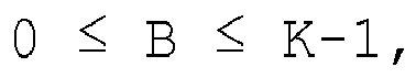
et
la commande de permutation (207) étant destinée à changer le motif de liaison (501) fourni au réseau (601 ; 602) après un nombre prédéterminé de cycles d'horloge. - Circuit selon la revendication 1, caractérisé en ce que la commande de permutation (207) comprend une mémoire (702, 703, 704, 705, 706, 707) pour stocker une pluralité de motifs de liaison (501), la commande de permutation (207) comprenant en outre une commande d'adresse (701) électriquement connectée à la mémoire (702, 703, 704, 705, 706, 707) pour sélectionner un des motifs de liaison (501), la mémoire (702, 703, 704, 705, 706, 707) étant reliée au réseau (601, 602) par une connexion électrique (311) pour émettre le motif de liaison sélectionné au réseau (602).
- Circuit selon la revendication 1, caractérisé en ce que la commande de permutation (207) comprend un registre de décalage linéaire (752), au moins deux étages du registre de décalage sont exploités et connectés à un circuit XOR (753) pour modulo-deux ajoutant les bits exploités et calculant une entrée pour le registre de décalage linéaire.
- Circuit selon l'une des revendications 1 à 3, caractérisé en ce que le réseau est un demi réseau Benes (602).
- Circuit de désentrelacement comprenant
un dispositif de désembrouillage (300 ; 302) pour recevoir un premier flux parallèle de symboles numériques à une cadence d'horloge, le premier flux parallèle (302) ayant une largeur d'un premier nombre de symboles, K,
le dispositif de désembrouillage comprenant un réseau Benes ou un demi réseau Benes (601 ; 602) pour échanger la position d'au moins la moitié des symboles numériques fournis par le premier flux parallèle contre la position d'autres symboles du premier flux parallèle et fournir un premier nombre de symboles numériques échangés, et
une commande de permutation (307) électriquement connectée au dispositif de désembrouillage (303), la commande de permutation (307) étant destinée à fournir des motifs de liaison (501) au réseau (601 ; 602), chaque motif de liaison (501) définissant l'échange des symboles numériques fournis par le premier flux parallèle, et
un dispositif de désentrelacement (305) pour recevoir un premier nombre de symboles numériques échangés et pour émettre un second flux parallèle (314) de symboles numériques ayant la largeur du premier nombre de symboles numériques K,
caractérisé en ce que
le dispositif de désentrelacement comprend K registres de décalage qui comprennent un index B correspondant pour symbole B et qui attribuent un décalage (K-1-B)T au symbole B, T étant l'inverse de la cadence d'horloge ou un multiple de l'inverse de la cadence d'horloge, et
et
la commande de permutation (307) étant destinée à changer le motif de liaison (501) fourni au réseau (601 ; 602) après un nombre prédéterminé de cycles d'horloge. - Circuit selon la revendication 5, caractérisé en ce que la commande de permutation (307) comprend une mémoire (702, 703, 704, 705, 706, 707) pour stocker une pluralité de motifs de liaison (501), la commande de permutation (307) comprenant en outre une commande d'adresse (701) électriquement connectée à la mémoire (702, 703, 704, 705, 706, 707) pour sélectionner un des motifs de liaison (501), la mémoire (702, 703, 704, 705, 706, 707) étant reliée au réseau (601, 602) par une connexion électrique (311) pour émettre le motif de liaison sélectionné au réseau (602).
- Circuit selon la revendication 5, caractérisé en ce que la commande de permutation (307) comprend un registre de décalage linéaire (752), au moins deux étages du registre de décalage sont exploités et connectés à un circuit XOR (753) pour modulo-deux ajoutant les bits exploités et calculant une entrée pour le registre de décalage linéaire.
- Circuit selon l'une des revendications 5 à 7, caractérisé en ce que le réseau est un demi réseau Benes (602).
- Circuit de réception comprenant
un égaliseur (27) comportant une entrée et une sortie, l'entrée de l'égaliseur (27) pour recevoir un flux de symboles (28) et la sortie de l'égaliseur (27) pour émettre un flux de symboles (26), et
un décorrélateur d'erreur (25) comprenant une entrée et une sortie, l'entrée du décorrélateur d'erreur (25) étant électriquement connectée à la sortie de l'égaliseur (27), le décorrélateur d'erreur (25) comprenant en outre un circuit de désentrelacement selon l'une des revendications 5 à 8. - Circuit de réception comprenant
un décorrélateur d'erreur (25) comprenant une entrée et une sortie, l'entrée pour faire entrer un flux de symboles réarrangés reçu (26), le décorrélateur d'erreur (25) étant conçu pour changer les positions des symboles à l'intérieur du flux de symboles réarrangés reçu (26), le décorrélateur d'erreur (25) pour émettre un flux de symboles encadré (23) comprenant des symboles de cadrage et les symboles codés, le décorrélateur d'erreur (25) comprenant un circuit de désentrelacement selon l'une des revendications 5 à 8, le circuit de réception comprenant en outre
un circuit FEC (22) ayant une entrée pour faire entrer un flux de symboles (23) comprenant des symboles codés, l'entrée du circuit FEC (22) étant électriquement connectée à la sortie du décorrélateur d'erreur (25), le circuit FEC (22) ayant une sortie pour émettre un flux de symboles de charge utile, le circuit FEC (22) étant conçu pour récupérer les symboles de charge utile des symboles codés. - Circuit d'émission comprenant
un circuit FEC (12) ayant une entrée pour faire entrer un flux de symboles de charge utile (11) comprenant des symboles de charge utile, le circuit FEC (12) ayant une sortie, le circuit FEC (12) étant conçu pour calculer des symboles codés en appliquant un code FEC au symboles de charge utile, le circuit FEC (12) étant conçu de plus pour émettre un flux de symboles encadré comprenant des symboles de cadrage et des symboles codés, et
un bloc de réorganisation (15) ayant une entrée et une sortie, l'entrée du bloc de réorganisation (15) étant connectée à la sortie du circuit FEC (12), le bloc de réorganisation (15) étant conçu pour changer les positions des symboles entrés par l'entrée du bloc de réorganisation (15), comprenant par cela un flux de symboles réorganisé (16), le bloc de réorganisation (15) étant conçu en outre pour émettre le flux de symboles réorganisé (16) à la sortie du bloc de réorganisation (15), le bloc de réorganisation (15) comprenant un circuit d'entrelacement selon l'une des revendications 1 à 4. - Procédé destiné à être utilisé dans un circuit d'entrelacement, comprenant
recevoir d'une entrée (13) un premier flux parallèle de symboles numériques à une cadence d'horloge, le premier flux parallèle ayant une largeur d'un premier nombre de symboles, K, et émettre un second flux parallèle (204) de symboles numériques ayant la largeur du premier nombre de symboles numériques K,
échanger, en utilisant un réseau Benes ou un demi réseau Benes, la position d'au moins la moitié des symboles numériques fournis par le second flux parallèle contre la position d'autres symboles du second flux parallèle et fournir à la sortie (16) un premier nombre de symboles numériques échangés en parallèle, et
fournir des motifs de liaison (501), en utilisant une commande de permutation, chaque motif de liaison définissant l'échange du second flux parallèle de symboles numériques,
caractérisé en ce que le procédé comprend en outre attribuer un décalage BT au symbole numérique B dans le premier flux, T étant l'inverse de la cadence d'horloge ou un multiple de l'inverse de la cadence d'horloge, et
pour fournir le second flux parallèle, et
changer le motif de liaison (501) après un nombre prédéterminé de cycles d'horloge. - Procédé destiné à être utilisé dans un circuit de désentrelacement, comprenant
recevoir un premier flux parallèle de symboles numériques à une cadence d'horloge, le premier flux parallèle (302) ayant une largeur d'un premier nombre de symboles, K,
échanger, en utilisant un réseau Benes ou un demi réseau Benes, la position d'au moins la moitié des symboles numériques fournis par le premier flux parallèle contre la position d'autres symboles du premier flux parallèle et fournir un premier nombre de symboles numériques échangés, et
fournir, en utilisant une commande de permutation (501), des motifs de liaison (501), chaque motif de liaison (501) définissant l'échange des symboles numériques fournis par le premier flux parallèle, et
caractérisé en ce que le procédé comprend en outre attribuer un décalage (K-1-B)T au symbole B dans le premier nombre de symboles numériques échangés, T étant l'inverse de la cadence d'horloge ou un multiple de l'inverse de la cadence d'horloge, et
et
fournir un second flux parallèle (314) de symboles numériques ayant la largeur du premier nombre de symboles numériques K, et
la commande de permutation (307) étant conçue pour changer le motif de liaison (501) après un nombre prédéterminé de cycles d'horloge.
Priority Applications (2)
| Application Number | Priority Date | Filing Date | Title |
|---|---|---|---|
| EP11008793.9A EP2437398B1 (fr) | 2007-10-15 | 2008-10-10 | Récepteur, circuit d'entrelacement et de désentrelacement et procédé |
| EP08838908.5A EP2097983B1 (fr) | 2007-10-15 | 2008-10-10 | Récepteur, circuit et procédé d'entrelacement et de désentrelacement |
Applications Claiming Priority (3)
| Application Number | Priority Date | Filing Date | Title |
|---|---|---|---|
| EP07118489A EP2051387A1 (fr) | 2007-10-15 | 2007-10-15 | Récepteur, circuit d'entrelacement et de désentrelacement et procédé |
| EP08838908.5A EP2097983B1 (fr) | 2007-10-15 | 2008-10-10 | Récepteur, circuit et procédé d'entrelacement et de désentrelacement |
| PCT/EP2008/063631 WO2009050121A1 (fr) | 2007-10-15 | 2008-10-10 | Récepteur, circuit et procédé d'entrelacement et de désentrelacement |
Related Child Applications (2)
| Application Number | Title | Priority Date | Filing Date |
|---|---|---|---|
| EP11008793.9A Division-Into EP2437398B1 (fr) | 2007-10-15 | 2008-10-10 | Récepteur, circuit d'entrelacement et de désentrelacement et procédé |
| EP11008793.9A Division EP2437398B1 (fr) | 2007-10-15 | 2008-10-10 | Récepteur, circuit d'entrelacement et de désentrelacement et procédé |
Publications (2)
| Publication Number | Publication Date |
|---|---|
| EP2097983A1 EP2097983A1 (fr) | 2009-09-09 |
| EP2097983B1 true EP2097983B1 (fr) | 2016-01-06 |
Family
ID=39326955
Family Applications (3)
| Application Number | Title | Priority Date | Filing Date |
|---|---|---|---|
| EP07118489A Withdrawn EP2051387A1 (fr) | 2007-10-15 | 2007-10-15 | Récepteur, circuit d'entrelacement et de désentrelacement et procédé |
| EP11008793.9A Not-in-force EP2437398B1 (fr) | 2007-10-15 | 2008-10-10 | Récepteur, circuit d'entrelacement et de désentrelacement et procédé |
| EP08838908.5A Not-in-force EP2097983B1 (fr) | 2007-10-15 | 2008-10-10 | Récepteur, circuit et procédé d'entrelacement et de désentrelacement |
Family Applications Before (2)
| Application Number | Title | Priority Date | Filing Date |
|---|---|---|---|
| EP07118489A Withdrawn EP2051387A1 (fr) | 2007-10-15 | 2007-10-15 | Récepteur, circuit d'entrelacement et de désentrelacement et procédé |
| EP11008793.9A Not-in-force EP2437398B1 (fr) | 2007-10-15 | 2008-10-10 | Récepteur, circuit d'entrelacement et de désentrelacement et procédé |
Country Status (4)
| Country | Link |
|---|---|
| US (2) | US8555132B2 (fr) |
| EP (3) | EP2051387A1 (fr) |
| JP (1) | JP5464752B2 (fr) |
| WO (1) | WO2009050121A1 (fr) |
Families Citing this family (20)
| Publication number | Priority date | Publication date | Assignee | Title |
|---|---|---|---|---|
| EP2051387A1 (fr) | 2007-10-15 | 2009-04-22 | CoreOptics, Inc., c/o The Corporation Trust Center | Récepteur, circuit d'entrelacement et de désentrelacement et procédé |
| EP2452484A1 (fr) * | 2009-07-09 | 2012-05-16 | Georgia Tech Research Corporation | Systèmes et procédés pour assurer la sécurité d'une couche physique |
| US8302043B2 (en) * | 2009-09-17 | 2012-10-30 | International Business Machines Corporation | Verification of logic circuit designs using dynamic clock gating |
| US8718491B2 (en) * | 2009-10-29 | 2014-05-06 | Ciena Corporation | Soft decoding of data in a coherent optical receiver |
| US8565271B2 (en) * | 2011-04-01 | 2013-10-22 | Opnext Subsystems, Inc. | Multiplexer lane alignment for high-speed data systems |
| US8601340B2 (en) | 2011-07-25 | 2013-12-03 | Cortina Systems, Inc. | Time varying data permutation apparatus and methods |
| US9575834B2 (en) * | 2014-05-16 | 2017-02-21 | International Business Machines Corporation | Detecting single event upsets and stuck-at faults in RAM-based data path controllers |
| US9560427B2 (en) * | 2014-05-28 | 2017-01-31 | Huawei Technologies Co., Ltd. | Scalable silicon photonic switching architectures for optical networks |
| EP4557209A3 (fr) | 2015-06-10 | 2025-08-13 | Mobileye Vision Technologies Ltd. | Processeur d'images et procédés de traitement d'une image |
| US11178072B2 (en) | 2015-06-10 | 2021-11-16 | Mobileye Vision Technologies Ltd. | Image processor and methods for processing an image |
| US10469199B2 (en) * | 2016-09-09 | 2019-11-05 | Viavi Solutions Inc. | Forward error correction with optical and electrical transponder |
| US9998146B2 (en) * | 2016-10-28 | 2018-06-12 | Inphi Corporation | Forward error correction (FEC) emulator |
| WO2018187902A1 (fr) | 2017-04-10 | 2018-10-18 | Qualcomm Incorporated | Conception d'entrelaceur efficace de codes polaires |
| WO2019116106A2 (fr) * | 2017-12-14 | 2019-06-20 | Mobileye Vision Technologies Ltd. | Processeur d'image, et procédés permettant de traiter une image |
| CN110118598B (zh) * | 2018-02-07 | 2024-07-02 | 科大国盾量子技术股份有限公司 | 用于雪崩光电二极管的延时电路及集成单光子检测电路 |
| US10216567B1 (en) * | 2018-08-22 | 2019-02-26 | Avago Technologies International Sales Pte. Limited | Direct parity encoder |
| RU2718579C1 (ru) * | 2019-05-20 | 2020-04-08 | Антон Юрьевич Баринов | Быстрый псевдослучайный перемежитель |
| FR3103070B1 (fr) * | 2019-11-13 | 2024-03-22 | Univ Grenoble Alpes | Procédé de synchronisation d’un système de communication basé sur la retransmission de données |
| US11748195B2 (en) * | 2022-01-05 | 2023-09-05 | International Business Machines Corporation | Detect multifold disturbance and minimize read-disturb errors in NAND flash |
| CN114430305B (zh) * | 2022-03-02 | 2023-06-09 | 烽火通信科技股份有限公司 | 一种细粒度帧的定帧方法和系统 |
Citations (2)
| Publication number | Priority date | Publication date | Assignee | Title |
|---|---|---|---|---|
| EP1265411A1 (fr) * | 2001-06-08 | 2002-12-11 | Sony International (Europe) GmbH | Systeme a porteuses multiples avec entrelacement au niveau du bit adaptive |
| WO2006082923A1 (fr) * | 2005-02-03 | 2006-08-10 | Matsushita Electric Industrial Co., Ltd. | Entrelaceur parallele, desentrelaceur parallele et procede d'entrelacement |
Family Cites Families (38)
| Publication number | Priority date | Publication date | Assignee | Title |
|---|---|---|---|---|
| GB2103053A (en) | 1981-06-02 | 1983-02-09 | British Broadcasting Corp | Improvements relating to transmission of data in blocks |
| US4559625A (en) * | 1983-07-28 | 1985-12-17 | Cyclotomics, Inc. | Interleavers for digital communications |
| US4547887A (en) * | 1983-11-30 | 1985-10-15 | The United States Of America As Represented By The Secretary Of The Army | Pseudo-random convolutional interleaving |
| JPH063589B2 (ja) * | 1987-10-29 | 1994-01-12 | インターナシヨナル・ビジネス・マシーンズ・コーポレーシヨン | アドレス置換装置 |
| JPH0326337A (ja) | 1989-06-21 | 1991-02-04 | Tosoh Corp | 異性化用触媒 |
| JPH03262337A (ja) * | 1990-03-09 | 1991-11-22 | Otc Ltd | アダプティブイコライザ及びデジタルデータ補間法 |
| JPH04220030A (ja) * | 1990-12-19 | 1992-08-11 | Alpine Electron Inc | デ−タ通信方式 |
| JP2755067B2 (ja) * | 1992-09-25 | 1998-05-20 | 日本電気株式会社 | フレーム同期回路 |
| US5729559A (en) * | 1995-03-27 | 1998-03-17 | Motorola, Inc. | Method and apparatus for correcting errors using multiple estimates |
| JPH08287617A (ja) | 1995-04-14 | 1996-11-01 | Toshiba Corp | データ伝送方法、データ伝送・記録装置、データ再生装置及び記録媒体 |
| JPH08331553A (ja) * | 1995-05-31 | 1996-12-13 | Alpine Electron Inc | Bsチューナの音声信号処理装置 |
| US5734676A (en) * | 1996-05-24 | 1998-03-31 | International Business Machines Corporation | Apparatus, method and article of manufacture for carrier frequency compensation in a FM radio receiver |
| US6018523A (en) * | 1997-10-22 | 2000-01-25 | Lucent Technologies, Inc. | Switching networks having improved layouts |
| JP4533472B2 (ja) * | 1998-03-19 | 2010-09-01 | 富士通株式会社 | 光増幅装置および光増幅装置による光出力制御方法ならびに光伝送装置 |
| JP2000165325A (ja) * | 1998-11-30 | 2000-06-16 | Nec Corp | 光通信装置の送信出力制御方式 |
| US6366624B1 (en) * | 1998-11-30 | 2002-04-02 | Ericsson Inc. | Systems and methods for receiving a modulated signal containing encoded and unencoded bits using multi-pass demodulation |
| US6154452A (en) | 1999-05-26 | 2000-11-28 | Xm Satellite Radio Inc. | Method and apparatus for continuous cross-channel interleaving |
| JP4207329B2 (ja) * | 1999-09-20 | 2009-01-14 | 富士通株式会社 | フレーム同期回路 |
| JP3770767B2 (ja) * | 2000-02-17 | 2006-04-26 | 株式会社日立製作所 | トランスポンダ、波長多重伝送装置、波長多重伝送システムおよび情報通信装置 |
| US6971057B1 (en) * | 2000-02-25 | 2005-11-29 | Globespanvirata, Inc. | System and method for efficient convolutional interleaving/de-interleaving |
| US6606718B1 (en) * | 2000-05-11 | 2003-08-12 | Agere Systems Inc. | Product code with interleaving to enhance error detection and correction |
| JP2001326671A (ja) * | 2000-05-17 | 2001-11-22 | Nec Corp | 光通信装置及びそれを使用する車両間lanシステム |
| JP3668673B2 (ja) * | 2000-06-09 | 2005-07-06 | 株式会社日立コミュニケーションテクノロジー | エラー訂正符号の構成方法、復号方法、伝送装置、ネットワーク |
| KR100889465B1 (ko) * | 2000-07-04 | 2009-03-20 | 코닌클리케 필립스 일렉트로닉스 엔.브이. | 대칭-키 암호들을 위한 치환-박스 |
| US6738392B1 (en) * | 2000-09-27 | 2004-05-18 | Cisco Technology, Inc. | Method and apparatus of framing high-speed signals |
| US6873613B1 (en) * | 2000-10-16 | 2005-03-29 | Ericsson Inc. | Methods for wirelessly communicating time division multiple access (TDMA) data using adaptive multiplexing and coding |
| JP2002150698A (ja) * | 2000-11-06 | 2002-05-24 | Pioneer Electronic Corp | 情報記録方法、情報記録装置、情報再生方法及び情報再生装置 |
| EP1303052B1 (fr) * | 2001-10-10 | 2005-08-03 | Matsushita Electric Industrial Co., Ltd. | Modification des motifs d'un entrelaceur |
| US20030072328A1 (en) * | 2001-10-15 | 2003-04-17 | Echartea Jesus Palomino | Framing data in a control circuit |
| US7593411B2 (en) * | 2002-02-21 | 2009-09-22 | Pmc-Sierra, Inc. | Bus interface for transfer of multiple SONET/SDH rates over a serial backplane |
| EP1494413A1 (fr) | 2003-07-02 | 2005-01-05 | CoreOptics, Inc., c/o The Corporation Trust Center | Estimation de canal et de séquence pour la réception de signaux optiques |
| JP2005110228A (ja) * | 2003-09-10 | 2005-04-21 | Matsushita Electric Ind Co Ltd | セキュア通信方法および送信装置、受信装置 |
| JP4379251B2 (ja) | 2004-08-02 | 2009-12-09 | トヨタ自動車株式会社 | 内燃機関の制御装置および制御方法 |
| TWI290426B (en) * | 2005-02-03 | 2007-11-21 | Sanyo Electric Co | Encryption processing circuit |
| US7657818B2 (en) * | 2005-06-22 | 2010-02-02 | Adaptive Spectrum And Signal Alignment, Inc. | Dynamic minimum-memory interleaving |
| KR100797176B1 (ko) * | 2005-10-21 | 2008-01-23 | 삼성전자주식회사 | 디지털 방송 시스템 및 그 방법 |
| JP4317860B2 (ja) * | 2006-08-30 | 2009-08-19 | 株式会社日立コミュニケーションテクノロジー | 光集線装置および光加入者装置 |
| EP2051387A1 (fr) | 2007-10-15 | 2009-04-22 | CoreOptics, Inc., c/o The Corporation Trust Center | Récepteur, circuit d'entrelacement et de désentrelacement et procédé |
-
2007
- 2007-10-15 EP EP07118489A patent/EP2051387A1/fr not_active Withdrawn
- 2007-10-25 US US11/924,397 patent/US8555132B2/en not_active Expired - Fee Related
-
2008
- 2008-10-10 EP EP11008793.9A patent/EP2437398B1/fr not_active Not-in-force
- 2008-10-10 WO PCT/EP2008/063631 patent/WO2009050121A1/fr not_active Ceased
- 2008-10-10 EP EP08838908.5A patent/EP2097983B1/fr not_active Not-in-force
- 2008-10-10 JP JP2010528413A patent/JP5464752B2/ja not_active Expired - Fee Related
-
2013
- 2013-08-02 US US13/957,639 patent/US8874988B2/en active Active
Patent Citations (3)
| Publication number | Priority date | Publication date | Assignee | Title |
|---|---|---|---|---|
| EP1265411A1 (fr) * | 2001-06-08 | 2002-12-11 | Sony International (Europe) GmbH | Systeme a porteuses multiples avec entrelacement au niveau du bit adaptive |
| WO2006082923A1 (fr) * | 2005-02-03 | 2006-08-10 | Matsushita Electric Industrial Co., Ltd. | Entrelaceur parallele, desentrelaceur parallele et procede d'entrelacement |
| EP1850486A1 (fr) * | 2005-02-03 | 2007-10-31 | Matsushita Electric Industrial Co., Ltd. | Entrelaceur parallele, desentrelaceur parallele et procede d'entrelacement |
Non-Patent Citations (1)
| Title |
|---|
| YUAN J ET AL: "DESIGN OF CYCLIC SHIFT INTERLEAVERS FOR TURBO CODES//STRUCTURE D'ENTRELACEMENTS A DECALAGE CYCLIQUE POUR LES TURBOCODES", ANNALES DES TELECOMMUNICATIONS - ANNALS OF TELECOMMUNICATIONS, GET LAVOISIER, PARIS, FR, vol. 56, no. 7/08, 1 July 2001 (2001-07-01), pages 384 - 393, XP001100319, ISSN: 0003-4347 * |
Also Published As
| Publication number | Publication date |
|---|---|
| US8874988B2 (en) | 2014-10-28 |
| US8555132B2 (en) | 2013-10-08 |
| JP2011501491A (ja) | 2011-01-06 |
| WO2009050121A1 (fr) | 2009-04-23 |
| EP2437398A3 (fr) | 2012-05-09 |
| US20090100314A1 (en) | 2009-04-16 |
| US20130318417A1 (en) | 2013-11-28 |
| EP2051387A1 (fr) | 2009-04-22 |
| JP5464752B2 (ja) | 2014-04-09 |
| EP2097983A1 (fr) | 2009-09-09 |
| EP2437398B1 (fr) | 2015-03-18 |
| EP2437398A2 (fr) | 2012-04-04 |
Similar Documents
| Publication | Publication Date | Title |
|---|---|---|
| EP2097983B1 (fr) | Récepteur, circuit et procédé d'entrelacement et de désentrelacement | |
| JP3549788B2 (ja) | 多段符号化方法、多段復号方法、多段符号化装置、多段復号装置およびこれらを用いた情報伝送システム | |
| CA2098772C (fr) | Methode et appareil pour la transmission de donnees imbriquees | |
| US7284184B2 (en) | Forward error correction scheme compatible with the bit error spreading of a scrambler | |
| US7103830B1 (en) | DC balanced error correction coding | |
| US4312070A (en) | Digital encoder-decoder | |
| US5519734A (en) | Synchronization arrangement for decoder-de-interleaver | |
| US6516436B1 (en) | Error control coding for transmission equipment protection | |
| DK155399B (da) | Apparat og fremgangsmaade til datatransmission med fejlkorrigeringsmulighed, samt dekoder til brug i forbindelse med fremgangsmaaden og/eller apparatet. | |
| US8458560B2 (en) | Systems and methods for efficient parallel implementation of burst error correction codes | |
| EP2831999B1 (fr) | Codage parallèle pour code de bloc linéaire non binaire | |
| US4592054A (en) | Decoder with code error correcting function | |
| WO2009060185A2 (fr) | Entrelacement et désentrelacement d'un flux de données reçu dans des trames successives | |
| EP1217748A2 (fr) | Décodeur en bande pour correcteur d'erreur sans voie de retour (FEC) pour SONET | |
| EP1215837A2 (fr) | Codeur intraband a correction d'erreurs en avant pour SONET | |
| US7447982B1 (en) | BCH forward error correction decoder | |
| US20040117711A1 (en) | Method for improving the performance of 3-dimensional concatenated product codes | |
| EP1529344A2 (fr) | Procede de premier entrelacement d'un emetteur a deux entrelaceurs | |
| US7502390B2 (en) | Optimized interleaver and/or deinterleaver design | |
| US7225306B2 (en) | Efficient address generation for Forney's modular periodic interleavers | |
| EP1217750A2 (fr) | Dispositif pour élever au carré sur GF(2M), optimisé, avec entée parallèle, sortie parallèle pour un décodeur d'erreur sans voie de retour (FEC) | |
| JP3173713B2 (ja) | エラー訂正符号化方法および送受信装置 | |
| Gorshe | Concurrent error detection | |
| Olcayto et al. | Split-syndrome burst error correcting codes for one-dimensional channels | |
| Lewis | Burst and compound error correction with cyclic codes. |
Legal Events
| Date | Code | Title | Description |
|---|---|---|---|
| PUAI | Public reference made under article 153(3) epc to a published international application that has entered the european phase |
Free format text: ORIGINAL CODE: 0009012 |
|
| 17P | Request for examination filed |
Effective date: 20090708 |
|
| AK | Designated contracting states |
Kind code of ref document: A1 Designated state(s): AT BE BG CH CY CZ DE DK EE ES FI FR GB GR HR HU IE IS IT LI LT LU LV MC MT NL NO PL PT RO SE SI SK TR |
|
| 17Q | First examination report despatched |
Effective date: 20091106 |
|
| RIN1 | Information on inventor provided before grant (corrected) |
Inventor name: DANNINGER, MARKUS Inventor name: PRESSLEIN, PAUL Inventor name: KUPFER, THEODOR |
|
| DAX | Request for extension of the european patent (deleted) | ||
| RAP1 | Party data changed (applicant data changed or rights of an application transferred) |
Owner name: CISCO TECHNOLOGY, INC. |
|
| REG | Reference to a national code |
Ref country code: DE Ref legal event code: R079 Ref document number: 602008041928 Country of ref document: DE Free format text: PREVIOUS MAIN CLASS: H03M0013270000 Ipc: H03M0013150000 |
|
| GRAP | Despatch of communication of intention to grant a patent |
Free format text: ORIGINAL CODE: EPIDOSNIGR1 |
|
| RIC1 | Information provided on ipc code assigned before grant |
Ipc: H03M 13/15 20060101AFI20150629BHEP Ipc: H03M 13/27 20060101ALI20150629BHEP Ipc: H03M 13/29 20060101ALI20150629BHEP Ipc: H04L 1/00 20060101ALI20150629BHEP Ipc: H04J 3/06 20060101ALI20150629BHEP |
|
| INTG | Intention to grant announced |
Effective date: 20150724 |
|
| GRAS | Grant fee paid |
Free format text: ORIGINAL CODE: EPIDOSNIGR3 |
|
| GRAA | (expected) grant |
Free format text: ORIGINAL CODE: 0009210 |
|
| AK | Designated contracting states |
Kind code of ref document: B1 Designated state(s): AT BE BG CH CY CZ DE DK EE ES FI FR GB GR HR HU IE IS IT LI LT LU LV MC MT NL NO PL PT RO SE SI SK TR |
|
| REG | Reference to a national code |
Ref country code: GB Ref legal event code: FG4D |
|
| REG | Reference to a national code |
Ref country code: CH Ref legal event code: EP |
|
| REG | Reference to a national code |
Ref country code: IE Ref legal event code: FG4D |
|
| REG | Reference to a national code |
Ref country code: AT Ref legal event code: REF Ref document number: 769638 Country of ref document: AT Kind code of ref document: T Effective date: 20160215 |
|
| REG | Reference to a national code |
Ref country code: DE Ref legal event code: R096 Ref document number: 602008041928 Country of ref document: DE |
|
| REG | Reference to a national code |
Ref country code: LT Ref legal event code: MG4D |
|
| REG | Reference to a national code |
Ref country code: NL Ref legal event code: MP Effective date: 20160106 |
|
| REG | Reference to a national code |
Ref country code: AT Ref legal event code: MK05 Ref document number: 769638 Country of ref document: AT Kind code of ref document: T Effective date: 20160106 |
|
| PG25 | Lapsed in a contracting state [announced via postgrant information from national office to epo] |
Ref country code: NL Free format text: LAPSE BECAUSE OF FAILURE TO SUBMIT A TRANSLATION OF THE DESCRIPTION OR TO PAY THE FEE WITHIN THE PRESCRIBED TIME-LIMIT Effective date: 20160106 |
|
| PG25 | Lapsed in a contracting state [announced via postgrant information from national office to epo] |
Ref country code: GR Free format text: LAPSE BECAUSE OF FAILURE TO SUBMIT A TRANSLATION OF THE DESCRIPTION OR TO PAY THE FEE WITHIN THE PRESCRIBED TIME-LIMIT Effective date: 20160407 Ref country code: HR Free format text: LAPSE BECAUSE OF FAILURE TO SUBMIT A TRANSLATION OF THE DESCRIPTION OR TO PAY THE FEE WITHIN THE PRESCRIBED TIME-LIMIT Effective date: 20160106 Ref country code: ES Free format text: LAPSE BECAUSE OF FAILURE TO SUBMIT A TRANSLATION OF THE DESCRIPTION OR TO PAY THE FEE WITHIN THE PRESCRIBED TIME-LIMIT Effective date: 20160106 Ref country code: FI Free format text: LAPSE BECAUSE OF FAILURE TO SUBMIT A TRANSLATION OF THE DESCRIPTION OR TO PAY THE FEE WITHIN THE PRESCRIBED TIME-LIMIT Effective date: 20160106 Ref country code: NO Free format text: LAPSE BECAUSE OF FAILURE TO SUBMIT A TRANSLATION OF THE DESCRIPTION OR TO PAY THE FEE WITHIN THE PRESCRIBED TIME-LIMIT Effective date: 20160406 Ref country code: IT Free format text: LAPSE BECAUSE OF FAILURE TO SUBMIT A TRANSLATION OF THE DESCRIPTION OR TO PAY THE FEE WITHIN THE PRESCRIBED TIME-LIMIT Effective date: 20160106 |
|
| PG25 | Lapsed in a contracting state [announced via postgrant information from national office to epo] |
Ref country code: LT Free format text: LAPSE BECAUSE OF FAILURE TO SUBMIT A TRANSLATION OF THE DESCRIPTION OR TO PAY THE FEE WITHIN THE PRESCRIBED TIME-LIMIT Effective date: 20160106 Ref country code: AT Free format text: LAPSE BECAUSE OF FAILURE TO SUBMIT A TRANSLATION OF THE DESCRIPTION OR TO PAY THE FEE WITHIN THE PRESCRIBED TIME-LIMIT Effective date: 20160106 Ref country code: IS Free format text: LAPSE BECAUSE OF FAILURE TO SUBMIT A TRANSLATION OF THE DESCRIPTION OR TO PAY THE FEE WITHIN THE PRESCRIBED TIME-LIMIT Effective date: 20160506 Ref country code: SE Free format text: LAPSE BECAUSE OF FAILURE TO SUBMIT A TRANSLATION OF THE DESCRIPTION OR TO PAY THE FEE WITHIN THE PRESCRIBED TIME-LIMIT Effective date: 20160106 Ref country code: PL Free format text: LAPSE BECAUSE OF FAILURE TO SUBMIT A TRANSLATION OF THE DESCRIPTION OR TO PAY THE FEE WITHIN THE PRESCRIBED TIME-LIMIT Effective date: 20160106 Ref country code: PT Free format text: LAPSE BECAUSE OF FAILURE TO SUBMIT A TRANSLATION OF THE DESCRIPTION OR TO PAY THE FEE WITHIN THE PRESCRIBED TIME-LIMIT Effective date: 20160506 Ref country code: LV Free format text: LAPSE BECAUSE OF FAILURE TO SUBMIT A TRANSLATION OF THE DESCRIPTION OR TO PAY THE FEE WITHIN THE PRESCRIBED TIME-LIMIT Effective date: 20160106 |
|
| REG | Reference to a national code |
Ref country code: DE Ref legal event code: R097 Ref document number: 602008041928 Country of ref document: DE |
|
| REG | Reference to a national code |
Ref country code: FR Ref legal event code: PLFP Year of fee payment: 9 |
|
| PG25 | Lapsed in a contracting state [announced via postgrant information from national office to epo] |
Ref country code: DK Free format text: LAPSE BECAUSE OF FAILURE TO SUBMIT A TRANSLATION OF THE DESCRIPTION OR TO PAY THE FEE WITHIN THE PRESCRIBED TIME-LIMIT Effective date: 20160106 Ref country code: EE Free format text: LAPSE BECAUSE OF FAILURE TO SUBMIT A TRANSLATION OF THE DESCRIPTION OR TO PAY THE FEE WITHIN THE PRESCRIBED TIME-LIMIT Effective date: 20160106 |
|
| PLBE | No opposition filed within time limit |
Free format text: ORIGINAL CODE: 0009261 |
|
| STAA | Information on the status of an ep patent application or granted ep patent |
Free format text: STATUS: NO OPPOSITION FILED WITHIN TIME LIMIT |
|
| PG25 | Lapsed in a contracting state [announced via postgrant information from national office to epo] |
Ref country code: SK Free format text: LAPSE BECAUSE OF FAILURE TO SUBMIT A TRANSLATION OF THE DESCRIPTION OR TO PAY THE FEE WITHIN THE PRESCRIBED TIME-LIMIT Effective date: 20160106 Ref country code: CZ Free format text: LAPSE BECAUSE OF FAILURE TO SUBMIT A TRANSLATION OF THE DESCRIPTION OR TO PAY THE FEE WITHIN THE PRESCRIBED TIME-LIMIT Effective date: 20160106 Ref country code: RO Free format text: LAPSE BECAUSE OF FAILURE TO SUBMIT A TRANSLATION OF THE DESCRIPTION OR TO PAY THE FEE WITHIN THE PRESCRIBED TIME-LIMIT Effective date: 20160106 |
|
| 26N | No opposition filed |
Effective date: 20161007 |
|
| PG25 | Lapsed in a contracting state [announced via postgrant information from national office to epo] |
Ref country code: BE Free format text: LAPSE BECAUSE OF FAILURE TO SUBMIT A TRANSLATION OF THE DESCRIPTION OR TO PAY THE FEE WITHIN THE PRESCRIBED TIME-LIMIT Effective date: 20160106 |
|
| PG25 | Lapsed in a contracting state [announced via postgrant information from national office to epo] |
Ref country code: SI Free format text: LAPSE BECAUSE OF FAILURE TO SUBMIT A TRANSLATION OF THE DESCRIPTION OR TO PAY THE FEE WITHIN THE PRESCRIBED TIME-LIMIT Effective date: 20160106 Ref country code: BG Free format text: LAPSE BECAUSE OF FAILURE TO SUBMIT A TRANSLATION OF THE DESCRIPTION OR TO PAY THE FEE WITHIN THE PRESCRIBED TIME-LIMIT Effective date: 20160406 |
|
| REG | Reference to a national code |
Ref country code: CH Ref legal event code: PL |
|
| REG | Reference to a national code |
Ref country code: IE Ref legal event code: MM4A |
|
| PG25 | Lapsed in a contracting state [announced via postgrant information from national office to epo] |
Ref country code: LI Free format text: LAPSE BECAUSE OF NON-PAYMENT OF DUE FEES Effective date: 20161031 Ref country code: CH Free format text: LAPSE BECAUSE OF NON-PAYMENT OF DUE FEES Effective date: 20161031 |
|
| PG25 | Lapsed in a contracting state [announced via postgrant information from national office to epo] |
Ref country code: LU Free format text: LAPSE BECAUSE OF NON-PAYMENT OF DUE FEES Effective date: 20161010 |
|
| REG | Reference to a national code |
Ref country code: FR Ref legal event code: PLFP Year of fee payment: 10 |
|
| PG25 | Lapsed in a contracting state [announced via postgrant information from national office to epo] |
Ref country code: IE Free format text: LAPSE BECAUSE OF NON-PAYMENT OF DUE FEES Effective date: 20161010 |
|
| PG25 | Lapsed in a contracting state [announced via postgrant information from national office to epo] |
Ref country code: CY Free format text: LAPSE BECAUSE OF FAILURE TO SUBMIT A TRANSLATION OF THE DESCRIPTION OR TO PAY THE FEE WITHIN THE PRESCRIBED TIME-LIMIT Effective date: 20160106 Ref country code: HU Free format text: LAPSE BECAUSE OF FAILURE TO SUBMIT A TRANSLATION OF THE DESCRIPTION OR TO PAY THE FEE WITHIN THE PRESCRIBED TIME-LIMIT; INVALID AB INITIO Effective date: 20081010 |
|
| PG25 | Lapsed in a contracting state [announced via postgrant information from national office to epo] |
Ref country code: MT Free format text: LAPSE BECAUSE OF NON-PAYMENT OF DUE FEES Effective date: 20161031 Ref country code: MC Free format text: LAPSE BECAUSE OF FAILURE TO SUBMIT A TRANSLATION OF THE DESCRIPTION OR TO PAY THE FEE WITHIN THE PRESCRIBED TIME-LIMIT Effective date: 20160106 Ref country code: TR Free format text: LAPSE BECAUSE OF FAILURE TO SUBMIT A TRANSLATION OF THE DESCRIPTION OR TO PAY THE FEE WITHIN THE PRESCRIBED TIME-LIMIT Effective date: 20160106 |
|
| REG | Reference to a national code |
Ref country code: FR Ref legal event code: PLFP Year of fee payment: 11 |
|
| REG | Reference to a national code |
Ref country code: DE Ref legal event code: R082 Ref document number: 602008041928 Country of ref document: DE Representative=s name: HL KEMPNER PATENTANWAELTE, SOLICITORS (ENGLAND, DE Ref country code: DE Ref legal event code: R082 Ref document number: 602008041928 Country of ref document: DE Representative=s name: HL KEMPNER PATENTANWALT, RECHTSANWALT, SOLICIT, DE Ref country code: DE Ref legal event code: R082 Ref document number: 602008041928 Country of ref document: DE Representative=s name: HL KEMPNER PARTG MBB, DE |
|
| PGFP | Annual fee paid to national office [announced via postgrant information from national office to epo] |
Ref country code: FR Payment date: 20201026 Year of fee payment: 13 |
|
| PG25 | Lapsed in a contracting state [announced via postgrant information from national office to epo] |
Ref country code: FR Free format text: LAPSE BECAUSE OF NON-PAYMENT OF DUE FEES Effective date: 20211031 |
|
| P01 | Opt-out of the competence of the unified patent court (upc) registered |
Effective date: 20230525 |
|
| PGFP | Annual fee paid to national office [announced via postgrant information from national office to epo] |
Ref country code: GB Payment date: 20231027 Year of fee payment: 16 |
|
| PGFP | Annual fee paid to national office [announced via postgrant information from national office to epo] |
Ref country code: DE Payment date: 20231026 Year of fee payment: 16 |
|
| REG | Reference to a national code |
Ref country code: DE Ref legal event code: R119 Ref document number: 602008041928 Country of ref document: DE |
|
| GBPC | Gb: european patent ceased through non-payment of renewal fee |
Effective date: 20241010 |
|
| PG25 | Lapsed in a contracting state [announced via postgrant information from national office to epo] |
Ref country code: DE Free format text: LAPSE BECAUSE OF NON-PAYMENT OF DUE FEES Effective date: 20250501 |
|
| PG25 | Lapsed in a contracting state [announced via postgrant information from national office to epo] |
Ref country code: GB Free format text: LAPSE BECAUSE OF NON-PAYMENT OF DUE FEES Effective date: 20241010 |