EP2164174A2 - Méthode et circuit pour augmenter la tension de claquage de transitors MOS à basses températures. - Google Patents
Méthode et circuit pour augmenter la tension de claquage de transitors MOS à basses températures. Download PDFInfo
- Publication number
- EP2164174A2 EP2164174A2 EP09168721A EP09168721A EP2164174A2 EP 2164174 A2 EP2164174 A2 EP 2164174A2 EP 09168721 A EP09168721 A EP 09168721A EP 09168721 A EP09168721 A EP 09168721A EP 2164174 A2 EP2164174 A2 EP 2164174A2
- Authority
- EP
- European Patent Office
- Prior art keywords
- metal oxide
- circuit arrangement
- voltage
- oxide transistor
- transistor
- Prior art date
- Legal status (The legal status is an assumption and is not a legal conclusion. Google has not performed a legal analysis and makes no representation as to the accuracy of the status listed.)
- Withdrawn
Links
Images
Classifications
-
- H—ELECTRICITY
- H03—ELECTRONIC CIRCUITRY
- H03K—PULSE TECHNIQUE
- H03K19/00—Logic circuits, i.e. having at least two inputs acting on one output; Inverting circuits
- H03K19/003—Modifications for increasing the reliability for protection
- H03K19/00315—Modifications for increasing the reliability for protection in field-effect transistor circuits
-
- H—ELECTRICITY
- H03—ELECTRONIC CIRCUITRY
- H03K—PULSE TECHNIQUE
- H03K19/00—Logic circuits, i.e. having at least two inputs acting on one output; Inverting circuits
- H03K19/003—Modifications for increasing the reliability for protection
- H03K19/00369—Modifications for compensating variations of temperature, supply voltage or other physical parameters
- H03K19/00384—Modifications for compensating variations of temperature, supply voltage or other physical parameters in field effect transistor circuits
-
- H—ELECTRICITY
- H10—SEMICONDUCTOR DEVICES; ELECTRIC SOLID-STATE DEVICES NOT OTHERWISE PROVIDED FOR
- H10W—GENERIC PACKAGES, INTERCONNECTIONS, CONNECTORS OR OTHER CONSTRUCTIONAL DETAILS OF DEVICES COVERED BY CLASS H10
- H10W40/00—Arrangements for thermal protection or thermal control
- H10W40/10—Arrangements for heating
Definitions
- the invention relates to a method for increasing the temperature-independent dielectric strength of electronic circuit arrangements with metal oxide according to the preamble of the main claim, and of a circuit arrangement with at least one metal oxide and an elevated temperature-independent withstand voltage according to the preamble of the independent claim.
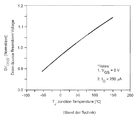
- the single FIGURE shows a graph of the normalized breakdown voltage of a metal oxide transistor according to the prior art, also abbreviated to MOSFET, plotted against the chip temperature. It can clearly be seen that the breakdown voltage of the metal oxide transistor also drops considerably as the temperature of the metal oxide transistor decreases. This raises the problem that the withstand voltage of an entire circuit including such a metal oxide transistor also decreases at low temperatures. To circumvent this problem, metal oxide transistors with higher blocking voltage have hitherto been used. However, these are considerably more expensive and have disadvantages such as higher channel resistance (RDS On ). The problem is particularly serious if, due to the boundary conditions, metal oxide transistors must be selected which exceed a voltage level due to technology.
- RDS On higher channel resistance
- the object is achieved with respect to the method according to the invention with a method for increasing the dielectric strength of an electronic circuit arrangement at low temperatures, wherein the circuit arrangement has at least one metal oxide transistor, and before applying a voltage which is in the vicinity of the breakdown voltage of the metal oxide, this is heated by suitable means to a predetermined temperature.
- the heating of the metal oxide transistor is achieved by a high current through the metal oxide transistor.
- the heating of the metal oxide transistor is accomplished by increasing the switching losses of the metal oxide transistor.
- the heating of the metal oxide transistor is accomplished by a short-term linear operation of the metal oxide transistor.
- the heating can be either time-controlled or temperature-controlled.
- the timed variant heats the metal oxide transistor for a predetermined time. It offers the advantage of a cost-effective implementation.
- the temperature controlled variant measures the temperature of the circuitry or metal oxide transistor and heats it to a predetermined temperature (e.g., 25 ° C). It offers the advantage of good temperature control of the metal oxide transistor.
- the heating is preferably accomplished only at low temperatures of the circuit or the metal oxide. This prevents overheating of the metal oxide at higher temperatures of the circuit or the metal oxide transistor.
- circuit arrangement with an increased dielectric strength at low temperatures, wherein the circuit arrangement comprises at least one metal oxide, and it has means for heating the metal oxide before it reaches a voltage in the vicinity of the reverse voltage of the metal oxide lies, touches him.
- the heating of the metal oxide transistor is achieved by a high current through the metal oxide transistor.
- the heating of the metal oxide transistor is accomplished by increasing the switching losses of the metal oxide transistor.
- the heating of the metal oxide transistor is accomplished by a short-term linear operation of the metal oxide transistor.
- the circuit arrangement preferably heats the latter only at low temperatures of the circuit arrangement or of the metal oxide transistor. This prevents overheating of the metal oxide at higher temperatures of the circuit or the metal oxide transistor.
- the heating can be either time-controlled or temperature-controlled.
- the timed variant offers the advantage of a cost-effective implementation.
- the temperature controlled version offers the advantage of a precise temperature control of the metal oxide transistor.
- the circuit arrangement preferably measures the temperature of the metal oxide transistor. Particularly preferably, the temperature of the metal oxide transistor is measured via its channel resistance. This offers the advantage of a simple and inexpensive implementation of the temperature measurement.
- the circuit arrangement is preferably designed to operate at least one gas discharge lamp, wherein it generates an intermediate circuit voltage for application to the metal oxide transistor, and heats the metal oxide transistor shortly before the start of the gas discharge lamp or at the start of the gas discharge lamp.
- just before the start means that the circuit uses the time before the lamp start in which it builds the ignition voltage for the heating of the metal oxide transistor.
- the DC link voltage is advantageously lowered during the heating phase, and the heating phase between 1s and 120s long. By lowering the DC link voltage, the metal oxide transistor is protected, and the length of the heating phase guarantees effective heating of the transistor.
- the lowering of the intermediate circuit voltage is preferably accomplished by a DC-DC converter having an adjustable output voltage, and whose output voltage is the intermediate circuit voltage. Since a DC-DC converter is used in many cases for other reasons, it is advantageous to make this existing DC-DC converter with little effort in its output voltage adjustable to adjust the DC link voltage can.
- a metal oxide transistor having no increased reverse voltage can be used.
- the latter prior to application of a voltage to the metal oxide transistor, which lies in the region of the blocking voltage of the metal oxide transistor, the latter is heated to a temperature at which it can reliably block the voltage to be applied.
- the temperature dependence of the blocking voltage of metal oxide transistors is utilized.
- the metal oxide transistor is used as a switching transistor in the inverter of an electronic control gear for gas discharge lamps.
- the inverter is often preceded by a DC-DC converter, for example, a power factor correction can perform.
- the DC-DC converter can be designed for example as a boost, Sepic or flyback converter.
- the DC-DC converter generates a regulated output voltage that is input to the inverter. This voltage is often referred to as a DC link voltage.
- the inverter can be designed as a Class-E converter, as a half-bridge inverter or as a full-bridge inverter. Accordingly, the inverter has between one and four metal oxide transistors. In such an operating device, these metal oxide transistors are often operated near the blocking voltage in continuous lamp operation.
- the lamp voltage of the gas discharge lamp to be operated is thus in the range of the blocking voltage of the metal oxide transistor.
- the electronic control gear for outdoor applications at low ambient temperatures of eg -40 ° C or even applications can be specified in cold stores, which then entail a correspondingly low temperature of the circuit or the Metalloxidtransistors, it is necessary, the or the Metalloxidtransistoren accordingly preheat so that they can lock the rapidly increasing lamp voltage of the gas discharge lamp after starting.
- the period of time in which the metal oxide transistor is preheated, and therefore in which the voltage applied to the transistor, for example the intermediate circuit voltage, is lowered, is between 1 s and 120 s.
- the metal oxide transistor can be heated by various methods. Many operating devices ignite the high-pressure discharge lamps by means of a resonance ignition, similar to the case with low-pressure discharge lamps. During this resonant phase, a high current flows through the metal oxide transistor, which can heat it up quickly and reliably. In order to optimize the heating, the metal oxide transistor may be operated in the linear region for a short period of time during the resonance ignition to accelerate the heat input to the transistor. This short period of time during which the metal oxide transistor has a higher on-resistance (R DSOn ) during which resonance is attenuated is imperceptible to the user.
- R DSOn on-resistance
- Another variant is to heat the metal oxide during the heating of the high pressure discharge lamp. Shortly after ignition, a high-pressure discharge lamp still has a rather low lamp voltage, which rises steadily during the start-up of the lamp. During this time, the metal oxide transistor can also be heated without running the risk of being destroyed by overvoltage. The heating takes place again by increased switching losses during the heating phase.
- the increased switching losses can be caused, for example, by a capacitive operation of the metal oxide transistor, or by an increase in the switching frequency, which increases the losses per unit time.
- the increase of the switching frequency has the advantage that thereby the voltage switched by the metal oxide transistor voltage can be lowered, without a fading of the arc must be feared.
- both options are combined, and the transistor is heated during the ignition of the high-pressure discharge lamp and also during the start-up of the high-pressure discharge lamp.
- the DC link voltage can be lowered by the DC-DC converter, since, as already mentioned above, the lamp voltage is correspondingly low. This ensures that the metal oxide transistor can safely block the voltage applied to it.
- One way to control the heating phases is to measure the metal oxide transistor temperature. This can be done by a temperature sensor attached to the metal oxide transistor or by means of the sheet resistance of the metal oxide transistor. The track resistance can be measured by means of a temperature-compensated measuring arrangement, and thus the chip temperature of the metal oxide transistor can be determined. The heating phases are then controlled until the transistor has reached a predetermined minimum temperature (e.g., + 25 ° C).
- a predetermined minimum temperature e.g., + 25 ° C.
- the metal oxide transistor may drop below a predetermined temperature. Then additional heating phases are to be provided even in normal operation in order to ensure safe operation of the metal oxide transistor.
- the heating phases can be implemented as described above in the operation of the high pressure discharge lamp. In this connection, a linear operation of the metal oxide transistor and / or a temporary turn-off of the zero-voltage switching (ZVS) of the metal oxide transistor or the current-free switching (ZCS) of the metal oxide transistor is preferable to the other described methods.
Landscapes
- Physics & Mathematics (AREA)
- Engineering & Computer Science (AREA)
- Computer Hardware Design (AREA)
- Computing Systems (AREA)
- General Engineering & Computer Science (AREA)
- Mathematical Physics (AREA)
- General Induction Heating (AREA)
- Circuit Arrangements For Discharge Lamps (AREA)
- Semiconductor Integrated Circuits (AREA)
- Electronic Switches (AREA)
Applications Claiming Priority (1)
| Application Number | Priority Date | Filing Date | Title |
|---|---|---|---|
| DE102008046734A DE102008046734A1 (de) | 2008-09-11 | 2008-09-11 | Verfahren und Schaltungsanordnung zur Erhöhung der Spannungsfestigkeit von Metalloxidtransistoren bei niedrigen Temperaturen |
Publications (2)
| Publication Number | Publication Date |
|---|---|
| EP2164174A2 true EP2164174A2 (fr) | 2010-03-17 |
| EP2164174A3 EP2164174A3 (fr) | 2010-05-26 |
Family
ID=41100795
Family Applications (1)
| Application Number | Title | Priority Date | Filing Date |
|---|---|---|---|
| EP09168721A Withdrawn EP2164174A3 (fr) | 2008-09-11 | 2009-08-26 | Méthode et circuit pour augmenter la tension de claquage de transitors MOS à basses températures. |
Country Status (6)
| Country | Link |
|---|---|
| US (1) | US20100060193A1 (fr) |
| EP (1) | EP2164174A3 (fr) |
| JP (1) | JP2010067974A (fr) |
| KR (1) | KR20100031088A (fr) |
| CN (1) | CN101674699B (fr) |
| DE (1) | DE102008046734A1 (fr) |
Families Citing this family (2)
| Publication number | Priority date | Publication date | Assignee | Title |
|---|---|---|---|---|
| EP2680302A1 (fr) | 2011-02-21 | 2014-01-01 | Panasonic Corporation | Circuit intégré |
| CN115461491B (zh) * | 2020-07-01 | 2024-08-23 | 应用材料公司 | 用于操作腔室的方法、用于处理基板的装置和基板处理系统 |
Citations (1)
| Publication number | Priority date | Publication date | Assignee | Title |
|---|---|---|---|---|
| WO2001087020A1 (fr) * | 2000-04-27 | 2001-11-15 | Lumion Corporation | Circuit de commande de ballast universel |
Family Cites Families (12)
| Publication number | Priority date | Publication date | Assignee | Title |
|---|---|---|---|---|
| US3337736A (en) * | 1965-06-04 | 1967-08-22 | Frutiger Peter | Photo-electric detection system with self-compensation for changes in incident light |
| JPH08306914A (ja) * | 1995-04-27 | 1996-11-22 | Nippondenso Co Ltd | 半導体装置およびその製造方法 |
| GB9513420D0 (en) * | 1995-06-30 | 1995-09-06 | Philips Electronics Uk Ltd | Power semiconductor devices |
| FR2742583B1 (fr) * | 1995-12-18 | 1998-04-24 | Sgs Thomson Microelectronics | Transistor a effet de champ a grille isolee et a canal diffuse |
| US6348808B1 (en) * | 1999-06-25 | 2002-02-19 | Lsi Logic Corporation | Mobile ionic contamination detection in manufacture of semiconductor devices |
| US6528850B1 (en) * | 2000-05-03 | 2003-03-04 | Linear Technology Corporation | High voltage MOS transistor with up-retro well |
| JP2004006473A (ja) * | 2002-05-31 | 2004-01-08 | Matsushita Electric Ind Co Ltd | 半導体集積回路 |
| JP2004221157A (ja) * | 2003-01-10 | 2004-08-05 | Hitachi Kokusai Electric Inc | 電子機器 |
| EP1670052B1 (fr) * | 2004-12-08 | 2010-10-20 | PREMA Semiconductor GmbH | Méthode de fabrication d'un dispositif semi-conducteur comportant une structure semi-conductrice à PMOSFET à tenue en tension et une structure semi-conductrice à NMOSFET |
| JP2007258216A (ja) * | 2006-03-20 | 2007-10-04 | Fujitsu Ltd | 半導体集積回路、回路システム、及び半導体集積回路の駆動方法 |
| CN101227808B (zh) * | 2007-01-15 | 2011-05-18 | 研华股份有限公司 | 电路板的加热模块 |
| US7960997B2 (en) * | 2007-08-08 | 2011-06-14 | Advanced Analogic Technologies, Inc. | Cascode current sensor for discrete power semiconductor devices |
-
2008
- 2008-09-11 DE DE102008046734A patent/DE102008046734A1/de not_active Withdrawn
-
2009
- 2009-08-26 EP EP09168721A patent/EP2164174A3/fr not_active Withdrawn
- 2009-09-07 JP JP2009206259A patent/JP2010067974A/ja active Pending
- 2009-09-10 US US12/556,725 patent/US20100060193A1/en not_active Abandoned
- 2009-09-11 CN CN200910170780.3A patent/CN101674699B/zh not_active Expired - Fee Related
- 2009-09-11 KR KR1020090085795A patent/KR20100031088A/ko not_active Withdrawn
Patent Citations (1)
| Publication number | Priority date | Publication date | Assignee | Title |
|---|---|---|---|---|
| WO2001087020A1 (fr) * | 2000-04-27 | 2001-11-15 | Lumion Corporation | Circuit de commande de ballast universel |
Also Published As
| Publication number | Publication date |
|---|---|
| DE102008046734A1 (de) | 2010-03-18 |
| CN101674699B (zh) | 2014-02-12 |
| KR20100031088A (ko) | 2010-03-19 |
| EP2164174A3 (fr) | 2010-05-26 |
| JP2010067974A (ja) | 2010-03-25 |
| CN101674699A (zh) | 2010-03-17 |
| US20100060193A1 (en) | 2010-03-11 |
Similar Documents
| Publication | Publication Date | Title |
|---|---|---|
| EP1333707B1 (fr) | Ballast électronique pour une lampe à décharge | |
| EP2465330B1 (fr) | Procédé de régulation d'un convertisseur aux fins de protection contre les surtensions par usage de periode de demagnitisation d'inducteur, convertisseur, et équipement comportant un convertisseur | |
| DE112014001238T5 (de) | Halbleitervorrichtung mit isoliertem Gate | |
| DE102013216878A1 (de) | Zweistufiger getakteter elektronischer Energiewandler | |
| EP2164174A2 (fr) | Méthode et circuit pour augmenter la tension de claquage de transitors MOS à basses températures. | |
| DE102013203732A1 (de) | Schaltungsanordnung und Verfahren zum Betreiben mindestens eines Leuchtmittels | |
| DE102004037389C5 (de) | Verfahren zur Ansteuerung einer eine Leuchtstofflampe aufweisenden Last zur Optimierung des Zündvorganges | |
| EP3125647B1 (fr) | Attenuation de dispositifs d'eclairage | |
| DE102015206031B4 (de) | Vorrichtung zum Begrenzen einer über einem Leistungsschalter abfallenden Spannung, Spannungszwischenkreisumrichter sowie Verfahren | |
| EP1047286B1 (fr) | Starter pour lampe à décharge dans un véhicule | |
| EP2524581B1 (fr) | Montage et procédé permettant de mettre en marche et de faire fonctionner une lampe à décharge haute pression | |
| WO2008122324A1 (fr) | Circuit pour le chauffage d'un filament | |
| EP2124510A1 (fr) | Procédé de commande d'une lampe fluorescente et appareil de montage de lampes | |
| EP1994805B1 (fr) | Ensemble circuit et procédé pour faire fonctionner une lampe à décharge haute pression | |
| EP2719064B1 (fr) | Procédé de connexion d'un circuit convertisseur à transfert indirect cadencé | |
| DE102005014857B4 (de) | Leuchte, insbesondere zum Einbau in oder zum Anbau an ein Möbel oder eine Vitrine, mit einer Kaltkathodenröhre | |
| DE10205516A1 (de) | Schaltungsanordnung zur Leistungsfaktor-Korrektur | |
| EP1670294B1 (fr) | Appareil et méthode pour commander des lampes à décharge | |
| DE102005014856B4 (de) | Leuchte mit einer Kaltkathodenröhre | |
| EP0629104A2 (fr) | Circuit pour limiter le courant continu decrête et/ou le courant d'appel par l'allumage d'une lampe à décharge | |
| EP2012563B1 (fr) | Dispositif d'amorçage amélioré | |
| DE102016210517A1 (de) | Verfahren zum Regeln einer Ausgangsleistung einer elektrischen Wechselspannung | |
| EP2505040B1 (fr) | Circuit et procédé permettant de faire fonctionner une lampe à décharge | |
| DE10252623A1 (de) | Verfahren zum Betreiben einer Glühlampe | |
| DE102005031835A1 (de) | Vorrichtung zum Betreiben einer Hochdruckentladungslampe |
Legal Events
| Date | Code | Title | Description |
|---|---|---|---|
| PUAI | Public reference made under article 153(3) epc to a published international application that has entered the european phase |
Free format text: ORIGINAL CODE: 0009012 |
|
| AK | Designated contracting states |
Kind code of ref document: A2 Designated state(s): AT BE BG CH CY CZ DE DK EE ES FI FR GB GR HR HU IE IS IT LI LT LU LV MC MK MT NL NO PL PT RO SE SI SK SM TR |
|
| PUAL | Search report despatched |
Free format text: ORIGINAL CODE: 0009013 |
|
| AK | Designated contracting states |
Kind code of ref document: A3 Designated state(s): AT BE BG CH CY CZ DE DK EE ES FI FR GB GR HR HU IE IS IT LI LT LU LV MC MK MT NL NO PL PT RO SE SI SK SM TR |
|
| 17P | Request for examination filed |
Effective date: 20100705 |
|
| 17Q | First examination report despatched |
Effective date: 20120608 |
|
| RAP1 | Party data changed (applicant data changed or rights of an application transferred) |
Owner name: OSRAM AG |
|
| RAP1 | Party data changed (applicant data changed or rights of an application transferred) |
Owner name: OSRAM GMBH |
|
| RAP1 | Party data changed (applicant data changed or rights of an application transferred) |
Owner name: OSRAM GMBH |
|
| RIC1 | Information provided on ipc code assigned before grant |
Ipc: H03K 19/003 20060101ALI20150527BHEP Ipc: H01L 23/34 20060101ALI20150527BHEP Ipc: H05B 41/392 20060101AFI20150527BHEP |
|
| GRAP | Despatch of communication of intention to grant a patent |
Free format text: ORIGINAL CODE: EPIDOSNIGR1 |
|
| INTG | Intention to grant announced |
Effective date: 20150702 |
|
| RIN1 | Information on inventor provided before grant (corrected) |
Inventor name: MUEHLSCHLEGEL, JOACHIM |
|
| STAA | Information on the status of an ep patent application or granted ep patent |
Free format text: STATUS: THE APPLICATION IS DEEMED TO BE WITHDRAWN |
|
| 18D | Application deemed to be withdrawn |
Effective date: 20151113 |