EP2207198A2 - Herstellungsverfahren für ein Halbleiterbauelement - Google Patents
Herstellungsverfahren für ein Halbleiterbauelement Download PDFInfo
- Publication number
- EP2207198A2 EP2207198A2 EP10003219A EP10003219A EP2207198A2 EP 2207198 A2 EP2207198 A2 EP 2207198A2 EP 10003219 A EP10003219 A EP 10003219A EP 10003219 A EP10003219 A EP 10003219A EP 2207198 A2 EP2207198 A2 EP 2207198A2
- Authority
- EP
- European Patent Office
- Prior art keywords
- semiconductor device
- film
- semiconductor wafer
- opening
- semiconductor
- Prior art date
- Legal status (The legal status is an assumption and is not a legal conclusion. Google has not performed a legal analysis and makes no representation as to the accuracy of the status listed.)
- Withdrawn
Links
Images


Classifications
-
- H—ELECTRICITY
- H10—SEMICONDUCTOR DEVICES; ELECTRIC SOLID-STATE DEVICES NOT OTHERWISE PROVIDED FOR
- H10P—GENERIC PROCESSES OR APPARATUS FOR THE MANUFACTURE OR TREATMENT OF DEVICES COVERED BY CLASS H10
- H10P72/00—Handling or holding of wafers, substrates or devices during manufacture or treatment thereof
- H10P72/70—Handling or holding of wafers, substrates or devices during manufacture or treatment thereof for supporting or gripping
- H10P72/74—Handling or holding of wafers, substrates or devices during manufacture or treatment thereof for supporting or gripping using temporarily an auxiliary support
- H10P72/7402—Wafer tapes, e.g. grinding or dicing support tapes
-
- H—ELECTRICITY
- H10—SEMICONDUCTOR DEVICES; ELECTRIC SOLID-STATE DEVICES NOT OTHERWISE PROVIDED FOR
- H10W—GENERIC PACKAGES, INTERCONNECTIONS, CONNECTORS OR OTHER CONSTRUCTIONAL DETAILS OF DEVICES COVERED BY CLASS H10
- H10W70/00—Package substrates; Interposers; Redistribution layers [RDL]
- H10W70/60—Insulating or insulated package substrates; Interposers; Redistribution layers
-
- H—ELECTRICITY
- H10—SEMICONDUCTOR DEVICES; ELECTRIC SOLID-STATE DEVICES NOT OTHERWISE PROVIDED FOR
- H10W—GENERIC PACKAGES, INTERCONNECTIONS, CONNECTORS OR OTHER CONSTRUCTIONAL DETAILS OF DEVICES COVERED BY CLASS H10
- H10W20/00—Interconnections in chips, wafers or substrates
- H10W20/01—Manufacture or treatment
- H10W20/021—Manufacture or treatment of interconnections within wafers or substrates
- H10W20/023—Manufacture or treatment of interconnections within wafers or substrates the interconnections being through-semiconductor vias
-
- H—ELECTRICITY
- H10—SEMICONDUCTOR DEVICES; ELECTRIC SOLID-STATE DEVICES NOT OTHERWISE PROVIDED FOR
- H10W—GENERIC PACKAGES, INTERCONNECTIONS, CONNECTORS OR OTHER CONSTRUCTIONAL DETAILS OF DEVICES COVERED BY CLASS H10
- H10W20/00—Interconnections in chips, wafers or substrates
- H10W20/01—Manufacture or treatment
- H10W20/021—Manufacture or treatment of interconnections within wafers or substrates
- H10W20/023—Manufacture or treatment of interconnections within wafers or substrates the interconnections being through-semiconductor vias
- H10W20/0234—Manufacture or treatment of interconnections within wafers or substrates the interconnections being through-semiconductor vias comprising etching via holes that stop on pads or on electrodes
-
- H—ELECTRICITY
- H10—SEMICONDUCTOR DEVICES; ELECTRIC SOLID-STATE DEVICES NOT OTHERWISE PROVIDED FOR
- H10W—GENERIC PACKAGES, INTERCONNECTIONS, CONNECTORS OR OTHER CONSTRUCTIONAL DETAILS OF DEVICES COVERED BY CLASS H10
- H10W20/00—Interconnections in chips, wafers or substrates
- H10W20/01—Manufacture or treatment
- H10W20/021—Manufacture or treatment of interconnections within wafers or substrates
- H10W20/023—Manufacture or treatment of interconnections within wafers or substrates the interconnections being through-semiconductor vias
- H10W20/0242—Manufacture or treatment of interconnections within wafers or substrates the interconnections being through-semiconductor vias comprising etching via holes from the back sides of the chips, wafers or substrates
-
- H—ELECTRICITY
- H10—SEMICONDUCTOR DEVICES; ELECTRIC SOLID-STATE DEVICES NOT OTHERWISE PROVIDED FOR
- H10W—GENERIC PACKAGES, INTERCONNECTIONS, CONNECTORS OR OTHER CONSTRUCTIONAL DETAILS OF DEVICES COVERED BY CLASS H10
- H10W20/00—Interconnections in chips, wafers or substrates
- H10W20/20—Interconnections within wafers or substrates, e.g. through-silicon vias [TSV]
-
- H—ELECTRICITY
- H10—SEMICONDUCTOR DEVICES; ELECTRIC SOLID-STATE DEVICES NOT OTHERWISE PROVIDED FOR
- H10W—GENERIC PACKAGES, INTERCONNECTIONS, CONNECTORS OR OTHER CONSTRUCTIONAL DETAILS OF DEVICES COVERED BY CLASS H10
- H10W74/00—Encapsulations, e.g. protective coatings
- H10W74/10—Encapsulations, e.g. protective coatings characterised by their shape or disposition
- H10W74/111—Encapsulations, e.g. protective coatings characterised by their shape or disposition the semiconductor body being completely enclosed
- H10W74/129—Encapsulations, e.g. protective coatings characterised by their shape or disposition the semiconductor body being completely enclosed forming a chip-scale package [CSP]
-
- H—ELECTRICITY
- H10—SEMICONDUCTOR DEVICES; ELECTRIC SOLID-STATE DEVICES NOT OTHERWISE PROVIDED FOR
- H10W—GENERIC PACKAGES, INTERCONNECTIONS, CONNECTORS OR OTHER CONSTRUCTIONAL DETAILS OF DEVICES COVERED BY CLASS H10
- H10W90/00—Package configurations
-
- H—ELECTRICITY
- H10—SEMICONDUCTOR DEVICES; ELECTRIC SOLID-STATE DEVICES NOT OTHERWISE PROVIDED FOR
- H10P—GENERIC PROCESSES OR APPARATUS FOR THE MANUFACTURE OR TREATMENT OF DEVICES COVERED BY CLASS H10
- H10P72/00—Handling or holding of wafers, substrates or devices during manufacture or treatment thereof
- H10P72/70—Handling or holding of wafers, substrates or devices during manufacture or treatment thereof for supporting or gripping
- H10P72/74—Handling or holding of wafers, substrates or devices during manufacture or treatment thereof for supporting or gripping using temporarily an auxiliary support
- H10P72/7416—Handling or holding of wafers, substrates or devices during manufacture or treatment thereof for supporting or gripping using temporarily an auxiliary support used during dicing or grinding
-
- H—ELECTRICITY
- H10—SEMICONDUCTOR DEVICES; ELECTRIC SOLID-STATE DEVICES NOT OTHERWISE PROVIDED FOR
- H10W—GENERIC PACKAGES, INTERCONNECTIONS, CONNECTORS OR OTHER CONSTRUCTIONAL DETAILS OF DEVICES COVERED BY CLASS H10
- H10W70/00—Package substrates; Interposers; Redistribution layers [RDL]
- H10W70/01—Manufacture or treatment
- H10W70/05—Manufacture or treatment of insulating or insulated package substrates, or of interposers, or of redistribution layers
-
- H—ELECTRICITY
- H10—SEMICONDUCTOR DEVICES; ELECTRIC SOLID-STATE DEVICES NOT OTHERWISE PROVIDED FOR
- H10W—GENERIC PACKAGES, INTERCONNECTIONS, CONNECTORS OR OTHER CONSTRUCTIONAL DETAILS OF DEVICES COVERED BY CLASS H10
- H10W70/00—Package substrates; Interposers; Redistribution layers [RDL]
- H10W70/60—Insulating or insulated package substrates; Interposers; Redistribution layers
- H10W70/62—Insulating or insulated package substrates; Interposers; Redistribution layers characterised by their interconnections
- H10W70/65—Shapes or dispositions of interconnections
-
- H—ELECTRICITY
- H10—SEMICONDUCTOR DEVICES; ELECTRIC SOLID-STATE DEVICES NOT OTHERWISE PROVIDED FOR
- H10W—GENERIC PACKAGES, INTERCONNECTIONS, CONNECTORS OR OTHER CONSTRUCTIONAL DETAILS OF DEVICES COVERED BY CLASS H10
- H10W72/00—Interconnections or connectors in packages
- H10W72/01—Manufacture or treatment
- H10W72/012—Manufacture or treatment of bump connectors, dummy bumps or thermal bumps
-
- H—ELECTRICITY
- H10—SEMICONDUCTOR DEVICES; ELECTRIC SOLID-STATE DEVICES NOT OTHERWISE PROVIDED FOR
- H10W—GENERIC PACKAGES, INTERCONNECTIONS, CONNECTORS OR OTHER CONSTRUCTIONAL DETAILS OF DEVICES COVERED BY CLASS H10
- H10W72/00—Interconnections or connectors in packages
- H10W72/01—Manufacture or treatment
- H10W72/019—Manufacture or treatment of bond pads
-
- H—ELECTRICITY
- H10—SEMICONDUCTOR DEVICES; ELECTRIC SOLID-STATE DEVICES NOT OTHERWISE PROVIDED FOR
- H10W—GENERIC PACKAGES, INTERCONNECTIONS, CONNECTORS OR OTHER CONSTRUCTIONAL DETAILS OF DEVICES COVERED BY CLASS H10
- H10W72/00—Interconnections or connectors in packages
- H10W72/20—Bump connectors, e.g. solder bumps or copper pillars; Dummy bumps; Thermal bumps
-
- H—ELECTRICITY
- H10—SEMICONDUCTOR DEVICES; ELECTRIC SOLID-STATE DEVICES NOT OTHERWISE PROVIDED FOR
- H10W—GENERIC PACKAGES, INTERCONNECTIONS, CONNECTORS OR OTHER CONSTRUCTIONAL DETAILS OF DEVICES COVERED BY CLASS H10
- H10W72/00—Interconnections or connectors in packages
- H10W72/20—Bump connectors, e.g. solder bumps or copper pillars; Dummy bumps; Thermal bumps
- H10W72/241—Dispositions, e.g. layouts
- H10W72/242—Dispositions, e.g. layouts relative to the surface, e.g. recessed, protruding
-
- H—ELECTRICITY
- H10—SEMICONDUCTOR DEVICES; ELECTRIC SOLID-STATE DEVICES NOT OTHERWISE PROVIDED FOR
- H10W—GENERIC PACKAGES, INTERCONNECTIONS, CONNECTORS OR OTHER CONSTRUCTIONAL DETAILS OF DEVICES COVERED BY CLASS H10
- H10W72/00—Interconnections or connectors in packages
- H10W72/20—Bump connectors, e.g. solder bumps or copper pillars; Dummy bumps; Thermal bumps
- H10W72/241—Dispositions, e.g. layouts
- H10W72/244—Dispositions, e.g. layouts relative to underlying supporting features, e.g. bond pads, RDLs or vias
-
- H—ELECTRICITY
- H10—SEMICONDUCTOR DEVICES; ELECTRIC SOLID-STATE DEVICES NOT OTHERWISE PROVIDED FOR
- H10W—GENERIC PACKAGES, INTERCONNECTIONS, CONNECTORS OR OTHER CONSTRUCTIONAL DETAILS OF DEVICES COVERED BY CLASS H10
- H10W72/00—Interconnections or connectors in packages
- H10W72/20—Bump connectors, e.g. solder bumps or copper pillars; Dummy bumps; Thermal bumps
- H10W72/29—Bond pads specially adapted therefor
-
- H—ELECTRICITY
- H10—SEMICONDUCTOR DEVICES; ELECTRIC SOLID-STATE DEVICES NOT OTHERWISE PROVIDED FOR
- H10W—GENERIC PACKAGES, INTERCONNECTIONS, CONNECTORS OR OTHER CONSTRUCTIONAL DETAILS OF DEVICES COVERED BY CLASS H10
- H10W72/00—Interconnections or connectors in packages
- H10W72/90—Bond pads, in general
- H10W72/921—Structures or relative sizes of bond pads
- H10W72/922—Bond pads being integral with underlying chip-level interconnections
-
- H—ELECTRICITY
- H10—SEMICONDUCTOR DEVICES; ELECTRIC SOLID-STATE DEVICES NOT OTHERWISE PROVIDED FOR
- H10W—GENERIC PACKAGES, INTERCONNECTIONS, CONNECTORS OR OTHER CONSTRUCTIONAL DETAILS OF DEVICES COVERED BY CLASS H10
- H10W90/00—Package configurations
- H10W90/20—Configurations of stacked chips
- H10W90/297—Configurations of stacked chips characterised by the through-semiconductor vias [TSVs] in the stacked chips
-
- H—ELECTRICITY
- H10—SEMICONDUCTOR DEVICES; ELECTRIC SOLID-STATE DEVICES NOT OTHERWISE PROVIDED FOR
- H10W—GENERIC PACKAGES, INTERCONNECTIONS, CONNECTORS OR OTHER CONSTRUCTIONAL DETAILS OF DEVICES COVERED BY CLASS H10
- H10W90/00—Package configurations
- H10W90/701—Package configurations characterised by the relative positions of pads or connectors relative to package parts
- H10W90/721—Package configurations characterised by the relative positions of pads or connectors relative to package parts of bump connectors
- H10W90/722—Package configurations characterised by the relative positions of pads or connectors relative to package parts of bump connectors between stacked chips
Definitions
- This invention relates to a manufacturing method of a semiconductor device, specifically to a manufacturing method of a BGA (Ball Grid Array) type semiconductor device which has ball-shaped conductive terminals.
- BGA All Grid Array
- a BGA type semiconductor device has been known as a kind of surface-mount type semiconductor device.
- a plurality of ball-shaped conductive terminals made of a metal material such as solder is arrayed in a grid pattern on one principal surface of a package substrate and is connected with a semiconductor die bonded on the other principal surface of the substrate in the BGA type semiconductor device.
- the semiconductor die and external circuit on a printed circuit board are electrically connected by thermally bonding each of the conductive terminals to each of wiring patterns on the printed circuit board.
- Such a BGA type semiconductor device is known to have advantages in providing a large number of connection terminals as well as reducing the size over other surface-mount type semiconductor devices such as an SOP (Small Outline Package) and a QFP (Quad Flat Package), which have lead pins protruding from their sides.
- SOP Small Outline Package
- QFP Quad Flat Package
- the BGA type semiconductor device was adopted into a CCD image sensor in recent years, and has been used as an image sensor chip mounted in a mobile telephone which is strongly required to reduce the size.
- three-dimensional packaging technologies have come to attention, which use a wafer level CSP (Chip Size Package) or a technology to make through-hole interconnection in silicon substrate.
- CSP Chip Size Package
- These technologies include a method to make through-hole interconnection in silicon substrate after bonding multi layers of chips and a method to stack silicon wafers after making through-hole interconnections in the silicon substrate from the surface.
- the object of this invention is to provide a manufacturing method and a semiconductor device that lessen this drawback.
- the invention provides a manufacturing method of a semiconductor device.
- the method includes forming a metal pad on the front surface of a semiconductor wafer, attaching a holding substrate to the front surface of the semiconductor wafer by placing a film therebetween, forming an opening by etching the back surface of the semiconductor wafer to expose at least a portion of the metal pad, forming an insulating film on a side wall of the opening, and filling the opening having the insulating coating with a metal.
- the method also includes forming an electrode on the opening filled with the metal or on a wiring pattern connected to the opening filled with the metal, dicing the semiconductor wafer from the back surface thereof, and separating the semiconductor wafer from the holding substrate.
- the invention allows to form wirings with apparatuses such as a sputtering apparatus and a plating apparatus which are used commonly in assembly.
- apparatuses such as a sputtering apparatus and a plating apparatus which are used commonly in assembly.
- the semiconductor devices are manufactured with a very simple manufacturing process at low cost.
- re-distribution wiring to connect a Cu via and a pad after forming the Cu via is not needed, eliminating any additional process step.
- thickness of the chip may be reduced as much as possible, since the holding substrate and the Si substrate are subject to back-grinding and the subsequent processing after they are bonded together.
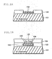
- an oxide film is formed on a silicon wafer (hereafter referred to as Si substrate) 101 of 600 ⁇ m in thickness, a metal (A1, A1 alloy or copper, for example) pad 102 is formed on the oxide film, and an SiO 2 film or a PSG film is formed by plasma CVD to cover the pad 102, forming a first oxide film 103 of a predetermined thickness together with the oxide film, as shown in Fig. 1A .
- the pad 102 is connected with a semiconductor element formed in the Si substrate 101.
- the first oxide film 103 may be ground physically or etched chemically, for example, when extra flatness is required.
- a portion (surface portion) of the pad 102 is exposed by etching the first oxide film 103 on the pad 102 using a photoresist film (not shown) as a mask.
- Total thickness of the first oxide film 103 is about 5 ⁇ m in this embodiment.
- a polyimide film is formed on the pad 102 and the first oxide film 103, and the polyimide film is etched using a photoresist film (not shown) as a mask to form a polyimide film 104 having an opening on the pad 102, as shown in Fig. 1B .
- nickel (Ni) 105 and gold (Au) 106 are formed in the opening, copper (Cu) is plated on them to fill the opening with a Cu post 107.
- Au can be plated on the Cu post 107 in order to protect the Cu post 107 from corrosion.
- Total thickness of the conductive materials (Ni, Au, Cu and Au) filled in the opening is about 25 ⁇ m in this embodiment.
- a holding substrate 111 may be bonded on the Si substrate 1 without the polyimide film 104 using a bonding film.
- titan-tungsten (TiW) 121 is formed on the pad 102 and the first oxide film 103, and is shaped into a predetermined pattern. Then a polyimide film 104A is formed and a Cu post 107A (and Au) is formed in an opening formed in the polyimide film 104A, adopting so-called re-distribution structure. Au may be plated on the Cu post 107A.
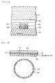
- a bonding film 110 is applied on the polyimide film 104 and the Cu post 107 (or on Au on the Cu post 107), and a holding substrate 111 and the Si substrate 101 are bonded together through the bonding film 110, as shown in Fig. 11A.
- the holding substrate 111 is a holding material to prevent the Si substrate 101 from cracking during back-grinding of the Si substrate 101. Thickness of the holding substrate 8 is about 400 ⁇ m in this embodiment, as required as the holding material.
- An organic film soluble in acetone is adopted as the bonding film 110 in order to improve workability in separation process of the Si substrate 101 and the holding substrate 111. Thickness of the bonding film 110 is about 100 ⁇ m in this embodiment.
- An epoxy resin 112 will be placed on the wafer to surround the bonding film 110. The width of the epoxy resin 112 is about 2 mm from outer the edge of the wafer.
- a film without adhesiveness can be used in place of the bonding film, applying adhesive material on both sides of the film to bond the holding substrate 111 and the Si substrate 101 together.
- a solvent in which the adhesive material dissolves is used.
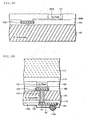
- Fig. 2B shows a cross-sectional view and a plan view of an outline of the semiconductor device shown in Fig. 2A (the holding substrate 111 is omitted for convenience of explanation).
- the bonding film 110 is sealed and fixed by packing the periphery of the bonding film 110 with the epoxy resin 112, as shown in Fig. 2B . Infiltration of chemical solution such as an organic solvent during various kinds of processing is prevented.
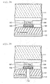
- the Si substrate 101 is back-ground to make the Si substrate 101 about 10 to 100 ⁇ m thick, as shown in Fig. 3A .
- the holding substrate 111 bolsters the Si substrate 101 during the back-grinding process.
- a second oxide film 113 of 0.01 ⁇ m in thickness is formed on a back surface of the Si substrate 101 which is back-ground.
- a silicon nitride film or an organic insulating material made of polyimide can be used instead of the second oxide film 113. Workability in the back-grind process is good because flatness of surface including the Cu post 107 does not matter and no additional processing is required.
- An opening 114 is formed by etching the second oxide film 113 and the Si substrate 101 using a photoresist film (not shown) as a mask, as shown in Fig. 3B .
- the first oxide film 103 exposed in the opening 114 is etched to expose the pad 102, as shown in Fig. 4A .
- a third oxide film is formed by CVD method to cover the second oxide film 113 and the pad 102 in the opening 114a, and the third oxide film is anisotropically etched to remain on the sidewall of the opening 114a, forming a sidewall spacer film 115.
- the CVD processing of the third oxide film is made, for example, at low temperature of about 200°C.
- the sidewall spacer 115 may be made of silicon nitride film.
- a barrier film 116 made of titanium nitride (TiN) or tantalum nitride (TaN) is sputtered in the opening 114a through the sidewall spacer 115, and copper is filled in the opening 114a through the barrier film 116 to form a Cu buried layer 117, as shown in Fig. 4B .
- This process step includes Cu seeding, Cu plating and Cu annealing. Then, copper is buried in the opening 114a. When extra flatness is required, the copper is polished by CMP.
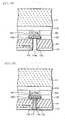
- solder mask 118 with an opening somewhat wider than the opening 114a filled with Cu is formed on the Cu buried layer 117, and a solder paste is screen-printed in the opening through the solder mask 118 followed by reflow processing of the solder paste to form a solder ball 119 on the Cu buried layer 117, as shown in Fig. 5A .
- a polyimide film made of Rika-coat (a product of New Japan Chemical Co., Ltd.), which can be imidized at 200°C is used as the solder mask 118 in this embodiment.
- an aluminum film 131 and a nickel film (and a gold film) 132 are formed on the Cu buried layer 117 and the second oxide film 113, and are shaped into a predetermined pattern.
- a structure in which a solder ball 119A is formed through a solder mask 118A can be adopted.
- the device is diced from the side of the Si substrate to the depth reaching the bonding film 110.
- Acetone infiltrates through dicing lines D shown in Fig. 6B to dissolve the bonding film 110, when the Si substrate 101 is immersed in acetone in a solvent tank (not shown).
- the Si substrate 101 each die and the holding substrate 111 are separated to complete each CSP die 120 as shown in Fig. 6A .
- the Si substrate 101 and the holding substrate 111 are separated simply by immersing them in acetone after dicing, providing good workability, since the organic bonding film 110 which is soluble in acetone is used to bond the Si substrate 101 and the holding substrate 8 together in this embodiment.
- a film having weak adhesion may be used instead of the bonding film 110, and the dice can be peeled off physically after dicing.
- a transparent glass is used as the holding substrate 111, a UV-tape is applied as the organic bonding film 110 and the dice are separated by exposing them to ultraviolet radiation after dicing.
- the Si substrate 101 and the holding substrate 111 are bonded with a non-adhesive film to which UV-type adhesive material is applied in place of the bonding film 110, the Si substrate 101 may be diced after separating the Si substrate 101 and the holding substrate 111 by exposing the UV-type adhesive material to ultraviolet radiation in a later process step and hardening it.
- the wafer and the holding substrate 111 may be separated by heating the back side of the wafer with a hot plate to melt and soften the organic film (bonding film) 110 sandwiched between the wafer and the holding substrate 111.
- the bonding film 110 is the organic film soluble in acetone, it would melt when heated to about 200°C, and if the bonding film 110 is the polyimide film, it would melt when heated to about 400°C.
- wirings are formed with apparatuses such as a sputtering apparatus and a plating apparatus which are used commonly in assembly.
- apparatuses such as a sputtering apparatus and a plating apparatus which are used commonly in assembly.
- the semiconductor devices are manufactured with a very simple manufacturing process at low cost.
- re-distribution wiring to connect a Cu via and a pad after forming the Cu via is not needed, eliminating any additional process step.
- thickness of the chip may be reduced as much as possible, since the holding substrate and the Si substrate are subject to back-grinding and the subsequent processing after they are bonded together.
Landscapes
- Internal Circuitry In Semiconductor Integrated Circuit Devices (AREA)
- Mechanical Treatment Of Semiconductor (AREA)
- Pressure Sensors (AREA)
Applications Claiming Priority (2)
| Application Number | Priority Date | Filing Date | Title |
|---|---|---|---|
| JP2002176775 | 2002-06-18 | ||
| EP03013839A EP1376678A3 (de) | 2002-06-18 | 2003-06-18 | Herstellungsverfahren für Halbleiterbauelement |
Related Parent Applications (1)
| Application Number | Title | Priority Date | Filing Date |
|---|---|---|---|
| EP03013839.0 Division | 2003-06-18 |
Publications (2)
| Publication Number | Publication Date |
|---|---|
| EP2207198A2 true EP2207198A2 (de) | 2010-07-14 |
| EP2207198A3 EP2207198A3 (de) | 2011-06-29 |
Family
ID=29717459
Family Applications (2)
| Application Number | Title | Priority Date | Filing Date |
|---|---|---|---|
| EP03013839A Withdrawn EP1376678A3 (de) | 2002-06-18 | 2003-06-18 | Herstellungsverfahren für Halbleiterbauelement |
| EP10003219A Withdrawn EP2207198A3 (de) | 2002-06-18 | 2003-06-18 | Herstellungsverfahren für ein Halbleiterbauelement |
Family Applications Before (1)
| Application Number | Title | Priority Date | Filing Date |
|---|---|---|---|
| EP03013839A Withdrawn EP1376678A3 (de) | 2002-06-18 | 2003-06-18 | Herstellungsverfahren für Halbleiterbauelement |
Country Status (5)
| Country | Link |
|---|---|
| US (2) | US6864172B2 (de) |
| EP (2) | EP1376678A3 (de) |
| KR (1) | KR100552356B1 (de) |
| CN (2) | CN1276492C (de) |
| TW (1) | TWI229435B (de) |
Families Citing this family (153)
| Publication number | Priority date | Publication date | Assignee | Title |
|---|---|---|---|---|
| TWI232560B (en) * | 2002-04-23 | 2005-05-11 | Sanyo Electric Co | Semiconductor device and its manufacture |
| US7399683B2 (en) * | 2002-06-18 | 2008-07-15 | Sanyo Electric Co., Ltd. | Manufacturing method of semiconductor device |
| TWI229435B (en) | 2002-06-18 | 2005-03-11 | Sanyo Electric Co | Manufacture of semiconductor device |
| JP2004095849A (ja) * | 2002-08-30 | 2004-03-25 | Fujikura Ltd | 貫通電極付き半導体基板の製造方法、貫通電極付き半導体デバイスの製造方法 |
| TWI227550B (en) * | 2002-10-30 | 2005-02-01 | Sanyo Electric Co | Semiconductor device manufacturing method |
| JP4071615B2 (ja) * | 2002-12-20 | 2008-04-02 | 株式会社フジクラ | 貫通電極の形成方法及び貫通電極付き基板 |
| JP4401181B2 (ja) | 2003-08-06 | 2010-01-20 | 三洋電機株式会社 | 半導体装置及びその製造方法 |
| US7180149B2 (en) * | 2003-08-28 | 2007-02-20 | Fujikura Ltd. | Semiconductor package with through-hole |
| DE10340409B4 (de) * | 2003-09-02 | 2007-05-24 | Fraunhofer-Gesellschaft zur Förderung der angewandten Forschung e.V. | Trägerwafer und Verfahren zum Bearbeiten eines Halbleiterwafers unter Verwendung eines Trägerwafers |
| EP1515364B1 (de) | 2003-09-15 | 2016-04-13 | Nuvotronics, LLC | Gehäuse und Verfahren zu seiner Herstellung und zu seiner Prüfung |
| US6934065B2 (en) * | 2003-09-18 | 2005-08-23 | Micron Technology, Inc. | Microelectronic devices and methods for packaging microelectronic devices |
| TWI226090B (en) * | 2003-09-26 | 2005-01-01 | Advanced Semiconductor Eng | Transparent packaging in wafer level |
| KR100529672B1 (ko) * | 2003-10-02 | 2005-11-17 | 동부아남반도체 주식회사 | 이미지 센서의 백 그라인딩 방법 |
| US7081411B2 (en) * | 2003-10-18 | 2006-07-25 | Northrop Grumman Corporation | Wafer etching techniques |
| US7091124B2 (en) | 2003-11-13 | 2006-08-15 | Micron Technology, Inc. | Methods for forming vias in microelectronic devices, and methods for packaging microelectronic devices |
| US8084866B2 (en) | 2003-12-10 | 2011-12-27 | Micron Technology, Inc. | Microelectronic devices and methods for filling vias in microelectronic devices |
| US7583862B2 (en) * | 2003-11-26 | 2009-09-01 | Aptina Imaging Corporation | Packaged microelectronic imagers and methods of packaging microelectronic imagers |
| US20050147489A1 (en) * | 2003-12-24 | 2005-07-07 | Tian-An Chen | Wafer supporting system for semiconductor wafers |
| TWI249767B (en) * | 2004-02-17 | 2006-02-21 | Sanyo Electric Co | Method for making a semiconductor device |
| JP4850392B2 (ja) | 2004-02-17 | 2012-01-11 | 三洋電機株式会社 | 半導体装置の製造方法 |
| JP4307284B2 (ja) | 2004-02-17 | 2009-08-05 | 三洋電機株式会社 | 半導体装置の製造方法 |
| JP2005235860A (ja) | 2004-02-17 | 2005-09-02 | Sanyo Electric Co Ltd | 半導体装置及びその製造方法 |
| US7253397B2 (en) | 2004-02-23 | 2007-08-07 | Micron Technology, Inc. | Packaged microelectronic imagers and methods of packaging microelectronic imagers |
| JP2005303258A (ja) * | 2004-03-16 | 2005-10-27 | Fujikura Ltd | デバイス及びその製造方法 |
| US20050247894A1 (en) | 2004-05-05 | 2005-11-10 | Watkins Charles M | Systems and methods for forming apertures in microfeature workpieces |
| US8092734B2 (en) * | 2004-05-13 | 2012-01-10 | Aptina Imaging Corporation | Covers for microelectronic imagers and methods for wafer-level packaging of microelectronics imagers |
| US7253957B2 (en) * | 2004-05-13 | 2007-08-07 | Micron Technology, Inc. | Integrated optics units and methods of manufacturing integrated optics units for use with microelectronic imagers |
| US20050275750A1 (en) * | 2004-06-09 | 2005-12-15 | Salman Akram | Wafer-level packaged microelectronic imagers and processes for wafer-level packaging |
| US7498647B2 (en) | 2004-06-10 | 2009-03-03 | Micron Technology, Inc. | Packaged microelectronic imagers and methods of packaging microelectronic imagers |
| US7262405B2 (en) * | 2004-06-14 | 2007-08-28 | Micron Technology, Inc. | Prefabricated housings for microelectronic imagers |
| US7199439B2 (en) * | 2004-06-14 | 2007-04-03 | Micron Technology, Inc. | Microelectronic imagers and methods of packaging microelectronic imagers |
| KR100618543B1 (ko) * | 2004-06-15 | 2006-08-31 | 삼성전자주식회사 | 웨이퍼 레벨 적층 패키지용 칩 스케일 패키지 제조 방법 |
| US7232754B2 (en) * | 2004-06-29 | 2007-06-19 | Micron Technology, Inc. | Microelectronic devices and methods for forming interconnects in microelectronic devices |
| US7294897B2 (en) * | 2004-06-29 | 2007-11-13 | Micron Technology, Inc. | Packaged microelectronic imagers and methods of packaging microelectronic imagers |
| JP4376715B2 (ja) * | 2004-07-16 | 2009-12-02 | 三洋電機株式会社 | 半導体装置の製造方法 |
| US7416913B2 (en) * | 2004-07-16 | 2008-08-26 | Micron Technology, Inc. | Methods of manufacturing microelectronic imaging units with discrete standoffs |
| US7189954B2 (en) * | 2004-07-19 | 2007-03-13 | Micron Technology, Inc. | Microelectronic imagers with optical devices and methods of manufacturing such microelectronic imagers |
| US7402453B2 (en) * | 2004-07-28 | 2008-07-22 | Micron Technology, Inc. | Microelectronic imaging units and methods of manufacturing microelectronic imaging units |
| JP4322181B2 (ja) * | 2004-07-29 | 2009-08-26 | 三洋電機株式会社 | 半導体装置の製造方法 |
| US20060023107A1 (en) * | 2004-08-02 | 2006-02-02 | Bolken Todd O | Microelectronic imagers with optics supports having threadless interfaces and methods for manufacturing such microelectronic imagers |
| US7364934B2 (en) * | 2004-08-10 | 2008-04-29 | Micron Technology, Inc. | Microelectronic imaging units and methods of manufacturing microelectronic imaging units |
| US7397066B2 (en) * | 2004-08-19 | 2008-07-08 | Micron Technology, Inc. | Microelectronic imagers with curved image sensors and methods for manufacturing microelectronic imagers |
| US7223626B2 (en) * | 2004-08-19 | 2007-05-29 | Micron Technology, Inc. | Spacers for packaged microelectronic imagers and methods of making and using spacers for wafer-level packaging of imagers |
| WO2006018787A2 (en) * | 2004-08-20 | 2006-02-23 | Philips Intellectual Property & Standards Gmbh | Method of detaching a thin semiconductor circuit from its base |
| US7115961B2 (en) * | 2004-08-24 | 2006-10-03 | Micron Technology, Inc. | Packaged microelectronic imaging devices and methods of packaging microelectronic imaging devices |
| US7429494B2 (en) * | 2004-08-24 | 2008-09-30 | Micron Technology, Inc. | Microelectronic imagers with optical devices having integral reference features and methods for manufacturing such microelectronic imagers |
| US7425499B2 (en) * | 2004-08-24 | 2008-09-16 | Micron Technology, Inc. | Methods for forming interconnects in vias and microelectronic workpieces including such interconnects |
| US7276393B2 (en) * | 2004-08-26 | 2007-10-02 | Micron Technology, Inc. | Microelectronic imaging units and methods of manufacturing microelectronic imaging units |
| SG120200A1 (en) * | 2004-08-27 | 2006-03-28 | Micron Technology Inc | Slanted vias for electrical circuits on circuit boards and other substrates |
| US7419852B2 (en) | 2004-08-27 | 2008-09-02 | Micron Technology, Inc. | Low temperature methods of forming back side redistribution layers in association with through wafer interconnects, semiconductor devices including same, and assemblies |
| US20070148807A1 (en) | 2005-08-22 | 2007-06-28 | Salman Akram | Microelectronic imagers with integrated optical devices and methods for manufacturing such microelectronic imagers |
| US7511262B2 (en) * | 2004-08-30 | 2009-03-31 | Micron Technology, Inc. | Optical device and assembly for use with imaging dies, and wafer-label imager assembly |
| US7491582B2 (en) * | 2004-08-31 | 2009-02-17 | Seiko Epson Corporation | Method for manufacturing semiconductor device and semiconductor device |
| US7646075B2 (en) * | 2004-08-31 | 2010-01-12 | Micron Technology, Inc. | Microelectronic imagers having front side contacts |
| JP2006071486A (ja) * | 2004-09-02 | 2006-03-16 | Renesas Technology Corp | 接続装置、半導体チップ検査装置および半導体装置の製造方法 |
| US7300857B2 (en) * | 2004-09-02 | 2007-11-27 | Micron Technology, Inc. | Through-wafer interconnects for photoimager and memory wafers |
| JP4966487B2 (ja) * | 2004-09-29 | 2012-07-04 | オンセミコンダクター・トレーディング・リミテッド | 半導体装置及びその製造方法 |
| TWI267183B (en) | 2004-09-29 | 2006-11-21 | Sanyo Electric Co | Semiconductor device and manufacturing method of the same |
| JP4246132B2 (ja) * | 2004-10-04 | 2009-04-02 | シャープ株式会社 | 半導体装置およびその製造方法 |
| JP4443379B2 (ja) | 2004-10-26 | 2010-03-31 | 三洋電機株式会社 | 半導体装置の製造方法 |
| TWI303864B (en) | 2004-10-26 | 2008-12-01 | Sanyo Electric Co | Semiconductor device and method for making the same |
| JP4873517B2 (ja) * | 2004-10-28 | 2012-02-08 | オンセミコンダクター・トレーディング・リミテッド | 半導体装置及びその製造方法 |
| US7271482B2 (en) * | 2004-12-30 | 2007-09-18 | Micron Technology, Inc. | Methods for forming interconnects in microelectronic workpieces and microelectronic workpieces formed using such methods |
| US20060162850A1 (en) * | 2005-01-24 | 2006-07-27 | Micron Technology, Inc. | Methods and apparatus for releasably attaching microfeature workpieces to support members |
| US7214919B2 (en) * | 2005-02-08 | 2007-05-08 | Micron Technology, Inc. | Microelectronic imaging units and methods of manufacturing microelectronic imaging units |
| US20060177999A1 (en) * | 2005-02-10 | 2006-08-10 | Micron Technology, Inc. | Microelectronic workpieces and methods for forming interconnects in microelectronic workpieces |
| US7303931B2 (en) * | 2005-02-10 | 2007-12-04 | Micron Technology, Inc. | Microfeature workpieces having microlenses and methods of forming microlenses on microfeature workpieces |
| US7190039B2 (en) * | 2005-02-18 | 2007-03-13 | Micron Technology, Inc. | Microelectronic imagers with shaped image sensors and methods for manufacturing microelectronic imagers |
| US7485967B2 (en) | 2005-03-10 | 2009-02-03 | Sanyo Electric Co., Ltd. | Semiconductor device with via hole for electric connection |
| JP4097660B2 (ja) * | 2005-04-06 | 2008-06-11 | シャープ株式会社 | 半導体装置 |
| DE102005022017B3 (de) * | 2005-05-12 | 2006-10-26 | Infineon Technologies Ag | Verfahren zur Herstellung von Chip-Stapeln sowie zugehörige Chip-Stapel |
| JP4311376B2 (ja) | 2005-06-08 | 2009-08-12 | セイコーエプソン株式会社 | 半導体装置、半導体装置の製造方法、電子部品、回路基板及び電子機器 |
| US7795134B2 (en) | 2005-06-28 | 2010-09-14 | Micron Technology, Inc. | Conductive interconnect structures and formation methods using supercritical fluids |
| US20060290001A1 (en) * | 2005-06-28 | 2006-12-28 | Micron Technology, Inc. | Interconnect vias and associated methods of formation |
| US7169248B1 (en) * | 2005-07-19 | 2007-01-30 | Micron Technology, Inc. | Methods for releasably attaching support members to microfeature workpieces and microfeature assemblies formed using such methods |
| US7485968B2 (en) * | 2005-08-11 | 2009-02-03 | Ziptronix, Inc. | 3D IC method and device |
| US7262134B2 (en) * | 2005-09-01 | 2007-08-28 | Micron Technology, Inc. | Microfeature workpieces and methods for forming interconnects in microfeature workpieces |
| US7863187B2 (en) * | 2005-09-01 | 2011-01-04 | Micron Technology, Inc. | Microfeature workpieces and methods for forming interconnects in microfeature workpieces |
| US7772116B2 (en) | 2005-09-01 | 2010-08-10 | Micron Technology, Inc. | Methods of forming blind wafer interconnects |
| US7622377B2 (en) | 2005-09-01 | 2009-11-24 | Micron Technology, Inc. | Microfeature workpiece substrates having through-substrate vias, and associated methods of formation |
| US7288757B2 (en) * | 2005-09-01 | 2007-10-30 | Micron Technology, Inc. | Microelectronic imaging devices and associated methods for attaching transmissive elements |
| JP4745007B2 (ja) * | 2005-09-29 | 2011-08-10 | 三洋電機株式会社 | 半導体装置及びその製造方法 |
| US20080217715A1 (en) * | 2005-10-11 | 2008-09-11 | Park Tae-Seok | Wafer Level Package Using Silicon Via Contacts for Cmos Image Sensor and Method of Fabricating the Same |
| DE102005053494A1 (de) * | 2005-11-09 | 2007-05-16 | Fraunhofer Ges Forschung | Verfahren zum Herstellen elektrisch leitender Durchführungen durch nicht- oder halbleitende Substrate |
| TWI324800B (en) * | 2005-12-28 | 2010-05-11 | Sanyo Electric Co | Method for manufacturing semiconductor device |
| TW200737506A (en) * | 2006-03-07 | 2007-10-01 | Sanyo Electric Co | Semiconductor device and manufacturing method of the same |
| US7749349B2 (en) * | 2006-03-14 | 2010-07-06 | Micron Technology, Inc. | Methods and systems for releasably attaching support members to microfeature workpieces |
| JP4812512B2 (ja) | 2006-05-19 | 2011-11-09 | オンセミコンダクター・トレーディング・リミテッド | 半導体装置の製造方法 |
| US7749899B2 (en) | 2006-06-01 | 2010-07-06 | Micron Technology, Inc. | Microelectronic workpieces and methods and systems for forming interconnects in microelectronic workpieces |
| TWI367557B (en) * | 2006-08-11 | 2012-07-01 | Sanyo Electric Co | Semiconductor device and manufaturing method thereof |
| US7629249B2 (en) | 2006-08-28 | 2009-12-08 | Micron Technology, Inc. | Microfeature workpieces having conductive interconnect structures formed by chemically reactive processes, and associated systems and methods |
| US7902643B2 (en) | 2006-08-31 | 2011-03-08 | Micron Technology, Inc. | Microfeature workpieces having interconnects and conductive backplanes, and associated systems and methods |
| US7829438B2 (en) | 2006-10-10 | 2010-11-09 | Tessera, Inc. | Edge connect wafer level stacking |
| US8513789B2 (en) | 2006-10-10 | 2013-08-20 | Tessera, Inc. | Edge connect wafer level stacking with leads extending along edges |
| US7901989B2 (en) | 2006-10-10 | 2011-03-08 | Tessera, Inc. | Reconstituted wafer level stacking |
| JP5010247B2 (ja) * | 2006-11-20 | 2012-08-29 | オンセミコンダクター・トレーディング・リミテッド | 半導体装置及びその製造方法 |
| US8569876B2 (en) | 2006-11-22 | 2013-10-29 | Tessera, Inc. | Packaged semiconductor chips with array |
| US7791199B2 (en) * | 2006-11-22 | 2010-09-07 | Tessera, Inc. | Packaged semiconductor chips |
| US7952195B2 (en) | 2006-12-28 | 2011-05-31 | Tessera, Inc. | Stacked packages with bridging traces |
| US7679187B2 (en) * | 2007-01-11 | 2010-03-16 | Visera Technologies Company Limited | Bonding pad structure for back illuminated optoelectronic device and fabricating method thereof |
| JP4919984B2 (ja) * | 2007-02-25 | 2012-04-18 | サムスン エレクトロニクス カンパニー リミテッド | 電子デバイスパッケージとその形成方法 |
| EP2135280A2 (de) * | 2007-03-05 | 2009-12-23 | Tessera, Inc. | Chips mit rückseitigen kontakten, die durch durchkontaktierungen mit vorderseitigen kontakten verbunden werden |
| US8232183B2 (en) * | 2007-05-04 | 2012-07-31 | Taiwan Semiconductor Manufacturing Company, Ltd. | Process and apparatus for wafer-level flip-chip assembly |
| JP5101157B2 (ja) * | 2007-05-07 | 2012-12-19 | オンセミコンダクター・トレーディング・リミテッド | 半導体装置の製造方法 |
| JP2009021462A (ja) * | 2007-07-13 | 2009-01-29 | Disco Abrasive Syst Ltd | ウェーハの加工方法 |
| CN101809739B (zh) | 2007-07-27 | 2014-08-20 | 泰塞拉公司 | 具有后应用的衬垫延长部分的重构晶片堆封装 |
| KR101538648B1 (ko) * | 2007-07-31 | 2015-07-22 | 인벤사스 코포레이션 | 실리콘 쓰루 비아를 사용하는 반도체 패키지 공정 |
| WO2009020572A2 (en) | 2007-08-03 | 2009-02-12 | Tessera Technologies Hungary Kft. | Stack packages using reconstituted wafers |
| US8043895B2 (en) | 2007-08-09 | 2011-10-25 | Tessera, Inc. | Method of fabricating stacked assembly including plurality of stacked microelectronic elements |
| SG150410A1 (en) | 2007-08-31 | 2009-03-30 | Micron Technology Inc | Partitioned through-layer via and associated systems and methods |
| US7884015B2 (en) | 2007-12-06 | 2011-02-08 | Micron Technology, Inc. | Methods for forming interconnects in microelectronic workpieces and microelectronic workpieces formed using such methods |
| JP5271562B2 (ja) * | 2008-02-15 | 2013-08-21 | 本田技研工業株式会社 | 半導体装置および半導体装置の製造方法 |
| US20100053407A1 (en) * | 2008-02-26 | 2010-03-04 | Tessera, Inc. | Wafer level compliant packages for rear-face illuminated solid state image sensors |
| US20090212381A1 (en) * | 2008-02-26 | 2009-08-27 | Tessera, Inc. | Wafer level packages for rear-face illuminated solid state image sensors |
| JP5639052B2 (ja) | 2008-06-16 | 2014-12-10 | テッセラ,インコーポレイテッド | ウェハレベルでの縁部の積重ね |
| DE102009005458B4 (de) * | 2009-01-21 | 2010-09-30 | Austriamicrosystems Ag | Halbleiterbauelement mit Durchkontaktierung und Verfahren zu dessen Herstellung |
| US20100194465A1 (en) * | 2009-02-02 | 2010-08-05 | Ali Salih | Temperature compensated current source and method therefor |
| US8466542B2 (en) | 2009-03-13 | 2013-06-18 | Tessera, Inc. | Stacked microelectronic assemblies having vias extending through bond pads |
| EP2306506B1 (de) | 2009-10-01 | 2013-07-31 | ams AG | Verfahren zur Herstellung einer Halbleitervorrichtung mit einer Durchkontaktierung |
| TWI497658B (zh) * | 2009-10-07 | 2015-08-21 | 精材科技股份有限公司 | 晶片封裝體及其製造方法 |
| US8796135B2 (en) | 2010-07-23 | 2014-08-05 | Tessera, Inc. | Microelectronic elements with rear contacts connected with via first or via middle structures |
| US9640437B2 (en) | 2010-07-23 | 2017-05-02 | Tessera, Inc. | Methods of forming semiconductor elements using micro-abrasive particle stream |
| US8791575B2 (en) | 2010-07-23 | 2014-07-29 | Tessera, Inc. | Microelectronic elements having metallic pads overlying vias |
| JP2012039005A (ja) * | 2010-08-10 | 2012-02-23 | Toshiba Corp | 半導体装置およびその製造方法 |
| US8847380B2 (en) | 2010-09-17 | 2014-09-30 | Tessera, Inc. | Staged via formation from both sides of chip |
| US8610259B2 (en) | 2010-09-17 | 2013-12-17 | Tessera, Inc. | Multi-function and shielded 3D interconnects |
| US8455984B2 (en) * | 2010-11-15 | 2013-06-04 | Nanya Technology Corp. | Integrated circuit structure and method of forming the same |
| KR101059490B1 (ko) | 2010-11-15 | 2011-08-25 | 테세라 리써치 엘엘씨 | 임베드된 트레이스에 의해 구성된 전도성 패드 |
| US8736066B2 (en) | 2010-12-02 | 2014-05-27 | Tessera, Inc. | Stacked microelectronic assemby with TSVS formed in stages and carrier above chip |
| US8637968B2 (en) | 2010-12-02 | 2014-01-28 | Tessera, Inc. | Stacked microelectronic assembly having interposer connecting active chips |
| US8587126B2 (en) | 2010-12-02 | 2013-11-19 | Tessera, Inc. | Stacked microelectronic assembly with TSVs formed in stages with plural active chips |
| US8610264B2 (en) | 2010-12-08 | 2013-12-17 | Tessera, Inc. | Compliant interconnects in wafers |
| KR20120077876A (ko) * | 2010-12-31 | 2012-07-10 | 삼성전자주식회사 | 이종 기판 접합 구조 및 방법 |
| KR20120135626A (ko) * | 2011-06-07 | 2012-12-17 | 삼성전자주식회사 | 반도체 칩 패키지의 제조 방법 |
| DE102011112659B4 (de) * | 2011-09-06 | 2022-01-27 | Vishay Semiconductor Gmbh | Oberflächenmontierbares elektronisches Bauelement |
| US8803326B2 (en) * | 2011-11-15 | 2014-08-12 | Xintec Inc. | Chip package |
| KR101906860B1 (ko) * | 2011-11-24 | 2018-10-12 | 삼성전자주식회사 | 반도체 소자 및 이를 제조하는 방법 |
| CN102795593A (zh) * | 2012-08-29 | 2012-11-28 | 深迪半导体(上海)有限公司 | 超薄真空密封mems晶圆的加工方法 |
| CN104112673B (zh) * | 2013-04-19 | 2017-06-23 | 碁鼎科技秦皇岛有限公司 | 芯片封装基板及其制作方法 |
| TWI525673B (zh) * | 2013-10-08 | 2016-03-11 | 精材科技股份有限公司 | 晶圓級晶片封裝體的製造方法 |
| KR20150078008A (ko) * | 2013-12-30 | 2015-07-08 | 에스케이하이닉스 주식회사 | 반도체 장치, 이의 제조 방법 및 이의 테스트 방법 |
| CN104752239B (zh) * | 2013-12-31 | 2019-07-23 | 中芯国际集成电路制造(上海)有限公司 | 一种半导体器件、制备方法及封装方法 |
| DE102014100237B4 (de) * | 2014-01-10 | 2016-06-02 | Stiftung Caesar Center Of Advanced European Studies And Research | Verfahren zum Erzeugen einer freistehenden, abgeschirmten Metallelektrode durch einen Einzelmaskenprozess und ein Verfahren zum Freilegen einer Elektrodenspitze |
| TWI628723B (zh) * | 2015-03-10 | 2018-07-01 | 精材科技股份有限公司 | 一種晶片尺寸等級的感測晶片封裝體及其製造方法 |
| TWI778938B (zh) | 2015-03-16 | 2022-10-01 | 美商艾馬克科技公司 | 半導體裝置和製造其之方法 |
| KR101678418B1 (ko) * | 2015-03-16 | 2016-11-23 | 한국생산기술연구원 | 3차원 레이저 스캐닝 시스템 |
| US9953941B2 (en) | 2015-08-25 | 2018-04-24 | Invensas Bonding Technologies, Inc. | Conductive barrier direct hybrid bonding |
| US20170256432A1 (en) * | 2016-03-03 | 2017-09-07 | Nexperia B.V. | Overmolded chip scale package |
| US20170330980A1 (en) * | 2016-05-16 | 2017-11-16 | General Electric Company | Die repatterning transmission lines on silicon photomultipliers |
| US10319654B1 (en) | 2017-12-01 | 2019-06-11 | Cubic Corporation | Integrated chip scale packages |
| US11114402B2 (en) | 2018-02-23 | 2021-09-07 | Semiconductor Components Industries, Llc | Semiconductor device with backmetal and related methods |
| CN110444480A (zh) * | 2019-07-24 | 2019-11-12 | 浙江荷清柔性电子技术有限公司 | 制作柔性芯片的方法、柔性芯片 |
| CN119108478B (zh) * | 2023-06-01 | 2026-01-09 | 重庆康佳光电科技有限公司 | 发光芯片制备方法 |
Family Cites Families (116)
| Publication number | Priority date | Publication date | Assignee | Title |
|---|---|---|---|---|
| DE1933731C3 (de) | 1968-07-05 | 1982-03-25 | Honeywell Information Systems Italia S.p.A., Caluso, Torino | Verfahren zum Herstellen einer integrierten Halbleiterschaltung |
| GB1285708A (en) | 1968-10-28 | 1972-08-16 | Lucas Industries Ltd | Semi-conductor devices |
| US3648131A (en) | 1969-11-07 | 1972-03-07 | Ibm | Hourglass-shaped conductive connection through semiconductor structures |
| US4954875A (en) | 1986-07-17 | 1990-09-04 | Laser Dynamics, Inc. | Semiconductor wafer array with electrically conductive compliant material |
| US4978639A (en) | 1989-01-10 | 1990-12-18 | Avantek, Inc. | Method for the simultaneous formation of via-holes and wraparound plating on semiconductor chips |
| JPH0482215A (ja) | 1990-07-25 | 1992-03-16 | Sumitomo Electric Ind Ltd | ランプアニール装置 |
| US5229647A (en) | 1991-03-27 | 1993-07-20 | Micron Technology, Inc. | High density data storage using stacked wafers |
| US5927993A (en) | 1992-02-03 | 1999-07-27 | Motorola, Inc. | Backside processing method |
| US5350662A (en) * | 1992-03-26 | 1994-09-27 | Hughes Aircraft Company | Maskless process for forming refractory metal layer in via holes of GaAs chips |
| US5476819A (en) | 1993-07-26 | 1995-12-19 | Litton Systems, Inc. | Substrate anchor for undercut silicon on insulator microstructures |
| TW270213B (de) | 1993-12-08 | 1996-02-11 | Matsushita Electric Industrial Co Ltd | |
| JPH08186151A (ja) | 1994-12-29 | 1996-07-16 | Sony Corp | 半導体装置及びその製造方法 |
| US5682062A (en) | 1995-06-05 | 1997-10-28 | Harris Corporation | System for interconnecting stacked integrated circuits |
| US5648684A (en) | 1995-07-26 | 1997-07-15 | International Business Machines Corporation | Endcap chip with conductive, monolithic L-connect for multichip stack |
| JPH0946566A (ja) | 1995-08-01 | 1997-02-14 | Olympus Optical Co Ltd | 電子内視鏡用固体撮像装置 |
| US5904546A (en) | 1996-02-12 | 1999-05-18 | Micron Technology, Inc. | Method and apparatus for dicing semiconductor wafers |
| KR100410812B1 (ko) | 1996-06-25 | 2004-04-01 | 주식회사 하이닉스반도체 | 반도체장치의제조방법 |
| US6027958A (en) * | 1996-07-11 | 2000-02-22 | Kopin Corporation | Transferred flexible integrated circuit |
| DE19636744C2 (de) | 1996-09-10 | 1998-09-17 | Siemens Ag | Verfahren zum Übertragen von Daten in einem hybriden Telekommunikationssystem, insbesondere einem "ISDN - DECT-spezifischen RLL/WLL"-System |
| WO1998013862A1 (fr) | 1996-09-24 | 1998-04-02 | Mitsubishi Denki Kabushiki Kaisha | Dispositif a semi-conducteur et son procede de fabrication |
| US5691245A (en) * | 1996-10-28 | 1997-11-25 | He Holdings, Inc. | Methods of forming two-sided HDMI interconnect structures |
| JP3537447B2 (ja) | 1996-10-29 | 2004-06-14 | トル‐シ・テクノロジーズ・インコーポレイテッド | 集積回路及びその製造方法 |
| US6054760A (en) | 1996-12-23 | 2000-04-25 | Scb Technologies Inc. | Surface-connectable semiconductor bridge elements and devices including the same |
| US5910687A (en) | 1997-01-24 | 1999-06-08 | Chipscale, Inc. | Wafer fabrication of die-bottom contacts for electronic devices |
| JPH10242084A (ja) | 1997-02-24 | 1998-09-11 | Lintec Corp | ウェハ貼着用粘着シートおよび電子部品の製造方法 |
| JP3286553B2 (ja) | 1997-03-17 | 2002-05-27 | 株式会社村上開明堂 | 防眩インナーミラー |
| JP3011233B2 (ja) | 1997-05-02 | 2000-02-21 | 日本電気株式会社 | 半導体パッケージ及びその半導体実装構造 |
| US6051489A (en) | 1997-05-13 | 2000-04-18 | Chipscale, Inc. | Electronic component package with posts on the active side of the substrate |
| JP3335575B2 (ja) | 1997-06-06 | 2002-10-21 | 松下電器産業株式会社 | 半導体装置およびその製造方法 |
| FR2767223B1 (fr) | 1997-08-06 | 1999-09-17 | Commissariat Energie Atomique | Procede d'interconnexion a travers un materiau semi-conducteur, et dispositif obtenu |
| US6432744B1 (en) | 1997-11-20 | 2002-08-13 | Texas Instruments Incorporated | Wafer-scale assembly of chip-size packages |
| DE69737262T2 (de) | 1997-11-26 | 2007-11-08 | Stmicroelectronics S.R.L., Agrate Brianza | Herstellungsverfahren für einen Vorder-Hinterseiten-Durchkontakt in mikro-integrierten Schaltungen |
| US5888884A (en) | 1998-01-02 | 1999-03-30 | General Electric Company | Electronic device pad relocation, precision placement, and packaging in arrays |
| CN1288591A (zh) | 1998-01-20 | 2001-03-21 | 时至准钟表股份有限公司 | 半导体装置和制造方法及其安装构造和安装方法 |
| IL123207A0 (en) | 1998-02-06 | 1998-09-24 | Shellcase Ltd | Integrated circuit device |
| US6624505B2 (en) | 1998-02-06 | 2003-09-23 | Shellcase, Ltd. | Packaged integrated circuits and methods of producing thereof |
| JP3497722B2 (ja) | 1998-02-27 | 2004-02-16 | 富士通株式会社 | 半導体装置及びその製造方法及びその搬送トレイ |
| JP3842444B2 (ja) | 1998-07-24 | 2006-11-08 | 富士通株式会社 | 半導体装置の製造方法 |
| US6153929A (en) | 1998-08-21 | 2000-11-28 | Micron Technology, Inc. | Low profile multi-IC package connector |
| DE19846232A1 (de) | 1998-09-03 | 2000-03-09 | Fraunhofer Ges Forschung | Verfahren zur Herstellung eines Halbleiterbauelements mit Rückseitenkontaktierung |
| US6066513A (en) | 1998-10-02 | 2000-05-23 | International Business Machines Corporation | Process for precise multichip integration and product thereof |
| US6339251B2 (en) | 1998-11-10 | 2002-01-15 | Samsung Electronics Co., Ltd | Wafer grooves for reducing semiconductor wafer warping |
| US6310328B1 (en) | 1998-12-10 | 2001-10-30 | Mattson Technologies, Inc. | Rapid thermal processing chamber for processing multiple wafers |
| JP3687379B2 (ja) | 1998-12-18 | 2005-08-24 | 株式会社日立製作所 | 半導体装置の製造方法 |
| US6259039B1 (en) | 1998-12-29 | 2001-07-10 | Intel Corporation | Surface mount connector with pins in vias |
| KR100315030B1 (ko) | 1998-12-29 | 2002-04-24 | 박종섭 | 반도체패키지의제조방법 |
| FR2788375B1 (fr) | 1999-01-11 | 2003-07-18 | Gemplus Card Int | Procede de protection de puce de circuit integre |
| JP2000286283A (ja) | 1999-03-30 | 2000-10-13 | Seiko Epson Corp | 半導体装置の製造方法 |
| JP2000294677A (ja) * | 1999-04-05 | 2000-10-20 | Fujitsu Ltd | 高密度薄膜配線基板及びその製造方法 |
| US6617681B1 (en) * | 1999-06-28 | 2003-09-09 | Intel Corporation | Interposer and method of making same |
| US6326689B1 (en) | 1999-07-26 | 2001-12-04 | Stmicroelectronics, Inc. | Backside contact for touchchip |
| CN1322574C (zh) | 1999-07-30 | 2007-06-20 | 日本板硝子株式会社 | 在切割区中设置的槽的结构及其应用 |
| JP3687435B2 (ja) * | 1999-08-27 | 2005-08-24 | セイコーエプソン株式会社 | 半導体チップおよびその製造方法、半導体装置、コンピュータ、回路基板ならびに電子機器 |
| JP2001077229A (ja) | 1999-09-02 | 2001-03-23 | Matsushita Electronics Industry Corp | 半導体装置およびその製造方法 |
| US6316287B1 (en) | 1999-09-13 | 2001-11-13 | Vishay Intertechnology, Inc. | Chip scale surface mount packages for semiconductor device and process of fabricating the same |
| KR100462980B1 (ko) | 1999-09-13 | 2004-12-23 | 비쉐이 메저먼츠 그룹, 인코포레이티드 | 반도체장치용 칩 스케일 표면 장착 패키지 및 그 제조공정 |
| JP2001127243A (ja) | 1999-10-26 | 2001-05-11 | Sharp Corp | 積層半導体装置 |
| JP2001185519A (ja) | 1999-12-24 | 2001-07-06 | Hitachi Ltd | 半導体装置及びその製造方法 |
| JP3858545B2 (ja) | 1999-12-27 | 2006-12-13 | セイコーエプソン株式会社 | 半導体モジュール及び電子機器 |
| JP2001210667A (ja) | 2000-01-28 | 2001-08-03 | New Japan Radio Co Ltd | 半導体装置の製造方法 |
| US6534751B2 (en) | 2000-02-28 | 2003-03-18 | Kyocera Corporation | Wafer heating apparatus and ceramic heater, and method for producing the same |
| US6424031B1 (en) | 2000-05-08 | 2002-07-23 | Amkor Technology, Inc. | Stackable package with heat sink |
| JP3701542B2 (ja) | 2000-05-10 | 2005-09-28 | シャープ株式会社 | 半導体装置およびその製造方法 |
| JP3879816B2 (ja) | 2000-06-02 | 2007-02-14 | セイコーエプソン株式会社 | 半導体装置及びその製造方法、積層型半導体装置、回路基板並びに電子機器 |
| JP4329235B2 (ja) | 2000-06-27 | 2009-09-09 | セイコーエプソン株式会社 | 半導体装置及びその製造方法 |
| JP2002026270A (ja) | 2000-07-10 | 2002-01-25 | Nec Corp | 半導体装置の製造方法 |
| JP2002094082A (ja) | 2000-07-11 | 2002-03-29 | Seiko Epson Corp | 光素子及びその製造方法並びに電子機器 |
| JP2002057128A (ja) | 2000-08-15 | 2002-02-22 | Fujitsu Quantum Devices Ltd | 半導体装置及びその製造方法 |
| US6379982B1 (en) | 2000-08-17 | 2002-04-30 | Micron Technology, Inc. | Wafer on wafer packaging and method of fabrication for full-wafer burn-in and testing |
| US6406934B1 (en) | 2000-09-05 | 2002-06-18 | Amkor Technology, Inc. | Wafer level production of chip size semiconductor packages |
| JP2002083785A (ja) | 2000-09-07 | 2002-03-22 | Nec Kansai Ltd | 半導体素子の製造方法 |
| JP2002093942A (ja) | 2000-09-14 | 2002-03-29 | Nec Corp | 半導体装置およびその製造方法 |
| JP4183375B2 (ja) | 2000-10-04 | 2008-11-19 | 沖電気工業株式会社 | 半導体装置及びその製造方法 |
| US6693358B2 (en) | 2000-10-23 | 2004-02-17 | Matsushita Electric Industrial Co., Ltd. | Semiconductor chip, wiring board and manufacturing process thereof as well as semiconductor device |
| JP2002163900A (ja) * | 2000-11-22 | 2002-06-07 | Hitachi Ltd | 半導体ウエハ、半導体チップ、半導体装置および半導体装置の製造方法 |
| US6506681B2 (en) * | 2000-12-06 | 2003-01-14 | Micron Technology, Inc. | Thin flip—chip method |
| US6524885B2 (en) | 2000-12-15 | 2003-02-25 | Eaglestone Partners I, Llc | Method, apparatus and system for building an interposer onto a semiconductor wafer using laser techniques |
| JP2002231918A (ja) | 2001-02-06 | 2002-08-16 | Olympus Optical Co Ltd | 固体撮像装置及びその製造方法 |
| US6399463B1 (en) | 2001-03-01 | 2002-06-04 | Amkor Technology, Inc. | Method of singulation using laser cutting |
| JP4497737B2 (ja) | 2001-03-12 | 2010-07-07 | 株式会社ルネサステクノロジ | 半導体装置の製造方法 |
| US6910268B2 (en) | 2001-03-27 | 2005-06-28 | Formfactor, Inc. | Method for fabricating an IC interconnect system including an in-street integrated circuit wafer via |
| US6597059B1 (en) * | 2001-04-04 | 2003-07-22 | Amkor Technology, Inc. | Thermally enhanced chip scale lead on chip semiconductor package |
| JP4698877B2 (ja) | 2001-04-27 | 2011-06-08 | オリンパス株式会社 | 撮像装置 |
| US6753936B2 (en) | 2001-05-17 | 2004-06-22 | Dai Nippon Pringing Co., Ltd. | Field sequential color liquid crystal display device |
| JP2003031647A (ja) | 2001-07-19 | 2003-01-31 | Hitachi Kokusai Electric Inc | 基板処理装置および半導体装置の製造方法 |
| JP4000507B2 (ja) | 2001-10-04 | 2007-10-31 | ソニー株式会社 | 固体撮像装置の製造方法 |
| SG102639A1 (en) | 2001-10-08 | 2004-03-26 | Micron Technology Inc | Apparatus and method for packing circuits |
| US6642127B2 (en) | 2001-10-19 | 2003-11-04 | Applied Materials, Inc. | Method for dicing a semiconductor wafer |
| US6611052B2 (en) | 2001-11-16 | 2003-08-26 | Micron Technology, Inc. | Wafer level stackable semiconductor package |
| US6955989B2 (en) | 2001-11-30 | 2005-10-18 | Xerox Corporation | Use of a U-groove as an alternative to using a V-groove for protection against dicing induced damage in silicon |
| US6607941B2 (en) | 2002-01-11 | 2003-08-19 | National Semiconductor Corporation | Process and structure improvements to shellcase style packaging technology |
| US6908784B1 (en) | 2002-03-06 | 2005-06-21 | Micron Technology, Inc. | Method for fabricating encapsulated semiconductor components |
| US6848177B2 (en) | 2002-03-28 | 2005-02-01 | Intel Corporation | Integrated circuit die and an electronic assembly having a three-dimensional interconnection scheme |
| TWI232560B (en) | 2002-04-23 | 2005-05-11 | Sanyo Electric Co | Semiconductor device and its manufacture |
| US7340181B1 (en) | 2002-05-13 | 2008-03-04 | National Semiconductor Corporation | Electrical die contact structure and fabrication method |
| JP2003332270A (ja) | 2002-05-15 | 2003-11-21 | Renesas Technology Corp | 半導体装置およびその製造方法 |
| US7399683B2 (en) | 2002-06-18 | 2008-07-15 | Sanyo Electric Co., Ltd. | Manufacturing method of semiconductor device |
| TWI229435B (en) | 2002-06-18 | 2005-03-11 | Sanyo Electric Co | Manufacture of semiconductor device |
| US6805279B2 (en) | 2002-06-27 | 2004-10-19 | Taiwan Semiconductor Manufacturing Co., Ltd. | Fluxless bumping process using ions |
| DE10238444B4 (de) | 2002-08-22 | 2011-05-12 | United Monolithic Semiconductors Gmbh | Verfahren zur Herstellung von vereinzelten monolithisch integrierten Halbleiterschaltungen |
| US6903442B2 (en) | 2002-08-29 | 2005-06-07 | Micron Technology, Inc. | Semiconductor component having backside pin contacts |
| JP4081666B2 (ja) | 2002-09-24 | 2008-04-30 | セイコーエプソン株式会社 | 半導体装置及びその製造方法、回路基板並びに電子機器 |
| TWI227050B (en) | 2002-10-11 | 2005-01-21 | Sanyo Electric Co | Semiconductor device and method for manufacturing the same |
| TWI227550B (en) | 2002-10-30 | 2005-02-01 | Sanyo Electric Co | Semiconductor device manufacturing method |
| TWI239607B (en) | 2002-12-13 | 2005-09-11 | Sanyo Electric Co | Method for making a semiconductor device |
| TWI229890B (en) | 2003-04-24 | 2005-03-21 | Sanyo Electric Co | Semiconductor device and method of manufacturing same |
| WO2005004195A2 (en) | 2003-07-03 | 2005-01-13 | Shellcase Ltd. | Method and apparatus for packaging integrated circuit devices |
| JP4401181B2 (ja) | 2003-08-06 | 2010-01-20 | 三洋電機株式会社 | 半導体装置及びその製造方法 |
| TWI226090B (en) | 2003-09-26 | 2005-01-01 | Advanced Semiconductor Eng | Transparent packaging in wafer level |
| JP2005191550A (ja) | 2003-12-01 | 2005-07-14 | Tokyo Ohka Kogyo Co Ltd | 基板の貼り付け方法 |
| US7183137B2 (en) | 2003-12-01 | 2007-02-27 | Taiwan Semiconductor Manufacturing Company | Method for dicing semiconductor wafers |
| JP4753170B2 (ja) | 2004-03-05 | 2011-08-24 | 三洋電機株式会社 | 半導体装置及びその製造方法 |
| JP2006093367A (ja) | 2004-09-24 | 2006-04-06 | Sanyo Electric Co Ltd | 半導体装置の製造方法 |
| KR100676493B1 (ko) | 2004-10-08 | 2007-02-01 | 디엔제이 클럽 인코 | 재배선 기판을 이용한 웨이퍼 레벨 칩 스케일 패키지의제조 방법 |
| US7449779B2 (en) | 2005-03-22 | 2008-11-11 | Tessera, Inc. | Wire bonded wafer level cavity package |
| TWI324800B (en) * | 2005-12-28 | 2010-05-11 | Sanyo Electric Co | Method for manufacturing semiconductor device |
-
2003
- 2003-06-12 TW TW092115930A patent/TWI229435B/zh not_active IP Right Cessation
- 2003-06-17 US US10/462,829 patent/US6864172B2/en not_active Expired - Lifetime
- 2003-06-17 KR KR1020030039052A patent/KR100552356B1/ko not_active Expired - Fee Related
- 2003-06-18 CN CNB031430651A patent/CN1276492C/zh not_active Expired - Fee Related
- 2003-06-18 CN CNB2006100752719A patent/CN100474573C/zh not_active Expired - Fee Related
- 2003-06-18 EP EP03013839A patent/EP1376678A3/de not_active Withdrawn
- 2003-06-18 EP EP10003219A patent/EP2207198A3/de not_active Withdrawn
-
2008
- 2008-06-04 US US12/133,171 patent/US7719102B2/en not_active Expired - Lifetime
Non-Patent Citations (1)
| Title |
|---|
| None |
Also Published As
| Publication number | Publication date |
|---|---|
| TW200405534A (en) | 2004-04-01 |
| US6864172B2 (en) | 2005-03-08 |
| KR100552356B1 (ko) | 2006-02-20 |
| CN1855463A (zh) | 2006-11-01 |
| US7719102B2 (en) | 2010-05-18 |
| US20040063268A1 (en) | 2004-04-01 |
| US20080265424A1 (en) | 2008-10-30 |
| KR20040002599A (ko) | 2004-01-07 |
| EP1376678A2 (de) | 2004-01-02 |
| TWI229435B (en) | 2005-03-11 |
| EP2207198A3 (de) | 2011-06-29 |
| EP1376678A3 (de) | 2004-02-04 |
| CN1469447A (zh) | 2004-01-21 |
| CN1276492C (zh) | 2006-09-20 |
| CN100474573C (zh) | 2009-04-01 |
Similar Documents
| Publication | Publication Date | Title |
|---|---|---|
| US6864172B2 (en) | Manufacturing method of semiconductor device | |
| US7399683B2 (en) | Manufacturing method of semiconductor device | |
| JP4212293B2 (ja) | 半導体装置の製造方法 | |
| US6998717B2 (en) | Multi-dice chip scale semiconductor components | |
| US6326697B1 (en) | Hermetically sealed chip scale packages formed by wafer level fabrication and assembly | |
| JP3343535B2 (ja) | 半導体ダイと概ね同じ大きさのフットプリントを有する半導体デバイス用パッケージ及びその製造プロセス | |
| EP1505643B1 (de) | Halbleitervorrichtung und Verfahren zu ihrer Herstellung | |
| US6917090B2 (en) | Chip scale image sensor package | |
| CN101339928B (zh) | 半导体元件封装之内联线结构及其方法 | |
| WO2009052150A1 (en) | Chip scale stacked die package | |
| CN100524725C (zh) | 半导体装置及其制造方法 | |
| CN110931442B (zh) | 电子装置及其制造方法 | |
| JP4215571B2 (ja) | 半導体装置の製造方法 | |
| JP4425235B2 (ja) | 半導体装置及びその製造方法 | |
| JP4286264B2 (ja) | 半導体装置及びその製造方法 | |
| CN100552942C (zh) | 具有无源元件的连接模块构造及其制造方法 | |
| JP4443549B2 (ja) | 半導体装置の製造方法 | |
| JP2002261192A (ja) | ウエハレベルcsp |
Legal Events
| Date | Code | Title | Description |
|---|---|---|---|
| PUAI | Public reference made under article 153(3) epc to a published international application that has entered the european phase |
Free format text: ORIGINAL CODE: 0009012 |
|
| AC | Divisional application: reference to earlier application |
Ref document number: 1376678 Country of ref document: EP Kind code of ref document: P |
|
| AK | Designated contracting states |
Kind code of ref document: A2 Designated state(s): DE FI FR GB |
|
| RIN1 | Information on inventor provided before grant (corrected) |
Inventor name: NOMA TAKASHI Inventor name: TAKAO YUKIHIRO Inventor name: SHINOGI HIROYUKI |
|
| REG | Reference to a national code |
Ref country code: DE Ref legal event code: R079 Free format text: PREVIOUS MAIN CLASS: H01L0021600000 Ipc: H01L0021683000 |
|
| PUAL | Search report despatched |
Free format text: ORIGINAL CODE: 0009013 |
|
| AK | Designated contracting states |
Kind code of ref document: A3 Designated state(s): DE FI FR GB |
|
| RIC1 | Information provided on ipc code assigned before grant |
Ipc: H01L 21/98 20060101ALI20110526BHEP Ipc: H01L 23/31 20060101ALI20110526BHEP Ipc: H01L 23/00 20060101ALI20110526BHEP Ipc: H01L 25/065 20060101ALI20110526BHEP Ipc: H01L 21/768 20060101ALI20110526BHEP Ipc: H01L 21/683 20060101AFI20110526BHEP Ipc: H01L 23/48 20060101ALI20110526BHEP |
|
| 17P | Request for examination filed |
Effective date: 20111229 |
|
| 17Q | First examination report despatched |
Effective date: 20130801 |
|
| STAA | Information on the status of an ep patent application or granted ep patent |
Free format text: STATUS: THE APPLICATION IS DEEMED TO BE WITHDRAWN |
|
| 18D | Application deemed to be withdrawn |
Effective date: 20131212 |