EP2243140B1 - Amélioration de stabilité de lecture de mémoire au moyen de la précharge sélective de sections de ligne de bits - Google Patents
Amélioration de stabilité de lecture de mémoire au moyen de la précharge sélective de sections de ligne de bits Download PDFInfo
- Publication number
- EP2243140B1 EP2243140B1 EP08862363.2A EP08862363A EP2243140B1 EP 2243140 B1 EP2243140 B1 EP 2243140B1 EP 08862363 A EP08862363 A EP 08862363A EP 2243140 B1 EP2243140 B1 EP 2243140B1
- Authority
- EP
- European Patent Office
- Prior art keywords
- bit line
- section
- voltage
- bit
- precharging
- Prior art date
- Legal status (The legal status is an assumption and is not a legal conclusion. Google has not performed a legal analysis and makes no representation as to the accuracy of the status listed.)
- Active
Links
- 238000000034 method Methods 0.000 claims description 44
- 238000004891 communication Methods 0.000 claims description 8
- 230000008878 coupling Effects 0.000 claims 1
- 238000010168 coupling process Methods 0.000 claims 1
- 238000005859 coupling reaction Methods 0.000 claims 1
- 210000004027 cell Anatomy 0.000 description 25
- 238000010586 diagram Methods 0.000 description 21
- 230000008569 process Effects 0.000 description 12
- 230000008901 benefit Effects 0.000 description 10
- 239000003990 capacitor Substances 0.000 description 10
- 238000004519 manufacturing process Methods 0.000 description 9
- 230000009467 reduction Effects 0.000 description 6
- 230000003068 static effect Effects 0.000 description 6
- 238000003860 storage Methods 0.000 description 6
- 101100421142 Mus musculus Selenon gene Proteins 0.000 description 3
- 230000008859 change Effects 0.000 description 3
- 230000003247 decreasing effect Effects 0.000 description 3
- 239000004065 semiconductor Substances 0.000 description 3
- 238000012795 verification Methods 0.000 description 3
- 230000006870 function Effects 0.000 description 2
- 239000000203 mixture Substances 0.000 description 2
- 230000004044 response Effects 0.000 description 2
- 230000035945 sensitivity Effects 0.000 description 2
- 230000003213 activating effect Effects 0.000 description 1
- 230000004075 alteration Effects 0.000 description 1
- 230000006399 behavior Effects 0.000 description 1
- 238000010276 construction Methods 0.000 description 1
- 230000001419 dependent effect Effects 0.000 description 1
- 230000009977 dual effect Effects 0.000 description 1
- 238000000609 electron-beam lithography Methods 0.000 description 1
- 238000005516 engineering process Methods 0.000 description 1
- 230000007613 environmental effect Effects 0.000 description 1
- 238000004377 microelectronic Methods 0.000 description 1
- 230000008520 organization Effects 0.000 description 1
- 238000000206 photolithography Methods 0.000 description 1
- 238000004088 simulation Methods 0.000 description 1
- 210000000352 storage cell Anatomy 0.000 description 1
- 238000006467 substitution reaction Methods 0.000 description 1
Images




Classifications
-
- G—PHYSICS
- G11—INFORMATION STORAGE
- G11C—STATIC STORES
- G11C11/00—Digital stores characterised by the use of particular electric or magnetic storage elements; Storage elements therefor
- G11C11/21—Digital stores characterised by the use of particular electric or magnetic storage elements; Storage elements therefor using electric elements
- G11C11/34—Digital stores characterised by the use of particular electric or magnetic storage elements; Storage elements therefor using electric elements using semiconductor devices
- G11C11/40—Digital stores characterised by the use of particular electric or magnetic storage elements; Storage elements therefor using electric elements using semiconductor devices using transistors
- G11C11/41—Digital stores characterised by the use of particular electric or magnetic storage elements; Storage elements therefor using electric elements using semiconductor devices using transistors forming static cells with positive feedback, i.e. cells not needing refreshing or charge regeneration, e.g. bistable multivibrator or Schmitt trigger
- G11C11/413—Auxiliary circuits, e.g. for addressing, decoding, driving, writing, sensing, timing or power reduction
- G11C11/417—Auxiliary circuits, e.g. for addressing, decoding, driving, writing, sensing, timing or power reduction for memory cells of the field-effect type
- G11C11/419—Read-write [R-W] circuits
-
- G—PHYSICS
- G11—INFORMATION STORAGE
- G11C—STATIC STORES
- G11C7/00—Arrangements for writing information into, or reading information out from, a digital store
- G11C7/02—Arrangements for writing information into, or reading information out from, a digital store with means for avoiding parasitic signals
-
- G—PHYSICS
- G11—INFORMATION STORAGE
- G11C—STATIC STORES
- G11C7/00—Arrangements for writing information into, or reading information out from, a digital store
- G11C7/04—Arrangements for writing information into, or reading information out from, a digital store with means for avoiding disturbances due to temperature effects
-
- G—PHYSICS
- G11—INFORMATION STORAGE
- G11C—STATIC STORES
- G11C7/00—Arrangements for writing information into, or reading information out from, a digital store
- G11C7/12—Bit line control circuits, e.g. drivers, boosters, pull-up circuits, pull-down circuits, precharging circuits, equalising circuits, for bit lines
-
- G—PHYSICS
- G11—INFORMATION STORAGE
- G11C—STATIC STORES
- G11C7/00—Arrangements for writing information into, or reading information out from, a digital store
- G11C7/18—Bit line organisation; Bit line lay-out
-
- G—PHYSICS
- G11—INFORMATION STORAGE
- G11C—STATIC STORES
- G11C2207/00—Indexing scheme relating to arrangements for writing information into, or reading information out from, a digital store
- G11C2207/002—Isolation gates, i.e. gates coupling bit lines to the sense amplifier
Definitions
- This disclosure generally relates to integrated circuits (ICs). More specifically, this disclosure relates to memory devices.
- a memory device or memory can generally be described as hardware that can store data for later retrieval.
- Some memory devices include a set of transistors used to store data (represented, for example, by an electrical charge) and a set of transistors used to control access to the data store. Sizes of transistors have shrunk to 45 nm and will soon reach 32 nm. As sizes have decreased, the margin of errors acceptable during manufacturing have decreased. As a result, the manufactured transistors exhibit larger variability during operation.
- Read stability is the ability of the memory device to retain the correct data when accessed in the presence of noise. Commonly, read stability is measured using static noise margin (SNM). Large variations in manufactured transistors cause a reduction in the memory device's static noise margin. This reduction in static noise margin lowers the bit cell robustness and tolerance against noise, and hence, lowers memory yield due to increased failures.
- SNM static noise margin
- bit line voltage Slightly reducing a memory device's bit line voltage compared to the supply voltage significantly improves the memory device's static noise margin.
- the bit line is generally precharged to a supply voltage before accessing the memory.
- attempts to reduce the bit line voltage to improve read stability Previous attempts have shown large sensitivity to process, temperature and voltage variations during manufacturing that may limit their effectiveness to improve read stability. Some of these attempts include the pulsed bit line scheme, dual supply voltages, and dynamic cell biasing.
- a pull down device is connected to the bit line. After precharging the bit line to the supply voltage, a narrow pulse is applied on the pull down device that lowers the bit line voltage and improves read stability. This technique is very sensitive to the generation of this narrow pulse, especially because the pulse width will vary with process, voltage, and temperature variations during manufacturing of the transistors and environmental variations.
- Another attempt uses two supply voltages, one for the bit cell, and another for the bit line, where the bit line voltage is lower than the bit cell voltage. Adding additional supply voltages is a difficult task and complicates the physical design and verification of the chip.
- Yet another attempt to reduce bit line voltage includes using an NMOS device to precharge the bit line to reduce the bit line voltage by the threshold voltage of the NMOS device.
- a low threshold voltage NMOS device is used in this case, which increases process complexity and cost, e.g., requiring additional masks.
- the threshold voltage has strong dependence on process, voltage, and temperature variations.
- a memory device in accordance with claim 1; and a method of operating a memory according to claim 8.
- a memory device includes a bit line having a first section and a second section.
- the memory device also include a charge-sharing circuit selectively coupled to the first section and the second section, in which the charge-sharing circuit is configured to couple and decouple the first section to the second section.
- a method of operating of a memory device includes precharging a first section of a bit line to a first voltage and precharging a second section of the bit line to a second voltage.
- the second voltage is different than the first voltage.
- the method also includes sharing charge between the first section of the bit line and the second section of the bit line.
- a memory device includes means for precharging a first section of a bit line to a first voltage.
- the memory device also includes means for precharging a second section of the bit line to a second voltage.
- the memory device further includes means for sharing charge between the first section of the bit line and the second section of the bit line.
- a method of operating a memory device having a bit line including a first section and a second section includes the step of precharging a first section of a bit line to a first voltage.
- the method further includes the step of precharging the second section of the bit line to a second voltage, which differs from the first voltage.
- the method also includes the step of sharing charge between the first section of the bit line and the second section of the bit line to obtain a voltage level between the first voltage and second voltage.
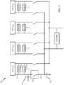
- FIGURE 1 shows an exemplary wireless communication system 100 in which an embodiment of the disclosure may be advantageously employed.
- FIGURE 1 shows three remote units 120, 130, and 150 and two base stations 140. It will be recognized that typical wireless communication systems may have many more remote units and base stations.
- Remote units 120, 130, and 150 include memory devices 125A, 125B and 125C, created according to an embodiment of the disclosure.
- FIGURE 1 shows forward link signals 180 from the base stations 140 and the remote units 120, 130, and 150 and reverse link signals 190 from the remote units 120, 130, and 150 to base stations 140.
- remote unit 120 is shown as a mobile telephone
- remote unit 130 is shown as a portable computer
- remote unit 150 is shown as a fixed location remote unit in a wireless local loop system.
- the remote units may be cell phones, hand-held personal communication systems (PCS) units, portable data units such as personal data assistants, or fixed location data units such as meter reading equipment.
- PCS personal communication systems
- FIGURE 1 illustrates remote units according to the teachings of the disclosure, the disclosure is not limited to these exemplary illustrated units. The disclosure may be suitably employed in any device which includes memory devices fabricated in accordance with the teachings of the disclosure.
- FIGURE 2A is a circuit schematic illustrating a conventional pulsed bit line scheme for improved memory stability.
- a circuit 20 includes a bit cell 21 configured to store data and is coupled to additional circuitry to control the read and write behavior of the circuit 20.
- the bit cell 21 may be a six transistor storage cell.
- a precharge signal, PCH is coupled to a precharge circuit 22.
- the precharge circuit 22 includes a transistor 221 coupled to a bit line, BL, a transistor 222 coupled to an inverse bit line, BLB, and a transistor 223 coupled to both the bit line, BL, and the inverse bit line, BLB.
- a pulse signal, PULSE is coupled to a pull-down circuit 23.
- the pull-down circuit 23 includes a transistor 231 coupled to the bit line, BL, a transistor 232 coupled to the inverse bit line, BLB, and a transistor 233 coupled to both the bit line, BL, and the inverse bit line, BLB.
- FIGURE 2B is a timing diagram illustrating a conventional pulsed bit line scheme for improved memory stability.
- the circuit 20 starts at a time 251 when the precharge signal, PCH, is low and the transistor 221 pulls up the bit line, BL, to a supply voltage, V DD , and the transistor 222 pulls up the inverse bit line, BLB, to the supply voltage, V DD .
- the precharge signal, PCH is high turning off the transistor 221, the transistor 222, and the transistor 223 to disconnect the bit line, BL, and the inverse bit line, BLB, from the supply voltage, V DD .
- a narrow positive pulse is generated on the pulse signal, PULSE.
- the pulse signal, PULSE switches on the transistor 231 and the transistor 232 to couple the bit line, BL, and the inverse bit line, BLB, to a ground 206.
- the transistor 233 switches off to disconnect the bit line, BL, from the inverse bit line, BLB.
- a reduction of voltage occurs on the bit line, BL, and the inverse bit line, BLB.
- the pulse signal, PULSE returns to low so the bit line, BL, and the inverse bit line, BLB, stop reducing voltage.
- the selective precharge technique reduces the bit line voltage to improve read stability without being as sensitive to process, voltage, and temperature variations.
- the bit line voltage is reduced by sharing charge between sections of the bit line that are selectively coupled to enable sharing during the read and write operations.
- SRAM memory devices will be described, the selective precharge technique can be applied to any memory design including, but not limited to, SRAM, DRAM, or MRAM.
- the charge sharing operation is divided into three parts. First, as illustrated in FIGURE 3 , the upper part of the bit line is precharged to V DD while the lower part of the bit line is precharged to GND. Next, as, illustrated in FIGURE 4 , the charge sharing switches are turned on to enable charge sharing between the upper of lower parts of the bit lines. Therefore, the final bit line voltage will be determined by the ratio of capacitance between C BL and C 2 . Finally, as illustrated by FIGURE 5 , charge sharing is disabled for all columns, while the switch remains on for a column selected for a read or write operation.
- FIGURE 3 is a block diagram illustrating initial precharge operation in the exemplary selective precharge technique.
- a block diagram 30 includes an upper bit line 31 along with associated capacitance illustrated by a capacitor 311, with value C BL .
- a lower bit line 33 has associated capacitance illustrated by a capacitor 331, with value C 2 .
- the upper bit line 31 and the lower bit line 33 are coupled to a mux switch 32.
- the mux switch 32 is open during initial precharge to allow the upper bit line 31 to precharge to a supply voltage, V DD , and the lower bit line 33 to precharge to a ground, GND.
- bit cells 34 are coupled to the upper bit line 31. In another embodiment, the bit cells 34 may be coupled to the lower bit line 33.
- FIGURE 4 is a block diagram illustrating charge sharing operation in the exemplary selective precharge technique.
- a block diagram 40 includes the upper bit line 31, the capacitance represented by the capacitor 311, the lower bit line 33, the capacitance represented by the capacitor 331, and the mux switch 32.
- the charge sharing operation occurs by closing the mux switch 32 to couple the upper bit line 31 to the lower bit line 33.
- FIGURE 5 is a block diagram illustrating charge sharing disablement in the exemplary selective precharge technique.
- a block diagram 50 includes the upper bit line 31, the capacitance represented by the capacitor 311, the lower bit line 33, the capacitance represented by the capacitor 331, and the mux switch 32.
- the mux switch 32 opens to disconnect the upper bit line 31 from the lower bit line 33 after charge sharing has completed. This opening disables the charge sharing operation so data may be read from or written to the bit cell 34.
- a mux switch 52 remains closed because a bit cell 54 has been selected for a read or write operation.
- FIGURE 6 is a block diagram illustrating precharge of bit lines to different voltages in the exemplary selective precharge technique according to another embodiment of the disclosure.
- a block diagram 60 includes the upper bit line 31, the capacitance represented by the capacitor 311, the lower bit line 33, the capacitance represented by the capacitor 331, and the mux switch 32.
- the upper bit line 31 is precharged to the supply voltage, V DD
- the lower bit line 33 is precharged to the ground, GND.
- each upper bit line may be precharged to a different voltage.
- an upper bit line 61 is precharged to the ground, GND.
- the upper bit lines and inverse upper bit lines will have a lower final voltage as compared to when all upper bit lines are precharged to the supply voltage, V DD .
- Additional bit lines may be charged to the ground, GND, the supply voltage, V DD , or other supply voltages (not shown) to obtain an appropriate final voltage.
- FIGURE 7 is a timing diagram illustrating selective precharge operation. Operation of selective precharge on an upper bit line, BL U , an inverse upper bit line, BLB U , a lower bit line, BL L , and an inverse lower bit line, BLB L , is controlled by a precharge signal, PRECHG, a mux signal, MUX_STATE, and a charge sharing signal, CH_SH.
- a word line signal, WL enables access to the upper bit line, BL U , inverse upper bit line, BLB U , lower bit line, BL L , and inverse lower bit line BLB L .
- An initial state of the circuit is at a time 711 when the precharge signal, PRECHG, the mux signal, MUX_STATE, the charge sharing signal, CH_SH, and the word line, WL, are low.
- the lower bit line, BL L , and the inverse lower bit line, BLB L are predischarged to ground, and the upper bit line, BL U , and inverse upper bit line, BLB U , are precharged to a supply voltage, V DD .
- the supply voltage level is indicated by the dashed-dotted line.
- the charge sharing signal, CH_SH goes low at the time 713 completing the charge sharing operation.
- the upper bit line, BL U , inverse upper bit line, BLB U , lower bit line, BL L , and inverse lower bit line, BLB L voltages stabilize at the time 713 when the charge sharing operation ends.
- the reductions in voltages of the upper bit line, BLu, and inverse upper bit line, BLB U increase the read stability of the memory.
- the word line, WL goes high indicating a read operation has started.
- the voltage on the upper bit line, BL U , the upper inverse bit line, BLB U , the lower bit line, BL L , and the lower inverse bit line, BLB L discharge towards the ground, GND.
- the precharge signal, PRECHG goes low.
- the upper bit line, BL U , and inverse upper bit line, BLB U are precharged to the supply voltage, V DD
- the lower bit line, BL L , and inverse lower bit line, BLB L are predischarged to ground, GND.
- the mux signal, MUX_STATE went low placing all signals back in their initial state at the time 716.
- FIGURE 8 is a circuit schematic of a circuit for implementing the exemplary selective precharge technique according to one embodiment of the disclosure.
- a circuit 80 includes an upper bit line 85, BL U , and an inverse upper bit line 87, BLB U , configured to accessing bit cells 84. Additionally, the circuit 80 includes a lower bit line 86, BL L , and an inverse lower bit line 88, BLB L . Although the bit cells 84 are shown connected to the upper bit lines 85,87, the bit cells 84 could also be connected to the lower bit lines 86,88.
- a charge-sharing enable circuit 81 configured to activate charge sharing is coupled to the mux signal, MUX_STATE, and the precharge signal, PRECHRG, and outputs a charge sharing signal, CH_SH.
- the charge-sharing enable circuit 81 includes an inverter 812 coupled to the mux signal, MUX_STATE, a NAND gate 814 coupled to the output of the inverter 812 and the precharge signal, PRECHRG, and an inverter 816 coupled to the output of the NAND gate 814.
- the charge-sharing enable circuit 81 illustrated is only one possible combination of logic gates capable of activating charge sharing.
- a precharge circuit 891 is coupled to the upper bit lines 85,87 and a pull down circuit 892 is coupled to the lower bit lines 86,88. The precharge circuit 891 and the pull down circuit 892 may be controlled by the precharge signal, PRECHRG.
- the charge sharing signal, CH_SH, and a select signal, SELn are inputs to a NOR gate 82 for controlling a charge sharing circuit 83.
- the charge sharing circuit 83 is active when the charge sharing signal, CH_SH, is high.
- the select signal, SELn is used to select bit cells for read or write operations. Although only one select signal, SELn, upper bit line, BL U , inverse upper bit line, BLB U , lower bit line, BL L , and inverse lower bit line, BLB L , are shown, many more may be incorporated into the circuit 80. Additionally, many more bit cells may be incorporated into the circuit 80.
- the precharge signal, PRECHG is low and the mux signal, MUX_STATE, is low.
- the output of the charge-sharing enable circuit 81, CH_SH will be low.
- the upper bit lines 85,87 are precharged to the supply voltage, V DD , and the lower bit lines 86,88 are precharged to the ground.
- the output of the charge-sharing enable circuit 81, CH_SH goes high.
- the output of the charge-sharing enable circuit 81, CH_SH goes low. This change causes the charge sharing circuits 83 to decouple the upper bit lines 85,87 from the lower bit lines 86,88, ending charge sharing.
- the bit cells 84 are accessed (in response to the write line signal, WL) and a read or write operation occurs.
- the charge sharing technique improves memory read stability by reducing the bit line voltage from the supply voltage.
- the bit line voltage is reduced by precharging one section of the bit line to a first voltage and a second section of the bit line to a second voltage.
- a charge sharing circuit selectively couples the two sections to reach a bit line voltage between the first and second voltage.
- the final voltage is dependent, in part, on the relative capacitance of the two sections of the bit line, therefore any manufacturing variation in the devices does not affect the operation of the charge sharing.
- the first section is the upper bit line and the second section is the lower bit line.
- One advantage of this disclosure is improved read stability by reducing the bit line voltage.
- a precise voltage level may be chosen for the bit lines.
- SNM static noise margin
- Both accessed bit cells and half-selected bit cells are improved because all the bit lines see lower voltage compared to the bit cell's supply voltage.
- Half-selected bit cells are cells selected by an asserted word line but not selected by its bit lines.
- a second advantage of this disclosure is superior design robustness.
- the disclosure does not depend on the threshold voltage of the transistor and timing of a critical signal.
- a third advantage of this disclosure is process variation tolerance.
- the proposed solution depends on relative capacitance values that do not change with process, voltage, and temperature variation. Bit line voltage will be independent of the process conditions
- a fourth advantage of this disclosure is design flexibility.
- the bit line's voltage value may be changed by selecting which bit line segments to precharge to V DD and which bit line segments to precharge to ground. For example, precharging one bit line or more to ground can allow larger delta values (the change of the bit line from V DD ). For example, if the supply voltage is 1.125 Volts and the upper sections are 1.125 Volts and the lower sections are 1.125 Volts then the final voltage may be 1.125 Volts if all bit lines are precharged to V DD . The delta would be 0 millivolts in this case. However, in the same case if one of the bit lines is predischarged to ground, then the final voltage would be 1.00 Volts. The delta would be 125 milliVolts in this case. Therefore, there is a high degree of flexibility regarding the voltages that bit line sections may be precharged to.
- a fifth advantage of this disclosure is that only one supply voltage is used. This simplifies the top level physical design and verification of the memory.
- the memory device as disclosed may be coupled to a microprocessor or other microelectronic device.
- the memory device may be packaged with the microprocessor and further incorporated into a communications device.
- the memory may be.embedded in a mobile phone or a communications base station.
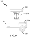
- FIGURE 9 is a block diagram illustrating a design workstation used for circuit, layout, and logic design of the disclosed semiconductor integrated circuit.
- a design workstation 900 includes a hard disk 901 containing operating system software, support files, and design software such as Cadence or OrCAD.
- the design workstation 900 also includes a display to facilitate design of a circuit design 910.
- the circuit design 910 may be the memory circuit as disclosed above.
- a storage medium 904 is provided for tangibly storing the circuit design 910.
- the circuit design 910 may be stored on the storage medium 904 in a file format such as GDSII or GERBER.
- the storage medium 904 may be a CD-ROM, DVD, hard disk, flash memory, or other appropriate device.
- the design workstation 900 includes a drive apparatus 903 for accepting input from or writing output to the storage medium 904.
- Data recorded on the storage medium 904 may specify logic circuit configurations, pattern data for photolithography masks, or mask pattern data for serial write tools such as electron beam lithography.
- the data may further include logic verification data such as timing diagrams or net circuits associated with logic simulations.
- Providing data on the storage medium 904 facilitates the design of the circuit design 910 by decreasing the number of processes for designing semiconductor integrated circuits.
Landscapes
- Engineering & Computer Science (AREA)
- Microelectronics & Electronic Packaging (AREA)
- Computer Hardware Design (AREA)
- Static Random-Access Memory (AREA)
- Semiconductor Memories (AREA)
- Dram (AREA)
- Read Only Memory (AREA)
Claims (13)
- Un dispositif à mémoire comprenant :un moyen de préchargement d'une première section (33) d'une première ligne de bits d'une première cellule binaire (34) d'une première colonne à une première tension,un moyen de préchargement d'une deuxième section (31) de la première ligne de bits d'une première cellule binaire (34) d'une première colonne à une deuxième tension, où une deuxième tension est différente de la première tension,un moyen de préchargement d'une première section d'une deuxième ligne de bits d'une deuxième cellule binaire d'une deuxième colonne à la première tension,un moyen de préchargement d'une deuxième section (61) de la deuxième ligne de bits de la deuxième cellule binaire de la deuxième colonne à la première tension, où la première section de la deuxième ligne de bits est couplée à la première section de la première ligne de bits, etun moyen de partage d'une charge entre la première section de la première ligne de bits, la deuxième section de la première ligne de bits, la première section de la deuxième ligne de bits et la deuxième section de la deuxième ligne de bits, où le moyen de partage d'une charge est configuré en outre de façon àcoupler la première section de la première ligne de bits à la deuxième section de la première ligne de bits au cours d'une opération de lecture ou d'écriture lorsque la première cellule binaire est sélectionnée pour l'opération de lecture ou d'écriture.
- Le dispositif à mémoire selon la Revendication 1, où le moyen de partage comprend :
un circuit de partage de charge couplé de manière sélective à la première section de la première ligne de bits et à la deuxième section de la première ligne de bits, dans lequel le circuit de partage de charge est configuré de façon à coupler et découpler la première section de la première ligne de bits à/de la deuxième section de la première ligne de bits. - Le dispositif à mémoire selon la Revendication 1, où la première section de la première ligne de bits est prédéchargée vers la terre et la deuxième section de la première ligne de bits est préchargée à une tension d'alimentation.
- Le dispositif à mémoire selon la Revendication 1, comprenant en outre un circuit d'activation de partage de charge configuré de façon à activer le circuit de partage de charge lorsqu'un circuit de préchargement est inactif et qu'un signal de multiplexage indique un partage de charge.
- Le dispositif à mémoire selon la Revendication 1, où la première cellule binaire (34) est couplée à la deuxième section de la première ligne de bits.
- Le dispositif à mémoire selon la Revendication 2, où le circuit de partage de charge est couplé de manière sélective à la première section de la deuxième ligne de bits et à la deuxième section de la deuxième ligne de bits et est configuré de façon à coupler et découpler la première section de la deuxième ligne de bits à/de la deuxième section de la deuxième ligne de bits.
- Le dispositif à mémoire selon la Revendication 1, dans lequel le dispositif à mémoire est couplé à un microprocesseur, et dans lequel le dispositif à mémoire et le microprocesseur sont intégrés à un dispositif de communication.
- Un procédé d'actionnement d'un dispositif à mémoire possédant une pluralité de lignes de bits comprenant une première section et une deuxième section comprenant :le préchargement de la première section (33) d'une première ligne de bits d'une première cellule binaire (34) d'une première colonne à une première tension,le préchargement de la deuxième section (31) de la première ligne de bits de la première cellule binaire de la première colonne à une deuxième tension, la deuxième tension étant différente de la première tension,le préchargement d'une première section d'une deuxième ligne de bits d'une deuxième cellule binaire d'une deuxième colonne à la première tension,le préchargement d'une deuxième section (61) de la deuxième ligne de bits de la deuxième cellule binaire de la deuxième colonne à la première tension, où la première section de la deuxième ligne de bits est couplée à la première section de la première ligne de bits, le partage d'une charge entre la première section de la première ligne de bits, la deuxième section de la première ligne de bits, la première section de la deuxième ligne de bits et la deuxième section de la deuxième ligne de bits de façon à obtenir une tension finale entre la première tension et la deuxième tension, etle couplage de la première section de la première ligne de bits à la deuxième section de la première ligne de bits au cours d'une opération de lecture ou d'écriture lorsque la première cellule binaire est sélectionnée pour l'opération de lecture ou d'écriture.
- Le procédé selon la Revendication 8, dans lequel la tension finale est déterminée, au moins en partie, par une capacité de la première section de la première ligne de bits et une capacité de la deuxième section de la première ligne de bits.
- Le procédé selon la Revendication 8, dans lequel le préchargement de la première section de la première ligne de bits comprend le préchargement de la première section de la première ligne de bits à une tension de masse et le préchargement de la deuxième section de la première ligne de bits comprend le préchargement de la deuxième section de la première ligne de bits à une tension d'alimentation.
- Le procédé selon la Revendication 8, comprenant en outre : le préchargement d'une première section d'une deuxième ligne de bits et d'une deuxième section d'une deuxième ligne de bits à la première tension.
- Le procédé selon la Revendication 8, dans lequel le partage de charge se déroule en fonction d'un signal d'état de multiplexage (MUX_STATE) lorsqu'un circuit de préchargement est inactif.
- Le procédé selon la Revendication 8, comprenant en outre : la conservation en mémoire dans le dispositif à mémoire de données relatives à des communications.
Applications Claiming Priority (3)
| Application Number | Priority Date | Filing Date | Title |
|---|---|---|---|
| US1403807P | 2007-12-15 | 2007-12-15 | |
| PCT/US2008/086829 WO2009079455A1 (fr) | 2007-12-15 | 2008-12-15 | Amélioration de stabilité de lecture de mémoire au moyen de la précharge sélective de sections de ligne de bits |
| US12/334,817 US8223567B2 (en) | 2007-12-15 | 2008-12-15 | Memory read stability using selective precharge |
Publications (2)
| Publication Number | Publication Date |
|---|---|
| EP2243140A1 EP2243140A1 (fr) | 2010-10-27 |
| EP2243140B1 true EP2243140B1 (fr) | 2018-06-06 |
Family
ID=40456819
Family Applications (1)
| Application Number | Title | Priority Date | Filing Date |
|---|---|---|---|
| EP08862363.2A Active EP2243140B1 (fr) | 2007-12-15 | 2008-12-15 | Amélioration de stabilité de lecture de mémoire au moyen de la précharge sélective de sections de ligne de bits |
Country Status (10)
| Country | Link |
|---|---|
| US (1) | US8223567B2 (fr) |
| EP (1) | EP2243140B1 (fr) |
| JP (2) | JP5855342B2 (fr) |
| KR (1) | KR101251360B1 (fr) |
| CN (1) | CN101919003A (fr) |
| BR (1) | BRPI0820983B8 (fr) |
| CA (1) | CA2709400C (fr) |
| MX (1) | MX2010006666A (fr) |
| RU (1) | RU2444073C1 (fr) |
| WO (1) | WO2009079455A1 (fr) |
Families Citing this family (28)
| Publication number | Priority date | Publication date | Assignee | Title |
|---|---|---|---|---|
| JP5855342B2 (ja) * | 2007-12-15 | 2016-02-09 | クゥアルコム・インコーポレイテッドQualcomm Incorporated | 選択的プリチャージを使用したメモリ読取り安定性の改善 |
| US7881137B2 (en) * | 2008-10-23 | 2011-02-01 | Qualcomm Incorporated | Read assist for memory circuits with different precharge voltage levels for bit line pair |
| US8208290B2 (en) * | 2009-08-26 | 2012-06-26 | Qualcomm Incorporated | System and method to manufacture magnetic random access memory |
| US8375173B2 (en) * | 2009-10-09 | 2013-02-12 | Qualcomm Incorporated | Accessing a multi-channel memory system having non-uniform page sizes |
| US8279659B2 (en) * | 2009-11-12 | 2012-10-02 | Qualcomm Incorporated | System and method of operating a memory device |
| US9385308B2 (en) | 2010-03-26 | 2016-07-05 | Qualcomm Incorporated | Perpendicular magnetic tunnel junction structure |
| US8339882B2 (en) * | 2010-07-12 | 2012-12-25 | Promos Technologies Pte. Ltd. | Dual bit line precharge architecture and method for low power dynamic random access memory (DRAM) integrated circuit devices and devices incorporating embedded DRAM |
| KR101781616B1 (ko) | 2010-07-16 | 2017-09-26 | 삼성전자주식회사 | 어시스트 회로를 포함하는 스태틱 랜덤 액세스 메모리 장치 |
| US9014749B2 (en) | 2010-08-12 | 2015-04-21 | Qualcomm Incorporated | System and method to initiate a housekeeping operation at a mobile device |
| US8638590B2 (en) | 2010-09-28 | 2014-01-28 | Qualcomm Incorporated | Resistance based memory having two-diode access device |
| JP5760829B2 (ja) * | 2011-08-09 | 2015-08-12 | 富士通セミコンダクター株式会社 | スタティックram |
| US8582380B2 (en) * | 2011-12-21 | 2013-11-12 | Micron Technology, Inc. | Systems, circuits, and methods for charge sharing |
| BR122018000153B1 (pt) * | 2011-12-28 | 2021-08-17 | Intel Corporation | Aparelho e método para melhorar o fornecimento de energia em uma memória, como uma memória de acesso aleatório (ram) |
| US8861285B2 (en) | 2012-02-09 | 2014-10-14 | Micron Technology, Inc. | Apparatuses and methods for line charge sharing |
| US9224453B2 (en) * | 2013-03-13 | 2015-12-29 | Qualcomm Incorporated | Write-assisted memory with enhanced speed |
| US9123430B2 (en) * | 2013-06-14 | 2015-09-01 | Sandisk 3D Llc | Differential current sense amplifier and method for non-volatile memory |
| US9508405B2 (en) | 2013-10-03 | 2016-11-29 | Stmicroelectronics International N.V. | Method and circuit to enable wide supply voltage difference in multi-supply memory |
| KR102173431B1 (ko) * | 2014-05-02 | 2020-11-03 | 삼성전자주식회사 | 동작 전류가 감소된 메모리 장치 |
| GB2525904B (en) | 2014-05-08 | 2018-05-09 | Surecore Ltd | Memory unit |
| US9672898B1 (en) | 2016-08-15 | 2017-06-06 | Samsung Electronics Co., Ltd. | Read column select negative boost driver circuit, system, and method |
| US10431278B2 (en) * | 2017-08-14 | 2019-10-01 | Qualcomm Incorporated | Dynamically controlling voltage for access operations to magneto-resistive random access memory (MRAM) bit cells to account for ambient temperature |
| CN109817260B (zh) * | 2017-11-20 | 2021-02-09 | 中芯国际集成电路制造(上海)有限公司 | 位线预置电路、读操作电路、sram和方法 |
| JP7236574B2 (ja) * | 2018-02-27 | 2023-03-09 | ラピスセミコンダクタ株式会社 | 半導体装置及び半導体メモリのデータ読出方法 |
| CN108665931B (zh) * | 2018-05-21 | 2021-04-13 | 上海华力集成电路制造有限公司 | 位线预降压器 |
| US10657089B2 (en) | 2018-07-30 | 2020-05-19 | Texas Instruments Incorporated | Embedded universal serial bus 2 repeater |
| US11386036B2 (en) * | 2018-08-06 | 2022-07-12 | Texas Instruments Incorporated | Embedded universal serial bus 2 repeater |
| US11100964B1 (en) | 2020-02-10 | 2021-08-24 | Taiwan Semiconductor Manufacturing Company Limited | Multi-stage bit line pre-charge |
| US11532351B2 (en) * | 2020-05-08 | 2022-12-20 | Taiwan Semiconductor Manufacturing Company, Ltd. | Memory device with additional write bit lines |
Citations (1)
| Publication number | Priority date | Publication date | Assignee | Title |
|---|---|---|---|---|
| JPH03102698A (ja) * | 1989-09-14 | 1991-04-30 | Hitachi Ltd | 半導体記憶装置 |
Family Cites Families (13)
| Publication number | Priority date | Publication date | Assignee | Title |
|---|---|---|---|---|
| JP2615011B2 (ja) * | 1986-06-13 | 1997-05-28 | 株式会社日立製作所 | 半導体記憶回路 |
| JPH0821236B2 (ja) * | 1987-01-26 | 1996-03-04 | 株式会社日立製作所 | 半導体記憶装置 |
| RU2060564C1 (ru) * | 1993-06-24 | 1996-05-20 | Научно-исследовательский институт точных приборов | Усилитель считывания для запоминающего устройства |
| JPH10222985A (ja) * | 1998-03-09 | 1998-08-21 | Hitachi Ltd | 半導体記憶装置 |
| US6282137B1 (en) * | 1999-09-14 | 2001-08-28 | Agere Systems Guardian Corp. | SRAM method and apparatus |
| JP4087570B2 (ja) * | 2001-01-19 | 2008-05-21 | 富士通株式会社 | 半導体メモリおよびその制御方法 |
| CA2345845C (fr) * | 2001-04-30 | 2012-03-27 | Mosaid Technologies Incorporated | Precharge de lignes de bits |
| JP4370100B2 (ja) * | 2003-01-10 | 2009-11-25 | パナソニック株式会社 | 半導体記憶装置 |
| US6934213B2 (en) * | 2003-06-11 | 2005-08-23 | Artisan Components, Inc. | Method and apparatus for reducing write power consumption in random access memories |
| US7009886B1 (en) * | 2004-07-19 | 2006-03-07 | Silicon Storage Technology, Inc. | Integrated circuit memory device with bit line pre-charging based upon partial address decoding |
| US7573775B2 (en) * | 2006-02-09 | 2009-08-11 | Fujitsu Limited | Setting threshold voltages of cells in a memory block to reduce leakage in the memory block |
| JP5855342B2 (ja) * | 2007-12-15 | 2016-02-09 | クゥアルコム・インコーポレイテッドQualcomm Incorporated | 選択的プリチャージを使用したメモリ読取り安定性の改善 |
| US7881137B2 (en) * | 2008-10-23 | 2011-02-01 | Qualcomm Incorporated | Read assist for memory circuits with different precharge voltage levels for bit line pair |
-
2008
- 2008-12-15 JP JP2010538225A patent/JP5855342B2/ja active Active
- 2008-12-15 MX MX2010006666A patent/MX2010006666A/es active IP Right Grant
- 2008-12-15 CN CN2008801250308A patent/CN101919003A/zh active Pending
- 2008-12-15 WO PCT/US2008/086829 patent/WO2009079455A1/fr not_active Ceased
- 2008-12-15 US US12/334,817 patent/US8223567B2/en active Active
- 2008-12-15 KR KR1020107015737A patent/KR101251360B1/ko not_active Expired - Fee Related
- 2008-12-15 RU RU2010129245/08A patent/RU2444073C1/ru active
- 2008-12-15 BR BRPI0820983A patent/BRPI0820983B8/pt active IP Right Grant
- 2008-12-15 EP EP08862363.2A patent/EP2243140B1/fr active Active
- 2008-12-15 CA CA2709400A patent/CA2709400C/fr not_active Expired - Fee Related
-
2015
- 2015-06-02 JP JP2015112568A patent/JP2015207336A/ja not_active Withdrawn
Patent Citations (1)
| Publication number | Priority date | Publication date | Assignee | Title |
|---|---|---|---|---|
| JPH03102698A (ja) * | 1989-09-14 | 1991-04-30 | Hitachi Ltd | 半導体記憶装置 |
Also Published As
| Publication number | Publication date |
|---|---|
| JP2011507139A (ja) | 2011-03-03 |
| KR20100092971A (ko) | 2010-08-23 |
| BRPI0820983B8 (pt) | 2021-08-10 |
| BRPI0820983A2 (pt) | 2015-10-13 |
| BRPI0820983B1 (pt) | 2019-06-25 |
| EP2243140A1 (fr) | 2010-10-27 |
| RU2010129245A (ru) | 2012-01-20 |
| CN101919003A (zh) | 2010-12-15 |
| JP5855342B2 (ja) | 2016-02-09 |
| US20090154274A1 (en) | 2009-06-18 |
| JP2015207336A (ja) | 2015-11-19 |
| CA2709400A1 (fr) | 2009-06-25 |
| CA2709400C (fr) | 2013-12-17 |
| MX2010006666A (es) | 2010-09-07 |
| US8223567B2 (en) | 2012-07-17 |
| KR101251360B1 (ko) | 2013-04-05 |
| RU2444073C1 (ru) | 2012-02-27 |
| BRPI0820983A8 (pt) | 2019-02-05 |
| WO2009079455A1 (fr) | 2009-06-25 |
Similar Documents
| Publication | Publication Date | Title |
|---|---|---|
| US8223567B2 (en) | Memory read stability using selective precharge | |
| US8009459B2 (en) | Circuit for high speed dynamic memory | |
| US8547779B2 (en) | Memory circuits, systems, and method of interleavng accesses thereof | |
| US7561462B2 (en) | Circuit and method for a high speed dynamic RAM | |
| US7313049B2 (en) | Output circuit of a memory and method thereof | |
| EP2988305B1 (fr) | Circuit intégré destiné à stocker des données | |
| US8295099B1 (en) | Dual port memory with write assist | |
| US7817481B2 (en) | Column selectable self-biasing virtual voltages for SRAM write assist | |
| US8213249B2 (en) | Implementing low power data predicting local evaluation for double pumped arrays | |
| US7379347B1 (en) | Memory device and method for performing write operations in such a memory device | |
| US12260904B2 (en) | Memory device with additional write bit lines | |
| US20070183234A1 (en) | Semiconductor memory device having reduced voltage coupling between bit lines | |
| US11264081B1 (en) | Memory circuit, electronic device having the memory circuit, and method of operating memory circuit | |
| US6067264A (en) | High speed semiconductor memory device | |
| US20150162059A1 (en) | Dynamic cascode-managed high-voltage word-line driver circuit | |
| US9087563B2 (en) | SRAM local evaluation and write logic for column selection | |
| US12400708B2 (en) | Memory device and method for reducing active power consumption thereof using address control | |
| JP5867275B2 (ja) | 半導体記憶装置およびそのデータ書き込み方法 | |
| US7221607B1 (en) | Multi-port memory systems and methods for bit line coupling | |
| US20070019461A1 (en) | Methods and apparatus for accessing memory | |
| US6212116B1 (en) | Semiconductor memory device | |
| KR20250145543A (ko) | Bti 인식 메모리 회로 및 그 동작 방법 | |
| ES2685262T3 (es) | Mejora de estabilidad de lectura de memoria usando precarga selectiva de secciones de línea de bits |
Legal Events
| Date | Code | Title | Description |
|---|---|---|---|
| PUAI | Public reference made under article 153(3) epc to a published international application that has entered the european phase |
Free format text: ORIGINAL CODE: 0009012 |
|
| 17P | Request for examination filed |
Effective date: 20100707 |
|
| AK | Designated contracting states |
Kind code of ref document: A1 Designated state(s): AT BE BG CH CY CZ DE DK EE ES FI FR GB GR HR HU IE IS IT LI LT LU LV MC MT NL NO PL PT RO SE SI SK TR |
|
| AX | Request for extension of the european patent |
Extension state: AL BA MK RS |
|
| DAX | Request for extension of the european patent (deleted) | ||
| 17Q | First examination report despatched |
Effective date: 20110214 |
|
| R17C | First examination report despatched (corrected) |
Effective date: 20110214 |
|
| GRAP | Despatch of communication of intention to grant a patent |
Free format text: ORIGINAL CODE: EPIDOSNIGR1 |
|
| STAA | Information on the status of an ep patent application or granted ep patent |
Free format text: STATUS: GRANT OF PATENT IS INTENDED |
|
| INTG | Intention to grant announced |
Effective date: 20171220 |
|
| GRAS | Grant fee paid |
Free format text: ORIGINAL CODE: EPIDOSNIGR3 |
|
| GRAA | (expected) grant |
Free format text: ORIGINAL CODE: 0009210 |
|
| STAA | Information on the status of an ep patent application or granted ep patent |
Free format text: STATUS: THE PATENT HAS BEEN GRANTED |
|
| AK | Designated contracting states |
Kind code of ref document: B1 Designated state(s): AT BE BG CH CY CZ DE DK EE ES FI FR GB GR HR HU IE IS IT LI LT LU LV MC MT NL NO PL PT RO SE SI SK TR |
|
| REG | Reference to a national code |
Ref country code: GB Ref legal event code: FG4D |
|
| REG | Reference to a national code |
Ref country code: CH Ref legal event code: EP Ref country code: AT Ref legal event code: REF Ref document number: 1006946 Country of ref document: AT Kind code of ref document: T Effective date: 20180615 |
|
| REG | Reference to a national code |
Ref country code: IE Ref legal event code: FG4D |
|
| REG | Reference to a national code |
Ref country code: DE Ref legal event code: R096 Ref document number: 602008055563 Country of ref document: DE |
|
| REG | Reference to a national code |
Ref country code: NL Ref legal event code: FP |
|
| REG | Reference to a national code |
Ref country code: ES Ref legal event code: FG2A Ref document number: 2685262 Country of ref document: ES Kind code of ref document: T3 Effective date: 20181008 |
|
| REG | Reference to a national code |
Ref country code: LT Ref legal event code: MG4D |
|
| PG25 | Lapsed in a contracting state [announced via postgrant information from national office to epo] |
Ref country code: SE Free format text: LAPSE BECAUSE OF FAILURE TO SUBMIT A TRANSLATION OF THE DESCRIPTION OR TO PAY THE FEE WITHIN THE PRESCRIBED TIME-LIMIT Effective date: 20180606 Ref country code: CY Free format text: LAPSE BECAUSE OF FAILURE TO SUBMIT A TRANSLATION OF THE DESCRIPTION OR TO PAY THE FEE WITHIN THE PRESCRIBED TIME-LIMIT Effective date: 20180606 Ref country code: BG Free format text: LAPSE BECAUSE OF FAILURE TO SUBMIT A TRANSLATION OF THE DESCRIPTION OR TO PAY THE FEE WITHIN THE PRESCRIBED TIME-LIMIT Effective date: 20180906 Ref country code: NO Free format text: LAPSE BECAUSE OF FAILURE TO SUBMIT A TRANSLATION OF THE DESCRIPTION OR TO PAY THE FEE WITHIN THE PRESCRIBED TIME-LIMIT Effective date: 20180906 Ref country code: LT Free format text: LAPSE BECAUSE OF FAILURE TO SUBMIT A TRANSLATION OF THE DESCRIPTION OR TO PAY THE FEE WITHIN THE PRESCRIBED TIME-LIMIT Effective date: 20180606 |
|
| PG25 | Lapsed in a contracting state [announced via postgrant information from national office to epo] |
Ref country code: GR Free format text: LAPSE BECAUSE OF FAILURE TO SUBMIT A TRANSLATION OF THE DESCRIPTION OR TO PAY THE FEE WITHIN THE PRESCRIBED TIME-LIMIT Effective date: 20180907 Ref country code: HR Free format text: LAPSE BECAUSE OF FAILURE TO SUBMIT A TRANSLATION OF THE DESCRIPTION OR TO PAY THE FEE WITHIN THE PRESCRIBED TIME-LIMIT Effective date: 20180606 Ref country code: LV Free format text: LAPSE BECAUSE OF FAILURE TO SUBMIT A TRANSLATION OF THE DESCRIPTION OR TO PAY THE FEE WITHIN THE PRESCRIBED TIME-LIMIT Effective date: 20180606 |
|
| REG | Reference to a national code |
Ref country code: AT Ref legal event code: MK05 Ref document number: 1006946 Country of ref document: AT Kind code of ref document: T Effective date: 20180606 |
|
| PG25 | Lapsed in a contracting state [announced via postgrant information from national office to epo] |
Ref country code: RO Free format text: LAPSE BECAUSE OF FAILURE TO SUBMIT A TRANSLATION OF THE DESCRIPTION OR TO PAY THE FEE WITHIN THE PRESCRIBED TIME-LIMIT Effective date: 20180606 Ref country code: CZ Free format text: LAPSE BECAUSE OF FAILURE TO SUBMIT A TRANSLATION OF THE DESCRIPTION OR TO PAY THE FEE WITHIN THE PRESCRIBED TIME-LIMIT Effective date: 20180606 Ref country code: AT Free format text: LAPSE BECAUSE OF FAILURE TO SUBMIT A TRANSLATION OF THE DESCRIPTION OR TO PAY THE FEE WITHIN THE PRESCRIBED TIME-LIMIT Effective date: 20180606 Ref country code: EE Free format text: LAPSE BECAUSE OF FAILURE TO SUBMIT A TRANSLATION OF THE DESCRIPTION OR TO PAY THE FEE WITHIN THE PRESCRIBED TIME-LIMIT Effective date: 20180606 Ref country code: IS Free format text: LAPSE BECAUSE OF FAILURE TO SUBMIT A TRANSLATION OF THE DESCRIPTION OR TO PAY THE FEE WITHIN THE PRESCRIBED TIME-LIMIT Effective date: 20181006 Ref country code: PL Free format text: LAPSE BECAUSE OF FAILURE TO SUBMIT A TRANSLATION OF THE DESCRIPTION OR TO PAY THE FEE WITHIN THE PRESCRIBED TIME-LIMIT Effective date: 20180606 Ref country code: SK Free format text: LAPSE BECAUSE OF FAILURE TO SUBMIT A TRANSLATION OF THE DESCRIPTION OR TO PAY THE FEE WITHIN THE PRESCRIBED TIME-LIMIT Effective date: 20180606 |
|
| REG | Reference to a national code |
Ref country code: HU Ref legal event code: AG4A Ref document number: E040131 Country of ref document: HU |
|
| REG | Reference to a national code |
Ref country code: DE Ref legal event code: R097 Ref document number: 602008055563 Country of ref document: DE |
|
| PLBE | No opposition filed within time limit |
Free format text: ORIGINAL CODE: 0009261 |
|
| STAA | Information on the status of an ep patent application or granted ep patent |
Free format text: STATUS: NO OPPOSITION FILED WITHIN TIME LIMIT |
|
| 26N | No opposition filed |
Effective date: 20190307 |
|
| PG25 | Lapsed in a contracting state [announced via postgrant information from national office to epo] |
Ref country code: SI Free format text: LAPSE BECAUSE OF FAILURE TO SUBMIT A TRANSLATION OF THE DESCRIPTION OR TO PAY THE FEE WITHIN THE PRESCRIBED TIME-LIMIT Effective date: 20180606 Ref country code: DK Free format text: LAPSE BECAUSE OF FAILURE TO SUBMIT A TRANSLATION OF THE DESCRIPTION OR TO PAY THE FEE WITHIN THE PRESCRIBED TIME-LIMIT Effective date: 20180606 |
|
| REG | Reference to a national code |
Ref country code: CH Ref legal event code: PL |
|
| PG25 | Lapsed in a contracting state [announced via postgrant information from national office to epo] |
Ref country code: MC Free format text: LAPSE BECAUSE OF FAILURE TO SUBMIT A TRANSLATION OF THE DESCRIPTION OR TO PAY THE FEE WITHIN THE PRESCRIBED TIME-LIMIT Effective date: 20180606 Ref country code: LU Free format text: LAPSE BECAUSE OF NON-PAYMENT OF DUE FEES Effective date: 20181215 |
|
| REG | Reference to a national code |
Ref country code: IE Ref legal event code: MM4A |
|
| REG | Reference to a national code |
Ref country code: BE Ref legal event code: MM Effective date: 20181231 |
|
| PG25 | Lapsed in a contracting state [announced via postgrant information from national office to epo] |
Ref country code: IE Free format text: LAPSE BECAUSE OF NON-PAYMENT OF DUE FEES Effective date: 20181215 |
|
| PG25 | Lapsed in a contracting state [announced via postgrant information from national office to epo] |
Ref country code: BE Free format text: LAPSE BECAUSE OF NON-PAYMENT OF DUE FEES Effective date: 20181231 |
|
| PG25 | Lapsed in a contracting state [announced via postgrant information from national office to epo] |
Ref country code: LI Free format text: LAPSE BECAUSE OF NON-PAYMENT OF DUE FEES Effective date: 20181231 Ref country code: CH Free format text: LAPSE BECAUSE OF NON-PAYMENT OF DUE FEES Effective date: 20181231 |
|
| PG25 | Lapsed in a contracting state [announced via postgrant information from national office to epo] |
Ref country code: MT Free format text: LAPSE BECAUSE OF NON-PAYMENT OF DUE FEES Effective date: 20181215 |
|
| PG25 | Lapsed in a contracting state [announced via postgrant information from national office to epo] |
Ref country code: TR Free format text: LAPSE BECAUSE OF FAILURE TO SUBMIT A TRANSLATION OF THE DESCRIPTION OR TO PAY THE FEE WITHIN THE PRESCRIBED TIME-LIMIT Effective date: 20180606 |
|
| PG25 | Lapsed in a contracting state [announced via postgrant information from national office to epo] |
Ref country code: PT Free format text: LAPSE BECAUSE OF FAILURE TO SUBMIT A TRANSLATION OF THE DESCRIPTION OR TO PAY THE FEE WITHIN THE PRESCRIBED TIME-LIMIT Effective date: 20180606 |
|
| PGFP | Annual fee paid to national office [announced via postgrant information from national office to epo] |
Ref country code: NL Payment date: 20241114 Year of fee payment: 17 |
|
| PGFP | Annual fee paid to national office [announced via postgrant information from national office to epo] |
Ref country code: DE Payment date: 20241111 Year of fee payment: 17 |
|
| PGFP | Annual fee paid to national office [announced via postgrant information from national office to epo] |
Ref country code: FI Payment date: 20241126 Year of fee payment: 17 |
|
| PGFP | Annual fee paid to national office [announced via postgrant information from national office to epo] |
Ref country code: GB Payment date: 20241114 Year of fee payment: 17 |
|
| PGFP | Annual fee paid to national office [announced via postgrant information from national office to epo] |
Ref country code: FR Payment date: 20241111 Year of fee payment: 17 |
|
| PGFP | Annual fee paid to national office [announced via postgrant information from national office to epo] |
Ref country code: HU Payment date: 20241204 Year of fee payment: 17 |
|
| PGFP | Annual fee paid to national office [announced via postgrant information from national office to epo] |
Ref country code: IT Payment date: 20241212 Year of fee payment: 17 |
|
| PGFP | Annual fee paid to national office [announced via postgrant information from national office to epo] |
Ref country code: ES Payment date: 20250116 Year of fee payment: 17 |