EP2263251B1 - Verfahren zur übertragung mit einem ferroelektrischen substrat - Google Patents
Verfahren zur übertragung mit einem ferroelektrischen substrat Download PDFInfo
- Publication number
- EP2263251B1 EP2263251B1 EP09731294A EP09731294A EP2263251B1 EP 2263251 B1 EP2263251 B1 EP 2263251B1 EP 09731294 A EP09731294 A EP 09731294A EP 09731294 A EP09731294 A EP 09731294A EP 2263251 B1 EP2263251 B1 EP 2263251B1
- Authority
- EP
- European Patent Office
- Prior art keywords
- substrate
- layer
- components
- transfer
- stage
- Prior art date
- Legal status (The legal status is an assumption and is not a legal conclusion. Google has not performed a legal analysis and makes no representation as to the accuracy of the status listed.)
- Not-in-force
Links
Images




Classifications
-
- H—ELECTRICITY
- H10—SEMICONDUCTOR DEVICES; ELECTRIC SOLID-STATE DEVICES NOT OTHERWISE PROVIDED FOR
- H10P—GENERIC PROCESSES OR APPARATUS FOR THE MANUFACTURE OR TREATMENT OF DEVICES COVERED BY CLASS H10
- H10P10/00—Bonding of wafers, substrates or parts of devices
- H10P10/12—Bonding of semiconductor wafers or semiconductor substrates to semiconductor wafers or semiconductor substrates
- H10P10/128—Bonding of semiconductor wafers or semiconductor substrates to semiconductor wafers or semiconductor substrates by direct semiconductor to semiconductor bonding
-
- Y—GENERAL TAGGING OF NEW TECHNOLOGICAL DEVELOPMENTS; GENERAL TAGGING OF CROSS-SECTIONAL TECHNOLOGIES SPANNING OVER SEVERAL SECTIONS OF THE IPC; TECHNICAL SUBJECTS COVERED BY FORMER USPC CROSS-REFERENCE ART COLLECTIONS [XRACs] AND DIGESTS
- Y10—TECHNICAL SUBJECTS COVERED BY FORMER USPC
- Y10S—TECHNICAL SUBJECTS COVERED BY FORMER USPC CROSS-REFERENCE ART COLLECTIONS [XRACs] AND DIGESTS
- Y10S414/00—Material or article handling
- Y10S414/135—Associated with semiconductor wafer handling
-
- Y—GENERAL TAGGING OF NEW TECHNOLOGICAL DEVELOPMENTS; GENERAL TAGGING OF CROSS-SECTIONAL TECHNOLOGIES SPANNING OVER SEVERAL SECTIONS OF THE IPC; TECHNICAL SUBJECTS COVERED BY FORMER USPC CROSS-REFERENCE ART COLLECTIONS [XRACs] AND DIGESTS
- Y10—TECHNICAL SUBJECTS COVERED BY FORMER USPC
- Y10S—TECHNICAL SUBJECTS COVERED BY FORMER USPC CROSS-REFERENCE ART COLLECTIONS [XRACs] AND DIGESTS
- Y10S414/00—Material or article handling
- Y10S414/135—Associated with semiconductor wafer handling
- Y10S414/141—Associated with semiconductor wafer handling includes means for gripping wafer
Definitions
- the invention relates to substrate transfer techniques, which are used in particular in microelectronics.
- a temporary support also called "handle”.
- On such a support can be temporarily fixed one or more components, which can then be transferred to another support, definitive.
- the holder or the handle substrate can then be reused for another transfer.
- Step a) uses the internal field of the ferroelectric material substrate, which is intrinsically charged.
- the ferroelectric material of the first substrate is LTO (LiTaO 3 ) or a material of the same structure as LTO, such as LiNbO 3 , BaTiO 3 , or SrTiO 3 , or LaAlO 3 , or LiAlO 3 , or any other ferroelectric material.
- One or more of said components, or said layer may have undergone, before step a), or undergo, between step a) and step b), a treatment by etching, and / or ion implantation, and / or or deposit and / or thermal.
- an embrittlement zone is produced in at least one of said components or said layer, along which a fracture is made in step c).
- an embrittlement zone is formed in at least one of said components or of said layer, along which a fracture is made between step a) and step b).
- the layer reported in step c) may be thicker or thicker.
- a layer on the surface of the ferroelectric material to promote bonding, for example a layer of silicon oxide SiO 2 or a polymer (PDMS, BCB) with low or very low resistance.
- a layer of silicon oxide SiO 2 or a polymer (PDMS, BCB) with low or very low resistance.
- the transfer operation can be carried out several times, in particular using the same first ferroelectric substrate, a layer being thus reported, or components being thus carried over, on a layer already reported, or on components already reported, which makes it possible to produce stacks or stages of components on the same second substrate.
- the transfer of the first stage can be realized with the same substrate, in a ferroelectric material, as the transfer of the second stage.
- At least the first substrate may include alignment marks.
- a method according to the invention allows a new mode of handling a film or vignettes, having a temporary support, by electrostatic bonding.
- a first example of a process according to the invention will be given in connection with the Figures 1A-1C , starting from a first solid or thin-film substrate 2, made of a ferroelectric material, for example LiTaO 3 .
- a ferroelectric material for example LiTaO 3 .
- This type of material, as well as the other usable ferroelectric materials mentioned above, have an intrinsic polarization that can be exploited in the context of the present invention.
- Components 8, 10, for example of the "vignette” type are deposited on this substrate 2 ( Figure 1A ).
- These components are for example substrates of semiconductor materials, with or without circuits. They are mainly based on silicon or germanium or AsGa or InP or other materials.
- the reference 30 designates any alignment marks on the substrate 2, which will subsequently enable good alignment on a second substrate 20, or transfer substrate, especially if alignment marks are also provided on the second substrate 20 .
- These components 8, 10 can be of any size, for example they are chips. Each side of one of these components can measure between a few micrometers and several millimeters or several centimeters, for example between 1 micron or 5 microns and 1 mm or 5 mm or 5 cm.
- each component may be such that it can not be handled individually.
- its thickness can be of the order of a few nanometers to a few tens of nanometers, for example between 5 nm or 10 nm and 50 nm. This is the case, in particular, of some vignettes or some chips.
- a transfer technique according to the invention makes this vignette or this chip manipulable.
- the thickness of the components may also be greater, for example 750 ⁇ m or more, or even several millimeters.
- the surfaces 8 ', 10' ( Figure 1A ) the various components can be arranged substantially at the same height h relative to the surface 2 'of the first substrate 2 on which these components are deposited.
- these surfaces 8 'and 10' may not be at the same height h with respect to this same surface 2 'of the substrate 2.
- at least one of the components comprises at least one surface in a material having elasticity or compliant, for example a polymer. It has been shown by Jourdain et al. BCB Collective Hybrid Bonding for 3D-Stacking Conference on Wafer Bonding for MEMS Technologies and Wafer Level Integration, 2007 that a compliant polymer layer, for example BCB, can accept differences in height of over 3 mm during postponements.
- the components 8, 10 may have undergone a treatment step in order to promote contact or adhesion with the surface 2 'of the first substrate 2, for example a treatment by polishing or by plasma activation.
- This type of treatment may reveal, at the interface between the vignettes and the surface 2 'of the substrate 2, a few monolayers of water.
- each component or label 8, 10 on the first substrate 2 is obtained by the natural electric charges of this substrate 2.
- the spontaneous polarization of the latter can be enhanced by the application of an electric field.
- the components 8, 10 may undergo treatment (s), for example etching, and / or ion implantation, and / or deposition, etc .; in the case of steps with elevation of temperature, the ramp or ramps are chosen, during the thermal budget, so as not to have a polarization inversion phenomenon of the first substrate (ferroelectric); typically one or more ramp (s) lower (s) at 5 ° C / minute.
- the temperature is limited to a value lower than the Curie temperature Tc of the ferroelectric material (for Tantalate, this Curie temperature is equal to approximately 600 ° C. for the Niobate it is approximately 1200 ° C.).
- the components 8, 10 may be prepared for direct or molecular bonding with the surface 20 'of the second transfer substrate 20, optionally after, or in combination with, one or more of the foregoing treatments.
- the set obtained can therefore also, as illustrated on the Figure 1B , then be positioned in front of such a transfer substrate 20, on which the components or the vignettes will be transferred.
- the alignment mark or marks may to help the relative positioning of the two substrates 2, 20.
- the transfer substrate 20 is for example made of silicon or of another semiconductor material, or any other material such as fused silica or quartz.
- the surface 8 ', 10' of the components or vignettes 8, 10 and the surface 20 'of the second substrate 20 are brought into contact with each other ( figure 1C ).
- the adhesion of the vignettes on the latter is of the molecular bonding type, which makes it possible to hold them on the support or the second substrate 20, more firmly than they are, by electrostatic effect, on the first substrate 2.
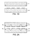
- the latter can be removed ( figure 1D ), the components being transferred to the substrate 20.
- All these steps are preferably carried out at ambient temperature, between 20 ° C. and 30 ° C., for example, except for implantation and / or deposition type treatments.
- the delamination can be obtained by thermal effect, or a thermal effect can assist the mechanical effect to take off the thumbnails of the substrate 2.
- a heating step makes it possible to separate the components 8, 10 from the substrate 2.
- This heating (at a temperature of several hundred ° C., for example between 100 ° C. or 500 ° C. and 1200 ° C., during a duration of between a few minutes and several hours, for example between 1h or 4h and 10h or even 30h) also makes it possible to reinforce the direct or molecular adhesion of the components 8, 10 to the second substrate 20, with respect to the adhesion on the substrate 2.
- an increasing thermal ramp can be applied.
- a thermal ramp greater than 5 ° C / min a charge accumulation in the material of the substrate 2 allows a discharge of the latter and allows or promotes the separation.
- the substrate 2 is delaminated by thermal effect or by combination of mechanical and thermal or electrical and thermal effects.
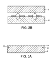
- FIG. 1D Another embodiment of the invention will be explained starting from a second substrate 20, identical or similar to that of the figure 1D , to which a plurality of vignettes 8, 10, forming a first stage, already adheres.
- Components 8 ", 10" for example of the same type as those mentioned above, will be deposited on this first stage.
- the second component stage 8 ", 10" .... can be deposited on the first component stage 8, 10.
- the connection between 8 and 8 “, 10 and 10" may be of the same nature as the prior bond between substrate 20 and components 8, 10, it can also be achieved using glue.
- This transfer of a second stage can be achieved using the same ferroelectric substrate 2 as the transfer of the first stage.
- This variant of the invention makes it possible to produce stacks or stages of components on the second substrate 20.
- a component or a sticker 8 ", 10" is indicated in superposition of each component or sticker 8, 10, but this is not mandatory, the distribution of components or thumbnails 8 ", 10" on the first floor may be different.
- the substrate 2 is shown, as explained above, after having been peeled off or separated by the components 8 ", 10" by thermal effect or by combination of mechanical and thermal or electrical and thermal effects.
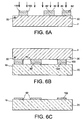
- a second stage can be carried on layer 18 of the figure 3C it may be a component or thumbnail stage 8 ", 10" or a stage having a second layer.
- the 3D figure represents the result of a double transfer, first that of a layer 18, then, on this layer, components 8 ", 10".
- This transfer of a second stage can be carried out using the same ferroelectric substrate 2 as the transfer of the first stage, and according to one of the methods described above.
- Another embodiment uses a substrate fracture method, such as the "Smart Cut TM” method, for example described in the article by B. Aspar and AJ Auberton - Hervé “Silicon Wafer Bonding Technology for VLSI and MEMS Applications”, edited by SS Iyer and AJ Auberton - Herve, 2002, INSPEC, London, Chapter 3, pages 35-52 , or in the documents already mentioned above.
- a substrate fracture method such as the "Smart Cut TM” method, for example described in the article by B. Aspar and AJ Auberton - Hervé “Silicon Wafer Bonding Technology for VLSI and MEMS Applications”, edited by SS Iyer and AJ Auberton - Herve, 2002, INSPEC, London, Chapter 3, pages 35-52 , or in the documents already mentioned above.
- FIGS. 4A to 4D illustrate an example of implementation of such a manufacturing process or thin film transfer. These figures are cross-sectional views.
- the figure 4C illustrates a step of separation, induced by thermal and / or mechanical effect, of the thin layer 21 and the remaining portion 23 of the layer 18, along the weakened zone 19. It remains the structure of the figure 4D that is, the thin layer 21 on the transfer substrate 20.
- FIGS. 5A to 5C it is first carried out in a layer (or a substrate) 18.
- a layer or a substrate
- FIGS. 6A to 6C illustrate an example of implementation of a method of transfer of implanted vignettes.
- the assembly of the vignettes with a ferroelectric substrate 2 is of the type described above in connection with the Figure 1A .
- Thumbnails 80, 100 of the Figure 6A are represented in an enlarged manner compared to those of the Figure 1A .
- the implantation takes place after this assembly with the substrate 2 and an embrittlement zone 80 ', 100' is thus produced in each of the vignettes 80, 100.
- Figure 6B represents the set obtained after transfer of the vignettes of the substrate 2 on the substrate 20, but before the separation step.
- a structure results ( Figure 6C ) having, on the substrate 20 of report, a plurality of thin layers 82, 102, each resulting from the fracture of one of the thumbs 80, 100 along the plane 80 ', 100'.
- FIGS. 7A to 7C illustrate an example of implementation of a method of transfer of implanted vignettes.
- Figure 7B represents the set obtained after transfer of the vignettes of the substrate 2 on the substrate 20, but before the separation step.
- a structure results ( Figure 7C ) having, on the transfer substrate 20, a plurality of thin layers 82, 102, each of which results from the fracture of one of the vignettes 80, 100 along the plane 80 ', 100'.
Landscapes
- Semiconductor Memories (AREA)
- Laminated Bodies (AREA)
- Inorganic Compounds Of Heavy Metals (AREA)
- Inorganic Insulating Materials (AREA)
- Container, Conveyance, Adherence, Positioning, Of Wafer (AREA)
Claims (15)
- Verfahren zum Übertragen einer oder mehrerer erster Komponenten (8,10) oder einer ersten Schicht (18) von einem ersten Substrat (2) auf ein zweites Substrat (20) mit den folgenden Schritten:a) Herstellen eines Kontakts der ersten Komponente(n) oder der ersten Schicht mit einem ersten Substrat (2) aus einem ferroelektrischen Material und ihr Halten an diesem elektrisch geladenen ersten Substrat durch elektrostatische Wirkung,b) Herstellen eines Kontakts dieser Komponenten oder dieser Schicht mit dem zweiten Substrat (20) durch molekulare Adhäsion,c) Trennen oder Abnehmen des ersten Substrats, wobei mindestens ein Teil jeder Komponente oder der Schicht an dem zweiten Substrat bleibt.
- Verfahren nach Anspruch 1, wobei der Abnahmeschritt c) thermisch und/oder mechanisch und/oder elektrostatisch unterstützt wird.
- Verfahren nach Anspruch 2, wobei der Abnahmeschritt c) durch eine Temperaturerhöhung unterstützt wird, zum Beispiel durch Anwenden eines Temperaturanstiegs mit einer Steigung von mehr als 5°C/min.
- Verfahren nach einem der Ansprüche 1 bis 3, wobei der Abnahmeschritt c) unterstützt wird durch einen Unterschied zwischen den Adhäsionskräften der ersten Komponenten oder der ersten Schicht an dem ersten Substrat und an dem zweiten Substrat.
- Verfahren nach einem der Ansprüche 1 bis 4, wobei das erste ferroelektrische Substrat auf intrinsische oder unterstützte Weise geladen ist und/oder aus LiTaO3 oder aus LiNbO3 oder aus BaTiO3 oder aus SrTiO3 oder aus LaAlO3 oder aus LiAlO3 besteht.
- Verfahren nach einem der Ansprüche 1 bis 5, wobei das zweite Substrat (20) zumindest teilweise aus einem Halbleitermaterial, beispielsweise Silizium, oder aus Quarzglas oder aus Quarz besteht und/oder mindestens eine Komponente oder die Schicht (18) zumindest teilweise aus einem Halbleitermaterial besteht.
- Verfahren nach einem der Ansprüche 1 bis 6, wobei eine oder mehrere der Komponenten oder die Schicht einer Ätzbehandlung und/oder Ionenimplantation und/oder Beschichtung und/oder thermischen Behandlung vor dem Schritt a) unterzogen worden sind oder zwischen dem Schritt a) und dem Schritt b) unterzogen werden.
- Verfahren nach Anspruch 7, wobei eine oder mehrere der Komponenten oder die Schicht* einer Behandlung mittels Ionenimplantation vor dem Schritt a) unterzogen worden sind oder zwischen dem Schritt a) und b) unterzogen werden, die in mindestens einer der Komponenten oder in der Schicht eine Sprödigkeitszone (19,100' ,80,80') festlegt, entlang derer während des Schritts c) ein Bruch erfolgt,* einer Behandlung mittels Ionenimplantation vor dem Schritt a) unterzogen worden sind, die in mindestens einer der Komponenten oder in der Schicht eine Sprödigkeitszone (19,100' ,80,80') festlegt, entlang derer zwischen dem Schritt a) und b) ein Bruch erfolgt.
- Verfahren nach einem der Ansprüche 7 oder 8, wobei die thermische Behandlung keine Polarisationsumkehr des Materials des ersten Substrats hervorruft, wobei die thermische Behandlung zum Beispiel durch Anwenden eines Temperaturanstiegs mit einer Steigung von weniger als 5°C/min erfolgt.
- Verfahren nach einem der Ansprüche 1 bis 9, wobei mindestens eine der ersten Komponenten oder die erste Schicht und/oder die Oberfläche (2') des ersten Substrats (2) mindestens einem Behandlungsschritt unterzogen worden sind, um den Kontakt oder die Adhäsion dieser Komponente mit dieser Oberfläche (2') zu begünstigen, und/oder die Oberfläche des zweiten Substrats (20) und/oder die Oberfläche mindestens einer der ersten Komponenten oder der ersten Schicht vor dem Schritt b) einer Vorbehandlung in Hinblick auf das molekulare Kleben unterzogen worden sind.
- Verfahren nach einem der Ansprüche 1 bis 10, wobei die Oberfläche des ersten Substrats aus ferroelektrischem Material eine Klebehilfsschicht aufweist.
- Verfahren nach einem der Ansprüche 1 bis 11, wobei die Oberflächen der Komponenten nicht alle die gleiche Höhe h bezüglich der Oberfläche (2') des ersten Substrats (2) haben, an welchem sie angeordnet sind.
- Verfahren nach einem der Ansprüche 1 bis 12, wobei mindestens eine der Komponenten mindestens eine Oberfläche aus einem nachgiebigen oder elastischen Material aufweist.
- Verfahren zum Übertragen von mindestens zwei aus Komponenten (8,10,8' ,10') und/oder aus einer Schicht (18) bestehenden Stockwerken auf ein zweites Substrat (20) mit den folgenden Schritten:- Übertragen eines aus einer oder mehreren ersten Komponenten (8,10) oder aus einer ersten Schicht (18) bestehenden ersten Stockwerks auf das zweite Substrat (20) nach einem der Ansprüche 1 bis 13 mit Hilfe eines ersten Substrats (2) aus einem ferroelektrischen Material,- anschließendes Übertragen eines aus einer oder mehreren zweiten Komponenten (8" ,10") oder aus einer zweiten Schicht bestehenden zweiten Stockwerks auf das erste Stockwerk.
- Verfahren nach Anspruch 14, wobei das Übertragen eines zweiten Stockwerks erfolgt durch:a') Anordnen und elektrostatisches Halten der einen oder mehreren zweiten Komponenten (8" ,10") oder der zweiten Schicht auf dem ersten Stockwerk mit Hilfe eines elektrisch geladenen Substrats aus einem ferroelektrischen Material,b') Herstellen eines Kontakts und Transferieren dieser Komponenten oder dieser Schicht auf das erste Stockwerk,c') Abnehmen des Substrats aus einem ferroelektrischen Material, wobei die Komponente(n) (8" ,10") oder die zweite Schicht auf dem ersten Stockwerk bleiben.
Applications Claiming Priority (2)
| Application Number | Priority Date | Filing Date | Title |
|---|---|---|---|
| FR0852302A FR2929758B1 (fr) | 2008-04-07 | 2008-04-07 | Procede de transfert a l'aide d'un substrat ferroelectrique |
| PCT/EP2009/054007 WO2009124886A1 (fr) | 2008-04-07 | 2009-04-03 | Procede de transfert a l'aide d'un substrat ferroelectrique |
Publications (2)
| Publication Number | Publication Date |
|---|---|
| EP2263251A1 EP2263251A1 (de) | 2010-12-22 |
| EP2263251B1 true EP2263251B1 (de) | 2012-01-18 |
Family
ID=40118822
Family Applications (1)
| Application Number | Title | Priority Date | Filing Date |
|---|---|---|---|
| EP09731294A Not-in-force EP2263251B1 (de) | 2008-04-07 | 2009-04-03 | Verfahren zur übertragung mit einem ferroelektrischen substrat |
Country Status (6)
| Country | Link |
|---|---|
| US (1) | US8951809B2 (de) |
| EP (1) | EP2263251B1 (de) |
| JP (2) | JP2011517103A (de) |
| AT (1) | ATE542237T1 (de) |
| FR (1) | FR2929758B1 (de) |
| WO (1) | WO2009124886A1 (de) |
Families Citing this family (6)
| Publication number | Priority date | Publication date | Assignee | Title |
|---|---|---|---|---|
| FR2993095B1 (fr) * | 2012-07-03 | 2014-08-08 | Commissariat Energie Atomique | Detachement d’une couche autoportee de silicium <100> |
| DE102015210384A1 (de) | 2015-06-05 | 2016-12-08 | Soitec | Verfahren zur mechanischen Trennung für eine Doppelschichtübertragung |
| WO2017052646A1 (en) * | 2015-09-25 | 2017-03-30 | Intel Corporation | Island transfer for optical, piezo and rf applications |
| FR3078822B1 (fr) * | 2018-03-12 | 2020-02-28 | Soitec | Procede de preparation d’une couche mince de materiau ferroelectrique a base d’alcalin |
| US10926521B2 (en) * | 2018-12-28 | 2021-02-23 | Palo Alto Research Center Incorporated | Method and system for mass assembly of thin film materials |
| FR3160509B1 (fr) * | 2024-03-22 | 2026-03-20 | Soitec Silicon On Insulator | Procédé de fabrication d’une couche ferroélectrique reportée sur un substrat et de polarisation à homogénéité améliorée |
Family Cites Families (56)
| Publication number | Priority date | Publication date | Assignee | Title |
|---|---|---|---|---|
| JPH04100256A (ja) | 1990-08-20 | 1992-04-02 | Fujitsu Ltd | 静電吸着機構を備えた処理装置および被吸着体の離脱方法 |
| JPH04206948A (ja) * | 1990-11-30 | 1992-07-28 | Kyocera Corp | 静電チャック |
| US5536354A (en) | 1993-04-23 | 1996-07-16 | Canon Kabushiki Kaisha | Solid phase bonding method |
| US5467002A (en) | 1993-11-05 | 1995-11-14 | Reliance Medical Products, Inc. | Adjustable chair having programmable control switches |
| JP3076727B2 (ja) * | 1994-10-19 | 2000-08-14 | 東芝機械株式会社 | 試料ホルダの固定装置 |
| US5874747A (en) | 1996-02-05 | 1999-02-23 | Advanced Technology Materials, Inc. | High brightness electroluminescent device emitting in the green to ultraviolet spectrum and method of making the same |
| US5652173A (en) | 1996-05-09 | 1997-07-29 | Philips Electronics North America Corporation | Monolithic microwave circuit with thick conductors |
| US5994207A (en) | 1997-05-12 | 1999-11-30 | Silicon Genesis Corporation | Controlled cleavage process using pressurized fluid |
| FR2775121B1 (fr) | 1998-02-13 | 2000-05-05 | Picogiga Sa | Procede de fabrication de substrats en film mince de materiau semiconducteur, structures epitaxiales de materiau semiconducteur formees sur de tels substrats, et composants obtenus a partir de ces structures |
| US6641662B2 (en) * | 1998-02-17 | 2003-11-04 | The Trustees Of Columbia University In The City Of New York | Method for fabricating ultra thin single-crystal metal oxide wave retarder plates and waveguide polarization mode converter using the same |
| JP3500063B2 (ja) | 1998-04-23 | 2004-02-23 | 信越半導体株式会社 | 剥離ウエーハを再利用する方法および再利用に供されるシリコンウエーハ |
| FR2783254B1 (fr) | 1998-09-10 | 2000-11-10 | France Telecom | Procede d'obtention d'une couche de germanium monocristallin sur un substrat de silicium monocristallin,et produits obtenus |
| JP2000223682A (ja) | 1999-02-02 | 2000-08-11 | Canon Inc | 基体の処理方法及び半導体基板の製造方法 |
| US6350993B1 (en) | 1999-03-12 | 2002-02-26 | International Business Machines Corporation | High speed composite p-channel Si/SiGe heterostructure for field effect devices |
| JP3864612B2 (ja) * | 1999-03-16 | 2007-01-10 | 富士ゼロックス株式会社 | 微小構造体の製造方法および装置 |
| US6468923B1 (en) | 1999-03-26 | 2002-10-22 | Canon Kabushiki Kaisha | Method of producing semiconductor member |
| FR2794893B1 (fr) | 1999-06-14 | 2001-09-14 | France Telecom | Procede de fabrication d'un substrat de silicium comportant une mince couche d'oxyde de silicium ensevelie |
| US6500732B1 (en) | 1999-08-10 | 2002-12-31 | Silicon Genesis Corporation | Cleaving process to fabricate multilayered substrates using low implantation doses |
| FR2797713B1 (fr) | 1999-08-20 | 2002-08-02 | Soitec Silicon On Insulator | Procede de traitement de substrats pour la microelectronique et substrats obtenus par ce procede |
| US6690043B1 (en) | 1999-11-26 | 2004-02-10 | Kabushiki Kaisha Toshiba | Semiconductor device and method of manufacturing the same |
| JP3943782B2 (ja) | 1999-11-29 | 2007-07-11 | 信越半導体株式会社 | 剥離ウエーハの再生処理方法及び再生処理された剥離ウエーハ |
| FR2809867B1 (fr) | 2000-05-30 | 2003-10-24 | Commissariat Energie Atomique | Substrat fragilise et procede de fabrication d'un tel substrat |
| EP1309989B1 (de) | 2000-08-16 | 2007-01-10 | Massachusetts Institute Of Technology | Verfahren für die herstellung eines halbleiterartikels mittels graduellem epitaktischen wachsen |
| JP3589185B2 (ja) | 2000-08-24 | 2004-11-17 | 日亜化学工業株式会社 | 窒化物半導体の成長方法と窒化物半導体基板 |
| US6524935B1 (en) | 2000-09-29 | 2003-02-25 | International Business Machines Corporation | Preparation of strained Si/SiGe on insulator by hydrogen induced layer transfer technique |
| US6890835B1 (en) | 2000-10-19 | 2005-05-10 | International Business Machines Corporation | Layer transfer of low defect SiGe using an etch-back process |
| EP1367150B1 (de) | 2001-02-14 | 2009-08-19 | Toyoda Gosei Co., Ltd. | Verfahren zur herstellung von halbleiterkristallen und halbleiter-leuchtelementen |
| WO2002084631A1 (en) * | 2001-04-11 | 2002-10-24 | Sony Corporation | Element transfer method, element arrangmenet method using the same, and image display apparatus production method |
| FR2823596B1 (fr) | 2001-04-13 | 2004-08-20 | Commissariat Energie Atomique | Substrat ou structure demontable et procede de realisation |
| US20040029365A1 (en) | 2001-05-07 | 2004-02-12 | Linthicum Kevin J. | Methods of fabricating gallium nitride microelectronic layers on silicon layers and gallium nitride microelectronic structures formed thereby |
| DE10156407A1 (de) * | 2001-11-16 | 2003-06-05 | Bosch Gmbh Robert | Haltevorrichtung, insbesondere zum Fixieren eines Halbleiterwafers in einer Plasmaätzvorrichtung, und Verfahren zur Wärmezufuhr oder Wärmeabfuhr von einem Substrat |
| JP3910081B2 (ja) * | 2002-02-26 | 2007-04-25 | 東京応化工業株式会社 | 静電チャック装置及び静電チャック装置からの離脱方法 |
| JP3885939B2 (ja) * | 2002-03-13 | 2007-02-28 | 日本碍子株式会社 | 光導波路デバイスの製造方法 |
| FR2838865B1 (fr) | 2002-04-23 | 2005-10-14 | Soitec Silicon On Insulator | Procede de fabrication d'un substrat avec couche utile sur support de resistivite elevee |
| US6953736B2 (en) | 2002-07-09 | 2005-10-11 | S.O.I.Tec Silicon On Insulator Technologies S.A. | Process for transferring a layer of strained semiconductor material |
| EP1429381B1 (de) | 2002-12-10 | 2011-07-06 | S.O.I.Tec Silicon on Insulator Technologies | Verfahren zur Herstellung eines Verbundmaterials |
| US20090325362A1 (en) | 2003-01-07 | 2009-12-31 | Nabil Chhaimi | Method of recycling an epitaxied donor wafer |
| FR2892228B1 (fr) | 2005-10-18 | 2008-01-25 | Soitec Silicon On Insulator | Procede de recyclage d'une plaquette donneuse epitaxiee |
| WO2004061944A1 (en) | 2003-01-07 | 2004-07-22 | S.O.I.Tec Silicon On Insulator Technologies | Recycling of a wafer comprising a multi-layer structure after taking-off a thin layer |
| EP1588415B1 (de) | 2003-01-07 | 2012-11-28 | Soitec | Recycling durch mechanische mittel eines wafers mit abnehmestruktur nach dem abnehmen einer dünnen schicht davon |
| JP2004247610A (ja) | 2003-02-14 | 2004-09-02 | Canon Inc | 基板の製造方法 |
| JP2004349665A (ja) * | 2003-05-23 | 2004-12-09 | Creative Technology:Kk | 静電チャック |
| FR2855909B1 (fr) * | 2003-06-06 | 2005-08-26 | Soitec Silicon On Insulator | Procede d'obtention concomitante d'au moins une paire de structures comprenant au moins une couche utile reportee sur un substrat |
| FR2858462B1 (fr) | 2003-07-29 | 2005-12-09 | Soitec Silicon On Insulator | Procede d'obtention d'une couche mince de qualite accrue par co-implantation et recuit thermique |
| JP2005064194A (ja) | 2003-08-11 | 2005-03-10 | Seiko Epson Corp | Soi構造を有する半導体基板及びその製造方法及び半導体装置 |
| FR2858875B1 (fr) | 2003-08-12 | 2006-02-10 | Soitec Silicon On Insulator | Procede de realisation de couches minces de materiau semi-conducteur a partir d'une plaquette donneuse |
| FR2867310B1 (fr) | 2004-03-05 | 2006-05-26 | Soitec Silicon On Insulator | Technique d'amelioration de la qualite d'une couche mince prelevee |
| DE102004016073B4 (de) | 2004-03-30 | 2010-12-23 | Texas Instruments Deutschland Gmbh | Verfahren zur Erzeugung eines Impulsausgangssignals aus einem periodischen Sägezahnsignal und einer Referenzspannung, und getakteter Stromwandler |
| US7772088B2 (en) * | 2005-02-28 | 2010-08-10 | Silicon Genesis Corporation | Method for manufacturing devices on a multi-layered substrate utilizing a stiffening backing substrate |
| JP2006324549A (ja) * | 2005-05-20 | 2006-11-30 | Sony Corp | 素子転写装置、素子転写方法および表示装置の製造方法 |
| EP1777735A3 (de) * | 2005-10-18 | 2009-08-19 | S.O.I.Tec Silicon on Insulator Technologies | Verfahren zur Wiederverwendung eines temporären epitaxialen Substrates |
| FR2895562B1 (fr) | 2005-12-27 | 2008-03-28 | Commissariat Energie Atomique | Procede de relaxation d'une couche mince contrainte |
| JP4867373B2 (ja) * | 2006-02-02 | 2012-02-01 | 株式会社ニコン | ウェハホルダ及び半導体装置の製造方法 |
| JP2008041927A (ja) | 2006-08-07 | 2008-02-21 | Shinko Electric Ind Co Ltd | 静電チャックの製造方法 |
| JP2008216869A (ja) * | 2007-03-07 | 2008-09-18 | Matsushita Electric Ind Co Ltd | 光学素子の製造方法 |
| FR2929864B1 (fr) | 2008-04-09 | 2020-02-07 | Commissariat A L'energie Atomique | Auto-assemblage de puces sur un substrat |
-
2008
- 2008-04-07 FR FR0852302A patent/FR2929758B1/fr not_active Expired - Fee Related
-
2009
- 2009-04-03 US US12/936,582 patent/US8951809B2/en not_active Expired - Fee Related
- 2009-04-03 EP EP09731294A patent/EP2263251B1/de not_active Not-in-force
- 2009-04-03 AT AT09731294T patent/ATE542237T1/de active
- 2009-04-03 WO PCT/EP2009/054007 patent/WO2009124886A1/fr not_active Ceased
- 2009-04-03 JP JP2011503408A patent/JP2011517103A/ja active Pending
-
2015
- 2015-01-29 JP JP2015015499A patent/JP2015092632A/ja active Pending
Also Published As
| Publication number | Publication date |
|---|---|
| FR2929758B1 (fr) | 2011-02-11 |
| US8951809B2 (en) | 2015-02-10 |
| WO2009124886A1 (fr) | 2009-10-15 |
| JP2015092632A (ja) | 2015-05-14 |
| ATE542237T1 (de) | 2012-02-15 |
| US20110104829A1 (en) | 2011-05-05 |
| FR2929758A1 (fr) | 2009-10-09 |
| EP2263251A1 (de) | 2010-12-22 |
| JP2011517103A (ja) | 2011-05-26 |
Similar Documents
| Publication | Publication Date | Title |
|---|---|---|
| EP1299905B1 (de) | Verfahren zur trennung einer materialblocks und bildung eines dünnen films | |
| EP1651560B1 (de) | Schichtstruktur und Herstellungsverfahren dafür | |
| EP0950257B1 (de) | Verfahren zur herstellung von einer dünnschicht auf einem träger | |
| EP1497857B1 (de) | Verfahren zur manipulation von halbleiterschichten zum dünnmachen derselben | |
| WO2001011667A1 (fr) | Procede de transfert d'une couche mince comportant une etape de surfragilisation | |
| FR3094573A1 (fr) | Procede de preparation d’une couche mince de materiau ferroelectrique | |
| EP1344249A1 (de) | Verfahren zur herstellung einer gestapelten struktur mit einem an einem zielsubstrat haftenden dünnfilm | |
| EP2586055A1 (de) | Verfahren zur übertragung einer siliziumeinkristall-dünnschicht | |
| FR2809867A1 (fr) | Substrat fragilise et procede de fabrication d'un tel substrat | |
| FR2867307A1 (fr) | Traitement thermique apres detachement smart-cut | |
| FR2860842A1 (fr) | Procede de preparation et d'assemblage de substrats | |
| EP2342745B1 (de) | Verfahren zur herstellung eines hybridsubstrats mit einer eingebetteten elektrisch isolierenden durchgehenden schicht | |
| WO2010049657A1 (fr) | Procede de formation d'une couche monocristalline dans le domaine micro-electronique | |
| EP1364400B9 (de) | Herstellungsverfahren für dünne schichten auf einem spezifischen substrat und anwendung | |
| EP2538438A1 (de) | Verfahren zur Herstellung einer Halbleiteranordnung mit temporären Verkleben | |
| WO2009124886A1 (fr) | Procede de transfert a l'aide d'un substrat ferroelectrique | |
| FR2889887A1 (fr) | Procede de report d'une couche mince sur un support | |
| EP4128330B1 (de) | Verfahren zum produzieren einer gestapelten struktur | |
| FR2858461A1 (fr) | Realisation d'une structure comprenant une couche protegeant contre des traitements chimiques | |
| EP2105958B1 (de) | Verfahren zur Herstellung einer vorgespannten Schicht | |
| EP3552226B1 (de) | Verfahren zur übertragung von dünnschichten | |
| EP3766094A1 (de) | Verfahren zur herstellung einer dünnschicht aus einem ferroelektrikum auf alkalibasis | |
| WO2021191513A1 (fr) | Procede de preparation d'une couche mince | |
| FR3105570A1 (fr) | Poignee pour puces destinees a etre collees par collage direct a un substrat recepteur | |
| EP4163958A1 (de) | Verfahren zur herstellung von bauelementen auf beiden seiten eines substrats |
Legal Events
| Date | Code | Title | Description |
|---|---|---|---|
| PUAI | Public reference made under article 153(3) epc to a published international application that has entered the european phase |
Free format text: ORIGINAL CODE: 0009012 |
|
| 17P | Request for examination filed |
Effective date: 20101004 |
|
| AK | Designated contracting states |
Kind code of ref document: A1 Designated state(s): AT BE BG CH CY CZ DE DK EE ES FI FR GB GR HR HU IE IS IT LI LT LU LV MC MK MT NL NO PL PT RO SE SI SK TR |
|
| AX | Request for extension of the european patent |
Extension state: AL BA RS |
|
| RIN1 | Information on inventor provided before grant (corrected) |
Inventor name: DI CIOCCIO, LEA Inventor name: MIGETTE, MARION Inventor name: MOULET, JEAN-SEBASTIEN |
|
| DAX | Request for extension of the european patent (deleted) | ||
| GRAP | Despatch of communication of intention to grant a patent |
Free format text: ORIGINAL CODE: EPIDOSNIGR1 |
|
| GRAS | Grant fee paid |
Free format text: ORIGINAL CODE: EPIDOSNIGR3 |
|
| GRAA | (expected) grant |
Free format text: ORIGINAL CODE: 0009210 |
|
| AK | Designated contracting states |
Kind code of ref document: B1 Designated state(s): AT BE BG CH CY CZ DE DK EE ES FI FR GB GR HR HU IE IS IT LI LT LU LV MC MK MT NL NO PL PT RO SE SI SK TR |
|
| REG | Reference to a national code |
Ref country code: GB Ref legal event code: FG4D Free format text: NOT ENGLISH |
|
| REG | Reference to a national code |
Ref country code: CH Ref legal event code: EP |
|
| REG | Reference to a national code |
Ref country code: IE Ref legal event code: FG4D Free format text: LANGUAGE OF EP DOCUMENT: FRENCH Ref country code: AT Ref legal event code: REF Ref document number: 542237 Country of ref document: AT Kind code of ref document: T Effective date: 20120215 |
|
| REG | Reference to a national code |
Ref country code: DE Ref legal event code: R096 Ref document number: 602009004770 Country of ref document: DE Effective date: 20120322 |
|
| REG | Reference to a national code |
Ref country code: NL Ref legal event code: VDEP Effective date: 20120118 |
|
| LTIE | Lt: invalidation of european patent or patent extension |
Effective date: 20120118 |
|
| PG25 | Lapsed in a contracting state [announced via postgrant information from national office to epo] |
Ref country code: BG Free format text: LAPSE BECAUSE OF FAILURE TO SUBMIT A TRANSLATION OF THE DESCRIPTION OR TO PAY THE FEE WITHIN THE PRESCRIBED TIME-LIMIT Effective date: 20120418 Ref country code: NO Free format text: LAPSE BECAUSE OF FAILURE TO SUBMIT A TRANSLATION OF THE DESCRIPTION OR TO PAY THE FEE WITHIN THE PRESCRIBED TIME-LIMIT Effective date: 20120418 Ref country code: LT Free format text: LAPSE BECAUSE OF FAILURE TO SUBMIT A TRANSLATION OF THE DESCRIPTION OR TO PAY THE FEE WITHIN THE PRESCRIBED TIME-LIMIT Effective date: 20120118 Ref country code: NL Free format text: LAPSE BECAUSE OF FAILURE TO SUBMIT A TRANSLATION OF THE DESCRIPTION OR TO PAY THE FEE WITHIN THE PRESCRIBED TIME-LIMIT Effective date: 20120118 Ref country code: HR Free format text: LAPSE BECAUSE OF FAILURE TO SUBMIT A TRANSLATION OF THE DESCRIPTION OR TO PAY THE FEE WITHIN THE PRESCRIBED TIME-LIMIT Effective date: 20120118 Ref country code: IS Free format text: LAPSE BECAUSE OF FAILURE TO SUBMIT A TRANSLATION OF THE DESCRIPTION OR TO PAY THE FEE WITHIN THE PRESCRIBED TIME-LIMIT Effective date: 20120518 |
|
| REG | Reference to a national code |
Ref country code: IE Ref legal event code: FD4D |
|
| PG25 | Lapsed in a contracting state [announced via postgrant information from national office to epo] |
Ref country code: PL Free format text: LAPSE BECAUSE OF FAILURE TO SUBMIT A TRANSLATION OF THE DESCRIPTION OR TO PAY THE FEE WITHIN THE PRESCRIBED TIME-LIMIT Effective date: 20120118 Ref country code: FI Free format text: LAPSE BECAUSE OF FAILURE TO SUBMIT A TRANSLATION OF THE DESCRIPTION OR TO PAY THE FEE WITHIN THE PRESCRIBED TIME-LIMIT Effective date: 20120118 Ref country code: PT Free format text: LAPSE BECAUSE OF FAILURE TO SUBMIT A TRANSLATION OF THE DESCRIPTION OR TO PAY THE FEE WITHIN THE PRESCRIBED TIME-LIMIT Effective date: 20120518 Ref country code: GR Free format text: LAPSE BECAUSE OF FAILURE TO SUBMIT A TRANSLATION OF THE DESCRIPTION OR TO PAY THE FEE WITHIN THE PRESCRIBED TIME-LIMIT Effective date: 20120419 Ref country code: LV Free format text: LAPSE BECAUSE OF FAILURE TO SUBMIT A TRANSLATION OF THE DESCRIPTION OR TO PAY THE FEE WITHIN THE PRESCRIBED TIME-LIMIT Effective date: 20120118 |
|
| REG | Reference to a national code |
Ref country code: AT Ref legal event code: MK05 Ref document number: 542237 Country of ref document: AT Kind code of ref document: T Effective date: 20120118 |
|
| PG25 | Lapsed in a contracting state [announced via postgrant information from national office to epo] |
Ref country code: CY Free format text: LAPSE BECAUSE OF FAILURE TO SUBMIT A TRANSLATION OF THE DESCRIPTION OR TO PAY THE FEE WITHIN THE PRESCRIBED TIME-LIMIT Effective date: 20120118 |
|
| BERE | Be: lapsed |
Owner name: COMMISSARIAT A L'ENERGIE ATOMIQUE ET AUX ENERGIES Effective date: 20120430 |
|
| PG25 | Lapsed in a contracting state [announced via postgrant information from national office to epo] |
Ref country code: DK Free format text: LAPSE BECAUSE OF FAILURE TO SUBMIT A TRANSLATION OF THE DESCRIPTION OR TO PAY THE FEE WITHIN THE PRESCRIBED TIME-LIMIT Effective date: 20120118 Ref country code: SI Free format text: LAPSE BECAUSE OF FAILURE TO SUBMIT A TRANSLATION OF THE DESCRIPTION OR TO PAY THE FEE WITHIN THE PRESCRIBED TIME-LIMIT Effective date: 20120118 Ref country code: IE Free format text: LAPSE BECAUSE OF FAILURE TO SUBMIT A TRANSLATION OF THE DESCRIPTION OR TO PAY THE FEE WITHIN THE PRESCRIBED TIME-LIMIT Effective date: 20120118 Ref country code: SE Free format text: LAPSE BECAUSE OF FAILURE TO SUBMIT A TRANSLATION OF THE DESCRIPTION OR TO PAY THE FEE WITHIN THE PRESCRIBED TIME-LIMIT Effective date: 20120118 Ref country code: EE Free format text: LAPSE BECAUSE OF FAILURE TO SUBMIT A TRANSLATION OF THE DESCRIPTION OR TO PAY THE FEE WITHIN THE PRESCRIBED TIME-LIMIT Effective date: 20120118 Ref country code: RO Free format text: LAPSE BECAUSE OF FAILURE TO SUBMIT A TRANSLATION OF THE DESCRIPTION OR TO PAY THE FEE WITHIN THE PRESCRIBED TIME-LIMIT Effective date: 20120118 Ref country code: CZ Free format text: LAPSE BECAUSE OF FAILURE TO SUBMIT A TRANSLATION OF THE DESCRIPTION OR TO PAY THE FEE WITHIN THE PRESCRIBED TIME-LIMIT Effective date: 20120118 |
|
| PLBE | No opposition filed within time limit |
Free format text: ORIGINAL CODE: 0009261 |
|
| STAA | Information on the status of an ep patent application or granted ep patent |
Free format text: STATUS: NO OPPOSITION FILED WITHIN TIME LIMIT |
|
| PG25 | Lapsed in a contracting state [announced via postgrant information from national office to epo] |
Ref country code: IT Free format text: LAPSE BECAUSE OF FAILURE TO SUBMIT A TRANSLATION OF THE DESCRIPTION OR TO PAY THE FEE WITHIN THE PRESCRIBED TIME-LIMIT Effective date: 20120118 Ref country code: MC Free format text: LAPSE BECAUSE OF NON-PAYMENT OF DUE FEES Effective date: 20120430 Ref country code: SK Free format text: LAPSE BECAUSE OF FAILURE TO SUBMIT A TRANSLATION OF THE DESCRIPTION OR TO PAY THE FEE WITHIN THE PRESCRIBED TIME-LIMIT Effective date: 20120118 |
|
| 26N | No opposition filed |
Effective date: 20121019 |
|
| PG25 | Lapsed in a contracting state [announced via postgrant information from national office to epo] |
Ref country code: BE Free format text: LAPSE BECAUSE OF NON-PAYMENT OF DUE FEES Effective date: 20120430 Ref country code: AT Free format text: LAPSE BECAUSE OF FAILURE TO SUBMIT A TRANSLATION OF THE DESCRIPTION OR TO PAY THE FEE WITHIN THE PRESCRIBED TIME-LIMIT Effective date: 20120118 |
|
| REG | Reference to a national code |
Ref country code: DE Ref legal event code: R097 Ref document number: 602009004770 Country of ref document: DE Effective date: 20121019 |
|
| PG25 | Lapsed in a contracting state [announced via postgrant information from national office to epo] |
Ref country code: MK Free format text: LAPSE BECAUSE OF FAILURE TO SUBMIT A TRANSLATION OF THE DESCRIPTION OR TO PAY THE FEE WITHIN THE PRESCRIBED TIME-LIMIT Effective date: 20120118 |
|
| PG25 | Lapsed in a contracting state [announced via postgrant information from national office to epo] |
Ref country code: ES Free format text: LAPSE BECAUSE OF FAILURE TO SUBMIT A TRANSLATION OF THE DESCRIPTION OR TO PAY THE FEE WITHIN THE PRESCRIBED TIME-LIMIT Effective date: 20120429 |
|
| PG25 | Lapsed in a contracting state [announced via postgrant information from national office to epo] |
Ref country code: MT Free format text: LAPSE BECAUSE OF FAILURE TO SUBMIT A TRANSLATION OF THE DESCRIPTION OR TO PAY THE FEE WITHIN THE PRESCRIBED TIME-LIMIT Effective date: 20120118 |
|
| REG | Reference to a national code |
Ref country code: CH Ref legal event code: PL |
|
| PG25 | Lapsed in a contracting state [announced via postgrant information from national office to epo] |
Ref country code: CH Free format text: LAPSE BECAUSE OF NON-PAYMENT OF DUE FEES Effective date: 20130430 Ref country code: LI Free format text: LAPSE BECAUSE OF NON-PAYMENT OF DUE FEES Effective date: 20130430 |
|
| PG25 | Lapsed in a contracting state [announced via postgrant information from national office to epo] |
Ref country code: TR Free format text: LAPSE BECAUSE OF FAILURE TO SUBMIT A TRANSLATION OF THE DESCRIPTION OR TO PAY THE FEE WITHIN THE PRESCRIBED TIME-LIMIT Effective date: 20120118 |
|
| PG25 | Lapsed in a contracting state [announced via postgrant information from national office to epo] |
Ref country code: LU Free format text: LAPSE BECAUSE OF NON-PAYMENT OF DUE FEES Effective date: 20120403 |
|
| PG25 | Lapsed in a contracting state [announced via postgrant information from national office to epo] |
Ref country code: HU Free format text: LAPSE BECAUSE OF FAILURE TO SUBMIT A TRANSLATION OF THE DESCRIPTION OR TO PAY THE FEE WITHIN THE PRESCRIBED TIME-LIMIT Effective date: 20090403 |
|
| REG | Reference to a national code |
Ref country code: FR Ref legal event code: PLFP Year of fee payment: 7 |
|
| PGFP | Annual fee paid to national office [announced via postgrant information from national office to epo] |
Ref country code: GB Payment date: 20150414 Year of fee payment: 7 Ref country code: DE Payment date: 20150409 Year of fee payment: 7 |
|
| PGFP | Annual fee paid to national office [announced via postgrant information from national office to epo] |
Ref country code: FR Payment date: 20150430 Year of fee payment: 7 |
|
| REG | Reference to a national code |
Ref country code: DE Ref legal event code: R119 Ref document number: 602009004770 Country of ref document: DE |
|
| GBPC | Gb: european patent ceased through non-payment of renewal fee |
Effective date: 20160403 |
|
| REG | Reference to a national code |
Ref country code: FR Ref legal event code: ST Effective date: 20161230 |
|
| PG25 | Lapsed in a contracting state [announced via postgrant information from national office to epo] |
Ref country code: FR Free format text: LAPSE BECAUSE OF NON-PAYMENT OF DUE FEES Effective date: 20160502 Ref country code: DE Free format text: LAPSE BECAUSE OF NON-PAYMENT OF DUE FEES Effective date: 20161101 Ref country code: GB Free format text: LAPSE BECAUSE OF NON-PAYMENT OF DUE FEES Effective date: 20160403 |