EP2284886A2 - Leitrahmenentwurf zur Verbesserung der Zuverlässigkeit - Google Patents
Leitrahmenentwurf zur Verbesserung der Zuverlässigkeit Download PDFInfo
- Publication number
- EP2284886A2 EP2284886A2 EP10165969A EP10165969A EP2284886A2 EP 2284886 A2 EP2284886 A2 EP 2284886A2 EP 10165969 A EP10165969 A EP 10165969A EP 10165969 A EP10165969 A EP 10165969A EP 2284886 A2 EP2284886 A2 EP 2284886A2
- Authority
- EP
- European Patent Office
- Prior art keywords
- lead
- notch
- lead frame
- electronic device
- package
- Prior art date
- Legal status (The legal status is an assumption and is not a legal conclusion. Google has not performed a legal analysis and makes no representation as to the accuracy of the status listed.)
- Granted
Links
Images


Classifications
-
- H—ELECTRICITY
- H10—SEMICONDUCTOR DEVICES; ELECTRIC SOLID-STATE DEVICES NOT OTHERWISE PROVIDED FOR
- H10W—GENERIC PACKAGES, INTERCONNECTIONS, CONNECTORS OR OTHER CONSTRUCTIONAL DETAILS OF DEVICES COVERED BY CLASS H10
- H10W70/00—Package substrates; Interposers; Redistribution layers [RDL]
- H10W70/40—Leadframes
- H10W70/421—Shapes or dispositions
- H10W70/424—Cross-sectional shapes
-
- H—ELECTRICITY
- H10—SEMICONDUCTOR DEVICES; ELECTRIC SOLID-STATE DEVICES NOT OTHERWISE PROVIDED FOR
- H10W—GENERIC PACKAGES, INTERCONNECTIONS, CONNECTORS OR OTHER CONSTRUCTIONAL DETAILS OF DEVICES COVERED BY CLASS H10
- H10W70/00—Package substrates; Interposers; Redistribution layers [RDL]
- H10W70/40—Leadframes
- H10W70/456—Materials
- H10W70/457—Materials of metallic layers on leadframes
-
- H—ELECTRICITY
- H10—SEMICONDUCTOR DEVICES; ELECTRIC SOLID-STATE DEVICES NOT OTHERWISE PROVIDED FOR
- H10W—GENERIC PACKAGES, INTERCONNECTIONS, CONNECTORS OR OTHER CONSTRUCTIONAL DETAILS OF DEVICES COVERED BY CLASS H10
- H10W72/00—Interconnections or connectors in packages
- H10W72/50—Bond wires
-
- H—ELECTRICITY
- H10—SEMICONDUCTOR DEVICES; ELECTRIC SOLID-STATE DEVICES NOT OTHERWISE PROVIDED FOR
- H10W—GENERIC PACKAGES, INTERCONNECTIONS, CONNECTORS OR OTHER CONSTRUCTIONAL DETAILS OF DEVICES COVERED BY CLASS H10
- H10W72/00—Interconnections or connectors in packages
- H10W72/071—Connecting or disconnecting
- H10W72/075—Connecting or disconnecting of bond wires
- H10W72/07502—Connecting or disconnecting of bond wires using an auxiliary member
- H10W72/07504—Connecting or disconnecting of bond wires using an auxiliary member the auxiliary member being temporary, e.g. a sacrificial coating
-
- H—ELECTRICITY
- H10—SEMICONDUCTOR DEVICES; ELECTRIC SOLID-STATE DEVICES NOT OTHERWISE PROVIDED FOR
- H10W—GENERIC PACKAGES, INTERCONNECTIONS, CONNECTORS OR OTHER CONSTRUCTIONAL DETAILS OF DEVICES COVERED BY CLASS H10
- H10W72/00—Interconnections or connectors in packages
- H10W72/50—Bond wires
- H10W72/531—Shapes of wire connectors
- H10W72/536—Shapes of wire connectors the connected ends being ball-shaped
-
- H—ELECTRICITY
- H10—SEMICONDUCTOR DEVICES; ELECTRIC SOLID-STATE DEVICES NOT OTHERWISE PROVIDED FOR
- H10W—GENERIC PACKAGES, INTERCONNECTIONS, CONNECTORS OR OTHER CONSTRUCTIONAL DETAILS OF DEVICES COVERED BY CLASS H10
- H10W72/00—Interconnections or connectors in packages
- H10W72/50—Bond wires
- H10W72/531—Shapes of wire connectors
- H10W72/5363—Shapes of wire connectors the connected ends being wedge-shaped
-
- H—ELECTRICITY
- H10—SEMICONDUCTOR DEVICES; ELECTRIC SOLID-STATE DEVICES NOT OTHERWISE PROVIDED FOR
- H10W—GENERIC PACKAGES, INTERCONNECTIONS, CONNECTORS OR OTHER CONSTRUCTIONAL DETAILS OF DEVICES COVERED BY CLASS H10
- H10W72/00—Interconnections or connectors in packages
- H10W72/50—Bond wires
- H10W72/541—Dispositions of bond wires
- H10W72/5449—Dispositions of bond wires not being orthogonal to a side surface of the chip, e.g. fan-out arrangements
-
- H—ELECTRICITY
- H10—SEMICONDUCTOR DEVICES; ELECTRIC SOLID-STATE DEVICES NOT OTHERWISE PROVIDED FOR
- H10W—GENERIC PACKAGES, INTERCONNECTIONS, CONNECTORS OR OTHER CONSTRUCTIONAL DETAILS OF DEVICES COVERED BY CLASS H10
- H10W72/00—Interconnections or connectors in packages
- H10W72/50—Bond wires
- H10W72/551—Materials of bond wires
- H10W72/552—Materials of bond wires comprising metals or metalloids, e.g. silver
- H10W72/5522—Materials of bond wires comprising metals or metalloids, e.g. silver comprising gold [Au]
-
- H—ELECTRICITY
- H10—SEMICONDUCTOR DEVICES; ELECTRIC SOLID-STATE DEVICES NOT OTHERWISE PROVIDED FOR
- H10W—GENERIC PACKAGES, INTERCONNECTIONS, CONNECTORS OR OTHER CONSTRUCTIONAL DETAILS OF DEVICES COVERED BY CLASS H10
- H10W72/00—Interconnections or connectors in packages
- H10W72/50—Bond wires
- H10W72/59—Bond pads specially adapted therefor
-
- H—ELECTRICITY
- H10—SEMICONDUCTOR DEVICES; ELECTRIC SOLID-STATE DEVICES NOT OTHERWISE PROVIDED FOR
- H10W—GENERIC PACKAGES, INTERCONNECTIONS, CONNECTORS OR OTHER CONSTRUCTIONAL DETAILS OF DEVICES COVERED BY CLASS H10
- H10W72/00—Interconnections or connectors in packages
- H10W72/90—Bond pads, in general
- H10W72/931—Shapes of bond pads
- H10W72/932—Plan-view shape, i.e. in top view
-
- H—ELECTRICITY
- H10—SEMICONDUCTOR DEVICES; ELECTRIC SOLID-STATE DEVICES NOT OTHERWISE PROVIDED FOR
- H10W—GENERIC PACKAGES, INTERCONNECTIONS, CONNECTORS OR OTHER CONSTRUCTIONAL DETAILS OF DEVICES COVERED BY CLASS H10
- H10W72/00—Interconnections or connectors in packages
- H10W72/90—Bond pads, in general
- H10W72/951—Materials of bond pads
-
- H—ELECTRICITY
- H10—SEMICONDUCTOR DEVICES; ELECTRIC SOLID-STATE DEVICES NOT OTHERWISE PROVIDED FOR
- H10W—GENERIC PACKAGES, INTERCONNECTIONS, CONNECTORS OR OTHER CONSTRUCTIONAL DETAILS OF DEVICES COVERED BY CLASS H10
- H10W90/00—Package configurations
- H10W90/701—Package configurations characterised by the relative positions of pads or connectors relative to package parts
- H10W90/751—Package configurations characterised by the relative positions of pads or connectors relative to package parts of bond wires
- H10W90/756—Package configurations characterised by the relative positions of pads or connectors relative to package parts of bond wires between a chip and a stacked lead frame, conducting package substrate or heat sink
-
- Y—GENERAL TAGGING OF NEW TECHNOLOGICAL DEVELOPMENTS; GENERAL TAGGING OF CROSS-SECTIONAL TECHNOLOGIES SPANNING OVER SEVERAL SECTIONS OF THE IPC; TECHNICAL SUBJECTS COVERED BY FORMER USPC CROSS-REFERENCE ART COLLECTIONS [XRACs] AND DIGESTS
- Y10—TECHNICAL SUBJECTS COVERED BY FORMER USPC
- Y10T—TECHNICAL SUBJECTS COVERED BY FORMER US CLASSIFICATION
- Y10T29/00—Metal working
- Y10T29/49—Method of mechanical manufacture
- Y10T29/49002—Electrical device making
- Y10T29/49117—Conductor or circuit manufacturing
- Y10T29/49121—Beam lead frame or beam lead device
-
- Y—GENERAL TAGGING OF NEW TECHNOLOGICAL DEVELOPMENTS; GENERAL TAGGING OF CROSS-SECTIONAL TECHNOLOGIES SPANNING OVER SEVERAL SECTIONS OF THE IPC; TECHNICAL SUBJECTS COVERED BY FORMER USPC CROSS-REFERENCE ART COLLECTIONS [XRACs] AND DIGESTS
- Y10—TECHNICAL SUBJECTS COVERED BY FORMER USPC
- Y10T—TECHNICAL SUBJECTS COVERED BY FORMER US CLASSIFICATION
- Y10T29/00—Metal working
- Y10T29/49—Method of mechanical manufacture
- Y10T29/49002—Electrical device making
- Y10T29/49117—Conductor or circuit manufacturing
- Y10T29/49124—On flat or curved insulated base, e.g., printed circuit, etc.
- Y10T29/4913—Assembling to base an electrical component, e.g., capacitor, etc.
-
- Y—GENERAL TAGGING OF NEW TECHNOLOGICAL DEVELOPMENTS; GENERAL TAGGING OF CROSS-SECTIONAL TECHNOLOGIES SPANNING OVER SEVERAL SECTIONS OF THE IPC; TECHNICAL SUBJECTS COVERED BY FORMER USPC CROSS-REFERENCE ART COLLECTIONS [XRACs] AND DIGESTS
- Y10—TECHNICAL SUBJECTS COVERED BY FORMER USPC
- Y10T—TECHNICAL SUBJECTS COVERED BY FORMER US CLASSIFICATION
- Y10T29/00—Metal working
- Y10T29/49—Method of mechanical manufacture
- Y10T29/49002—Electrical device making
- Y10T29/49117—Conductor or circuit manufacturing
- Y10T29/49169—Assembling electrical component directly to terminal or elongated conductor
- Y10T29/49171—Assembling electrical component directly to terminal or elongated conductor with encapsulating
Definitions
- This application is directed, in general, to electronic device packages and their method of manufacture and, more specifically, to lead frame designs for device packages.
- Wire-bonded lead frame packages often incorporate metal plating on the package's leads to provide a surface that is compatible with the wire bonding. In some cases, however, these packages have poorer-than-expected reliability.
- One embodiment of the disclosure is a method of manufacturing an electronic device package.
- the method comprises providing a lead frame, the lead frame having a plurality of leads attached thereto.
- the method also comprises forming a notch in at least one of said leads.
- the notch includes at least one reentrant angle of greater than 180 degrees.
- the notch is located distal to a pre-defined separation region of the lead.
- Still another embodiment of the disclosure is an electronic device package.
- the package comprises a lead frame having at least one lead with a notch.
- the notch includes at least one reentrant angle of greater than 180 degrees and the notch is located distal to a cut end of the lead.
- Certain metals used to plate lead frames can be susceptible to electrochemical migration when an external voltage bias is applied across two or more leads. Electrochemical migration can cause to short circuits in the lead frame package, and, therefore reduce the reliability of the package. It is therefore desirable to prevent having such metals exposed in the finally assembled package. For certain lead frame packages, however, it is possible for these plated metals to become freshly exposed when the ends of the leads are severed from the lead frame. Nevertheless, because the ends of the leads are designed to be passivated with solder (e.g., Pb-containing solder) when attached to the printed circuit board (PCB), any freshly exposed plated metal on the leads prior to exposure to solder is not expected to pose a reliability risk.
- solder e.g., Pb-containing solder
- the plated metal that is freshly exposed during the severing of leads can become the sites of the rapid growth of metal formations, commonly referred to as "whiskers.”
- the whiskers can rapidly form and grow even without the application of an external voltage bias, and, can occur prior to PCB and Pb-solder attachment.
- metal whiskers can cause device failure in several different ways. Metal whiskers may not be passivated by the Pb-solder during PCB attachment, and therefore may continue to grow, or, undergo electrochemical migration, which of which can result in a short circuit that causes device failure. Metal whiskers may fracture and separate from a lead, e.g., as a result of handling during PCB assembly, and land on part of the PCB that is not exposed to Pb-solder. Subsequent handling could dislodge the whisker which could then cause a short circuit resulting in device failure. Metal whiskers may fracture and separate from a lead and contaminate the test hardware used to test device PCB assembly and packaging, thereby causing the test hardware to operate incorrectly.
- the present disclosure mitigates metal whisker formation by preventing the metal plate from being freshly exposed when the leads are severed.
- metal plating can unintentionally occur underneath a plating mask. Consequently, a thin layer of metal plating can extend underneath the plating mask to the region of the lead that is designed to be cut when the leads are severed from the lead frame.
- introducing a notch in a lead in the vicinity of where the plating mask overlaps with the lead can help prevent the metal plating from extending underneath the plating mask. Because there is no metal plating in the region of the lead that is cut when the leads are severed from the lead frame, metal whiskers are not formed.
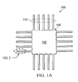
- FIGS. 1A-9 present perspective, plan and cross-sectional views of an example device package 100 at selected stages of manufacture.
- FIG. 1A presents a plan view of an example lead frame 105 which is provided as part of the method.
- the lead frame 105 has a plurality of leads 110.
- One of ordinary skill in the art would be familiar with the processes to manufacture a variety of lead frames types. For instance, one skilled in the art would be familiar with techniques (e.g., photolithography) to define a design layout 115 ( FIG. 1B ) on a metal sheet 120 (e.g., copper or aluminum), and, how to remove parts of the metal sheet 120 outside of the design layout 115 (e.g., stamping or etching) to form the lead frame 105 and leads 110 ( FIG. 1A ).
- techniques e.g., photolithography
- the lead frame 105 can be configured as a quad flat pack (QFP) type lead frame.
- QFP quad flat pack
- other configurations of the lead frame 110 include fusion qual type lead frames, lead frames appropriate for plastic dual in-line integrated circuit packages (PDIP), small outline integrated circuits (SOICs), thin QFPs (TQFPs), low profile QFPs (LPQFPs), small shrink outline plastic packages (SSOP), thin SSOPs (TSSOPs), thin very small-outline packages (TVSOPs), or, other types of lead-containing lead frame packages.
- PDIP plastic dual in-line integrated circuit packages
- SOICs small outline integrated circuits
- TQFPs thin QFPs
- LPQFPs low profile QFPs
- SSOP small shrink outline plastic packages
- TSSOPs thin SSOPs
- TVSOPs thin very small-outline packages
- FIG. 2 presents a higher magnification plan view (corresponding the structure shown within region 2 in FIG. 1 ) to shows the detailed features for one of the plurality of leads 110 of the example lead frame 105 in FIG. 1 .
- FIG. 3 presents a perspective view corresponding to the plan view of FIG. 2 , e.g., along view line A-A, in FIG. 3 .
- a cross-section view along view line B-B would be substantially the same as the plan view shown in FIG. 2 .
- the leads 110 may be asymmetrically dimensioned along these two view lines.
- FIGS. 2 and 3 show the package 100 after forming a notch 205 in at least one of the plurality of leads 110.
- the notch 205 includes at least at least one reentrant angle 210 of greater than 180 degrees.
- the notch 205 is located distal to a pre-defined separation region 215 of the lead 110.
- the notch 205 can be formed as part of the process to manufacture the lead frames 105.
- the notch can be included in the design layout 115 formed on the metal sheet 120 and then formed as part of removing parts of the metal sheet outside of the design layout 115 ( FIG. 1B ).
- a lead frame 105, prefabricated with notch-less leads 110 is further processed to form the notch 205 in the at least one lead 110.
- one or more of the leads 110 can be subject to mechanical or laser cutting, similar to that used to cut the metal sheet 120, to form the notch 205.
- reentrant angle 210 refers to as an interior angle on an outer surface 220 of the lead 110 where the apex 225 of the angle 210 faces into the interior of the lead 110.
- pre-defined separation region 215 refers to that portion of the lead 110 that is designed to be cut in order to isolate the lead 110 from other parts of the lead frame 105 (e.g., mounting portion 125, FIG. 1A ).
- a notch 205 in each one of the leads 110.
- a notch-less lead adjacent to one or more notched leads, could have reduced whisker formation.
- the high electric field associated with the notches in the notched leads could cause reduced metal plating in the pre-defined separation region 215 of an adjacent notch-less lead.
- the notch 205 to circumscribe lateral dimensions (e.g., a thickness 310 and width 315) of the lead 110 which are perpendicular to a long dimension 320 of the lead 110. That is, the notch 205 goes all the way around the lead 110, thereby providing a high electric field strength that is uniform all the way around the notch 205 of the lead 110 when a bias voltage is applied to the lead frame 105.
- the notch 205 can be formed in both the thickness and width dimensions 310, 315.
- the notch 205 can be in the cylindrical dimension perpendicular (not shown) to the long dimension 320 of the lead 110.
- forming the notch 205 on only one side or two sides of the lead 110 can still help to deter whisker formation.
- forming notches 205 in the thickness dimension 310 and covering the width dimension 315 with a mask can deter metal plating in the pre-defined separation region 215, and hence reduce the chances of whisker formation.
- the high electric field associated with the notch 205 may draw a sufficient amount of current to the notch 205 so as to reduce metal plating in the pre-defined separation region 215, even though the notch 205 is only present on one side of the lead 110.
- Additionally such configuration can be advantageous when having the notch 205 circumscribe the lateral dimensions 310, 315 would mechanically weaken the lead 110 to an excessive degree.
- forming the notch 205 includes forming an opening 230 in the lead 110.
- the opening 230 protrudes inward relative to an outer surface 220 of the lead 110.
- the notch can be formed so as to protrude outward.
- FIG. 4A presents a plan view analogous to that shown in FIG. 2 , showing an example embodiment of a notch 205 formed by the method where the notch 205 has a step 410 that protrudes outward from the outer surface 235 of the lead 110.
- the rectangular-shaped step 410 has two reentrant angles 210 in the plane of the lead 110 that is depicted in FIG. 4A .
- FIG. 4B-4C show plan views analogous to the view shown in FIG. 2 , of other example notch shapes.
- the notch 205 can include a wedge-shaped opening 230, here shown with a single reentrant angle 210.
- the notch 205 can include an opening 230 and a step 410, e.g., on different sides of the lead 110.
- additional reentrant angles 210 can be formed by having one or more secondary-openings 420 within the opening 230 or within the step 410 of the notch 205. Based on the present disclosure one skilled in the art would understand how the notch could be formed with a variety of opening or step shapes and combinations thereof.
- the method can further include masking portions of the lead frame in preparation for electroplating.
- FIG. 5 presents a perspective view analogous to that shown in FIG. 3 , showing the lead frame 105 after being placed between first and second plating mask layers 510, 515.
- a semi-transparent view of the mask layers 510, 515 is presented so that underlying structures of the lead frame 105 are visible.
- the mask layers 510, 515 are composed of a rigid insulating material such as a hard plastic or rubber.
- a proximal edge 520 (e.g., the edge proximal to the center of the lead frame 105) of the notch 205 is preferably adjacent to an outer edge 525 of at least one of the, and more preferably both, edges 525, 527, of the plating mask layers 510, 515.
- a mismatching distance 530 between the proximal edge 520 and the edges 525, 527, of the plating mask layers 510, 515 is less than about 10 percent of a total length 535 of the notch 205.
- a distal edge 540 of the notch 205 is not covered by the plating mask layers 510, 515.
- FIG. 6 showing the lead frame 105 of FIG. 5 after electro-depositing a metal plate 610 (e.g., silver plating) on portions the lead 110 not covered by the first and second plating mask layers 510, 515.
- a metal plate 610 e.g., silver plating
- electro-depositing the metal plate 610 includes placing the lead frame 105 and plating mask layers 510, 515 in a metal plating solution and applying a voltage bias to the lead frame 105.
- the lead frame 105 and mask layers 510, 515 are placed in a metal plating solution containing silver cations, and a negative voltage of about -0.9 Volts or greater is applied to the lead frame 105 until the desired thickness 625 of metal plating 610 is obtained.
- the voltage bias applied to the lead frame 105 is in a range of about -1 to -25 Volts.
- metal plate formation is driven by the strength of the electric field on the lead's surface. Due to the presence of the reentrant angle or angles 210 ( FIG. 2 ) the electric field in the vicinity of the notch 205 will be higher than on other regions of the lead 110. Therefore, a relatively larger amount of electric current goes to the notch 205 as compared to other portions of the lead 110. This, in turn, will tends to draw more metal ions to the notch 205, and thereby prevent, or at least reduce, metal ions from plating in a proximal region 630 of the lead 110 (relative to the central portion of the lead frame 105) covered by the plating mask layer 510, 515.
- a first thickness 620 of the metal plate 610 located directly over the notch 205 is greater than a second thickness 625 of the metal plate 610 located over a terminal portion 640 of the lead 110 that is distal to the notch 205.
- this is in contrast to a lead frame having only notch-less leads, where some metal ions can be electro-plated under the mask layers 510, 515 ( FIG. 5 ) and in the pre-defined separation region 215.
- FIG. 7 shows a lower magnification plan view of the lead frame 105 of the package 100 analogous to that shown FIG. 1A , after performing the method steps described in the context of FIGS. 2-6 , and after removing the lead frame 105 from between the mask layer 510, 515, following the deposition of the metal plate 610.
- FIG. 7 illustrates an embodiment in which a plurality of leads 110 were treated according to the method steps described in the context of FIGS. 2-6 .
- the notches 205 ( FIG. 2 ) of the leads 110 are covered by the metal plating 610, and, due to the presence of the notch 205, the metal plating 610 is distal to the pre-defined separation region 215.
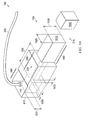
- FIG. 8 show the package 100 of FIG. 7 , after attaching an electronic device 810 to the device mounting portion 125 of the lead frame 105 as part of the package's 100 manufacture.
- the electronic device 810 comprising one or more integrated circuits can be bonded to the mounting portion 125 using an adhesive glue.
- FIG. 8 further shows the package 100 after bonding a wire 830 (e.g., gold wire) from a landing pad 840 of the electronic device 810 to the portion of lead 110 covered with the metal plate 610.
- the wire 830 facilitates the electrical interconnection of the electronic device 810 to other devices (not shown) of, or external to, the package 100.
- a plurality of wire bonds are formed between the landing pads 840 and leads 110, but for clarity, only a few connections are depicted.
- FIG. 8 also shows the package 100 after covering the electronic device 810 and the mounting portion 125 of the lead frame 105 with an insulating mold 850.
- a fluid mold 850 e.g., organic resin or a ceramic material
- the mold 850 can protect the device 810 from exposure damaging environments and can mechanically stabilize the various components of the package 100.
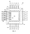
- FIG. 9 shows the package 100 of FIG. 8 after severing the leads 110 from the device mounting portion 125 of the lead frame 105 by cutting within the pre-defined separation regions 215 of the leads 110. Severing can be accomplished by mechanical sawing, laser cutting or other procedures well know to those skilled in the art. Similar procedures may be performed simultaneous, or in separate steps, to sever other portions of the lead frame 105, such as handling bars or other support structures (now shown).
- FIG. 10 shows a perspective detailed view, analogous to the views shown in FIGS. 3 , 5 , and 6 , of an example package 100 of the disclosure.
- the same reference numbers are used to label features that common to the embodiments of FIGS. 1-9 .
- the metal plate 610 is depicted as semi-transparent, and, the mold 950 ( FIG. 9 ) is not depicted.
- FIG. 10 shows the example package 100 after performing the steps described in the context of FIGS. 1-9 .
- the package 100 may comprise the lead frame 105 prior to any one, or all, of the method steps described in the context of FIGS. 5-9 .
- the electronic device package 100 comprises a lead frame 105 having at least one lead 110 with a notch 205 that includes at least one reentrant angle 210 ( FIG. 2 ) of greater than 180 degrees.
- the notch 205 is located distal to a cut end 1010 of the lead 110, e.g., an end 1010 of the lead 110 severed from other portions 1020 of the lead frame 105 such as described in the context of FIG. 9 (e.g., the mounting portion 125, FIG. 8 ).
- each of a plurality of leads 110 of the lead frame 105 includes the notch 205 ( FIG. 2 ).
- the notch 205 circumscribes lateral dimensions 310, 315 of the lead 110, the lateral dimensions 310, 315 being perpendicular to a long dimension 320 of the lead ( FIG. 3 ).
- the notch 205 can include a rectangular-shaped opening 230 in a outer surface 220 of the lead 110 and have at least two reentrant angles 210 ( FIG. 2 ).
- the notch 205 can include a wedge-shaped opening, a step structure 410 that protrudes outward from the surface 220, or combinations thereof, and, the notch 205 can have one or more reentrant angles 210 ( FIGS. 4A-C ). Based on the present disclosure, one skilled in the art would appreciate the variety of other shapes that the notch 205 could have in order to promote having a high electric field strength in the notch region, as discussed elsewhere herein.
- the dimensions of the notch 205 reflect a balance between several factors.
- the notch's size should be sufficiently large to promote a high electric field strength in the vicinity of the notch 205. However the notch's size should be small enough to leave the lead 110 with sufficient mechanical strength to undergo the manufacturing steps and end-use handling without breaking. For instance, too large an opening 230 could render the lead 110 too fragile to handle during the package's manufacture or end-use.
- the notch's size should be sufficiently large to be conducive to controlling the notch's manufacture so that the same-sized notch is reproducibly formed among the leads of a single package, or between packages.
- the notch has an opening with a depth into the lead which does not exceed about 25 percent of a total lateral dimension of the notch-less portions of the lead.
- the depth 1020 of the notch's 205 opening 230 in the width dimension 310 preferably does not exceed about 25 percent of the lead's total width 1025.
- the depth 1030 of the notch's opening 230 in the thickness dimension 315 also does not exceed about 25 percent of the lead's total thickness 1035. Consequently, for notches 205 that circumscribe the lateral dimensions 310, 315 (e.g. FIG.
- the depth 1020, 1030 of the opening 230 ranges from about 5 to 25 percent, and more preferably about 10 to 15 percent, of the total lateral dimensions 310 315 (e.g., the total width 1025 and total thickness 1035) of the lead 110.
- a lead 110 that has a total width 1025 and total thickness 1035 that are each about 0.4 mm in notch-less portions of the lead 110.
- the depth of the opening 230 e.g., width depth 1020 and thickness depth 1030
- the lead 110 can have a smaller opening 230 (e.g., depth of the 1020, 1030 of about 0.01 mm) to preserve the lead's strength.
- the opening 230 it is also advantageous for the opening 230 to be long so as to avoid the electric field from bridge across the notch 205 and thereby reduce the strength of the field in the vicinity of the notch 205. It is also desirable however for the opening's length 535 not to be so long as to cause the lead 110 lose stability or to not having a high field throughout the entire length of the notch 205.
- the opening 230 has a length 535 equal to about 1.5 to 2.5 times the depth 1020, 1030 of the opening 230. For example consider again a lead 110 wherein the total width 1025 and thickness 1035 that are each about 0.4 mm. If the depth 1020, 1030 of the notch's opening 230 was about 0.04 mm, then the length 535 of the opening preferably ranges from about 0.06 mm to 0.08 mm.
- a terminal portion 640 of the lead 110 that is distal to the notch 205 and the notch 205 itself are preferably both covered with a metal plate 610.
- the 110 lead comprises, or in some cases, consists essentially of, copper (e.g., 99 wt% copper or more) and the metal plate 610 comprises, or in some cases, consists essentially of, silver (e.g., 99 wt% or more silver).
- a first thickness 620 the metal plate 610 located directly over the notch 205 is greater (e.g., from about 10 to 100 percent greater) than a second thickness 625 of the metal plate 610 located directly over the terminal portion 630 of the lead 110 ( FIG. 6 ).
- the first thickness 620 can be about 55 to 100 microns.
- the package 100 can further include an electronic device 810 mounted to a mounting portion 125 of the lead frame 110.
- the mounting portion 125 is separated from the lead 110 or (leads 110).
- a portion of the lead proximal 640 to the mounting portion is substantially free of metal plating (e.g., the first thickness 620 the metal plate 610 is less than about 1 micron).
- the package 100 can also include wires 830 bonded from landing pads 840 of the electronic device and to a metal plate 125 covered portion of the lead 110 (e.g., the notch 205, the terminal portion 630 or both).
- the package 100 can also include an insulating mold 850 covering the electronic device 810 and the mounting portion 125 of the lead frame 110.
Landscapes
- Lead Frames For Integrated Circuits (AREA)
- Led Device Packages (AREA)
- Physics & Mathematics (AREA)
- Geometry (AREA)
Applications Claiming Priority (1)
| Application Number | Priority Date | Filing Date | Title |
|---|---|---|---|
| US12/486,592 US8334467B2 (en) | 2009-06-17 | 2009-06-17 | Lead frame design to improve reliability |
Publications (3)
| Publication Number | Publication Date |
|---|---|
| EP2284886A2 true EP2284886A2 (de) | 2011-02-16 |
| EP2284886A3 EP2284886A3 (de) | 2013-02-27 |
| EP2284886B1 EP2284886B1 (de) | 2019-05-15 |
Family
ID=42751498
Family Applications (1)
| Application Number | Title | Priority Date | Filing Date |
|---|---|---|---|
| EP10165969.6A Not-in-force EP2284886B1 (de) | 2009-06-17 | 2010-06-15 | Leiterrahmenentwurf zur Verbesserung der Zuverlässigkeit |
Country Status (6)
| Country | Link |
|---|---|
| US (2) | US8334467B2 (de) |
| EP (1) | EP2284886B1 (de) |
| JP (1) | JP2011003903A (de) |
| KR (1) | KR101676038B1 (de) |
| CN (1) | CN101930935B (de) |
| TW (1) | TWI411082B (de) |
Cited By (1)
| Publication number | Priority date | Publication date | Assignee | Title |
|---|---|---|---|---|
| EP3086367A1 (de) * | 2015-04-20 | 2016-10-26 | Nxp B.V. | Leiterrahmen |
Families Citing this family (6)
| Publication number | Priority date | Publication date | Assignee | Title |
|---|---|---|---|---|
| US8334467B2 (en) | 2009-06-17 | 2012-12-18 | Lsi Corporation | Lead frame design to improve reliability |
| US9693488B2 (en) | 2015-02-13 | 2017-06-27 | Deere & Company | Electronic assembly with one or more heat sinks |
| US9860987B2 (en) | 2015-02-13 | 2018-01-02 | Deere & Company | Electronic assembly with one or more heat sinks |
| CN105698889A (zh) * | 2016-01-27 | 2016-06-22 | 湖南威铭能源科技有限公司 | 湿式光电直读水表表头的通讯线保护结构及其制作工艺 |
| EP3422405B1 (de) * | 2017-01-22 | 2024-12-18 | Shenzhen Goodix Technology Co., Ltd. | Gehäuse für fingerabdruck-sensorchip |
| TWI712129B (zh) | 2020-01-21 | 2020-12-01 | 強茂股份有限公司 | 半導體封裝結構以及其製作方法 |
Family Cites Families (36)
| Publication number | Priority date | Publication date | Assignee | Title |
|---|---|---|---|---|
| JPS5519000Y2 (de) * | 1974-09-13 | 1980-05-06 | ||
| JPS6097654A (ja) * | 1983-11-01 | 1985-05-31 | Toshiba Corp | 封止型半導体装置 |
| JPS61214545A (ja) * | 1985-03-20 | 1986-09-24 | Toshiba Corp | 半導体装置 |
| JPS6254945A (ja) * | 1985-09-04 | 1987-03-10 | Sumitomo Electric Ind Ltd | Ic用リ−ドフレ−ム |
| JPS62169457A (ja) * | 1986-01-22 | 1987-07-25 | Hitachi Micro Comput Eng Ltd | 半導体装置用リ−ドフレ−ム |
| JPS62202546A (ja) * | 1986-02-28 | 1987-09-07 | Shinko Electric Ind Co Ltd | リ−ドフレ−ム |
| JPS6324648A (ja) * | 1986-07-16 | 1988-02-02 | Nec Corp | 半導体装置 |
| JPS63213954A (ja) * | 1987-03-02 | 1988-09-06 | Nec Corp | 樹脂封止部品 |
| JPH0273659A (ja) * | 1988-09-08 | 1990-03-13 | Nec Corp | 半導体装置用のリードフレーム |
| JP2944721B2 (ja) * | 1990-08-22 | 1999-09-06 | 生化学工業株式会社 | エンドトキシンの測定剤 |
| KR930006868A (ko) * | 1991-09-11 | 1993-04-22 | 문정환 | 반도체 패키지 |
| JPH06104361A (ja) * | 1991-10-09 | 1994-04-15 | Hitachi Ltd | 半導体装置およびその製造方法並びにそれに使用されるリードフレーム |
| JPH05183087A (ja) * | 1991-12-28 | 1993-07-23 | Shinko Electric Ind Co Ltd | リードフレーム及びそのめっき方法 |
| JP2745933B2 (ja) * | 1992-02-17 | 1998-04-28 | 日本電気株式会社 | Tab−集積回路 |
| JPH06324648A (ja) | 1993-05-14 | 1994-11-25 | Matsushita Electric Ind Co Ltd | 単純マトリクス型液晶駆動装置と画像データ記憶方法 |
| JP3082518B2 (ja) * | 1993-07-13 | 2000-08-28 | セイコーエプソン株式会社 | 半導体用リードフレーム及び半導体装置 |
| JPH0758267A (ja) * | 1993-08-18 | 1995-03-03 | Toppan Printing Co Ltd | リードフレーム |
| JP3870301B2 (ja) * | 1996-06-11 | 2007-01-17 | ヤマハ株式会社 | 半導体装置の組立法、半導体装置及び半導体装置の連続組立システム |
| US6069406A (en) * | 1997-05-20 | 2000-05-30 | Shinko Electric Industries Co., Ltd. | Wiring patterned film and production thereof |
| US7332375B1 (en) * | 1998-06-24 | 2008-02-19 | Amkor Technology, Inc. | Method of making an integrated circuit package |
| JP2000188366A (ja) * | 1998-12-24 | 2000-07-04 | Hitachi Ltd | 半導体装置 |
| JP3062192B1 (ja) * | 1999-09-01 | 2000-07-10 | 松下電子工業株式会社 | リ―ドフレ―ムとそれを用いた樹脂封止型半導体装置の製造方法 |
| JP4523138B2 (ja) * | 2000-10-06 | 2010-08-11 | ローム株式会社 | 半導体装置およびそれに用いるリードフレーム |
| US6707135B2 (en) * | 2000-11-28 | 2004-03-16 | Texas Instruments Incorporated | Semiconductor leadframe for staggered board attach |
| JP3436254B2 (ja) | 2001-03-01 | 2003-08-11 | 松下電器産業株式会社 | リードフレームおよびその製造方法 |
| SG109495A1 (en) * | 2002-04-16 | 2005-03-30 | Micron Technology Inc | Semiconductor packages with leadfame grid arrays and components and methods for making the same |
| US6812552B2 (en) * | 2002-04-29 | 2004-11-02 | Advanced Interconnect Technologies Limited | Partially patterned lead frames and methods of making and using the same in semiconductor packaging |
| US6777265B2 (en) * | 2002-04-29 | 2004-08-17 | Advanced Interconnect Technologies Limited | Partially patterned lead frames and methods of making and using the same in semiconductor packaging |
| US6797540B1 (en) * | 2002-11-18 | 2004-09-28 | National Semiconductor Corporation | Dap isolation process |
| JP3952963B2 (ja) * | 2003-02-21 | 2007-08-01 | ヤマハ株式会社 | 半導体装置及びその製造方法 |
| US7005728B1 (en) * | 2004-06-03 | 2006-02-28 | National Semiconductor Corporation | Lead configuration for inline packages |
| KR100584699B1 (ko) * | 2004-11-04 | 2006-05-30 | 삼성전자주식회사 | 고정 테이프를 갖는 리드 프레임 |
| JP2006179760A (ja) * | 2004-12-24 | 2006-07-06 | Yamaha Corp | 半導体パッケージ、および、これに使用するリードフレーム |
| US7875988B2 (en) * | 2007-07-31 | 2011-01-25 | Seiko Epson Corporation | Substrate and manufacturing method of the same, and semiconductor device and manufacturing method of the same |
| US7714419B2 (en) * | 2007-12-27 | 2010-05-11 | Stats Chippac Ltd. | Integrated circuit package system with shielding |
| US8334467B2 (en) | 2009-06-17 | 2012-12-18 | Lsi Corporation | Lead frame design to improve reliability |
-
2009
- 2009-06-17 US US12/486,592 patent/US8334467B2/en active Active
-
2010
- 2010-06-10 CN CN201010202799.4A patent/CN101930935B/zh active Active
- 2010-06-10 TW TW099118954A patent/TWI411082B/zh active
- 2010-06-14 KR KR1020100055837A patent/KR101676038B1/ko active Active
- 2010-06-15 EP EP10165969.6A patent/EP2284886B1/de not_active Not-in-force
- 2010-06-17 JP JP2010137977A patent/JP2011003903A/ja not_active Ceased
-
2012
- 2012-11-15 US US13/677,547 patent/US8869389B2/en active Active
Non-Patent Citations (1)
| Title |
|---|
| None |
Cited By (2)
| Publication number | Priority date | Publication date | Assignee | Title |
|---|---|---|---|---|
| EP3086367A1 (de) * | 2015-04-20 | 2016-10-26 | Nxp B.V. | Leiterrahmen |
| US9786585B2 (en) | 2015-04-20 | 2017-10-10 | Nxp B.V. | Lead-frame |
Also Published As
| Publication number | Publication date |
|---|---|
| TWI411082B (zh) | 2013-10-01 |
| CN101930935A (zh) | 2010-12-29 |
| US20130067743A1 (en) | 2013-03-21 |
| EP2284886B1 (de) | 2019-05-15 |
| TW201110296A (en) | 2011-03-16 |
| US8869389B2 (en) | 2014-10-28 |
| CN101930935B (zh) | 2014-07-23 |
| US8334467B2 (en) | 2012-12-18 |
| EP2284886A3 (de) | 2013-02-27 |
| KR20100135659A (ko) | 2010-12-27 |
| JP2011003903A (ja) | 2011-01-06 |
| US20100319987A1 (en) | 2010-12-23 |
| KR101676038B1 (ko) | 2016-11-14 |
Similar Documents
| Publication | Publication Date | Title |
|---|---|---|
| US8869389B2 (en) | Method of manufacturing an electronic device package | |
| US5969411A (en) | Lead frame with increased strength and manufacture of semiconductor device | |
| US7264997B2 (en) | Semiconductor device including inclined cut surface and manufacturing method thereof | |
| CN205609512U (zh) | 半导体封装体 | |
| US11251110B2 (en) | Semiconductor device and method of manufacturing the semiconductor device | |
| US20160100490A1 (en) | Making a plurality of integrated circuit packages | |
| US10707154B2 (en) | Semiconductor device and method for manufacturing the same | |
| JP2022120854A (ja) | 半導体装置用基板および半導体装置 | |
| US12444667B2 (en) | Semiconductor device and method for manufacturing semiconductor device | |
| CN104681449A (zh) | 带有光学检查特征的无引线半导体封装 | |
| JP2015185619A (ja) | 半導体装置用基板、当該基板の製造方法、半導体装置、及び半導体装置の製造方法 | |
| CN101834148B (zh) | 半导体装置及其制造方法 | |
| CN104183507A (zh) | 制造半导体器件的方法 | |
| KR100914051B1 (ko) | 반도체 패키지 제조용 세라믹 기판 | |
| CN207868194U (zh) | 电子部件封装 | |
| JP2000036621A (ja) | 側面型電子部品の電極構造 | |
| EP4447094B1 (de) | Verfahren zur herstellung von halbleiterbauelementen und zugehöriges halbleiterbauelement | |
| EP4576205A1 (de) | Verfahren und vorrichtung zur defektfreien herstellung von halbleiter-chip-verpackungen | |
| TWI900363B (zh) | 無引腳半導體封裝元件的製造方法 | |
| JP7542677B2 (ja) | 半導体装置用基板および半導体装置 | |
| JP4569048B2 (ja) | 面実装型半導体パッケージおよびその製造方法 | |
| TW202504015A (zh) | 具有可潤濕側翼之半導體封裝及相關方法 | |
| JP2026055591A (ja) | 半導体装置の製造方法および半導体装置 | |
| CN118866715A (zh) | 制造半导体设备的方法 | |
| CN119852185A (zh) | 制造半导体器件的方法和对应的半导体器件 |
Legal Events
| Date | Code | Title | Description |
|---|---|---|---|
| PUAI | Public reference made under article 153(3) epc to a published international application that has entered the european phase |
Free format text: ORIGINAL CODE: 0009012 |
|
| AK | Designated contracting states |
Kind code of ref document: A2 Designated state(s): AL AT BE BG CH CY CZ DE DK EE ES FI FR GB GR HR HU IE IS IT LI LT LU LV MC MK MT NL NO PL PT RO SE SI SK SM TR |
|
| AX | Request for extension of the european patent |
Extension state: BA ME RS |
|
| PUAL | Search report despatched |
Free format text: ORIGINAL CODE: 0009013 |
|
| AK | Designated contracting states |
Kind code of ref document: A3 Designated state(s): AL AT BE BG CH CY CZ DE DK EE ES FI FR GB GR HR HU IE IS IT LI LT LU LV MC MK MT NL NO PL PT RO SE SI SK SM TR |
|
| AX | Request for extension of the european patent |
Extension state: BA ME RS |
|
| RIC1 | Information provided on ipc code assigned before grant |
Ipc: H01L 23/495 20060101AFI20130121BHEP |
|
| 17P | Request for examination filed |
Effective date: 20130827 |
|
| RBV | Designated contracting states (corrected) |
Designated state(s): AL AT BE BG CH CY CZ DE DK EE ES FI FR GB GR HR HU IE IS IT LI LT LU LV MC MK MT NL NO PL PT RO SE SI SK SM TR |
|
| 17Q | First examination report despatched |
Effective date: 20140626 |
|
| STAA | Information on the status of an ep patent application or granted ep patent |
Free format text: STATUS: EXAMINATION IS IN PROGRESS |
|
| GRAP | Despatch of communication of intention to grant a patent |
Free format text: ORIGINAL CODE: EPIDOSNIGR1 |
|
| STAA | Information on the status of an ep patent application or granted ep patent |
Free format text: STATUS: GRANT OF PATENT IS INTENDED |
|
| INTG | Intention to grant announced |
Effective date: 20190108 |
|
| GRAS | Grant fee paid |
Free format text: ORIGINAL CODE: EPIDOSNIGR3 |
|
| GRAA | (expected) grant |
Free format text: ORIGINAL CODE: 0009210 |
|
| STAA | Information on the status of an ep patent application or granted ep patent |
Free format text: STATUS: THE PATENT HAS BEEN GRANTED |
|
| AK | Designated contracting states |
Kind code of ref document: B1 Designated state(s): AL AT BE BG CH CY CZ DE DK EE ES FI FR GB GR HR HU IE IS IT LI LT LU LV MC MK MT NL NO PL PT RO SE SI SK SM TR |
|
| REG | Reference to a national code |
Ref country code: CH Ref legal event code: EP Ref country code: GB Ref legal event code: FG4D |
|
| REG | Reference to a national code |
Ref country code: DE Ref legal event code: R096 Ref document number: 602010058875 Country of ref document: DE |
|
| REG | Reference to a national code |
Ref country code: IE Ref legal event code: FG4D |
|
| REG | Reference to a national code |
Ref country code: NL Ref legal event code: FP |
|
| REG | Reference to a national code |
Ref country code: LT Ref legal event code: MG4D |
|
| PG25 | Lapsed in a contracting state [announced via postgrant information from national office to epo] |
Ref country code: NO Free format text: LAPSE BECAUSE OF FAILURE TO SUBMIT A TRANSLATION OF THE DESCRIPTION OR TO PAY THE FEE WITHIN THE PRESCRIBED TIME-LIMIT Effective date: 20190815 Ref country code: FI Free format text: LAPSE BECAUSE OF FAILURE TO SUBMIT A TRANSLATION OF THE DESCRIPTION OR TO PAY THE FEE WITHIN THE PRESCRIBED TIME-LIMIT Effective date: 20190515 Ref country code: HR Free format text: LAPSE BECAUSE OF FAILURE TO SUBMIT A TRANSLATION OF THE DESCRIPTION OR TO PAY THE FEE WITHIN THE PRESCRIBED TIME-LIMIT Effective date: 20190515 Ref country code: AL Free format text: LAPSE BECAUSE OF FAILURE TO SUBMIT A TRANSLATION OF THE DESCRIPTION OR TO PAY THE FEE WITHIN THE PRESCRIBED TIME-LIMIT Effective date: 20190515 Ref country code: SE Free format text: LAPSE BECAUSE OF FAILURE TO SUBMIT A TRANSLATION OF THE DESCRIPTION OR TO PAY THE FEE WITHIN THE PRESCRIBED TIME-LIMIT Effective date: 20190515 Ref country code: PT Free format text: LAPSE BECAUSE OF FAILURE TO SUBMIT A TRANSLATION OF THE DESCRIPTION OR TO PAY THE FEE WITHIN THE PRESCRIBED TIME-LIMIT Effective date: 20190915 Ref country code: ES Free format text: LAPSE BECAUSE OF FAILURE TO SUBMIT A TRANSLATION OF THE DESCRIPTION OR TO PAY THE FEE WITHIN THE PRESCRIBED TIME-LIMIT Effective date: 20190515 Ref country code: LT Free format text: LAPSE BECAUSE OF FAILURE TO SUBMIT A TRANSLATION OF THE DESCRIPTION OR TO PAY THE FEE WITHIN THE PRESCRIBED TIME-LIMIT Effective date: 20190515 |
|
| PG25 | Lapsed in a contracting state [announced via postgrant information from national office to epo] |
Ref country code: BG Free format text: LAPSE BECAUSE OF FAILURE TO SUBMIT A TRANSLATION OF THE DESCRIPTION OR TO PAY THE FEE WITHIN THE PRESCRIBED TIME-LIMIT Effective date: 20190815 Ref country code: LV Free format text: LAPSE BECAUSE OF FAILURE TO SUBMIT A TRANSLATION OF THE DESCRIPTION OR TO PAY THE FEE WITHIN THE PRESCRIBED TIME-LIMIT Effective date: 20190515 Ref country code: GR Free format text: LAPSE BECAUSE OF FAILURE TO SUBMIT A TRANSLATION OF THE DESCRIPTION OR TO PAY THE FEE WITHIN THE PRESCRIBED TIME-LIMIT Effective date: 20190816 |
|
| PG25 | Lapsed in a contracting state [announced via postgrant information from national office to epo] |
Ref country code: SK Free format text: LAPSE BECAUSE OF FAILURE TO SUBMIT A TRANSLATION OF THE DESCRIPTION OR TO PAY THE FEE WITHIN THE PRESCRIBED TIME-LIMIT Effective date: 20190515 Ref country code: RO Free format text: LAPSE BECAUSE OF FAILURE TO SUBMIT A TRANSLATION OF THE DESCRIPTION OR TO PAY THE FEE WITHIN THE PRESCRIBED TIME-LIMIT Effective date: 20190515 Ref country code: EE Free format text: LAPSE BECAUSE OF FAILURE TO SUBMIT A TRANSLATION OF THE DESCRIPTION OR TO PAY THE FEE WITHIN THE PRESCRIBED TIME-LIMIT Effective date: 20190515 Ref country code: DK Free format text: LAPSE BECAUSE OF FAILURE TO SUBMIT A TRANSLATION OF THE DESCRIPTION OR TO PAY THE FEE WITHIN THE PRESCRIBED TIME-LIMIT Effective date: 20190515 Ref country code: CZ Free format text: LAPSE BECAUSE OF FAILURE TO SUBMIT A TRANSLATION OF THE DESCRIPTION OR TO PAY THE FEE WITHIN THE PRESCRIBED TIME-LIMIT Effective date: 20190515 |
|
| REG | Reference to a national code |
Ref country code: CH Ref legal event code: PL |
|
| REG | Reference to a national code |
Ref country code: DE Ref legal event code: R097 Ref document number: 602010058875 Country of ref document: DE |
|
| PG25 | Lapsed in a contracting state [announced via postgrant information from national office to epo] |
Ref country code: IT Free format text: LAPSE BECAUSE OF FAILURE TO SUBMIT A TRANSLATION OF THE DESCRIPTION OR TO PAY THE FEE WITHIN THE PRESCRIBED TIME-LIMIT Effective date: 20190515 Ref country code: SM Free format text: LAPSE BECAUSE OF FAILURE TO SUBMIT A TRANSLATION OF THE DESCRIPTION OR TO PAY THE FEE WITHIN THE PRESCRIBED TIME-LIMIT Effective date: 20190515 Ref country code: MC Free format text: LAPSE BECAUSE OF FAILURE TO SUBMIT A TRANSLATION OF THE DESCRIPTION OR TO PAY THE FEE WITHIN THE PRESCRIBED TIME-LIMIT Effective date: 20190515 |
|
| PLBE | No opposition filed within time limit |
Free format text: ORIGINAL CODE: 0009261 |
|
| STAA | Information on the status of an ep patent application or granted ep patent |
Free format text: STATUS: NO OPPOSITION FILED WITHIN TIME LIMIT |
|
| REG | Reference to a national code |
Ref country code: BE Ref legal event code: MM Effective date: 20190630 |
|
| PG25 | Lapsed in a contracting state [announced via postgrant information from national office to epo] |
Ref country code: TR Free format text: LAPSE BECAUSE OF FAILURE TO SUBMIT A TRANSLATION OF THE DESCRIPTION OR TO PAY THE FEE WITHIN THE PRESCRIBED TIME-LIMIT Effective date: 20190515 |
|
| 26N | No opposition filed |
Effective date: 20200218 |
|
| PG25 | Lapsed in a contracting state [announced via postgrant information from national office to epo] |
Ref country code: IE Free format text: LAPSE BECAUSE OF NON-PAYMENT OF DUE FEES Effective date: 20190615 Ref country code: PL Free format text: LAPSE BECAUSE OF FAILURE TO SUBMIT A TRANSLATION OF THE DESCRIPTION OR TO PAY THE FEE WITHIN THE PRESCRIBED TIME-LIMIT Effective date: 20190515 |
|
| PG25 | Lapsed in a contracting state [announced via postgrant information from national office to epo] |
Ref country code: LI Free format text: LAPSE BECAUSE OF NON-PAYMENT OF DUE FEES Effective date: 20190630 Ref country code: SI Free format text: LAPSE BECAUSE OF FAILURE TO SUBMIT A TRANSLATION OF THE DESCRIPTION OR TO PAY THE FEE WITHIN THE PRESCRIBED TIME-LIMIT Effective date: 20190515 Ref country code: CH Free format text: LAPSE BECAUSE OF NON-PAYMENT OF DUE FEES Effective date: 20190630 Ref country code: LU Free format text: LAPSE BECAUSE OF NON-PAYMENT OF DUE FEES Effective date: 20190615 Ref country code: BE Free format text: LAPSE BECAUSE OF NON-PAYMENT OF DUE FEES Effective date: 20190630 |
|
| PG25 | Lapsed in a contracting state [announced via postgrant information from national office to epo] |
Ref country code: CY Free format text: LAPSE BECAUSE OF FAILURE TO SUBMIT A TRANSLATION OF THE DESCRIPTION OR TO PAY THE FEE WITHIN THE PRESCRIBED TIME-LIMIT Effective date: 20190515 |
|
| PG25 | Lapsed in a contracting state [announced via postgrant information from national office to epo] |
Ref country code: IS Free format text: LAPSE BECAUSE OF FAILURE TO SUBMIT A TRANSLATION OF THE DESCRIPTION OR TO PAY THE FEE WITHIN THE PRESCRIBED TIME-LIMIT Effective date: 20190915 |
|
| PG25 | Lapsed in a contracting state [announced via postgrant information from national office to epo] |
Ref country code: HU Free format text: LAPSE BECAUSE OF FAILURE TO SUBMIT A TRANSLATION OF THE DESCRIPTION OR TO PAY THE FEE WITHIN THE PRESCRIBED TIME-LIMIT; INVALID AB INITIO Effective date: 20100615 Ref country code: MT Free format text: LAPSE BECAUSE OF FAILURE TO SUBMIT A TRANSLATION OF THE DESCRIPTION OR TO PAY THE FEE WITHIN THE PRESCRIBED TIME-LIMIT Effective date: 20190515 |
|
| PG25 | Lapsed in a contracting state [announced via postgrant information from national office to epo] |
Ref country code: MK Free format text: LAPSE BECAUSE OF FAILURE TO SUBMIT A TRANSLATION OF THE DESCRIPTION OR TO PAY THE FEE WITHIN THE PRESCRIBED TIME-LIMIT Effective date: 20190515 |
|
| REG | Reference to a national code |
Ref country code: AT Ref legal event code: UEP Ref document number: 1134426 Country of ref document: AT Kind code of ref document: T Effective date: 20190515 |
|
| P01 | Opt-out of the competence of the unified patent court (upc) registered |
Effective date: 20230521 |
|
| PGFP | Annual fee paid to national office [announced via postgrant information from national office to epo] |
Ref country code: NL Payment date: 20240521 Year of fee payment: 15 |
|
| PGFP | Annual fee paid to national office [announced via postgrant information from national office to epo] |
Ref country code: GB Payment date: 20240521 Year of fee payment: 15 |
|
| PGFP | Annual fee paid to national office [announced via postgrant information from national office to epo] |
Ref country code: DE Payment date: 20240521 Year of fee payment: 15 |
|
| PGFP | Annual fee paid to national office [announced via postgrant information from national office to epo] |
Ref country code: AT Payment date: 20240523 Year of fee payment: 15 |
|
| PGFP | Annual fee paid to national office [announced via postgrant information from national office to epo] |
Ref country code: FR Payment date: 20240522 Year of fee payment: 15 |
|
| REG | Reference to a national code |
Ref country code: DE Ref legal event code: R079 Ref document number: 602010058875 Country of ref document: DE Free format text: PREVIOUS MAIN CLASS: H01L0023495000 Ipc: H10W0070400000 |
|
| REG | Reference to a national code |
Ref country code: DE Ref legal event code: R119 Ref document number: 602010058875 Country of ref document: DE |
|
| REG | Reference to a national code |
Ref country code: NL Ref legal event code: MM Effective date: 20250701 |
|
| REG | Reference to a national code |
Ref country code: AT Ref legal event code: MM01 Ref document number: 1134426 Country of ref document: AT Kind code of ref document: T Effective date: 20250615 |
|
| GBPC | Gb: european patent ceased through non-payment of renewal fee |
Effective date: 20250615 |
|
| PG25 | Lapsed in a contracting state [announced via postgrant information from national office to epo] |
Ref country code: NL Free format text: LAPSE BECAUSE OF NON-PAYMENT OF DUE FEES Effective date: 20250701 |
|
| PG25 | Lapsed in a contracting state [announced via postgrant information from national office to epo] |
Ref country code: GB Free format text: LAPSE BECAUSE OF NON-PAYMENT OF DUE FEES Effective date: 20250615 |
|
| PG25 | Lapsed in a contracting state [announced via postgrant information from national office to epo] |
Ref country code: DE Free format text: LAPSE BECAUSE OF NON-PAYMENT OF DUE FEES Effective date: 20260101 |
|
| PG25 | Lapsed in a contracting state [announced via postgrant information from national office to epo] |
Ref country code: AT Free format text: LAPSE BECAUSE OF NON-PAYMENT OF DUE FEES Effective date: 20250615 |
|
| PG25 | Lapsed in a contracting state [announced via postgrant information from national office to epo] |
Ref country code: FR Free format text: LAPSE BECAUSE OF NON-PAYMENT OF DUE FEES Effective date: 20250630 |