EP2309642A2 - Circuit de polarisation - Google Patents
Circuit de polarisation Download PDFInfo
- Publication number
- EP2309642A2 EP2309642A2 EP10186639A EP10186639A EP2309642A2 EP 2309642 A2 EP2309642 A2 EP 2309642A2 EP 10186639 A EP10186639 A EP 10186639A EP 10186639 A EP10186639 A EP 10186639A EP 2309642 A2 EP2309642 A2 EP 2309642A2
- Authority
- EP
- European Patent Office
- Prior art keywords
- parallel
- inductor
- inductors
- capacitor
- bias circuit
- Prior art date
- Legal status (The legal status is an assumption and is not a legal conclusion. Google has not performed a legal analysis and makes no representation as to the accuracy of the status listed.)
- Granted
Links
Images



Classifications
-
- H—ELECTRICITY
- H03—ELECTRONIC CIRCUITRY
- H03F—AMPLIFIERS
- H03F1/00—Details of amplifiers with only discharge tubes, only semiconductor devices or only unspecified devices as amplifying elements
- H03F1/30—Modifications of amplifiers to reduce influence of variations of temperature or supply voltage or other physical parameters
- H03F1/306—Modifications of amplifiers to reduce influence of variations of temperature or supply voltage or other physical parameters in junction-FET amplifiers
-
- H—ELECTRICITY
- H03—ELECTRONIC CIRCUITRY
- H03F—AMPLIFIERS
- H03F3/00—Amplifiers with only discharge tubes or only semiconductor devices as amplifying elements
- H03F3/189—High-frequency amplifiers, e.g. radio frequency amplifiers
- H03F3/19—High-frequency amplifiers, e.g. radio frequency amplifiers with semiconductor devices only
- H03F3/193—High-frequency amplifiers, e.g. radio frequency amplifiers with semiconductor devices only with field-effect devices
- H03F3/1935—High-frequency amplifiers, e.g. radio frequency amplifiers with semiconductor devices only with field-effect devices with junction-FET devices
-
- H—ELECTRICITY
- H03—ELECTRONIC CIRCUITRY
- H03F—AMPLIFIERS
- H03F2200/00—Indexing scheme relating to amplifiers
- H03F2200/111—Indexing scheme relating to amplifiers the amplifier being a dual or triple band amplifier, e.g. 900 and 1800 MHz, e.g. switched or not switched, simultaneously or not
-
- H—ELECTRICITY
- H03—ELECTRONIC CIRCUITRY
- H03F—AMPLIFIERS
- H03F2200/00—Indexing scheme relating to amplifiers
- H03F2200/18—Indexing scheme relating to amplifiers the bias of the gate of a FET being controlled by a control signal
-
- H—ELECTRICITY
- H03—ELECTRONIC CIRCUITRY
- H03F—AMPLIFIERS
- H03F2200/00—Indexing scheme relating to amplifiers
- H03F2200/451—Indexing scheme relating to amplifiers the amplifier being a radio frequency amplifier
-
- H—ELECTRICITY
- H03—ELECTRONIC CIRCUITRY
- H03F—AMPLIFIERS
- H03F2200/00—Indexing scheme relating to amplifiers
- H03F2200/75—Indexing scheme relating to amplifiers the amplifier stage being a common source configuration MOSFET
Definitions
- the present invention relates to a bias circuit used in an amplifier or the like.
- An active device such as transistors requires a direct-current (DC) power for operation.
- a bias circuit is used to supply the DC power to the active device while isolating transmission paths of an alternating-current (AC) signal from a DC power supply.
- AC alternating-current
- an amplification device outputs the amplified AC signal at an output terminal.
- the main energy of the amplified signal comes from the DC power supply. That is, the amplifier converts the energy received from the DC power supply to that of the AC signal.
- the bias circuit serves to pass the energy from the DC power supply to the amplification device. In order not to affect the transmission of the AC signal, the bias circuit has a filtering function for preventing the AC signal from flowing into the bias circuit.
- Fig. 1 shows an exemplary configuration of a conventional bias circuit 900 that supplies a DC voltage to an active device (FET) 180.
- a bias supply terminal 800 of the bias circuit 900 is connected to a line between an AC signal source 1 and the active device 180 (between a port A and a port B).
- the bias circuit 900 includes a parallel resonant circuit 78p with a capacitor 7 having a capacitance C 1 and an inductor 8 having an inductance L 1 connected in parallel with each other.
- One end of the parallel resonant circuit 78p corresponds to the bias supply terminal 800 and the other end of the parallel resonant circuit 78p corresponds to a terminal 600 where a DC circuit part 10 with a DC circuit 5, such as a choke coil, and a DC power supply 6 is connected.
- the DC power supply 6 generates a certain DC voltage with respect to the ground potential.
- a capacitor 4 having a sufficiently-large capacitance and grounded at one end thereof is connected to the terminal 600.
- the energy of the DC power supply 6 is supplied to the active device 180 via the terminal 600 and the bias supply terminal 800.
- the resonance frequency of the parallel resonant circuit 78p denoted by a character f is determined by the capacitance C 1 and the inductance L 1 .
- the impedance of the bias circuit 900 as viewed from the bias supply terminal 800 toward the DC power supply 6 is considered infinite, so that no AC signal enters the bias circuit.
- the bias circuit 900 is a bias circuit that operates at the resonance frequency f.
- the filtering function of the resonant circuit of the conventional bias circuit 900 or the like is effective only in the proximity of the resonant frequency.
- the amplifier is an essential component of the RF circuits. That is, the amplifier also is desired to operate in multiple bands.
- Several methods for enabling multiband operation of the amplifier have been proposed.
- One example is an amplifier capable of simultaneously amplifying signals in two inherent frequency bands (see “Dual-band Power SiMOSFET Amplifier with Two-section Impedance Transformers", Uchida et al., 2004 IEICE General Conference, C-2-39, referred to as Non-Patent literature 1 hereinafter).
- the multi-band amplifier can be applied to a system capable of high-speed transmission using a plurality of frequency bands, such as spectrum aggregation.
- the bias circuit itself has to operate in multiple bands.
- the conventional bias circuit 900 is difficult to apply to the multiband amplifier.
- the multi-band amplifier disclosed in Non-Patent literature 1 has a bias circuit that comprises a parallel resonant circuit and a transmission line Q having an effect similar to that of the parallel resonant circuit connected in series with each other.
- This bias circuit is designed in such a manner that the resonance frequency of the parallel resonant circuit is a first frequency and the transmission line Q is a quarter-wave line that is short-circuited at the tip at a second frequency. Therefore, this bias circuit can supply energy of a DC power supply to the multiband amplifier simultaneously at two different frequency bands.
- bias circuit capable of multiband operation is a bias circuit disclosed in Japanese Patent Application Laid-Open No. 2006-254378 .
- This bias circuit supplies energy of a DC power supply separately for a plurality of frequency bands by switching and cannot supply energy from a DC power supply simultaneously for a plurality of frequency bands.
- an object of the present invention is to provide a bias circuit that has high design flexibility and can supply a DC voltage and/or a direct current to an active device simultaneously for a plurality of frequency bands.
- the bias circuit comprises: a bias supply terminal for supplying a DC voltage and/or a direct current to an active device; a capacitor (a parallel capacitor) connected at one end thereof to the bias supply terminal and grounded at the other end thereof; and a parallel circuit connected in parallel with the parallel capacitor and connected at one end thereof to the bias supply terminal.
- N denote a predetermined integer equal to or greater than 2
- q denote each integer equal to or greater than 2 and equal to or smaller than N-1
- m denote each integer equal to or greater than 1 and equal to or smaller than N-1.
- the parallel circuit comprises: a DC power supply connection terminal connected to a DC circuit part including a DC power supply; N inductors (parallel inductors) connected in series with each other; and N-1 series resonators, wherein a first parallel inductor of the N parallel inductors is connected at one end thereof to the bias supply terminal, a q-th parallel inductor of the N parallel inductors is connected at one end thereof to the other end of a (q-1)-th parallel inductor of the N parallel inductors and connected at the other end thereof to one end of a (q+1)-th parallel inductor of the N parallel inductors, an N-th parallel inductor of the N parallel inductors is connected at the other end thereof to the DC power supply connection terminal, and an m-th series resonator of the N-1 series resonators includes an m-th capacitor (a resonant capacitor) and an m-th inductor (a resonant inductor) and is connected at one end thereof to a
- a series resonator in a bias circuit has an impedance of zero at the resonance frequency of the series resonator.
- a short circuit state (a short-circuited state from the viewpoint of an AC signal) occurs at a connecting point (between parallel inductors) to which the series resonator is connected.
- the bias circuit is effectively equivalent to an arrangement comprising a parallel capacitor, and one or more parallel inductors and one or more series resonators that exist between the short-circuited connecting point and a bias supply terminal. This holds true for each of the series resonators in the bias circuit.
- the reactance of each component in the bias circuit is appropriately set so that the impedance of the bias circuit as viewed from the bias supply terminal toward the bias circuit is infinite (that is, the admittance is zero) at each resonance frequency, a DC voltage and/or a direct current can be supplied to an active device simultaneously for a plurality of frequency bands without a switching operation or the like.
- the impedance of the series resonator to a direct current is infinite, no direct current flows through the series resonator.
- the bias circuit is easy to design.
- the bias circuit can have a smaller size.
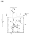
- Fig. 2 shows a bias circuit 100 according to an embodiment of the present invention that can supply a DC voltage and/or a direct current from a DC power supply 6 to an active device 180 simultaneously for two different frequency bands f 1 and f 2 .
- the bias circuit 100 is used on the input terminal side of an amplifier.
- a bias supply terminal 800 of the bias circuit 100 is connected to a line between an AC signal source 1 and an active device 180 (between a port A and a port B).
- the active device 180 may be a transistor, a field effect transistor (FET), a metal oxide semiconductor FET (MOSFET), a thin film transistor (TFT), or the like.
- FET field effect transistor
- MOSFET metal oxide semiconductor FET
- TFT thin film transistor
- the active device 180 shown in the drawings is an n-channel junction FET, the n-channel junction FET is only an example of the active device 180, and the present invention is not limited to the n-channel junction FET.
- the bias circuit 100 includes: a capacitor 3 having a capacitance C p , grounded at one end thereof and connected at the other end thereof to the bias supply terminal 800 (referred to as a parallel capacitor hereinafter); and a parallel circuit 3R connected in parallel with the parallel capacitor 3 and connected at one end thereof to the bias supply terminal 800.
- the parallel circuit 3R includes: an inductor 2 1 having an inductance L p1 and connected at one end thereof to the bias supply terminal 800 (referred to as a first parallel inductor hereinafter); an inductor 2 2 having an inductance L p2 and connected at one end thereof to the other end of the first parallel inductor 2 1 and connected at the other end thereof to a DC power supply connection terminal 600 (referred to as a second parallel inductor hereinafter); a first series resonator 9 1 connected at one end thereof to a connecting point 700 1 between the first parallel inductor 2 1 and the second parallel inductor 2 2 ; a capacitor 4 having a capacitance C and connected at one end thereof to the DC power supply connection terminal 600 and grounded at the other end thereof (referred to as a grounding capacitor hereinafter); and a DC circuit part 10 connected to the DC power supply connection terminal 600.
- the first series resonator 9 1 includes: a capacitor 7 1 having a capacitance C s1 and connected at one end thereof to the connecting point 700 1 (referred to as a first resonant capacitor hereinafter); and an inductor 8 1 having an inductance L s1 and connected at one end thereof to the other end of the capacitor 7 1 and grounded at the other end thereof (referred to as a first resonant inductor hereinafter).
- the DC circuit part 10 includes: a DC circuit 5, such as a choke coil, connected at one end thereof to the DC power supply connection terminal 600; and a DC power supply 6 that is connected to the other end of the DC circuit 5 and generates a certain DC voltage with respect to the ground potential. The energy from the DC power supply 6 is supplied to the active device 180 via the bias supply terminal 800.
- the grounding capacitor 4 has a sufficiently-large capacitance C, and the impedance of the grounding capacitor 4 is substantially zero (a short circuit state) in any desired frequency bands.
- a resonance frequency of the first series resonator 9 1 is referred to as a first frequency f 1 .
- the first frequency f 1 , an inductance L s1 and the capacitance C s1 are related according to the following formula (1).
- f 1 1 2 ⁇ ⁇ ⁇ L s ⁇ 1 ⁇ C s ⁇ 1
- the impedance of the first series resonator 9 1 as viewed from the connecting point 700 1 toward the first series resonator 9 1 is zero (a short circuit state).
- the short circuit state always occurs at the connecting point 700 1 regardless of what circuit is connected between the connecting point 700 1 and the DC power supply connection terminal 600. Therefore, at the first frequency f 1 , the impedance of the bias circuit 100 as viewed from the bias supply terminal 800 toward the bias circuit 100 is determined by the parallel capacitor 3 and the first parallel inductor 2 1 .
- a combined admittance Y p1 of the parallel capacitor 3 and the first parallel inductor 2 1 is expressed by the following formula (2).
- Y p ⁇ 1 j ⁇ ⁇ 1 ⁇ C p + 1 j ⁇ ⁇ 1 ⁇ L p ⁇ 1
- the inductance L p1 of the first parallel inductor 2 1 associated with the capacitance C p of the parallel capacitor 3 is determined so that the combined admittance Y p1 is zero.
- L p ⁇ 1 1 2 ⁇ ⁇ ⁇ f 1 2 ⁇ C p
- the impedance of the bias circuit 100 as viewed from the bias supply terminal 800 toward the bias circuit 100 is infinite, so that the bias circuit 100 has no effect on the signal at the first frequency f 1 .
- the short circuit state does not occur at the connecting point 700 1 , and the inductance Lp 2 of the second parallel inductor is set so that a combined impedance of the parallel capacitor 3, the first parallel inductor 2 1 , the first series resonator 9 1 and the second parallel inductor 2 2 is infinite.
- a combined admittance Y p2 of the bias circuit 100 (in this case, a combined admittance of the parallel capacitor 3, the first parallel inductor 2 1 , the first series resonator 9 1 and the second parallel inductor 2 2 ) at the second frequency f 2 can be expressed by the following approximate formula (4).
- the inductance L p2 of the second parallel inductor 2 2 is determined according to the following formula (5) so that the combined admittance Y p2 is zero.
- L p ⁇ 2 1 2 ⁇ ⁇ ⁇ f 2 2 ⁇ C p - L p ⁇ 1
- the impedance of the bias circuit 100 as viewed from the bias supply terminal 800 toward the bias circuit 100 is infinite, and thus, the bias circuit 100 have no effect on the signal at the second frequency f 2 . Therefore, the DC voltage and/or the direct current from the DC power supply 6 are simultaneously supplied to the active device 180 without affecting the transmission characteristics of the AC signals at the desired two frequencies f 1 and f 2 .
- the frequencies are preferably related according to f 1 > f 2 .
- Z s12 of the first series resonator 9 1 at the second frequency f 2 is expressed by the following formula (6).
- the impedance Z s12 increases as the capacitance C s1 of the first resonant capacitor 7 1 decreases.
- the inductance L s1 of the first resonant inductor 8 1 has to be increased.
- the inductor is formed by a winding. Therefore, if the inductance is increased while maintaining the allowable current of the wire, the size of the inductor increases, and the parasitic capacitance also increases accordingly, so that the desired inductance may not be able to be achieved in a high frequency band.
- the bias circuit according to the present invention is also expected to handle a high direct current when the bias circuit is applied to a power amplifier.
- the impedance of the first series resonator 9 1 to a DC is infinite as shown by the formula (6), no direct current flows into the first resonant inductor 8 1 . Therefore, an inductor having a low allowable current can be used as a resonant inductor in the first series resonator 9 1 .
- the bias circuit it is not difficult to design the capacitor in the series resonator to have a low capacitance and the inductor in the series resonator to have a high inductance, and as a result, the impedance at frequencies other than the resonance frequency of the series resonator can be designed to be high.
- the bias circuit can be easily designed.
- the inductance L p1 of the first parallel inductor 2 1 and the inductance L p2 of the second parallel inductor 2 2 can be decreased by appropriately setting the capacitance C p of the parallel capacitor 3. More specifically, for the bias circuit according to the present invention, the inductance of each parallel inductor can be easily decreased by increasing the capacitance C p of the parallel capacitor 3. Thus, the bias circuit can be easily designed and reduced in size.
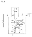
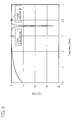
- Fig. 4 shows pass characteristics (S21) of an AC signal from the port A to the port B in the bias circuit shown in Fig. 3 . As can be seen from the drawing, the loss is extremely low at each frequency, and the bias circuit 100 has substantially no effect on the AC signal.
- the bias circuit 100 described above can supply a DC voltage and/or a direct current to an active device simultaneously for two different frequency bands.
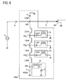
- the bias circuit 200 includes: a parallel capacitor 3 having a capacitance C p and grounded at one end thereof and connected at the other end thereof to a bias supply terminal 800; and a parallel circuit 3L connected in parallel with the parallel capacitor 3 and connected at one end thereof to the bias supply terminal 800.
- the parallel circuit 3L includes: a first parallel inductor 2 1 having an inductance L p(1) connected at one end thereof to the bias supply terminal 800; a q-th parallel inductor 2 q having an inductance L p(q) and connected at one end thereof to the other end of a (q-1)-th parallel inductor 2 q-1 and connected at the other end thereof to one end of a (q+1)-th parallel inductor 2 q+1 where q denotes each integer equal to or greater than 2 and equal to or smaller than N-1; an N-th parallel inductor 2 N having an inductance L p(N) and connected at one end thereof to the other end of an (N-1)-th parallel inductor 2 N-1 and connected at the other end thereof to a DC power supply connection terminal 600; an m-th series resonator 9 m connected at one end thereof to a connecting point 700 m between an m-th parallel inductor 2 m and an (m+1)-th parallel inductor 2
- the m-th series resonator 9 m includes: an m-th resonant capacitor 7 m having a capacitance C sm and connected at one end thereof to the connecting point 700 m ; and an m-th resonant inductor 8 m having an inductance L sm and connected at one end thereof to the other end of the m-th resonant capacitor 7 m and grounded at the other end thereof.
- the DC circuit part 10 includes: a DC circuit 5, such as a choke coil, connected at one end thereof to the DC power supply connection terminal 600; and a DC power supply 6 that is connected to the other end of the DC circuit 5 and generates a certain DC voltage with respect to the ground potential. The energy of the DC power supply 6 is supplied to an active device 180 via the bias supply terminal 800.
- n denotes each integer equal to or greater than 2 and equal to or smaller than N
- a resonance frequency of an (n-1)-th series resonator 9 n-1 is referred to as an (n-1)-th frequency f n-1 .
- the frequency f n-1 , the inductance L s(n-1) , and the capacitance C s(n-1) are related to each other according to the following formula (7).
- f n - 1 1 2 ⁇ ⁇ ⁇ L s ⁇ n - 1 ⁇ C s ⁇ n - 1
- the inductances of the first parallel inductor 2 1 and the second parallel inductor 2 2 can be determined in the same way as for the bias circuit 100 described above.
- n is an integer equal to or greater than 3 or equal to or smaller than N
- the impedance of the (n-1)-th series resonator 9 n-1 as viewed from the connecting point 700 n-1 toward the (n-1)-th series resonator 9 n-1 is zero (a short circuit state) at the (n-1)-th frequency f n-1 .
- the inductance L p(n-1) of the (n-1)-th parallel inductor 2 n-1 is determined so that the impedance of the bias circuit 200 as viewed from the bias supply terminal 800 toward the bias circuit 200 (a combined impedance of the parallel capacitor 3, the first to the (n-1)-th parallel inductors 2 1 to 2 n-1 , and the first to the (n-2)-th series resonators 9 1 to 9 n-2 ) is infinite.
- a combined admittance Y p(n-1) of the bias circuit in this case, a combined admittance of the parallel capacitor 3, the first to the (n-1)-th parallel inductors 2 1 to 2 n-1 , and the first to the (n-2)-th series resonators 9 1 to 9 n-2 ) at the (n-1)-th frequency f n-1 is expressed by the following approximate formula (8).
- the inductance L p(n-1) is determined according to the following formula (9) so that the combined admittance Y p(N-1) is zero.
- L p ⁇ n - 1 1 2 ⁇ ⁇ ⁇ f n - 1 2 ⁇ C p - L p ⁇ 1 + ⁇ + L p ⁇ n - 2
- the combined admittance Y p(n-1) of the parallel capacitor 3 and the first to the (n-1)-th parallel inductors 2 1 to 2 n-1 at the (n-1)-th frequency f n-1 is 0, or in other words, a combined impedance Z p(n-1) of the parallel capacitor 3 and the first to the (n-1)-th parallel inductors 2 1 to 2 n-1 is infinite, the impedance of the bias circuit 200 as viewed from the bias supply terminal 800 toward the bias circuit 200 is infinite, and thus, the bias circuit 200 have no effect on the signal at the (n-1)-th frequency f n-1 .
- the inductance L pN of the N-th parallel inductor 2 N is determined so that the combined impedance of the parallel capacitor 3, the first to N-th parallel inductors 2 1 to 2 N and the first to the (N-1)-the series resonators 9 1 to 9 N-1 is infinite at the N-th frequency f N .
- a combined admittance Y pN of the bias circuit (in this case, a combined admittance of the parallel capacitor 3, the first to N-th parallel inductors 2 1 to 2 N and the first to the (N-1)-th series resonators 9 1 to 9 N-1 ) at the N-th frequency f N is expressed by the following approximate formula (10).
- the inductance L pN of the N-th parallel inductor 2 N is determined according to the following formula (11) so that the combined admittance Y pN is zero.
- L p ⁇ N 1 2 ⁇ ⁇ ⁇ f N 2 ⁇ C p - L p ⁇ 1 + ⁇ + L p ⁇ N - 1
- the impedance of the bias circuit 200 as viewed from the bias supply terminal 800 toward the bias circuit 200 is infinite, and thus, the bias circuit 200 have no effect on the signal at the N-th frequency f N .
- the bias circuit 200 is preferably designed so that f 1 > f 2 > ... > f N-1 > f N .
- the capacitance of each resonant capacitor and the inductance of each resonant inductor are determined so that the impedance of each of the first to the (n-2)-th series resonators 9 1 to 9 n-2 is sufficiently large (the admittance of each of the series resonators 9 1 to 9 n-2 is substantially zero) at the (n-1)-th frequency f n-1
- the impedance of each of the first to the (n-2)-th series resonators 9 1 to 9 n-2 is also sufficiently large (the admittance of each of the series resonators 9 1 to 9 n-2 is substantially zero) at the n-th frequency f n .
- the impedance of a resonant capacitor is inversely proportional to the frequency. Therefore, at the n-th frequency f n , the capacitance of the resonant capacitor of the (n-1)-th series resonator 9 n-1 and the inductance of the resonant inductor of the (n-1)-th series resonator 9 n-1 can be determined so that the impedance of the (n-1)-th series resonator 9 n-1 is sufficiently large (the admittance of the (n-1)-th series resonator 9 n-1 is substantially zero).
- the impedance Z sny increases as a capacitance C sn of an n-th resonant capacitor 7 n decreases.
- the capacitance C sn decreases, an inductance L sn of an n-th resonant inductor 8 n has to be increased.
- the impedance of the n-th series resonator 9 n to a direct current is infinite as described above, no direct current flows into the n-th resonant inductor 8 n .
- an inductor having a low allowable current can be used as a resonant inductor in the n-th series resonator 9 n . That is, in designing the bias circuit capable of simultaneous biasing for N different frequencies according to the present invention, it is not difficult to design the capacitors in the series resonators to have low capacitances and the inductors in the series resonators to have high inductances, and as a result, the impedance at frequencies other than the resonance frequencies of the series resonators can be designed to be high. Thus, the bias circuit can be easily designed.
- the inductance of each of the first to the N-th parallel inductors 2 1 to 2 N can be decreased by appropriately setting the capacitance C p of the parallel capacitor 3. More specifically, for the bias circuit according to the present invention, the inductance of each parallel inductor can be easily decreased by increasing the capacitance C p of the parallel capacitor 3. Thus, the bias circuit can be easily designed and reduced in size.
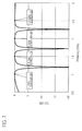
- Fig. 7 shows pass characteristics of an AC signal from a port A to a port B in the bias circuit shown in Fig. 6 . As can be seen from the drawing, the loss is extremely low at each frequency, and the bias circuit 200w has substantially no effect on the AC signal.
- the bias circuit according to the present invention can supply a DC voltage and/or a direct current to an active device simultaneously for AC signals in N different frequency bands, the AC signals in the N frequency bands do not always have to flow between the port A and the port B.
- the bias circuit according to the present invention can supply a DC voltage and/or a direct current even when only AC signals in some of the N frequency bands flow between the port A and the port B.
- the m-th series resonators 9 m are shown as including: the m-th resonant capacitor 7 m having a capacitance C sm and connected at one end thereof to the connecting point 700 m ; and the m-th inductor 8 m having an inductance L sm and connected at one end thereof to the other end of the m-th resonant capacitor 7 m and grounded at the other end thereof.
- the present invention is not limited to such configurations.
- all or some of the N-1 series resonators in the bias circuit 200 may be configured in the same way as a second series resonator 91 2 shown in Fig.
- an m-th resonant inductor 8 m having an inductance L sm and connected at one end thereof to the connecting point 700 m ; and an m-th resonant capacitor 7 m having a capacitance C sm and connected at one end thereof to the other end of the m-th resonant inductor 8 m and grounded at the other end thereof.
Landscapes
- Engineering & Computer Science (AREA)
- Power Engineering (AREA)
- Amplifiers (AREA)
- Filters And Equalizers (AREA)
- Waveguide Connection Structure (AREA)
Applications Claiming Priority (1)
| Application Number | Priority Date | Filing Date | Title |
|---|---|---|---|
| JP2009233570A JP5161856B2 (ja) | 2009-10-07 | 2009-10-07 | バイアス回路 |
Publications (3)
| Publication Number | Publication Date |
|---|---|
| EP2309642A2 true EP2309642A2 (fr) | 2011-04-13 |
| EP2309642A3 EP2309642A3 (fr) | 2011-07-13 |
| EP2309642B1 EP2309642B1 (fr) | 2013-04-17 |
Family
ID=43567687
Family Applications (1)
| Application Number | Title | Priority Date | Filing Date |
|---|---|---|---|
| EP10186639.0A Not-in-force EP2309642B1 (fr) | 2009-10-07 | 2010-10-06 | Circuit de polarisation |
Country Status (5)
| Country | Link |
|---|---|
| US (1) | US8570117B2 (fr) |
| EP (1) | EP2309642B1 (fr) |
| JP (1) | JP5161856B2 (fr) |
| KR (1) | KR101097088B1 (fr) |
| CN (1) | CN102035481B (fr) |
Families Citing this family (4)
| Publication number | Priority date | Publication date | Assignee | Title |
|---|---|---|---|---|
| US8653907B2 (en) * | 2011-07-18 | 2014-02-18 | Raytheon Company | Resonated bypass capacitor for enhanced performance of a microwave circuit |
| JP6168349B2 (ja) * | 2013-06-05 | 2017-07-26 | 株式会社村田製作所 | 電力増幅器および無線通信装置 |
| JP6536525B2 (ja) * | 2016-10-04 | 2019-07-03 | 株式会社村田製作所 | バイアスt回路 |
| WO2022162785A1 (fr) * | 2021-01-27 | 2022-08-04 | 三菱電機株式会社 | Dispositif source de puissance |
Citations (1)
| Publication number | Priority date | Publication date | Assignee | Title |
|---|---|---|---|---|
| JP2006254378A (ja) | 2005-03-14 | 2006-09-21 | Ntt Docomo Inc | バイアス回路 |
Family Cites Families (24)
| Publication number | Priority date | Publication date | Assignee | Title |
|---|---|---|---|---|
| JPH06103810B2 (ja) | 1989-09-13 | 1994-12-14 | 三菱電機株式会社 | 電界効果トランジスタ増幅器 |
| JPH04129308A (ja) * | 1990-09-20 | 1992-04-30 | Fujitsu Ltd | 高周波増幅器 |
| JP3438953B2 (ja) | 1994-07-20 | 2003-08-18 | 三洋電機株式会社 | バイアス回路 |
| JPH0884030A (ja) * | 1994-09-12 | 1996-03-26 | Matsushita Electric Ind Co Ltd | 高周波電力増幅器 |
| JPH08204472A (ja) * | 1995-01-24 | 1996-08-09 | Nec Eng Ltd | 高周波増幅回路 |
| JPH08204487A (ja) * | 1995-01-30 | 1996-08-09 | Oki Electric Ind Co Ltd | 有極形フィルタ |
| JPH09186533A (ja) * | 1995-12-30 | 1997-07-15 | Sony Corp | 伝送装置 |
| JPH09289421A (ja) * | 1996-04-24 | 1997-11-04 | Kyocera Corp | 高周波用電力増幅器 |
| KR100229765B1 (ko) * | 1996-12-28 | 1999-11-15 | 유기범 | Fet를 이용한 고주파증폭기의 단일전원 바이어스회로 |
| US6933780B2 (en) * | 2000-02-03 | 2005-08-23 | Matsushita Electric Industrial Co., Ltd. | Predistortion circuit and power amplifier |
| FR2811827B1 (fr) | 2000-07-12 | 2002-10-11 | St Microelectronics Sa | Dispositif d'amplification a faible bruit, en particulier pour un telephone mobile cellulaire |
| US6326849B1 (en) | 2000-09-28 | 2001-12-04 | Eic Corporation | Isolation circuit for use in RF amplifier bias circuit |
| US7034620B2 (en) | 2002-04-24 | 2006-04-25 | Powerwave Technologies, Inc. | RF power amplifier employing bias circuit topologies for minimization of RF amplifier memory effects |
| JP3717463B2 (ja) | 2002-06-26 | 2005-11-16 | 沖電気工業株式会社 | 移動通信システム及び移動通信装置 |
| JP2005094635A (ja) * | 2003-09-19 | 2005-04-07 | Alps Electric Co Ltd | 電力増幅器のバイアス回路 |
| JP4588699B2 (ja) | 2004-04-28 | 2010-12-01 | 三菱電機株式会社 | バイアス回路 |
| JP4575818B2 (ja) * | 2005-03-24 | 2010-11-04 | Okiセミコンダクタ株式会社 | 増幅回路用バイアス回路 |
| JP4788506B2 (ja) * | 2006-07-14 | 2011-10-05 | 日本電気株式会社 | 増幅器 |
| CN200959590Y (zh) * | 2006-09-11 | 2007-10-10 | 沈锦成 | 功率放大器的偏置电路 |
| JP4841394B2 (ja) * | 2006-10-18 | 2011-12-21 | パナソニック株式会社 | 電力増幅器 |
| JP5143523B2 (ja) * | 2006-10-25 | 2013-02-13 | 株式会社エヌ・ティ・ティ・ドコモ | バイアス回路 |
| US8289103B2 (en) * | 2006-11-20 | 2012-10-16 | Panasonic Corporation | Filter device having attenuation poles |
| JP5086630B2 (ja) | 2006-12-20 | 2012-11-28 | 株式会社エヌ・ティ・ティ・ドコモ | 整合回路、デュアルバンド電力増幅器 |
| JP5079387B2 (ja) | 2007-05-10 | 2012-11-21 | 株式会社エヌ・ティ・ティ・ドコモ | 整合回路 |
-
2009
- 2009-10-07 JP JP2009233570A patent/JP5161856B2/ja not_active Expired - Fee Related
-
2010
- 2010-09-29 CN CN201010299067.1A patent/CN102035481B/zh not_active Expired - Fee Related
- 2010-09-29 KR KR1020100094159A patent/KR101097088B1/ko not_active Expired - Fee Related
- 2010-10-05 US US12/898,164 patent/US8570117B2/en not_active Expired - Fee Related
- 2010-10-06 EP EP10186639.0A patent/EP2309642B1/fr not_active Not-in-force
Patent Citations (1)
| Publication number | Priority date | Publication date | Assignee | Title |
|---|---|---|---|---|
| JP2006254378A (ja) | 2005-03-14 | 2006-09-21 | Ntt Docomo Inc | バイアス回路 |
Non-Patent Citations (1)
| Title |
|---|
| UCHIDA ET AL.: "Dual-band Power SiMOSFET Amplifier with Two-section Impedance Transformers", IEICE GENERAL CONFERENCE, 2004, pages C-2 - 39 |
Also Published As
| Publication number | Publication date |
|---|---|
| US8570117B2 (en) | 2013-10-29 |
| KR101097088B1 (ko) | 2011-12-22 |
| CN102035481B (zh) | 2014-04-16 |
| EP2309642B1 (fr) | 2013-04-17 |
| JP5161856B2 (ja) | 2013-03-13 |
| JP2011082809A (ja) | 2011-04-21 |
| EP2309642A3 (fr) | 2011-07-13 |
| KR20110037862A (ko) | 2011-04-13 |
| CN102035481A (zh) | 2011-04-27 |
| US20110080230A1 (en) | 2011-04-07 |
Similar Documents
| Publication | Publication Date | Title |
|---|---|---|
| US8736378B1 (en) | Reconfigureable output matching network for multi band RF power amplifier | |
| EP2214311B1 (fr) | Correspondance de circuit multi-bande et d'amplificateur de puissance multi-bande | |
| EP2421151A2 (fr) | Circuit d'adaptation d'impédance multi-bande | |
| US20070008034A1 (en) | Two stage microwave Class E power amplifier | |
| JP2010087934A (ja) | 整合回路、高周波電力増幅器および携帯電話機 | |
| US9209760B2 (en) | High-frequency, broadband amplifier circuit | |
| US9973155B2 (en) | Apparatus and methods for tunable power amplifiers | |
| US8437723B2 (en) | Amplifier circuit and communication device | |
| KR102775313B1 (ko) | 고주파 증폭기 | |
| EP2309642B1 (fr) | Circuit de polarisation | |
| US7187231B2 (en) | Apparatus, methods and articles of manufacture for multiband signal processing | |
| CN107634729A (zh) | 一种多倍频程超宽带放大器电路 | |
| EP2903157B1 (fr) | Dispositif amplificateur hyperfréquence | |
| US20110215981A1 (en) | High frequency transmission module with improved harmonic feature | |
| KR100789918B1 (ko) | 광대역 저잡음 증폭기의 입력 매칭 회로 | |
| KR100882131B1 (ko) | 집적형 수동 소자 | |
| EP3016281B1 (fr) | Circuit de polarisation d'amplificateur à semi-conducteurs et dispositif d'amplificateur à semi-conducteurs | |
| US7675366B2 (en) | Integrated amplifier circuit | |
| EP3780390A1 (fr) | Amplificateur distribué | |
| JP2015195449A (ja) | マルチバンド高周波電力増幅器 | |
| JP2015070368A (ja) | 半導体装置 | |
| US12470174B2 (en) | Radiofrequency amplifier | |
| Hwang et al. | Study of the inter-stage capacitor effects of a RF CMOS power amplifier to enhance its efficiency | |
| JP2013131802A (ja) | Rf電力増幅器およびその動作方法 | |
| US9219450B1 (en) | High linearity low noise amplifier |
Legal Events
| Date | Code | Title | Description |
|---|---|---|---|
| PUAI | Public reference made under article 153(3) epc to a published international application that has entered the european phase |
Free format text: ORIGINAL CODE: 0009012 |
|
| 17P | Request for examination filed |
Effective date: 20101006 |
|
| AK | Designated contracting states |
Kind code of ref document: A2 Designated state(s): AL AT BE BG CH CY CZ DE DK EE ES FI FR GB GR HR HU IE IS IT LI LT LU LV MC MK MT NL NO PL PT RO RS SE SI SK SM TR |
|
| AX | Request for extension of the european patent |
Extension state: BA ME |
|
| PUAL | Search report despatched |
Free format text: ORIGINAL CODE: 0009013 |
|
| AK | Designated contracting states |
Kind code of ref document: A3 Designated state(s): AL AT BE BG CH CY CZ DE DK EE ES FI FR GB GR HR HU IE IS IT LI LT LU LV MC MK MT NL NO PL PT RO RS SE SI SK SM TR |
|
| AX | Request for extension of the european patent |
Extension state: BA ME |
|
| 17Q | First examination report despatched |
Effective date: 20120308 |
|
| GRAP | Despatch of communication of intention to grant a patent |
Free format text: ORIGINAL CODE: EPIDOSNIGR1 |
|
| GRAS | Grant fee paid |
Free format text: ORIGINAL CODE: EPIDOSNIGR3 |
|
| GRAA | (expected) grant |
Free format text: ORIGINAL CODE: 0009210 |
|
| AK | Designated contracting states |
Kind code of ref document: B1 Designated state(s): AL AT BE BG CH CY CZ DE DK EE ES FI FR GB GR HR HU IE IS IT LI LT LU LV MC MK MT NL NO PL PT RO RS SE SI SK SM TR |
|
| REG | Reference to a national code |
Ref country code: GB Ref legal event code: FG4D |
|
| REG | Reference to a national code |
Ref country code: CH Ref legal event code: EP |
|
| REG | Reference to a national code |
Ref country code: IE Ref legal event code: FG4D |
|
| REG | Reference to a national code |
Ref country code: AT Ref legal event code: REF Ref document number: 607828 Country of ref document: AT Kind code of ref document: T Effective date: 20130515 |
|
| REG | Reference to a national code |
Ref country code: DE Ref legal event code: R096 Ref document number: 602010006212 Country of ref document: DE Effective date: 20130613 |
|
| REG | Reference to a national code |
Ref country code: AT Ref legal event code: MK05 Ref document number: 607828 Country of ref document: AT Kind code of ref document: T Effective date: 20130417 |
|
| REG | Reference to a national code |
Ref country code: LT Ref legal event code: MG4D |
|
| REG | Reference to a national code |
Ref country code: NL Ref legal event code: VDEP Effective date: 20130417 |
|
| PG25 | Lapsed in a contracting state [announced via postgrant information from national office to epo] |
Ref country code: BE Free format text: LAPSE BECAUSE OF FAILURE TO SUBMIT A TRANSLATION OF THE DESCRIPTION OR TO PAY THE FEE WITHIN THE PRESCRIBED TIME-LIMIT Effective date: 20130417 Ref country code: FI Free format text: LAPSE BECAUSE OF FAILURE TO SUBMIT A TRANSLATION OF THE DESCRIPTION OR TO PAY THE FEE WITHIN THE PRESCRIBED TIME-LIMIT Effective date: 20130417 Ref country code: GR Free format text: LAPSE BECAUSE OF FAILURE TO SUBMIT A TRANSLATION OF THE DESCRIPTION OR TO PAY THE FEE WITHIN THE PRESCRIBED TIME-LIMIT Effective date: 20130718 Ref country code: SE Free format text: LAPSE BECAUSE OF FAILURE TO SUBMIT A TRANSLATION OF THE DESCRIPTION OR TO PAY THE FEE WITHIN THE PRESCRIBED TIME-LIMIT Effective date: 20130417 Ref country code: NO Free format text: LAPSE BECAUSE OF FAILURE TO SUBMIT A TRANSLATION OF THE DESCRIPTION OR TO PAY THE FEE WITHIN THE PRESCRIBED TIME-LIMIT Effective date: 20130717 Ref country code: AT Free format text: LAPSE BECAUSE OF FAILURE TO SUBMIT A TRANSLATION OF THE DESCRIPTION OR TO PAY THE FEE WITHIN THE PRESCRIBED TIME-LIMIT Effective date: 20130417 Ref country code: LT Free format text: LAPSE BECAUSE OF FAILURE TO SUBMIT A TRANSLATION OF THE DESCRIPTION OR TO PAY THE FEE WITHIN THE PRESCRIBED TIME-LIMIT Effective date: 20130417 Ref country code: ES Free format text: LAPSE BECAUSE OF FAILURE TO SUBMIT A TRANSLATION OF THE DESCRIPTION OR TO PAY THE FEE WITHIN THE PRESCRIBED TIME-LIMIT Effective date: 20130728 Ref country code: SI Free format text: LAPSE BECAUSE OF FAILURE TO SUBMIT A TRANSLATION OF THE DESCRIPTION OR TO PAY THE FEE WITHIN THE PRESCRIBED TIME-LIMIT Effective date: 20130417 Ref country code: PT Free format text: LAPSE BECAUSE OF FAILURE TO SUBMIT A TRANSLATION OF THE DESCRIPTION OR TO PAY THE FEE WITHIN THE PRESCRIBED TIME-LIMIT Effective date: 20130819 Ref country code: IS Free format text: LAPSE BECAUSE OF FAILURE TO SUBMIT A TRANSLATION OF THE DESCRIPTION OR TO PAY THE FEE WITHIN THE PRESCRIBED TIME-LIMIT Effective date: 20130817 |
|
| PG25 | Lapsed in a contracting state [announced via postgrant information from national office to epo] |
Ref country code: RS Free format text: LAPSE BECAUSE OF FAILURE TO SUBMIT A TRANSLATION OF THE DESCRIPTION OR TO PAY THE FEE WITHIN THE PRESCRIBED TIME-LIMIT Effective date: 20130417 Ref country code: PL Free format text: LAPSE BECAUSE OF FAILURE TO SUBMIT A TRANSLATION OF THE DESCRIPTION OR TO PAY THE FEE WITHIN THE PRESCRIBED TIME-LIMIT Effective date: 20130417 Ref country code: LV Free format text: LAPSE BECAUSE OF FAILURE TO SUBMIT A TRANSLATION OF THE DESCRIPTION OR TO PAY THE FEE WITHIN THE PRESCRIBED TIME-LIMIT Effective date: 20130417 Ref country code: HR Free format text: LAPSE BECAUSE OF FAILURE TO SUBMIT A TRANSLATION OF THE DESCRIPTION OR TO PAY THE FEE WITHIN THE PRESCRIBED TIME-LIMIT Effective date: 20130417 Ref country code: CY Free format text: LAPSE BECAUSE OF FAILURE TO SUBMIT A TRANSLATION OF THE DESCRIPTION OR TO PAY THE FEE WITHIN THE PRESCRIBED TIME-LIMIT Effective date: 20130417 Ref country code: BG Free format text: LAPSE BECAUSE OF FAILURE TO SUBMIT A TRANSLATION OF THE DESCRIPTION OR TO PAY THE FEE WITHIN THE PRESCRIBED TIME-LIMIT Effective date: 20130717 |
|
| PG25 | Lapsed in a contracting state [announced via postgrant information from national office to epo] |
Ref country code: SK Free format text: LAPSE BECAUSE OF FAILURE TO SUBMIT A TRANSLATION OF THE DESCRIPTION OR TO PAY THE FEE WITHIN THE PRESCRIBED TIME-LIMIT Effective date: 20130417 Ref country code: EE Free format text: LAPSE BECAUSE OF FAILURE TO SUBMIT A TRANSLATION OF THE DESCRIPTION OR TO PAY THE FEE WITHIN THE PRESCRIBED TIME-LIMIT Effective date: 20130417 Ref country code: DK Free format text: LAPSE BECAUSE OF FAILURE TO SUBMIT A TRANSLATION OF THE DESCRIPTION OR TO PAY THE FEE WITHIN THE PRESCRIBED TIME-LIMIT Effective date: 20130417 Ref country code: CZ Free format text: LAPSE BECAUSE OF FAILURE TO SUBMIT A TRANSLATION OF THE DESCRIPTION OR TO PAY THE FEE WITHIN THE PRESCRIBED TIME-LIMIT Effective date: 20130417 |
|
| PLBE | No opposition filed within time limit |
Free format text: ORIGINAL CODE: 0009261 |
|
| STAA | Information on the status of an ep patent application or granted ep patent |
Free format text: STATUS: NO OPPOSITION FILED WITHIN TIME LIMIT |
|
| PG25 | Lapsed in a contracting state [announced via postgrant information from national office to epo] |
Ref country code: IT Free format text: LAPSE BECAUSE OF FAILURE TO SUBMIT A TRANSLATION OF THE DESCRIPTION OR TO PAY THE FEE WITHIN THE PRESCRIBED TIME-LIMIT Effective date: 20130417 Ref country code: NL Free format text: LAPSE BECAUSE OF FAILURE TO SUBMIT A TRANSLATION OF THE DESCRIPTION OR TO PAY THE FEE WITHIN THE PRESCRIBED TIME-LIMIT Effective date: 20130417 Ref country code: RO Free format text: LAPSE BECAUSE OF FAILURE TO SUBMIT A TRANSLATION OF THE DESCRIPTION OR TO PAY THE FEE WITHIN THE PRESCRIBED TIME-LIMIT Effective date: 20130417 |
|
| 26N | No opposition filed |
Effective date: 20140120 |
|
| REG | Reference to a national code |
Ref country code: DE Ref legal event code: R097 Ref document number: 602010006212 Country of ref document: DE Effective date: 20140120 |
|
| PG25 | Lapsed in a contracting state [announced via postgrant information from national office to epo] |
Ref country code: MC Free format text: LAPSE BECAUSE OF FAILURE TO SUBMIT A TRANSLATION OF THE DESCRIPTION OR TO PAY THE FEE WITHIN THE PRESCRIBED TIME-LIMIT Effective date: 20130417 |
|
| REG | Reference to a national code |
Ref country code: IE Ref legal event code: MM4A |
|
| REG | Reference to a national code |
Ref country code: FR Ref legal event code: ST Effective date: 20140630 |
|
| PG25 | Lapsed in a contracting state [announced via postgrant information from national office to epo] |
Ref country code: FR Free format text: LAPSE BECAUSE OF NON-PAYMENT OF DUE FEES Effective date: 20131031 |
|
| PG25 | Lapsed in a contracting state [announced via postgrant information from national office to epo] |
Ref country code: IE Free format text: LAPSE BECAUSE OF NON-PAYMENT OF DUE FEES Effective date: 20131006 |
|
| PG25 | Lapsed in a contracting state [announced via postgrant information from national office to epo] |
Ref country code: SM Free format text: LAPSE BECAUSE OF FAILURE TO SUBMIT A TRANSLATION OF THE DESCRIPTION OR TO PAY THE FEE WITHIN THE PRESCRIBED TIME-LIMIT Effective date: 20130417 |
|
| REG | Reference to a national code |
Ref country code: CH Ref legal event code: PL |
|
| PG25 | Lapsed in a contracting state [announced via postgrant information from national office to epo] |
Ref country code: TR Free format text: LAPSE BECAUSE OF FAILURE TO SUBMIT A TRANSLATION OF THE DESCRIPTION OR TO PAY THE FEE WITHIN THE PRESCRIBED TIME-LIMIT Effective date: 20130417 |
|
| PG25 | Lapsed in a contracting state [announced via postgrant information from national office to epo] |
Ref country code: MK Free format text: LAPSE BECAUSE OF FAILURE TO SUBMIT A TRANSLATION OF THE DESCRIPTION OR TO PAY THE FEE WITHIN THE PRESCRIBED TIME-LIMIT Effective date: 20130417 Ref country code: LU Free format text: LAPSE BECAUSE OF NON-PAYMENT OF DUE FEES Effective date: 20131006 Ref country code: LI Free format text: LAPSE BECAUSE OF NON-PAYMENT OF DUE FEES Effective date: 20141031 Ref country code: CH Free format text: LAPSE BECAUSE OF NON-PAYMENT OF DUE FEES Effective date: 20141031 Ref country code: HU Free format text: LAPSE BECAUSE OF FAILURE TO SUBMIT A TRANSLATION OF THE DESCRIPTION OR TO PAY THE FEE WITHIN THE PRESCRIBED TIME-LIMIT; INVALID AB INITIO Effective date: 20101006 |
|
| PG25 | Lapsed in a contracting state [announced via postgrant information from national office to epo] |
Ref country code: MT Free format text: LAPSE BECAUSE OF FAILURE TO SUBMIT A TRANSLATION OF THE DESCRIPTION OR TO PAY THE FEE WITHIN THE PRESCRIBED TIME-LIMIT Effective date: 20130417 |
|
| PG25 | Lapsed in a contracting state [announced via postgrant information from national office to epo] |
Ref country code: AL Free format text: LAPSE BECAUSE OF FAILURE TO SUBMIT A TRANSLATION OF THE DESCRIPTION OR TO PAY THE FEE WITHIN THE PRESCRIBED TIME-LIMIT Effective date: 20130417 |
|
| PGFP | Annual fee paid to national office [announced via postgrant information from national office to epo] |
Ref country code: DE Payment date: 20180925 Year of fee payment: 9 |
|
| PGFP | Annual fee paid to national office [announced via postgrant information from national office to epo] |
Ref country code: GB Payment date: 20181003 Year of fee payment: 9 |
|
| REG | Reference to a national code |
Ref country code: DE Ref legal event code: R119 Ref document number: 602010006212 Country of ref document: DE |
|
| PG25 | Lapsed in a contracting state [announced via postgrant information from national office to epo] |
Ref country code: DE Free format text: LAPSE BECAUSE OF NON-PAYMENT OF DUE FEES Effective date: 20200501 |
|
| GBPC | Gb: european patent ceased through non-payment of renewal fee |
Effective date: 20191006 |
|
| PG25 | Lapsed in a contracting state [announced via postgrant information from national office to epo] |
Ref country code: GB Free format text: LAPSE BECAUSE OF NON-PAYMENT OF DUE FEES Effective date: 20191006 |