EP2472577B1 - Substrat de dispositif électronique et dispositif électronique - Google Patents
Substrat de dispositif électronique et dispositif électronique Download PDFInfo
- Publication number
- EP2472577B1 EP2472577B1 EP11275161.5A EP11275161A EP2472577B1 EP 2472577 B1 EP2472577 B1 EP 2472577B1 EP 11275161 A EP11275161 A EP 11275161A EP 2472577 B1 EP2472577 B1 EP 2472577B1
- Authority
- EP
- European Patent Office
- Prior art keywords
- substrate
- electrode
- light
- layer
- columnar heat
- Prior art date
- Legal status (The legal status is an assumption and is not a legal conclusion. Google has not performed a legal analysis and makes no representation as to the accuracy of the status listed.)
- Not-in-force
Links
Images











Classifications
-
- H—ELECTRICITY
- H05—ELECTRIC TECHNIQUES NOT OTHERWISE PROVIDED FOR
- H05K—PRINTED CIRCUITS; CASINGS OR CONSTRUCTIONAL DETAILS OF ELECTRIC APPARATUS; MANUFACTURE OF ASSEMBLAGES OF ELECTRICAL COMPONENTS
- H05K3/00—Apparatus or processes for manufacturing printed circuits
- H05K3/46—Manufacturing multilayer circuits
-
- H—ELECTRICITY
- H10—SEMICONDUCTOR DEVICES; ELECTRIC SOLID-STATE DEVICES NOT OTHERWISE PROVIDED FOR
- H10W—GENERIC PACKAGES, INTERCONNECTIONS, CONNECTORS OR OTHER CONSTRUCTIONAL DETAILS OF DEVICES COVERED BY CLASS H10
- H10W70/00—Package substrates; Interposers; Redistribution layers [RDL]
- H10W70/60—Insulating or insulated package substrates; Interposers; Redistribution layers
- H10W70/62—Insulating or insulated package substrates; Interposers; Redistribution layers characterised by their interconnections
- H10W70/63—Vias, e.g. via plugs
- H10W70/635—Through-vias
-
- H—ELECTRICITY
- H05—ELECTRIC TECHNIQUES NOT OTHERWISE PROVIDED FOR
- H05K—PRINTED CIRCUITS; CASINGS OR CONSTRUCTIONAL DETAILS OF ELECTRIC APPARATUS; MANUFACTURE OF ASSEMBLAGES OF ELECTRICAL COMPONENTS
- H05K1/00—Printed circuits
- H05K1/02—Details
-
- H—ELECTRICITY
- H05—ELECTRIC TECHNIQUES NOT OTHERWISE PROVIDED FOR
- H05K—PRINTED CIRCUITS; CASINGS OR CONSTRUCTIONAL DETAILS OF ELECTRIC APPARATUS; MANUFACTURE OF ASSEMBLAGES OF ELECTRICAL COMPONENTS
- H05K3/00—Apparatus or processes for manufacturing printed circuits
- H05K3/40—Forming printed elements for providing electric connections to or between printed circuits
-
- H—ELECTRICITY
- H10—SEMICONDUCTOR DEVICES; ELECTRIC SOLID-STATE DEVICES NOT OTHERWISE PROVIDED FOR
- H10H—INORGANIC LIGHT-EMITTING SEMICONDUCTOR DEVICES HAVING POTENTIAL BARRIERS
- H10H20/00—Individual inorganic light-emitting semiconductor devices having potential barriers, e.g. light-emitting diodes [LED]
- H10H20/80—Constructional details
- H10H20/85—Packages
- H10H20/858—Means for heat extraction or cooling
- H10H20/8582—Means for heat extraction or cooling characterised by their shape
-
- H—ELECTRICITY
- H10—SEMICONDUCTOR DEVICES; ELECTRIC SOLID-STATE DEVICES NOT OTHERWISE PROVIDED FOR
- H10W—GENERIC PACKAGES, INTERCONNECTIONS, CONNECTORS OR OTHER CONSTRUCTIONAL DETAILS OF DEVICES COVERED BY CLASS H10
- H10W40/00—Arrangements for thermal protection or thermal control
- H10W40/20—Arrangements for cooling
- H10W40/22—Arrangements for cooling characterised by their shape, e.g. having conical or cylindrical projections
- H10W40/226—Arrangements for cooling characterised by their shape, e.g. having conical or cylindrical projections characterised by projecting parts, e.g. fins to increase surface area
- H10W40/228—Arrangements for cooling characterised by their shape, e.g. having conical or cylindrical projections characterised by projecting parts, e.g. fins to increase surface area the projecting parts being wire-shaped or pin-shaped
-
- H—ELECTRICITY
- H10—SEMICONDUCTOR DEVICES; ELECTRIC SOLID-STATE DEVICES NOT OTHERWISE PROVIDED FOR
- H10W—GENERIC PACKAGES, INTERCONNECTIONS, CONNECTORS OR OTHER CONSTRUCTIONAL DETAILS OF DEVICES COVERED BY CLASS H10
- H10W70/00—Package substrates; Interposers; Redistribution layers [RDL]
- H10W70/01—Manufacture or treatment
- H10W70/05—Manufacture or treatment of insulating or insulated package substrates, or of interposers, or of redistribution layers
- H10W70/095—Manufacture or treatment of insulating or insulated package substrates, or of interposers, or of redistribution layers of vias therein
-
- H—ELECTRICITY
- H10—SEMICONDUCTOR DEVICES; ELECTRIC SOLID-STATE DEVICES NOT OTHERWISE PROVIDED FOR
- H10W—GENERIC PACKAGES, INTERCONNECTIONS, CONNECTORS OR OTHER CONSTRUCTIONAL DETAILS OF DEVICES COVERED BY CLASS H10
- H10W70/00—Package substrates; Interposers; Redistribution layers [RDL]
- H10W70/60—Insulating or insulated package substrates; Interposers; Redistribution layers
- H10W70/62—Insulating or insulated package substrates; Interposers; Redistribution layers characterised by their interconnections
- H10W70/66—Conductive materials thereof
- H10W70/664—Carbon-based materials, e.g. fullerenes
-
- H—ELECTRICITY
- H10—SEMICONDUCTOR DEVICES; ELECTRIC SOLID-STATE DEVICES NOT OTHERWISE PROVIDED FOR
- H10H—INORGANIC LIGHT-EMITTING SEMICONDUCTOR DEVICES HAVING POTENTIAL BARRIERS
- H10H20/00—Individual inorganic light-emitting semiconductor devices having potential barriers, e.g. light-emitting diodes [LED]
- H10H20/01—Manufacture or treatment
- H10H20/036—Manufacture or treatment of packages
- H10H20/0364—Manufacture or treatment of packages of interconnections
-
- H—ELECTRICITY
- H10—SEMICONDUCTOR DEVICES; ELECTRIC SOLID-STATE DEVICES NOT OTHERWISE PROVIDED FOR
- H10H—INORGANIC LIGHT-EMITTING SEMICONDUCTOR DEVICES HAVING POTENTIAL BARRIERS
- H10H20/00—Individual inorganic light-emitting semiconductor devices having potential barriers, e.g. light-emitting diodes [LED]
- H10H20/80—Constructional details
- H10H20/85—Packages
- H10H20/8506—Containers
-
- H—ELECTRICITY
- H10—SEMICONDUCTOR DEVICES; ELECTRIC SOLID-STATE DEVICES NOT OTHERWISE PROVIDED FOR
- H10W—GENERIC PACKAGES, INTERCONNECTIONS, CONNECTORS OR OTHER CONSTRUCTIONAL DETAILS OF DEVICES COVERED BY CLASS H10
- H10W72/00—Interconnections or connectors in packages
- H10W72/50—Bond wires
- H10W72/531—Shapes of wire connectors
- H10W72/5363—Shapes of wire connectors the connected ends being wedge-shaped
-
- H—ELECTRICITY
- H10—SEMICONDUCTOR DEVICES; ELECTRIC SOLID-STATE DEVICES NOT OTHERWISE PROVIDED FOR
- H10W—GENERIC PACKAGES, INTERCONNECTIONS, CONNECTORS OR OTHER CONSTRUCTIONAL DETAILS OF DEVICES COVERED BY CLASS H10
- H10W74/00—Encapsulations, e.g. protective coatings
-
- H—ELECTRICITY
- H10—SEMICONDUCTOR DEVICES; ELECTRIC SOLID-STATE DEVICES NOT OTHERWISE PROVIDED FOR
- H10W—GENERIC PACKAGES, INTERCONNECTIONS, CONNECTORS OR OTHER CONSTRUCTIONAL DETAILS OF DEVICES COVERED BY CLASS H10
- H10W90/00—Package configurations
- H10W90/701—Package configurations characterised by the relative positions of pads or connectors relative to package parts
- H10W90/721—Package configurations characterised by the relative positions of pads or connectors relative to package parts of bump connectors
- H10W90/724—Package configurations characterised by the relative positions of pads or connectors relative to package parts of bump connectors between a chip and a stacked insulating package substrate, interposer or RDL
Definitions
- the present invention relates to a substrate for an electronic device and an electronic device.
- US 2009/083975 discloses related art.
- electronic devices such as various scales of integrated circuits, various types of semiconductor elements and chips thereof, for example, there has been employed a method of disposing an element on a substrate and connecting them by means of wire bonding or the like.
- this method not only requires the process of wire bonding but also increases the mounting area with the number of elements, so that the signal delay increases because of an increase in wiring length.
- TSV through-silicon-via
- Japanese Unexamined Patent Application Publication Nos. 11-298138 , 2000-228410 , 2002-158191 and 2003-257891 disclose a through electrode formation technology essential for the TSV technology.
- the superiority of the TSV technology over the wire bonding is as follows.
- the number of connections is limited to 100 to 200 in the wire bonding, but the use of the TSV technology makes it possible to arrange connecting through electrodes at intervals of the order of ⁇ m, increasing the number of connections to several thousand.
- connection distance can be minimized, it is less likely to be affected by noise; since parasitic capacitance and resistance are low, it is possible to reduce delay, attenuation, or waveform degradation; an additional circuit is not required for amplification or electrostatic breakdown protection; and with these advantages, there can be realized high speed action and low power consumption of the circuit.
- TSV technology makes it possible to obtain not only an electronic device including an analog or digital circuit, a memory circuit such as a DRAM, a logic circuit such as a CPU or the like but also an electronic device including different types of circuits such as an analog high frequency circuit and a low frequency, low power consumption circuit prepared in different processes and stacked together.
- TSV three-dimensional integrated circuit
- a via through electrode
- Cu electroplating a method of forming a through electrode by Cu electroplating.
- the electroplating decreases the production efficiency because of its inevitable long processing time.
- the via typically has an aspect ratio of 5 or more and usually has a rugged inner wall surface, it is difficult to uniformly form a plating primary film over the inner wall surface of the via. This produces a void or gap between the inner wall surface of the via and a plating film to be used as the through electrode, thereby causing an increase in electrical resistance, decreased reliability and so on.
- the electrical resistance cannot be set lower than the inherent electrical resistance of Cu.
- the progress in improving the packaging density, the performance and the processing speed and reducing the size, the thickness and the weight of the electronic device because of the use of the TSV technology not only increases heat that will be generated by the operation but also makes it difficult to prepare a heat dissipation structure for it, so that the question of how to dissipate heat becomes a major issue. If the heat dissipation is insufficient, accumulation of the generated heat leads to abnormal heat generation, impairing bonding strength of the electronic component and damaging reliability of the electrical connection or changing electrical characteristics of the electronic component and at worst, causing thermal runaway, thermal breakdown or the like.
- Japanese Unexamined Patent Application Publication No. 2008-294253 discloses a technology of forming a heat transmission via conductor by filling a conductive paste including Ag powder.
- Japanese Unexamined Patent Application Publication No. 2005-158957 discloses a technology of forming a thermal via, wherein the thermal via comprises a metal (copper, solder or gold) having a good thermal conductivity and a via is formed from an upper surface of a light-emitting element submount structure, the via is coated with gold at its side face and then filled with solder.
- thermo conductor comprising a metal powder-containing resin such as a silver paste or a copper paste, a composite of a metal rod and the metal powder-containing resin or the like.
- a thermal via comprising a metal such as Cu or Ni.
- nm-sized means having a size within a range of 1 ⁇ m or less.
- nanocomposite structure means that at least two kinds of components are combined to constitute a composite where the components are nm-sized particles or in a crystal or amorphous phase.
- the through electrode is a casting formed by using a via formed in the substrate as a mold, as described above, the substrate can be provided with a through electrode that has a high adhesion strength to a side wall surface of the via, a compact structure free from any cavity, void or hollow, a low electrical resistance and an excellent electrical conductivity. Even if the inner wall surface of the via has irregularities, the through electrode can be casted to conform to the irregularities, so that there can be obtained a through electrode having a high adhesion strength to the via.
- the through electrode can be casted to conform to the irregularities of the inner wall surface of the via
- the through electrode and the irregularities of the inner wall surface of the via serve as an anchor for preventing slippage of the through electrode, thereby increasing the bonding strength of the through electrode to the substrate.
- the inner wall surface of the via does not require accuracy for the irregularities, but rather a preferable result can be obtained with certain irregularities. This makes it easy to form the via.
- the through electrodes can be used as a positive or negative electrode for an electronic component or an electronic device to be mounted on the substrate. Therefore, electrical wiring such as wire bonding becomes unnecessary, so that the product cost can be reduced by cutting the production facility cost that has been spent on an expensive wire bonding apparatus.
- the through electrode has a nanocomposite structure including a nm-sized carbon nanotube.
- the carbon nanotube has a high thermal conductivity which is 10 times greater than that of copper. This makes it possible to realize a through electrode having extremely high heat dissipation characteristics.
- the carbon nanotube also has a high current density resistance of 10 9 A/cm 2 which is more than 1,000 times greater than that of copper. Moreover, since the carbon nanotube has less electron scattering as compared with copper being a good electrical conductor, it has a low electrical resistance. As compared with copper, accordingly, the through electrode including a carbon nanotube has a low electrical resistance and can reduce the quantity of heat due to resistance even if a large current is passed.
- the through electrode has a nanocomposite structure including a nm-sized carbon nanotube having such characteristics.
- stress can be reduced because of the nm-sized effect. This inhibits characteristic degradation of a semiconductor circuit in a semiconductor substrate. It can also inhibit the occurrence of fracturing or cracking of the substrate.
- the through electrode has a nanocomposite structure including the nm-sized carbon nanotube and a metal/alloy component having a nanocomposite crystal structure. Since the through electrode having a nanocomposite structure including the nm-sized carbon nanotube and the metal/alloy component having a nanocomposite crystal structure includes a structure (crystal) whose size is limited to a nano level, stress that will be generated in the through electrode can be reduced accordingly. Moreover, the nanocomposite crystal structure is also capable of facilitating formation of equiaxed crystal in the vertical conductor.
- the above-described particular characteristics of the nanocomposite crystal structure and the nanocomposite structure inhibit characteristic degradation of a semiconductor circuit, particularly, in a semiconductor substrate. It can also inhibit the occurrence of fracturing or cracking of the substrate.
- nanocomposite crystal structure basically refers to a structure in which nanoparticles are dispersed in crystal grains (intragranular nanocomposite crystal structure) or a structure in which nanoparticles are dispersed in grain boundaries (interglanular nanocomposite crystal structure).
- It may also comprise a composite material that is turned into a paste by mixing the carbon nanotube with an organic material, wherein, if necessary, inorganic powder may be mixed or a metal/alloy component having a nanocomposite crystal structure may be added as a third component.
- the substrate supporting the through electrode can include at least one of an inorganic substrate such as of ceramic, an organic substrate such as one used for a copper-clad substrate and a semiconductor substrate.
- the through electrode is electrically insulated from the conductive inorganic substrate, the conductive organic substrate and the semiconductor substrate by an electrical insulating film or layer.
- This insulating structure can be realized by an insulating film obtained by oxidizing or nitriding the inner wall surface of a via that will act as a mold for the through electrode or an insulating layer adhered to the inner wall surface of the via.
- the above-described insulating structure may be provided in the form of a ring at a small distance around the via.
- the present invention provides a substrate comprising a plurality of columnar heat sinks independently of or along with the through electrodes.
- the columnar heat sink is a casting formed by using a via formed in the substrate as a mold.
- the columnar heat sink is also a casting formed by using a via formed in the substrate as a mold, the substrate can be provided with a columnar heat sink that has a high adhesion strength to the side wall surface of the via, a compact structure free from any cavity, void or hollow and excellent thermal conductivity and heat dissipation characteristics.
- the columnar heat sink having a high adhesion strength to the side wall surface of the via and a compact structure free from any cavity, void or hollow can be formed efficiently in a short time, as compared with the case where it is formed by using another method such as plating.
- the columnar heat sink has a nanocomposite structure including a metal/alloy component having a nanocomposite crystal structure. This results in reducing stress that will be generated in the columnar heat sink. Moreover, the nanocomposite crystal structure is also capable of facilitating formation of equiaxed crystal in the columnar heat sink.
- the above-described particular characteristics of the nanocomposite crystal structure and the nanocomposite structure inhibit characteristic degradation of a semiconductor circuit formed on a semiconductor substrate (wafer). It can also inhibit the occurrence of fracturing or cracking of the semiconductor substrate.
- the columnar heat sink may include a nm-sized carbon atom structure having an excellent thermal conductivity along with the metal/alloy component having a nanocomposite crystal structure.
- a carbon atom structure includes at least one of a diamond, a fullerene and a carbon nanotube.
- the above-described columnar heat sink has excellent heat dissipation characteristics because of the high thermal conductivity of the carbon atom structure.
- the carbon nanotube has a high thermal conductivity which is 10 times greater than that of copper, ensuring extremely high heat dissipation characteristics. It may comprise a composite material that is turned into a paste by further adding an organic component as a third component, if necessary.
- the substrate according to the present invention may comprise both the through electrode and the columnar heat sink. Specifically, it may be constructed as follows.
- the above-described substrate can be combined with an electronic component to provide an electronic device.
- the electronic component is mounted on the substrate.
- an electrical circuit can be made for the electronic component using the through electrode having a low electrical resistance, while heat generated by the operation of the electronic component can be efficiently dissipated through the columnar heat sink, thereby avoiding characteristic change, malfunction and even thermal runaway due to the heat generation of the electronic component.
- the electronic component may be an active element, a passive component or a composite element thereof.
- the electronic device may be almost any electrical product based on the technology of the electronics.
- the electronic device may also be one having a three-dimensional multilayer structure based on the TSV technology or one having a three-dimensional multilayer structure constructed by combining an interposer and various types of elements.
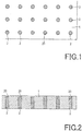
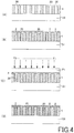
- a substrate 1 for an electronic device comprises a plurality of through electrodes 2 arranged at a given pitch of the order of ⁇ m.
- the via diameter of the through electrode 2 is also of the order of ⁇ m.
- the through electrode 2 has a nanocomposite structure including a nm-sized carbon nanotube and is a casting formed by using a via 20 formed in the substrate 1 as a mold.
- the through electrode 2 is a casting formed by using the via 20 formed in the substrate 1 as a mold, as described above, the substrate 1 can be provided with a through electrode 2 that has a high adhesion strength to a side wall surface of the via 20, a compact structure free from any cavity, void or hollow, a low electrical resistance and an excellent electrical conductivity. Even if the inner wall surface of the via 20 has irregularities, the through electrode 2 can be casted to conform to the irregularities, so that there can be obtained a through electrode 2 having a high adhesion strength to the via 20.
- the through electrode 2 can be casted to conform to the irregularities of the inner wall surface of the via 20, the through electrode 2 and the irregularities of the inner wall surface of the via 20 serve as an anchor for preventing slippage of the through electrode 2, thereby increasing the bonding strength of the through electrode 2 to the substrate 1.
- the inner wall surface of the via 20 does not require accuracy for the irregularities, but it is rather preferable to have certain irregularities. This makes it easy to form the via 20.
- the through electrode 2 is filled in the via 20 formed in the substrate 1 to have a compact structure free from any cavity, void or hollow, wherein the through electrode 2 is kept in close contact with the side wall surface of the via 20 even though the side wall surface of the via 20 has irregularities.
- the via 20 can be drilled by laser, chemical etching, plasma etching or the like and its inner wall surface has irregularities due to the via drilling process, but as shown in Fig. 3 , even though the inner wall surface of the via 20 has irregularities, the through electrode 2 is filled to conform to the irregularities and brought into close contact with the inner wall surface of the via 20 to have a compact structure free from any cavity, void or hollow. Moreover, since the irregularities of the inner wall surface of the via 20 create a kind of anchoring effect, the through electrode 2 can be reliably secured within the via 20 without causing loosening or floating from the via 20.
- the via 20 can be formed with less attention to the flatness of the inner wall surface, but rather a preferable result can be obtained by forming the via 20 with certain roughness.
- the through electrode 2 has a nanocomposite structure including a nm-sized carbon nanotube.
- the carbon nanotube is a material in which a six-member carbon ring (graphene sheet) is formed into a single- or multi-walled coaxial tube. Either a single-walled nanotube (SWNT) or a multi-walled nanotube (MWNT) can be used. More specifically, there can be used a composite material in which nm-sized carbon nanotubes are oriented and added as a filler into an aluminum alloy.
- the carbon nanotube has a high thermal conductivity which is 10 times greater than that of copper, providing extremely high heat dissipation characteristics.
- the carbon nanotube also has a high current density resistance of 10 9 A/cm 2 which is more than 1,000 times greater than that of copper.
- the carbon nanotube has less electron scattering as compared with copper being a good electrical conductor, it has a low electrical resistance.
- the through electrode 2 including a carbon nanotube has a low electrical resistance and can reduce the quantity of heat due to resistance even if a large current is passed.
- the carbon nanotube has a diameter of a few nm and is cut into a length of 500 nm or less, preferably, 200 to 300 nm, for use in the present invention.
- the through electrode 2 may comprise the carbon nanotube alone or a composite material including the carbon nanotube and a metal/alloy component having a nanocomposite crystal structure.
- the through electrode 2 having a nanocomposite structure including the nm-sized carbon nanotube and the metal/alloy component having a nanocomposite crystal structure includes a structure (crystal) whose size is limited to a nano level, stress that will be generated in the through electrode 2 can be reduced accordingly.
- the nanocomposite crystal structure is also capable of facilitating formation of equiaxed crystal in the vertical conductor.
- the above-described particular characteristics of the nanocomposite structure and the nanocomposite crystal structure inhibit characteristic degradation of a semiconductor circuit, particularly, in a semiconductor substrate. It can also inhibit the occurrence of fracturing or cracking of the substrate 1.
- the metal/alloy component having a nanocomposite crystal structure examples include Bi, In, Sn and Cu.
- the through electrode 2 can be formed compactly inside the via 20 without leaving any hollow or void because of volumetric expansion characteristics of Bi during the solidification.
- Bi since the presence of Bi tends to increase the electrical resistance, it is preferred that Bi is used to such an extent as to meet a required electrical resistance.
- It may also comprise a composite material prepared by mixing the nm-sized carbon nanotube with an organic material, wherein, if necessary, inorganic powder of ceramic, glass or the like or a metal/alloy component having a nanocomposite crystal structure may be added thereto.
- the substrate 1 supporting the through electrode 2 can include at least one of an inorganic substrate such as of ceramic, an organic substrate such as one used for a copper-clad substrate and a semiconductor substrate.
- an inorganic substrate such as of ceramic
- an organic substrate such as one used for a copper-clad substrate
- a semiconductor substrate Any type of semiconductor substrate can be used without particular limitation.
- the through electrode 2 is electrically insulated from the conductive inorganic substrate, the conductive organic substrate and the semiconductor substrate by an electrical insulating film or layer.
- This insulating structure can be realized by an insulating film obtained by oxidizing or nitriding the inner wall surface of the via 20 that will act as a mold for the through electrode 2 or an insulating layer adhered to the inner wall surface of the via 20.
- the above-described insulating layer may be provided in the form of a ring at a small distance around the via 20.
- a substrate 1 having a number of small vias 20 previously formed to pass through it in the thickness direction is put on a support S1.
- the via 20 is closed at its lower side by the support S1.
- the via 20 may be a non-through-hole.
- the vias 20 formed in the substrate 1 are used as a mold and an electrode material 2 in the form of liquid, paste or powder is poured into them.
- the electrode material 2 poured into the vias 20 is solidified while being subjected to a mechanical force F1 such as a pressing pressure using a pressing plate P1, an injection pressure or a rolling pressure.
- a mechanical force F1 such as a pressing pressure using a pressing plate P1, an injection pressure or a rolling pressure.
- the through electrode 2 can be formed as a casting having a compact structure free from any cavity, void or hollow and kept in close contact with the side wall surface of the via 20. It should be noted that the structure of the casting can be seen from the SEM image of Fig. 3 .
- the process of pouring the electrode material 2 into the vias 20 formed in the substrate 1 is performed inside a vacuum chamber under a reduced pressure. This is because differential pressure filling can be performed by using this reduced pressure and a pressure to be applied subsequently.
- the electrode material 2 has a nanocomposite structure including a carbon nanotube and a metal/alloy component having a nanocomposite crystal structure
- a liquid composite material 2 prepared by mixing a molten metal of the metal/alloy component with the nm-sized carbon nanotube is poured into the vias 20, and the poured liquid composite material 2 is cooled and solidified while being subjected to a pressing pressure using the pressing plate P1, an injection pressure or a rolling pressure.
- the electrode material 2 is a paste material including a carbon nanotube, an organic material and a solvent
- it is hardened by heating while being subjected to a pressing pressure using the pressing plate P1, an injection pressure or a rolling pressure.
- the electrode material 2 is a powder material, it may be poured into the vias 20 in a molten state or put in the vias 20 in a powder state and then melted by heating.
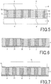
- Fig. 5 shows an electronic device in which the substrate shown in Figs. 1 and 2 is used as an interposer.
- the substrate 1 is disposed as an interposer between electronic devices 6, 6 such as a semiconductor chip.
- the electronic devices 6, 6 have electrodes connected to the through electrode 2 through junction films 4, 4, respectively.
- the two or more separate through electrodes 2 can be used as a positive or negative electrode for the electronic devices 6, 6 to be mounted on the substrate 1. Therefore, electrical wiring such as wire bonding becomes unnecessary, so that the product cost can be reduced by cutting the production facility cost that has been spent on an expensive wire bonding apparatus.
- the substrate 1 may comprise columnar heat sinks independently of or along with the through electrodes 2. Referring first to Fig. 6 , the substrate 1 has columnar heat sinks 3.
- the columnar heat sink 3 is a casting formed by using a via 30 formed in the substrate 1 as a mold. Many columnar heat sinks 3 passing through the substrate 1 in the thickness direction are arranged at a small distance from each other, for example, in the form of matrix.
- the columnar heat sinks 3 have first ends (lower ends) connected together through a heat dissipation layer 31 provided on a back surface (second surface) of the substrate 1 and second ends (upper ends) led to a front surface of the substrate 1. Another heat dissipation layer may also be provided on the front surface.
- the columnar heat sink 3 is electrically insulated from the conductive inorganic substrate, the conductive organic substrate and the semiconductor substrate by an electrical insulating film or layer.
- This insulating structure can be realized by an insulating film obtained by oxidizing or nitriding the inner wall surface of the via 30 that will act as a mold or an insulating layer adhered to the inner wall surface of the via 30.
- the above-described insulating layer may be provided in the form of a ring at a small distance around the via 30.
- the columnar heat sink 3 is also a casting formed by using the via 30 formed in the substrate 1 as a mold, the substrate 1 can be provided with a columnar heat sink 3 that has a high adhesion strength to the side wall surface of the via 30, a compact structure free from any cavity, void or hollow and excellent thermal conductivity and heat dissipation characteristics.
- the columnar heat sink 3 having a high adhesion strength to the side wall surface of the via and a compact structure free from any cavity, void or hollow can be formed efficiently in a short time, as compared with the case where it is formed by using another method such as plating.
- the inner wall surface of the via 30 has to be a smooth surface having extremely small irregularities so as to form a continuous plating film, which will need a long time for the via formation process. Moreover, if the via 30 has a high aspect ratio, it becomes extremely difficult to form a plating primary film as a continuous homogeneous film.
- the columnar heat sink 3 is a casting formed by using the via 30 formed in the substrate 1 as a mold
- the columnar heat sink 3 can be filled to conform to the irregularities in the course of casting. Therefore, the obtained columnar heat sink 3 has a compact structure free from any cavity, void or hollow and in close contact with the side wall surface of the via 30. This realizes a columnar heat sink 3 having an excellent thermal conductivity and heat dissipation characteristics.
- the columnar heat sink 3 can be reliably secured within the via 30 without causing loosening or floating from the via 30.
- the heat dissipation characteristics of the columnar heat sinks 3 depend on the thermal conductivity (or thermal resistance) of the constituent material and the total occupancy rate of the columnar heat sinks 3 to a plane area of the substrate 1. For example, if a low-thermal resistance material is used for the columnar heat sink 3, the occupancy rate can be reduced, while if a high-thermal resistance material is used, the occupancy rate can be increased. That is, the occupancy rate of the columnar heat sinks 3 can be determined in consideration of the thermal conductivity of the constituent material. On the other hand, if there is a limit to the occupancy rate, materials having a suitable thermal conductivity can be selected in consideration of required heat dissipation characteristics.
- the columnar heat sink 3 can have a nanocomposite structure including a metal/alloy component having a nanocomposite crystal structure. This results in reducing stress that will be generated in the columnar heat sink 3. Moreover, since the nanocomposite crystal structure is also capable of facilitating formation of equiaxed crystal in the columnar heat sink 3, the stress can be further reduced.
- the above-described particular characteristics of the nanocomposite crystal structure inhibit characteristic degradation of a semiconductor circuit formed on the substrate 1. It can also inhibit the occurrence of fracturing or cracking of the substrate 1.
- the nanocomposite crystal structure material constituting the columnar heat sink 3 include, but not limited to, Al, Au, Cu, Ag and Sn. However, since it is desirable to reduce the thermal resistance of the columnar heat sink 3 as much as possible, the material, composition ratio and so on should be determined from such a viewpoint.
- the columnar heat sink 3 is a solid column having a circular section, but it may have a polygonal section.
- the columnar heat sink 3 may include a nm-sized carbon atom structure having an excellent thermal conductivity along with or independently of the metal/alloy component having a nanocomposite crystal structure. At least one of a diamond, a fullerene and a carbon nanotube can be given as a specific example of such a carbon atom structure.
- the columnar heat sink 3 including the carbon atom structure has excellent heat dissipation characteristics because of the high thermal conductivity of the carbon atom structure.
- the carbon nanotube has a high thermal conductivity which is 10 times greater than that of copper, ensuring extremely high heat dissipation characteristics.
- a material in which carbon nanotubes are oriented and added as a filler into an aluminum alloy In combination with the carbon nanotubes, vapor-grown carbon fibers having a larger fiber thickness may also be used as a filler.
- This composite material has a thermal conductivity which is more than 3 times greater than that of the aluminum alloy.
- the carbon nanotube is cut into a length of 500 nm or less, preferably, 200 to 300 nm.
- the heat dissipation substrate according to the present invention is provided with a heat-generating electronic component and used to dissipate the heat to the outside.
- Fig. 7 shows one embodiment of such an electronic device.
- a heat-generating electronic component or electronic device 6 is mounted through a thermally conductive binder layer 51.
- a heat dissipation block is thermally coupled to the heat dissipation 31.
- the electronic component or electronic device 6 is, for example, an active element such as a semiconductor chip, a passive component such as a capacitor or an inductor or a composite element thereof.
- the electronic component or electronic device 6 may have a semiconductor element and a passive component in combination or may be a memory element, a logic circuit element or an analog circuit element. It may have a single layer structure or a multilayer structure of such elements.
- the substrate 1 according to the present invention has the columnar heat sink 3 being a casting formed by using the via 30 as a mold, and the columnar heat sink 3 creates a heat dissipation pathway that is in close contact with the side wall surface of the via 30 and has a compact structure free from any cavity, void or hollow and excellent thermal conductivity and heat dissipation characteristics.
- heat generated at the electronic component or electronic device 6 can be efficiently and reliably dissipated through the columnar heat sink 3 having an excellent thermal conductivity and heat dissipation characteristics, thereby avoiding abnormal heat generation, thermal runaway or malfunction of the electronic component or electronic device 6.
- the illustrated substrate 1 comprises both the through electrode 2 and the columnar heat sink 3.
- the through electrode 2 and the columnar heat sink 3 may be combined as follows.
- the above-described substrate 1 can be combined with an electronic component 6 to provide an electronic device.
- the electronic component 6 is mounted on the substrate 1 with its electrode bonded to the through electrode 2.
- an electrical circuit can be made for the electronic component 6 using the through electrode 2 having a low electrical resistance, while heat generated by the operation of the electronic component 6 can be efficiently dissipated through the columnar heat sink 3, thereby avoiding characteristic change, malfunction and even thermal runaway due to the heat generation of the electronic component 6.
- the electronic component may be an active element, a passive component or a composite element thereof.
- the active element include a light-emitting diode, various types of memories, various types of logic ICs and an analog circuit element.
- the passive component include a capacitor, an inductor, a resistor or a composite element thereof.
- the electronic device may be almost any electrical product based on the technology of the electronics. Specific examples include a personal computer, a mobile phone, a digital appliance, a light-emitting device using a light-emitting diode, a lighting apparatus, a traffic light, an image processing device, an image sensor and a vehicle-mounted electronic device. It may also be one having a three-dimensional multilayer structure based on the TSV technology or one having a three-dimensional multilayer structure constructed by combining an interposer and various types of elements.
- through electrodes and columnar heat sinks have the same features and effects as described above, so that duplicate explanations are omitted.
- a light-emitting device shown in Figs. 10 to 12 comprises a substrate 1 and a light-emitting element 6.
- the light-emitting element 6 is covered with a fluorescent layer 7.
- the substrate 1 serves as a so-called package, includes two through electrodes 2, 2 and a number of columnar heat sinks 3 and has a cavity 11 at one side thereof.
- the substrate 1 includes Si as a main component.
- the substrate 1 may be an insulating resin substrate or an insulating ceramic substrate.
- the substrate 1 has a rectangular outline but its shape is arbitrary.
- the cavity 11 of the substrate 1 is formed to surround the through electrodes 2, 2 at a distance, wherein a reflection film 8 such as an Al film, an Ag film or a Cr film is formed almost all along its inner side face by sputtering or the like. It is also possible to form an insulating film such as an oxide film beneath the reflection film 8.
- a reflection film 8 such as an Al film, an Ag film or a Cr film is formed almost all along its inner side face by sputtering or the like. It is also possible to form an insulating film such as an oxide film beneath the reflection film 8.
- the through electrodes 2, 2 each pass through the substrate 1 in the thickness direction within the area of the cavity 11 to have one end exposed on one side within the cavity 11 and the other end exposed on the other side of the substrate 1.
- the through electrodes 2, 2 are a solid column and may have any arbitrary section such as a polygonal shape or a circular shape.
- the through electrodes 2, 2 may have different planar shapes between a portion passing through the substrate 1 and a portion located on one surface of the substrate 1 and intended to be bonded to the light-emitting element 6.
- the portion passing through the substrate 1 is shaped to have a polygonal section, a circular section or the like, while the portion intended to be bonded to the light-emitting element 6 is shaped to have an increased plane area.
- the through electrodes 2, 2 preferably have an end face shaped in accordance with an electrode of a light-emitting element 6 to be connected.
- one of the through electrodes 2, 2 has a circular end face, while the other has a rectangular end face.
- the columnar heat sinks 3 passing through the substrate 1 in the thickness direction are arranged at a small distance from each other in the form of matrix.
- the columnar heat sinks 3 are connected together through a heat dissipation layer 31 provided on a back surface (second surface) of the substrate 1.
- the through electrodes 2, 2 are independent of the heat dissipation layer 31.
- the heat dissipation layer 31 is not limited to the illustrated film form but may have a three-dimensional structure having an enlarged heat dissipation area.
- the light-emitting element 6 is a light-emitting diode, and the one illustrated in Figs. 13 and 14 has a semiconductor multilayer structure 61 in which a P-type semiconductor layer 611 and an N-type semiconductor layer 613 are stacked on a surface opposite from a light-emitting surface 60 of a transparent crystal layer 62. Between the P-type semiconductor layer 611 and the N-type semiconductor layer 613 is disposed an active layer 612.
- the N-type semiconductor layer 613 lying closer to the transparent crystal layer 62 has a portion 614 not coinciding with the P-type semiconductor layer 611, and an N-side electrode 63 is disposed on the surface of the noncoinciding portion 614.
- a P-side electrode 64 is disposed on the surface of the P-type semiconductor layer 611 at a coinciding portion.
- the N-side electrode 63 is not limited to the circular shape but may have a polygonal shape.
- the plane area of the N-side electrode 63 disposed on the noncoinciding portion 614 is smaller than that of the P-side electrode 64 disposed on the coinciding portion.
- the N-side electrode 63 has a smaller electrode width than the P-side electrode 64.
- Figs. 13 and 14 show just an example of the light-emitting element 6 applicable to the present invention, and it should not be construed as limitative.
- it may be constructed such that the transparent crystal layer 62 and the semiconductor multilayer structure 61 are in an upside down relationship.
- the electrode area can be determined in consideration of current diffusion.
- the light-emitting element 6 is disposed within the cavity 11 of the substrate 1, wherein the P-side electrode 64 of the P-type semiconductor layer 611 is connected to one end of one through electrode 2, while the N-side electrode 63 of the N-type semiconductor layer 613 is connected to one end of the other through electrode 2.
- the light-emitting element 6 is disposed with its upper surface lower than the surface of the substrate 1 around the cavity 11. Then, the fluorescent layer 7 is filled therein in such a manner as to eliminate the gap.
- the P-side electrode 64 and the N-side electrode 63 are opposed to each other at a distance.
- a junction film is interposed at a junction interface between them.
- the junction film comprises at least one low-melting point metal component selected from the group consisting of Sn, In, Bi Ga and Sb and a high-melting point metal material including at least one component selected from the group consisting of Cr, Ag, Cu, Au, Pt, Pd, Ni, an Ni-P alloy and an Ni-B alloy. Since the low-melting point metal can be consumed by reacting with the P-side electrode 64 and one through electrode 2 or the N-side electrode 63 and the other through electrode 2 and forming an intermetallic compound, the melting point increases considerably after the bonding.
- the transparent crystal layer 62 comprises sapphire and its one side becomes the light-emitting surface 60.
- a buffer layer (not shown) lies on one side of the transparent crystal layer 62, and the semiconductor multilayer structure 61 is grown over the transparent crystal layer 62 with the buffer layer therebetween.
- the semiconductor multilayer structure 61 is well-known regarding the light-emitting element 6. It has a PN junction and typically comprises a III-V group compound semiconductor. However, it is not limited to the known art but can comprise any compound semiconductors that may be suggested in future.
- the light-emitting element 6 may be any one of red, green, blue and orange light-emitting elements or a white light-emitting element.
- Semiconductor materials for constituting the semiconductor multilayer structure 61 in these light-emitting elements and their manufacturing methods are well known in the art.
- the substrate 1 includes two through electrodes 2, 2 and has the cavity 11 at one side thereof.
- the through electrodes 2, 2 each pass through the substrate 1 in the thickness direction to have one end exposed on one side within the cavity 11.
- the light-emitting element 6 is disposed within the cavity 11 of the substrate 1.
- the light-emitting element 6 is constructed such that the P-type semiconductor layer 611 and the N-type semiconductor layer 613 are stacked on the second surface opposite from the first surface 60 which will become the light-emitting surface of the transparent crystal layer 62.
- the P-side electrode 64 of the P-type semiconductor layer 611 is connected to one end of one through electrode 2, while the N-side electrode 63 of the N-type semiconductor layer 613 is connected to one end of the other through electrode 2. According to the present embodiment, therefore, current can be supplied to the light-emitting element 6 from the side opposite from the side having the transparent crystal layer 62, thereby realizing a structure in which the electrodes for the light-emitting element 6 do not appear on the light-emitting surface 60. Thus, produced light can be efficiently emitted to the outside.
- the substrate 1 includes many columnar heat sinks 3.
- the columnar heat sinks 3 are provided to extend in the thickness direction of the substrate 1. Accordingly, heat generated by the light emitting operation of the light-emitting element 6 can be dissipated to the outside of the substrate 1 through the columnar heat sinks 3, keeping the bonding strength at the junction where the electrodes 63, 64 of the light-emitting element 6 are connected to the through electrodes 2, 2 and maintaining the reliability of electrical connection. Moreover, a variation in light-emitting characteristics of the light-emitting element 6 due to the heat generation can be avoided.
- the columnar heat sink 3 has one end led to the second surface of the substrate 1 and connected to the heat dissipation layer 31 provided on the second surface of the substrate 1. With this structure, the heat dissipation characteristics can be further improved.
- the reflection film 8 is provided between the inner surface of the cavity 11 and the side face of the light-emitting element 6. Therefore, light produced at the semiconductor layer 61 can be led to the light-emitting surface 60 of the transparent crystal layer 62 while suppressing light scattering and absorption due to the transparent crystal layer 62.
- the reflection film 8 may be adhered to the inner surface of the cavity 11 or adhered to the side face of the light-emitting element 6.
- the light-emitting element 6 is fitted in the cavity 11 with a small clearance. With this structure, positioning and setting of the light-emitting element 6 with respect to the substrate 1 can be performed easily and reliably.
- the light-emitting surface 60 may have a transparent optical component having small irregularities. This enables the light-emitting surface 60 to diffuse or disperse light, achieving uniform surface light emission. Instead of providing the transparent optical component, it is also possible to form the light-emitting surface 60 with small irregularities. Although not illustrated, furthermore, the light-emitting surface 60 may have a fluorescent body along with or without the small irregularities.
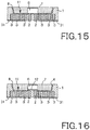
- a light-emitting device whose cavity 11 has an increased plane area as compared with the embodiment shown in Figs. 10 to 12 .
- the cavity 11 is considerably larger than the plane area of the light-emitting element 6, wherein the fluorescent layer 7 or the like is filled in a space between the periphery of the light-emitting element 6 and the inner wall surface of the cavity 11.
- the reflection film 8 is adhered to the inner wall surface of the cavity 11.
- the columnar heat sink 3 has one end (upper end) terminated at almost the same height as the bottom face of the cavity 11 and the other end led to the back surface of the substrate 1 and connected to the heat dissipation layer 31.
- Fig. 16 there is illustrated a light-emitting device having almost the same structure as that of Fig. 15 , wherein a protrusion 12 is provided at the center of the cavity 11 and the light-emitting element 6 is mounted on the protrusion 12.
- the embodiments of Figs. 15 and 16 also have the effects described with reference to Figs. 10 to 13 .
- the light-emitting device has numerous uses such as a light-emitting diode being a single light-emitting element, a surface light-emitting device having a plurality of light-emitting elements arranged, for example, in the form of matrix, a lighting apparatus, a backlight for a liquid crystal display, a signal light and so on. Their examples will be described below.
- Fig. 17 is a plan view of a lighting apparatus having a light-emitting diode.
- the illustrated lighting apparatus has a rectangular substrate 1 and a plurality of light-emitting devices Q arranged on the substrate 1 in the form of matrix.
- the light-emitting devices Q each have a light-emitting element 6 for emitting a light of a given hue, two through electrodes 2, 2 for electrical connection of the light-emitting element 6 and many columnar heat sinks 3 arranged around the light-emitting element 6.
- Each light-emitting element 6 is disposed within a cavity 11 formed in the substrate surface of a substrate 1.
- the shape of the substrate 1, the number and arrangement of the light-emitting devices Q and the number and arrangement of the columnar heat sinks 3 are not limited to the embodiment shown in Fig. 17 but can be determined as appropriate.
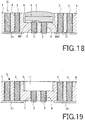
- the above-described light-emitting devices Q are shown in more detail in Figs. 18 to 20 .
- the substrate 1 serves as a so-called package, including a plurality of through electrodes 2 and a plurality of columnar heat sinks 3 and having cavities 11 in its substrate surface.
- a substrate including Si as a main component, but it is not limited thereto and an insulating resin substrate or an insulating ceramic substrate may also be used.
- it may be a conductive substrate such as a metal substrate. In the present embodiment, description will be made concerning the case where the substrate 1 is an Si substrate.
- the shape of the cavity 11 of the substrate 1 is not limited to the cuboid shape shown in Fig. 17 , but it may have other shapes.
- the cavity 11 is formed to surround the through electrodes 2, 2 at a distance as seen in plan, wherein a reflection film 8 is formed almost all along its inner side face by sputtering or the like.
- the reflection film 8 is not limited to the above embodiment but may be adhered to the side face of the light-emitting element 6, for example, and it is also possible to form an insulating film such as an oxide film beneath the reflection film 8.
- the light-emitting element 6 is fitted in the cavity 11 with a small clearance. With this structure, positioning and setting of the light-emitting element 6 with respect to the substrate 1 can be performed easily and reliably. Moreover, the upper surface of the light-emitting element 6 within the cavity 11 is covered with the fluorescent layer 7. This improves the luminance of light emitted from the light-emitting element 6.
- fluorescent materials to be used for the fluorescent layer 7 include calcium phosphate.
- the hue of the fluorescent layer 7 may be determined as appropriate depending on the intended use.
- the through electrodes 2, 2 each pass through the substrate 1 in the thickness direction in the bottom face of the cavity 11 to have one end exposed on one side within the cavity 11 and the other end exposed on the other side of the substrate 1.
- the through electrodes 2, 2 may have an end face shaped in accordance with an electrode of the light-emitting element 6 to be connected, and in this case, the through electrodes 2, 2 have a circular end face and a rectangular end face, respectively.
- the through electrodes 2, 2 are electrically insulated from the substrate 1.
- an electrical insulating layer 9 is provided between the periphery of the through electrodes 2, 2 and the inner wall surface of the vias containing the through electrodes 2, 2.
- the electrical insulating layer 9 may be an oxide film or a nitride film obtained by oxidizing or nitriding the inner wall surface of the via in the substrate 1 being an Si substrate or a layer of an organic insulating material or an inorganic insulating material such as glass filled into the via.
- the heat dissipation layer 31 comprises a material having a relatively high thermal conductivity such as aluminum and can be disposed on the back surface of the substrate 1 as a plurality of separate members or as a single member to be connected in common to all the heat sinks 3. Furthermore, the heat dissipation layer 31 is not limited to the illustrated film form but may have a three-dimensional structure having an increased heat dissipation area.
- Fig. 20 shows another embodiment of the light-emitting devices Q.
- the difference between the light-emitting device according to the present embodiment and the foregoing embodiment resides in that the substrate 1 comprises three layers 101 to 103 and that the cavity 11 has an increased plane area.
- the substrate 1 is an SOI substrate constructed by stacking a first silicone layer 101 comprising a first substrate layer, an oxide layer 102 comprising an insulating layer, and a second silicon layer 103 comprising a second substrate layer in the mentioned order.
- the cavity 11 is formed by cutting off the surface of the second silicon layer 103 and has an inner side face which is inclined to increase the opening area toward the open end.
- the cavity 11 has a considerably larger plane area than the light-emitting element 6, wherein the fluorescent layer 7 is filled in a space between the periphery of the light-emitting element 6 and the inner wall surface of the cavity 11.
- the reflection film 8 is adhered to the inner wall surface of the cavity 11 as in the foregoing embodiment.
- the through electrodes 2, 2 pass through the first silicon layer 101 in an electrically insulated state because of the electrical insulating layer 9 and have their cavity 11-side ends connected to connections 41, 42 passing through the oxide layer 102, respectively.
- the connections 41, 42 are connected to two terminals 601, 602 of the light-emitting element 6.
- the connections 41, 42 are not limited to a cylindrical shape but may have other shapes such as a square pole shape.
- the columnar heat sinks 3 are provided to pass through the first silicone layer 101 in the thickness direction of the substrate 1 in the same manner as the through electrodes 2, 2 and connected to the heat dissipation layer 31. That is, the columnar heat sinks 3 are provided to extend from the back surface of the substrate 1 to the interface between the first silicon layer 101 and the oxide layer 102. With this structure, the oxide layer 102 can serve as an etching blocking layer during formation of the columnar heat sinks 3. This leads to an advantage that the etching process can be controlled extremely easily because the height of the columnar heat sink 3 can be defined by the film thickness of the first silicon layer 101.
- the above-described lighting apparatus includes the substrate 1, and the substrate 1 includes many columnar heat sinks 3. Since the columnar heat sinks 3 are provided to extend in the thickness direction of the substrate 1, heat generated by the light emitting operation of the light-emitting element 6 can be dissipated to the outside of the substrate 1 through the columnar heat sinks 3, keeping the bonding strength at the junction where the terminals 601, 602 of the light-emitting element 6 are connected to the through electrodes 2, 2 and maintaining the reliability of electrical connection, and also avoiding a variation in light-emitting characteristics of the light-emitting element 6 due to the heat generation.
- the columnar heat sink 3 has one end led to the second surface of the substrate 1 and connected to the heat dissipation layer 31 provided on the second surface of the substrate 1, the heat dissipation characteristics of the substrate 1 can be further improved.
- the light-emitting element 6 is the one shown in Figs. 13 and 14 . Therefore, current can be supplied to the light-emitting element 6 from the side opposite from the transparent crystal layer 62 in the stacking direction, thereby realizing a structure in which the terminals 601, 602 of the light-emitting element 6 do not appear on the light-emitting surface, so that produced light can be efficiently emitted to the outside. Moreover, the light produced at the semiconductor layer 61 can be effectively led to the light-emitting surface of the transparent crystal layer 62 because the reflection film 8 can suppress light scattering and absorption due to the transparent crystal layer 62.
- the liquid crystal display includes a liquid crystal panel 120 and a backlight 130.
- this liquid crystal display is not limited to a common display device for computers or a liquid crystal display for general-purpose appliances but can also be used for a liquid crystal television or a portable electronic device such as a mobile phone, a handheld game console or a personal digital assistant.
- the liquid crystal panel 120 is a liquid crystal module comprising a polarizing filter, a glass substrate, a liquid crystal layer and so on and driven by electrical signals from a driving circuit (not shown) based on image signals.
- the backlight 130 is the lighting apparatus shown in Figs. 17 to 21 and illuminates the liquid crystal panel 120 from the back side with a plurality of the light-emitting devices Q.
- the backlight 130 is not limited to this embodiment and, for example, may be the lighting apparatus shown in Figs. 10 to 16 , and it goes without saying that any type of lighting apparatus according to the present invention can be used.
- the through electrodes 2, 2 are connected to a power supply through a bump electrode and a wiring substrate, whereby the light-emitting element 6 supplied with power can irradiate light to the liquid crystal panel 120.
- the columnar heat sinks 3 are connected to the heat dissipation layer 31 so as to expel heat inside the substrate 1 toward the back surface of the liquid crystal display.
- the liquid crystal display according to the present invention also has the foregoing effects because of including the above-described lighting apparatus.
- the light-emitting diode display uses the light-emitting element itself as a pixel, it does not need a backlight and therefore has the advantage of being able to reduce power consumption.
- Fig. 23 shows a pixel Q of the light-emitting diode display as seen in plan
- Fig. 24 shows the light-emitting diode display in which the pixels Q are arranged in the form of matrix on the substrate 1.
- the single pixel Q has three light-emitting devices QR, QG, QB, wherein these light-emitting devices QR, QG, QB have a light-emitting element 6R for emitting a red light, a light-emitting element 6G for emitting a green light and a light-emitting element 6B for emitting a blue light, respectively.
- the light-emitting diode display according to the present embodiment is intended to be a full-color display and therefore includes the light-emitting elements 6R, 6G, 6B for three colors, but it is not limited thereto.
- the pixel Q may include only one of the light-emitting elements 6R, 6G, 6B for three colors. That is, the pixel Q can be constructed by appropriately selecting the light-emitting devices QR, QG, QB having a light-emitting element based on its display function.
- the three light-emitting devices QR, QG, QB are located at vertexes of a triangle as illustrated, but they are not limited thereto and may be arranged as appropriate depending on the characteristics of the light-emitting elements 6R, 6G, 6B for three colors.
- the through electrodes 2, 2 of each light-emitting element 6R, 6G, 6B are connected to a thin-film transistor (TFT) or the like, whereby light emission of each pixel Q is controlled by a driving circuit depending on image signals.
- the columnar heat sinks 3 are connected to the heat dissipation layer 31 so as to expel heat inside the substrate 1 toward the back surface of the display, as in the structure shown in Figs. 18 to 23 .
- the light-emitting diode display according to the present invention also has the foregoing effects because of having the same structure as the above-described lighting apparatus.
- the signal light according to the present invention is intended for use in a railroad signal or a traffic light, for example, and constructed by arranging many light-emitting devices QR, QG, QB to have the light-emitting elements 6R, 6G, 6B, for example, for two or more colors, as in the above-described light-emitting diode display.
- the signal light according to the present invention also has the foregoing effects because of having the same structure as the above-described lighting apparatus.
- the substrate 1 shown in Fig. 25 has the through electrodes 2, the columnar heat sinks 3 and the cavity 11.
- the illustrated substrate 1 is an SOI substrate constructed by stacking a first silicone layer 101 comprising a first substrate layer, an oxide layer 102 comprising an insulating layer, and a second silicon layer 103 comprising a second substrate layer in the mentioned order.
- SOI substrate SIMOX (separation by implantation of oxygen)-type and wafer bonding-type. Any type of SOI substrate can be used.
- SIMOX-type SOI substrate there has been known a technique of forming an insulating layer of oxidized silicon within a silicon crystal by burying oxygen molecules from the silicon crystal surface using ion implantation and then oxidizing it at a high temperature. Such an insulating layer is referred to as buried oxide (BOX) layer.
- BOX buried oxide
- the cavity 11 is a portion to which an electronic element is to be attached and formed in the surface of the second silicon layer 103.
- the illustrated cavity 11 is formed by cutting off the center of the second silicon layer 103 in a rectangular shape and has an inner side face which is inclined to increase the opening area toward the open end.
- the second silicon layer 103 and the inner surface of the cavity 11 are covered with an insulating layer 132.
- the insulating layer 132 may be a silicon oxide film or a silicon nitride film.
- an insulating film 111 is provided between the first silicone layer 101 and the through electrode 2 and on the surface of the first silicone layer 101.
- the insulating film 111 may be a silicon oxide film or a silicon nitride film.
- the element-connecting portion 23 is adhered to one end of the through portion 22, while the other end passes through the insulating film 111, the oxide layer 102 and the insulating layer 132 adhered to the bottom face of the cavity 11 and projects into the cavity 11 for exposure.
- the element-connecting portion 23 may also be an electroless plating film such as of Ti-Au as with the terminal portion 21.
- the columnar heat sinks 3 are each filled in a via 113 formed in the thickness direction of the first silicone layer 101.
- the columnar heat sink 3 comprises a columnar portion 301 being a main part and a terminal portion 302 adhered to one end face thereof.
- the terminal portion 302 may be an electroless plating film such as of Ti-Au as with the terminal portion 21.
- the vias 113 having the columnar portion 301 are provided to pass through the first silicone layer 101 and terminate at the interface between first silicone layer 101 and the oxide layer 102 and are distributed around the cavity 11 to have a given occupancy rate as the substrate 1 is seen in plan.
- the insulating film 111 being a silicon oxide film or a silicon nitride film.
- a light-emitting device having the substrate 1 shown in Fig. 25 .
- a light-emitting element (LED) 6 being an electronic element is disposed in the cavity 11 of the circuit substrate.
- the light-emitting element 6 has an electrode bonded to the element-connecting portion 23 of the through electrode 2.
- the insulating layer 132 inside the cavity 11 is preferably provided with a light reflection film.
- the substrate 1 has the cavity 11 and the through electrodes 2, the cavity 11 is formed in the surface of the second silicon layer 103, and the through electrode 2 passes through the first silicon layer 101 and the oxide layer 102 to have one end exposed on the bottom face of the cavity 11. Therefore, the light-emitting element 6 being an electronic element can be disposed within the cavity 11 of the circuit substrate and the electrode provided on one surface of the light-emitting element 6 can be bonded to the element-connecting portion 23 forming one end of the through electrode 2. Thus, the light-emitting element 6 can be connected to the through electrode 2 by a flip chip bonding process.
- the circuit substrate according to the present invention includes the columnar heat sink 3, and the columnar heat sink 3 is filled in the via 113.
- the via 113 passes through the first silicon layer 101. Accordingly, heat generated by the operation of the light-emitting element 6 can be dissipated to the outside of the substrate 1 through the columnar heat sinks 3, keeping the bonding strength at the portion where the light-emitting element 6 is bonded to the through electrode 2 and maintaining the reliability of electrical connection. Moreover, a variation in electrical characteristics of the light-emitting element 6 due to the heat generation can be avoided.
- the via 113 is provided to pass through the first silicon layer 101 and terminate at the interface between the first silicon layer 101 and the oxide layer 102.
- the oxide layer 102 can serve as an etching blocking layer during formation of the via 113. This makes it extremely easy to control the depth of the via 113 because the depth of the via 113 has a uniform value defined by a depth from the first silicon layer 101 to the oxide layer 102, i.e., the film thickness of the first silicon layer 101.
- the vias 113 are distributed around the cavity 11 to have a given occupancy rate as the substrate 1 is seen in plan. This means that a heat dissipation area is formed to surround the electronic element housed in the cavity 11, i.e., the light-emitting element 6 with the columnar heat sinks 3, so that heat generated at the light-emitting element 6 can be collected and dissipated efficiently.
- Fig. 28 shows an electronic device in which an electronic element 6 is incorporated into the circuit substrate shown in Fig. 27 .
- the electronic element 6 has a three-dimensional multilayer structure based on the TSV technology, wherein a logic element 6A such as an LSI and a memory element 6C such as a DRAM are stacked and bonded through an interposer 6B.
- Electronic devices of this type can be used as a basic element of an information processing system. More specifically, they can be used as a component of an image processing system in a personal digital assistant, a mobile phone, a digital appliance, a server or the like. There are other uses, including an image sensor module.
- the logic element 6A is a so-called logic IC, and its electrodes provided on one side are bonded to the element-connecting portions 23 of the through elements 2 provided in the substrate 1.
- the logic element 6A is in the form of a chip containing a semiconductor logic circuit such as an LSI.
- the logic element 6A may have a three-dimensional multilayer structure in which the embedded semiconductor logic circuit is led to the electrodes based on the TSV technology.
- the interposer 6B has a plurality of through electrodes, wherein one end of the through electrode is connected to an electrode of the logic element 6A, while the other end of the through electrode is connected to an electrode of the memory element 6C.
- the interposer 6B can be obtained such that the through electrodes are formed in an Si substrate, a resin substrate or a ceramic substrate by using the same composition and manufacturing process as the through electrodes of the circuit substrate.
- the memory element 6C has an embedded memory cell connected to the electrode.
- the memory element 6C may also have a three-dimensional structure in which the memory cell is led to the electrodes based on the TSV technology as in the logic element 6A.
- Fig. 28 merely shows one conceptual example of the three-dimensional multilayer structure.
- the electronic device shown in Fig. 28 has the same effects as the electronic device shown in Fig. 26 .
- the electronic device of Fig. 28 since the three-dimensional multilayer structure is employed to improve the packaging density, the performance and the processing speed and reduce the size, the thickness and the weight, the question of how to dissipate heat generated by the operation becomes a more serious issue.
- Fig. 29 shows still another electronic device.
- the portions corresponding to the components illustrated in the foregoing figures are denoted by the same reference symbols and duplicate explanations are omitted.
- a plurality of through electrodes 2 each pass through the substrate 1 in the thickness direction within the area of the cavity 11 to have one end exposed on one side within the cavity 11 and the other end exposed on the other side of the substrate 1.
- the columnar heat sinks 3 passing through the substrate 1 in the thickness direction are arranged in the form of matrix at a small distance from each other.
- the columnar heat sinks 3 have first ends (lower ends) connected together through a heat dissipation layer 31 provided on the back surface (second surface) of the substrate 1 and second ends (upper ends) led to the front surface of the substrate 1.
- the heat dissipation layer 31 is not limited to the illustrated film form but may have a three-dimensional structure having an increased heat dissipation area.
- the illustrated electronic element 6 takes the form of a flip chip having a plurality of electrodes 601 on one surface intended to be a mounting surface and is disposed within the cavity 11 of the substrate 1 to have each electrode 601 bonded to one end of the through electrode 2.
- the illustrated electronic device includes the substrate 1, and the substrate 1 includes many columnar heat sinks 3.
- the columnar heat sinks 3 are provided to extend in the thickness direction of the substrate 1. Therefore, heat generated by the operation of the electronic element 6 can be dissipated to the outside of the substrate 1 through the columnar heat sinks 3, keeping the bonding strength at the junction where the electrodes 601 of the electronic element 6 are connected to the through electrodes 2 and maintaining the reliability of electrical connection. Moreover, a variation in electrical characteristics of the electronic element 6 due to the heat generation can be avoided.
- the substrate 1 has the cavity 11 at one side thereof and contains therein the electronic element 6.
- Many columnar heat sinks 3 each passing through the substrate 1 in the thickness direction are arranged around the cavity 11 to surround the cavity 11 at a small distance from each other. This means that a heat dissipation pathway is formed by the columnar heat sinks 3 to three-dimensionally surround the electronic element 6 housed in the cavity 11, so that heat generated at the electronic element 6 can be collected three-dimensionally and dissipated efficiently.
- the columnar heat sink 3 passes through the substrate 1 in the thickness direction to have one end led to the second surface of the substrate 1 and connected to the heat dissipation layer 31 provided on the second surface of the substrate 1. With this structure, the heat dissipation characteristics can be further improved.
- the electronic element 6 is fitted in the cavity 11 with a small clearance. With this structure, positioning and setting of the electronic element 6 with respect to the substrate 1 can be performed easily and reliably.
- the electronic element 6 has a three-dimensional multilayer structure based on the TSV technology, wherein a logic element 6A such as an LSI and a memory element 6C such as a DRAM are stacked and bonded through an interposer 6B. That is, it has a similar structure to that shown in Fig. 28 .
- the interposer 6B has many through electrodes 2B arranged at a distance from each other, wherein one end of the through electrode 2B is connected to an electrode 412 of the logic element 6A, while the other end of the through electrode 2B is connected to an electrode 431 of the memory element 6C.
- the interposer 6B can be obtained such that the through electrodes 2B are formed in an Si substrate, a resin substrate or a ceramic substrate by using the same composition and manufacturing process as the through electrodes 2.
- the columnar heat sink 3 passes through the substrate 1 in the thickness direction to have one end led to the second surface of the substrate 1 and connected to the heat dissipation layer 31 provided on the second surface of the substrate 1. With this structure, the heat dissipation characteristics can be further improved.
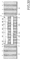
- Fig. 31 shows an electronic device 1 comprising a plurality of stacked substrates 101 to 103.
- the lowermost first substrate 101 is an Si substrate, a ceramic substrate, a glass-epoxy substrate or the like and intended to support the other substrates 102, 103.
- the second substrate 102 is an interposer located between the first substrate 101 and the third substrate 103 and includes a capacitor element 230 such as a decoupling capacitor.
- the third substrate 103 is an IC chip including an integrated circuit 233 such as an arithmetic element.
- the second and third substrates 102, 103 may be an Si substrate. It should be noted that since Fig. 31 shows a part of the multilayer structure on an enlarged scale, the IC chip is shown only partially.
- the first to third substrates 101 to 103 are stacked with their substrate surfaces in face-to-face contact with each other and include one or more through electrodes 2.
- the through electrode 2 is a continuous conductor extending across the first to third substrates 101 to 103. More specifically, the through electrode 2 is provided in the first to third substrates 101 to 103 in an embedded state to continuously pass through them in the stacking direction.
- all the through electrodes 2 continuously pass through the first to third substrates 101 to 103, but it is also possible that some of them pass through only one or two substrates.
- they may include a through electrode passing through the first and second substrates 101, 102 but not passing through the third substrate 103.
- the through electrode 2 is electrically connected to the capacitor element 230 and the integrated circuit 233, individually.
- the capacitor element 230 comprises a dielectric layer 234, an upper electrode layer 232 and a lower electrode layer 236. With the dielectric layer 234 therebetween, the upper electrode layer 232 and the lower electrode layer 236 are extended and electrically connected to the right and left through electrodes 2 in the figure.
- the integrated circuit 233 is also electrically connected to the through electrodes 2 with electrodes 231, 235 extending to the right and left through electrodes 2. Such a connecting structure can be adopted when the capacitor element 230 is used as a decoupling capacitor for removing power noise of the integrated circuit 233, for example.
- the through electrodes 2 being a continuous conductor extending across two or more substrates 101 to 103 are provided with the substrate surfaces of the substrates 101 to 103 in face-to-face contact with each other. That is, the electronic device according to the present invention has a structure in which two or more of substrates 101 to 103 are stacked without using bumps. According to the present invention, therefore, there can be realized a high-quality, highly-reliable electronic device which solves all the problems due to the use of a bump bonding structure, such as difficulty in positioning, guarantee of bonding strength and guarantee of heat resistance.
- Fig. 32 shows another embodiment.
- the columnar heat sinks 3 are provided instead of or along with the through electrodes 2.
- the columnar heat sinks 3 are arranged around the integrated circuit 233. This means that a heat dissipation pathway is formed by the columnar heat sinks 3 to surround the integrated circuit 233 as the third substrate 103 is seen in plan, so that heat generated at the integrated circuit 233 can be collected and dissipated efficiently.
- the integrated circuit 233 is an arithmetic element to be used for a high-heat-generating CPU or the like, the provision of the columnar heat sinks 3 is particularly effective from the viewpoint of ensuring operation stability or the like.
- the columnar heat sinks 3 are distributed with a given occupancy rate. By appropriately determining the occupancy rate of the columnar heat sinks 3 in consideration of the thermal resistance of the material constituting the columnar heat sinks 3, accordingly, heat generated by the operation of the integrated circuit 233 can be efficiently dissipated to the outside of the electronic device 1 through the columnar heat sinks 3, thereby avoiding abnormal heat generation.
- the columnar heat sink 3 is also a continuous body extending across two or more of the plurality of substrates 101 to 103, it makes it possible to solve all the problems that are inevitable when using a bump bonding structure for the columnar heat sinks 3, such as difficulty in positioning, guarantee of bonding strength and guarantee of heat resistance.
- a substrate having a number of columnar heat sinks 3 there is illustrated a substrate having a number of columnar heat sinks 3.
- the tip of the columnar heat sink 3 is kept within a heat-resistant insulating organic or inorganic substrate 1, thereby leaving an insulating layer having a thickness of ⁇ H1 above it. That is, the columnar heat sink 3 is not required to pass through it.
- the thickness of ⁇ H1 can be determined arbitrarily.
- a substrate 1 comprising an organic insulating substrate.
- the organic substrate 1 preferably comprises a heat-resistant material. Particularly preferred is one having a heat resistance of 300 °C or more.
- the organic substrate 1 has, on at least one side thereof, a metal layer 31, 32 such as of a Cu foil.
- the illustrated organic substrate 1 is a double-sided copper-clad substrate having the metal layers 31, 32 of a Cu foil on both sides thereof.
- Various types of such a double-sided copper-clad substrate are supplied from different board makers and put on the market, for example, under the name of high heat resistance glass-epoxy copper-clad substrate, high heat resistance low thermal expansion glass fabric base material epoxy resin copper-clad substrate, high thermal conductivity glass composite substrate, high heat resistance paper phenol copper-clad substrate, paper base phenolic resin copper-clad substrate and so on.
- the use of the organic substrate 1 has advantages that a circuit substrate that has been already put into practical use and commercially available can be utilized, that the material cost for the substrate can be reduced and that the via drilling process for the columnar heat sinks 3 can be performed in short time.
- the metal layer 31, 32 is provided on at least one side thereof, the surface of the organic substrate 1 can be prevented from coming into direct contact with and being thermally damaged by a molten metal by feeding the molten metal from the side having the metal layer 31, 32 during a common process including a heat treatment in the columnar heat sink-forming process.
- the metal layer 31, 32 is provided on a plane perpendicular to the columnar heat sinks 3, there is created not only a heat dissipation pathway in the thickness direction because of the columnar heat sinks 3 but also a heat dissipation and diffusion surface perpendicular to the heat dissipation pathway because of the metal layer 31, 32. That is, a three-dimensional heat dissipation pathway can be formed to improve the heat dissipation characteristics.
- a heat dissipation substrate having a structure in which a plurality of organic substrates 1 having a metal layer 31, 32 on at least one side thereof are stacked with the metal layers 31, 32 located at an interface.
- the number of organic substrates 1 to be stacked can be determined arbitrarily.
- adjacent organic substrates 1 are bonded together through a bonding material having an excellent heat resistance and thermal conductivity.
- the metal layers 31, 32 to be used as a heat dissipation pathway are provided at a middle portion of the stacked organic substrates 1, there is created a three-dimensional heat dissipation structure in which in addition to heat dissipation through the columnar heat sinks 3, heat transferred from the columnar heat sinks 3 can be dispersed in a planar direction at the middle portion of the substrates 1.
- heat can be prevented from being accumulated within the substrates 1, thereby suppressing temperature rise of an electronic component to be mounted on the substrates 1.
- the columnar heat sinks 3 are connected to the columnar heat sinks 3 and directly thermally coupled together.
- Figs. 33 to 35 are useful as a heat dissipation substrate, but they may have various forms in addition to those shown in Figs. 33 to 35 . Such examples are shown in Figs. 36 to 38 . In the figure, the portions corresponding to the components illustrated in Figs. 33 to 35 are denoted by the same reference symbols and duplicate explanations are omitted.
- Fig. 36 shows an embodiment in which the columnar heat sinks 3 are arranged at different pitches in two stacked organic substrates 1.
- Fig. 37 shows an embodiment in which only one of two stacked organic substrates 1 is provided with the columnar heat sinks 3, while the other is a heat-resistant insulating substrate having no columnar heat sink.
- Fig. 38 shows a heat dissipation substrate in which a plurality of organic substrates 1 having the columnar heat sinks 3 along with the metal layers 31, 32 on both sides thereof are stacked, and an organic substrate 1 having no columnar heat sink 3 is further stacked thereon.
- the heat dissipation substrate according to the present invention may be used exclusively as a heat dissipation means or may be used as a circuit substrate such as a mother board, a submount board or the like.
- a given number (two in the figure) of organic substrates 1 having the metal layers 31, 32 on both sides thereof are stacked, and areas A1, A2 for mounting an electronic component are defined in the bonded organic substrates 1, wherein through electrodes 2 to be exposed within the areas A1, A2 are provided to pass through the two organic substrates 1.
- the through electrode 2 has a bump on at least one end thereof.
- the areas A1, A2 and the through electrodes 2 can be designed depending on the type of an electronic component to be mounted.
- Figs. 41 and 42 show still another embodiment.
- the substrate 1 is a conductive substrate, and the columnar heat sinks 3 are electrically insulated from the conductive substrate 1 by an organic or inorganic insulating film 35 formed on an inner wall surface of the via 30 and one surface (lower surface) of the conductive substrate.
- the conductive substrate 1 may be a metal plate or an Si substrate.
- the through electrodes 2 are provided in addition to the columnar heat sinks 3.
- the through electrodes 2 are electrically insulated from the conductive substrate 1 by the insulating film 35.
- the electronic device according to the present invention may be almost any electrical product based on the technology of the electronics and its specific examples include a vehicle-mounted electronic device.
- vehicle-mounted electronic device examples include a motor drive inverter to be mounted on a hybrid vehicle or an electric vehicle, a large-scale integration device (LSI) for LED lamp control and so on.
- LSI large-scale integration device
- Fig. 43 is a circuit diagram of a motor driver unit including a motor drive inverter.
- the motor driver unit comprises a DC power supply 710, an inverter 730 and a controller 750 and is designed to drive a motor (or generator) 770 being a three-phase AC rotating electrical machine.
- the DC power supply 710 comprises, for example, a secondary cell such as a nickel-metal hydride cell or a lithium-ion cell, a capacitor, a condenser or a fuel cell.
- the inverter 730 comprises a U-phase arm 73U, a V-phase arm 73V and a W-phase arm 73W.
- the U-phase arm 73U comprises switching elements Q1, Q2 connected in series
- the V-phase arm 73V comprises switching elements Q3, Q4 connected in series
- the W-phase arm 73W comprises switching elements Q5, Q6 connected in series.
- diodes D1 to D6 for passing a current from the side of an emitter to the side of a collector are connected between the collector and the emitter of the switching elements Q1 to Q6, respectively.
- each phase arm is connected to a phase terminal of each phase coil U, V, W of the motor 770. That is, the motor 770 is constructed by commonly connecting one ends of U, V, W-phase three coils to its neutral point, while the other end of the U-phase coil is connected to a midpoint between the switching elements Q1, Q2, the other end of the V-phase coil is connected to a midpoint between the switching elements Q3, Q4 and the other end of the W-phase coil is connected to a midpoint between the switching elements Q5, Q6.
- the inverter 730 converts a direct current voltage supplied from the DC power supply 710 to an alternating current voltage based on a signal S1 from the controller 750 and drives the motor 770 with the alternating current voltage.
- the motor 770 can be driven to generate a torque in accordance with a torque command value.
- Fig. 44 is a drawing showing a mounted state of the switching element being a component of the inverter of the motor driver unit shown in Fig. 43 .
- the inverter 730 is mounted on one side of a heat dissipation substrate 1 according to the present invention.
- the U-phase arm 73U of the inverter 730 comprises the switching elements Q1, Q2, a P-electrode layer 63, an intermediate electrode layer 62 and an N-electrode layer 61. Since the V-phase arm 73V and the W-phase arm 73W have a similar structure, the following description will be made mainly for the U-phase arm 73U.
- the U-phase arm 73U comprises the switching elements Q1, Q2, the P-electrode layer 63, the intermediate electrode layer 62 and the N-electrode layer 61 and is mounted on one side of the heat dissipation substrate 1 according to the present invention.
- the P-electrode layer 63, the intermediate electrode layer 62 and the N-electrode layer 61 are all formed on the heat dissipation substrate 1 by patterning.
- One end of the P-electrode layer 63 is connected to a busbar forming a power-supply line LN1.
- One end of the N-electrode layer 61 is connected to a busbar forming a ground line LN2.
- the intermediate electrode layer 62 corresponds to the midpoint of the U-phase arm 73U in Fig. 43 .
- the busbars are also disposed on one side of the heat dissipation substrate 1.
- the switching element Q1 is adhered to the intermediate electrode layer 62 to bring the collector into conduction with the intermediate electrode layer 62.
- the emitter of the switching element Q1 is connected to the P-electrode layer 63 through a wire WL1.
- the switching element Q2 is adhered to the N-electrode layer 61 to bring the collector into conduction with the N-electrode layer 61.
- the emitter of the switching element Q2 is connected to the intermediate electrode layer 62 through a wire WL1.
- the heat dissipation substrate 1 is of the type having an insulating layer on one side (upper side) where the switching elements Q1, Q2, the P-electrode layer 63, the intermediate electrode layer 62 and the N-electrode layer 61 are to be mounted, while the metal layer 31 on the lower side is put on a heat dissipation block 50 through a silicone grease.
- the heat dissipation block 50 has a plurality of grooves 501.
- a water cooling system is used as a cooling system of the inverter 730, cooling water supplied from an external radiator (not shown) flows down the plurality of grooves 501 of the heat dissipation block 50 in a direction perpendicular to the plane of paper, thereby cooling the switching elements Q1, Q2 through the heat dissipation substrate 1.
- the switching elements Q3 to Q6 have the same cooling system.
- the heat dissipation substrate 1 In addition to the electrical insulation to the switching elements Q1, Q2, the P-electrode layer 63, the intermediate electrode layer 62, the N-electrode layer 61 and so on, the heat dissipation substrate 1 according to the present invention has a heat dissipation pathway formed by the columnar heat sinks 3, whereby heat of the switching elements Q1 to Q6 and the busbars constituting the inverter 730 can be efficiently transferred to the heat dissipation block 50, contributing to cooling of the switching elements Q1 to Q6, the busbars and so on.
- FIG. 45 an electronic component 6 is mounted on one side of the heat dissipation substrate 1 according to the present invention.
- the electronic component 6 is constructed by stacking and bonding a logic element 6A such as an LSI and a memory element 6C such as a DRAM through an interposer 6B.
- Electronic devices of this type can be used as a basic element of an information processing system. More specifically, they can be used as a component of an image processing system in a personal digital assistant, a mobile phone, a digital appliance, a server or the like. There are other uses, including an image sensor module.
- the logic element 6A is in the form of a chip containing a semiconductor logic circuit such as an LSI.
- the interposer 6B has a decoupling capacitor and a through electrode, wherein one end of the through electrode is connected to the logic element 6A, while the other end of the through electrode is connected to the memory element 6C.
- the interposer 6B can be obtained by forming the through electrode in an Si substrate, a resin substrate or a ceramic substrate.
- the layer number and type of the elements constituting the electronic component 6, the arrangement of their electrodes and so on can vary widely depending on the used electronic component 6, and Fig. 45 merely shows one conceptual example of the three-dimensional multilayer structure.
- the logic element 6A, the interposer 6B and the memory element 6C can also contain similar columnar heat sinks, wherein heat dissipation effect can be further improved by connecting the columnar heat sinks continuously and thermally coupling them to the columnar heat sinks 3 of the mother board 1.
- a submount board 1B containing the electronic component 6 is mounted on one side of a mother board 1A.
- the mother board 1A is similar to that shown in Fig. 19 and has a structure in which two organic substrates 101A, 102A having metal layers 31A, 32A on two sides thereof are stacked with the metal layers 31A, 32A located at an interface.
- the submount board 1B there are disposed not only columnar heat sinks 3B but also through electrodes 2B.
- the submount board 1B has a cavity 11 at one side thereof, and the columnar heat sinks 3B electrically insulated by an insulating layer 35B are provided in a thick portion around the cavity 11.
- One end of the columnar heat sink 3B is connected to a metal layer 31B.
- the through electrodes 2B are provided at the bottom of the cavity 11 and electrically insulated by the insulating layer 35B.
- the electronic component 6 is housed in the cavity 11, and electrodes (bumps) provided on the lower surface of the logic element 6A are connected to one ends of the through electrodes 2B.
- the submount board 1B has the cavity 11 at one side thereof and contains therein the electronic component 6.
- Many columnar heat sinks 3B each passing through the submount board 1B in the thickness direction are arranged around the cavity 11 at a small distance from each other. This means that a heat dissipation pathway is formed by the columnar heat sinks 3B to three-dimensionally surround the electronic component 6 housed in the cavity 11, so that heat generated at the electronic component 6 can be collected three-dimensionally and dissipated efficiently.
Landscapes
- Engineering & Computer Science (AREA)
- Microelectronics & Electronic Packaging (AREA)
- Manufacturing & Machinery (AREA)
- Cooling Or The Like Of Semiconductors Or Solid State Devices (AREA)
- Carbon And Carbon Compounds (AREA)
Claims (13)
- Substrat (1) comprenant une pluralité d'électrodes traversantes (2), les électrodes traversantes ayant une structure nanocomposite comportant un nanotube de carbone nanométrique et qui est une pièce moulée formée dans un trou d'interconnexion formé dans le substrat, caractérisé en ce que la structure nanocomposite comporte en outre un composant en métal/alliage ayant une structure cristalline nanocomposite.
- Substrat selon la revendication 1, comportant au moins l'un parmi un substrat inorganique, un substrat organique et un substrat semi-conducteur.
- Substrat selon la revendication 2, dans lequel le substrat inorganique et le substrat organique ont une conductivité électrique, et les électrodes traversantes sont isolées électriquement du substrat inorganique conducteur, du substrat organique conducteur et du substrat semi-conducteur par un film ou une couche d'isolation électrique.
- Substrat (1) comprenant une pluralité de dissipateurs thermiques colonnaires (3), les dissipateurs thermiques colonnaires ayant une structure nanocomposite comportant une structure en atome de carbone nanométrique et qui est une pièce moulée formée dans un trou d'interconnexion (30) formé dans le substrat, caractérisé en ce que la structure nanocomposite comporte en outre un composant en métal/alliage ayant une structure cristalline nanocomposite.
- Substrat selon la revendication 4, dans lequel la structure en atome de carbone comporte au moins l'un parmi un diamant, un fullerène et un nanotube de carbone.
- Substrat selon la revendication 4, comportant au moins l'un parmi un substrat inorganique, un substrat organique et un substrat semi-conducteur.
- Substrat selon la revendication 6, dans lequel le substrat inorganique et le substrat organique ont une conductivité électrique, et les dissipateurs thermiques colonnaires sont isolés électriquement du substrat inorganique conducteur, du substrat organique conducteur et du substrat semi-conducteur par un film ou une couche d'isolation électrique.
- Substrat selon la revendication 1, comprenant en outre une pluralité de dissipateurs thermiques colonnaires (3), les dissipateurs thermiques colonnaires étant une pièce moulée formée dans un trou d'interconnexion formé dans le substrat.
- Substrat selon la revendication 8, dans lequel les électrodes traversantes et les dissipateurs thermiques colonnaires ont une structure nanocomposite comportant un composant en métal/alliage ayant une structure cristalline nanocomposite.
- Substrat selon la revendication 9, dans lequel les dissipateurs thermiques colonnaires comportent une structure en atome de carbone nanométrique.
- Substrat selon la revendication 8, comprenant au moins l'un parmi un substrat inorganique, un substrat organique et un substrat semi-conducteur.
- Substrat selon la revendication 11, dans lequel le substrat inorganique et le substrat organique ont une conductivité électrique, et les électrodes traversantes ou les dissipateurs thermiques colonnaires sont isolés électriquement du substrat inorganique conducteur, du substrat organique conducteur et du substrat semi-conducteur par un film ou une couche d'isolation électrique.
- Dispositif électronique comprenant un substrat et un composant électronique, dans lequel le substrat est selon l'une quelconque des revendications 1 à 12, et le composant électronique est monté sur le substrat.
Applications Claiming Priority (7)
| Application Number | Priority Date | Filing Date | Title |
|---|---|---|---|
| JP2011000241 | 2011-01-04 | ||
| JP2011007519 | 2011-01-18 | ||
| JP2011015280A JP2012156369A (ja) | 2011-01-27 | 2011-01-27 | 回路基板、電子デバイス及びその製造方法 |
| JP2011034205A JP2012174826A (ja) | 2011-02-21 | 2011-02-21 | 電子デバイス及びその製造方法 |
| JP2011057542 | 2011-03-16 | ||
| JP2011092717A JP4880793B1 (ja) | 2011-04-19 | 2011-04-19 | 放熱部材及び電子機器 |
| JP2011118077 | 2011-05-26 |
Publications (3)
| Publication Number | Publication Date |
|---|---|
| EP2472577A2 EP2472577A2 (fr) | 2012-07-04 |
| EP2472577A3 EP2472577A3 (fr) | 2013-02-13 |
| EP2472577B1 true EP2472577B1 (fr) | 2017-09-27 |
Family
ID=45495701
Family Applications (1)
| Application Number | Title | Priority Date | Filing Date |
|---|---|---|---|
| EP11275161.5A Not-in-force EP2472577B1 (fr) | 2011-01-04 | 2011-12-15 | Substrat de dispositif électronique et dispositif électronique |
Country Status (5)
| Country | Link |
|---|---|
| US (1) | US9704793B2 (fr) |
| EP (1) | EP2472577B1 (fr) |
| KR (1) | KR20120079445A (fr) |
| CN (1) | CN102593100A (fr) |
| TW (1) | TW201234558A (fr) |
Families Citing this family (73)
| Publication number | Priority date | Publication date | Assignee | Title |
|---|---|---|---|---|
| KR20130101297A (ko) * | 2012-03-05 | 2013-09-13 | 삼성전자주식회사 | 반도체 발광소자 |
| US9496197B1 (en) * | 2012-04-20 | 2016-11-15 | Hrl Laboratories, Llc | Near junction cooling for GaN devices |
| DE102012105110A1 (de) * | 2012-06-13 | 2013-12-19 | Osram Opto Semiconductors Gmbh | Montageträger und Verfahren zur Montage eines Montageträgers auf einem Anschlussträger |
| CN104272446B (zh) | 2012-08-30 | 2016-11-09 | 松下知识产权经营株式会社 | 电子部件封装体及其制造方法 |
| JP5651807B2 (ja) | 2012-09-05 | 2015-01-14 | パナソニックIpマネジメント株式会社 | 半導体装置およびその製造方法 |
| DE102013101529A1 (de) | 2012-09-24 | 2014-03-27 | Osram Opto Semiconductors Gmbh | Optoelektronisches Bauelement und Verfahren zur Herstellung eines optoelektronischen Bauelements |
| KR20140041243A (ko) * | 2012-09-27 | 2014-04-04 | 삼성전자주식회사 | 발광소자 패키지 및 패키지 기판 |
| SG10201708630YA (en) * | 2013-02-21 | 2017-12-28 | Advanpack Solutions Pte Ltd | Semiconductor structure and method of fabricating the same |
| US9209136B2 (en) | 2013-04-01 | 2015-12-08 | Intel Corporation | Hybrid carbon-metal interconnect structures |
| WO2014184825A1 (fr) | 2013-05-15 | 2014-11-20 | 国立大学法人東北大学 | Procédé de traitement de surface de la paroi interne de microchambre vide |
| JP6186933B2 (ja) | 2013-06-21 | 2017-08-30 | 富士通株式会社 | 接合シート及びその製造方法、並びに放熱機構及びその製造方法 |
| KR101983142B1 (ko) * | 2013-06-28 | 2019-08-28 | 삼성전기주식회사 | 반도체 패키지 |
| JP2015029055A (ja) * | 2013-06-28 | 2015-02-12 | 株式会社デンソー | 電子装置 |
| US9461190B2 (en) * | 2013-09-24 | 2016-10-04 | Optiz, Inc. | Low profile sensor package with cooling feature and method of making same |
| FR3011383B1 (fr) * | 2013-09-30 | 2017-05-26 | Commissariat Energie Atomique | Procede de fabrication de dispositifs optoelectroniques a diodes electroluminescentes |
| US9565748B2 (en) * | 2013-10-28 | 2017-02-07 | Flextronics Ap, Llc | Nano-copper solder for filling thermal vias |
| JP6197619B2 (ja) | 2013-12-09 | 2017-09-20 | 富士通株式会社 | 電子装置及び電子装置の製造方法 |
| JP6176224B2 (ja) * | 2013-12-25 | 2017-08-09 | 日亜化学工業株式会社 | 半導体素子及びそれを備える半導体装置、並びに半導体素子の製造方法 |
| KR102111022B1 (ko) * | 2014-01-17 | 2020-05-15 | 삼성디스플레이 주식회사 | 유기 발광 표시 장치 및 그 제조 방법 |
| KR102166048B1 (ko) * | 2014-03-20 | 2020-10-15 | 엘지디스플레이 주식회사 | 다층회로기판 |
| US9524917B2 (en) * | 2014-04-23 | 2016-12-20 | Optiz, Inc. | Chip level heat dissipation using silicon |
| JP2015211204A (ja) * | 2014-04-30 | 2015-11-24 | イビデン株式会社 | 回路基板及びその製造方法 |
| US9455214B2 (en) | 2014-05-19 | 2016-09-27 | Globalfoundries Inc. | Wafer frontside-backside through silicon via |
| DE102014114982B4 (de) * | 2014-10-15 | 2023-01-26 | Infineon Technologies Ag | Verfahren zum Bilden einer Chip-Baugruppe |
| US9472483B2 (en) | 2014-12-17 | 2016-10-18 | International Business Machines Corporation | Integrated circuit cooling apparatus |
| US9184112B1 (en) | 2014-12-17 | 2015-11-10 | International Business Machines Corporation | Cooling apparatus for an integrated circuit |
| CN104576910B (zh) * | 2015-01-05 | 2017-08-01 | 福建天电光电有限公司 | 发光半导体器件的制造方法 |
| US9812375B2 (en) * | 2015-02-05 | 2017-11-07 | Ii-Vi Incorporated | Composite substrate with alternating pattern of diamond and metal or metal alloy |
| JP6533680B2 (ja) * | 2015-03-20 | 2019-06-19 | 新光電気工業株式会社 | 配線基板、半導体装置及び配線基板の製造方法 |
| JP2016219683A (ja) | 2015-05-25 | 2016-12-22 | ソニー株式会社 | 配線基板、および製造方法 |
| TWM519879U (zh) * | 2015-08-03 | 2016-04-01 | 道登電子材料股份有限公司 | 電子裝置之改良散熱結構 |
| KR102413224B1 (ko) | 2015-10-01 | 2022-06-24 | 쑤저우 레킨 세미컨덕터 컴퍼니 리미티드 | 발광 소자, 발광 소자 제조방법 및 발광 모듈 |
| US10199533B2 (en) * | 2015-12-21 | 2019-02-05 | Nichia Corporation | Method of manufacturing light emitting device |
| DE102016108427A1 (de) * | 2016-05-06 | 2017-11-09 | Epcos Ag | Multi-LED System |
| JP6708498B2 (ja) * | 2016-07-07 | 2020-06-10 | 昭和電工株式会社 | 冷却器及びその製造方法 |
| US10580567B2 (en) * | 2016-07-26 | 2020-03-03 | Samsung Electro-Mechanics Co., Ltd. | Coil component and method of manufacturing the same |
| CN106128640A (zh) * | 2016-08-23 | 2016-11-16 | 汉舟四川铜铝复合科技有限公司 | 一种高强度铜铝界面合金复合母线的制备工艺 |
| WO2019004264A1 (fr) * | 2017-06-30 | 2019-01-03 | 株式会社村田製作所 | Module de composant électronique et son procédé de fabrication |
| US10902769B2 (en) | 2017-07-12 | 2021-01-26 | Facebook Technologies, Llc | Multi-layer fabrication for pixels with calibration compensation |
| US10733930B2 (en) | 2017-08-23 | 2020-08-04 | Facebook Technologies, Llc | Interposer for multi-layer display architecture |
| CN107507776A (zh) * | 2017-08-30 | 2017-12-22 | 广东工业大学 | 一种散热板的制备方法 |
| CN110199579B (zh) * | 2017-09-14 | 2022-07-01 | 新电元工业株式会社 | 电子模块以及电子模块的制造方法 |
| KR102392013B1 (ko) * | 2017-09-15 | 2022-04-28 | 쑤저우 레킨 세미컨덕터 컴퍼니 리미티드 | 발광소자 패키지 |
| WO2019054484A1 (fr) * | 2017-09-15 | 2019-03-21 | 国立大学法人東京工業大学 | PROCÉDÉ DE FABRICATION D'UNE STRUCTURE EN COUCHES DE CORPS MAGNÉTIQUE ET DE BiSb, MÉMOIRE MAGNÉTORÉSISTIVE, ET SOURCE D'INJECTION DE SPIN PURE |
| DE102017126268A1 (de) * | 2017-11-09 | 2019-05-09 | Osram Opto Semiconductors Gmbh | Träger, Anordnung mit einem Substrat und einem Träger und Verfahren zum Herstellen eines Trägers |
| JP7407499B2 (ja) * | 2017-12-26 | 2024-01-04 | 株式会社ディスコ | 凹部又は貫通孔の形成方法、電極の形成方法 |
| JP7098954B2 (ja) * | 2018-02-21 | 2022-07-12 | 三菱マテリアル株式会社 | ヒートシンク |
| TWI638434B (zh) * | 2018-04-17 | 2018-10-11 | 國立臺灣師範大學 | 電子組件封裝結構 |
| US20190355277A1 (en) | 2018-05-18 | 2019-11-21 | Aidmics Biotechnology (Hk) Co., Limited | Hand-made circuit board |
| FR3083049B1 (fr) * | 2018-06-22 | 2024-11-22 | Thales Sa | Systeme a conversion d'energie |
| DE102018116928B4 (de) * | 2018-07-12 | 2022-11-03 | OSRAM Opto Semiconductors Gesellschaft mit beschränkter Haftung | Optoelektronisches Halbleiterbauteil und Verfahren zur Herstellung eines optoelektronischen Halbleiterbauteils |
| CN109244053B (zh) * | 2018-09-17 | 2020-04-14 | 上海交通大学 | 一种提高tsv热机械可靠性的复合结构及其制造方法 |
| US11201393B2 (en) | 2018-11-09 | 2021-12-14 | International Business Machines Corporation | Electrochemically controlled capillarity to dynamically connect portions of an electrical circuit |
| US20230290707A1 (en) * | 2018-12-13 | 2023-09-14 | Board Of Trustees Of The University Of Arkansas | Apparatus And Method To Reduce The Thermal Resistance Of Semiconductor Substrates |
| US11004786B2 (en) * | 2019-03-15 | 2021-05-11 | Taiwan Semiconductor Manufacturing Company, Ltd. | Package structure and method of forming the same |
| JP7004921B2 (ja) | 2019-04-26 | 2022-01-21 | 日亜化学工業株式会社 | 発光モジュールの製造方法及び発光モジュール |
| IT201900006740A1 (it) * | 2019-05-10 | 2020-11-10 | Applied Materials Inc | Procedimenti di strutturazione di substrati |
| JP7233304B2 (ja) | 2019-05-30 | 2023-03-06 | スタンレー電気株式会社 | 発光装置、および、その製造方法 |
| CN112018198A (zh) * | 2019-05-31 | 2020-12-01 | 东泰高科装备科技有限公司 | 一种太阳能电池衬底结构及其太阳能电池和制备方法 |
| JP2021040021A (ja) * | 2019-09-03 | 2021-03-11 | 富士通インターコネクトテクノロジーズ株式会社 | 基板、基板の製造方法、及び電子機器 |
| DE102019126021A1 (de) * | 2019-09-26 | 2021-04-01 | OSRAM Opto Semiconductors Gesellschaft mit beschränkter Haftung | Optoelektronisches halbleiterbauelement und verfahren zur herstellung eines optoelektronischen halbleiterbauelements |
| US11374136B2 (en) * | 2019-09-27 | 2022-06-28 | Taiwan Semiconductor Manufacturing Company, Ltd. | Semiconductor package and forming method thereof |
| KR102103172B1 (ko) * | 2019-12-16 | 2020-04-23 | (주)엘아이티씨 | 열방출 특성이 개선된 led 등기구 전용 인쇄회로기판 |
| KR102523577B1 (ko) * | 2020-01-16 | 2023-04-20 | 주식회사 씽크라이온 | 고조파 제거 방법 및 고조파 제거 장치 |
| CN111243970A (zh) * | 2020-02-28 | 2020-06-05 | 浙江集迈科微电子有限公司 | 一种空腔中芯片嵌入工艺 |
| KR102361396B1 (ko) * | 2020-04-22 | 2022-02-10 | (주)포인트엔지니어링 | 양극산화막 구조체 및 이를 포함하는 프로브 카드 |
| WO2022071005A1 (fr) | 2020-09-30 | 2022-04-07 | 株式会社村田製作所 | Module haute fréquence et dispositif de communication |
| CN114512461A (zh) * | 2020-11-17 | 2022-05-17 | 欣兴电子股份有限公司 | 具有散热块的线路基板及其封装结构 |
| US12453061B2 (en) | 2022-12-29 | 2025-10-21 | Monolithic Power Systems, Inc. | Sandwich structure power module |
| CN114430614A (zh) * | 2022-01-28 | 2022-05-03 | 珠海方正科技多层电路板有限公司 | 线路板及其制作方法 |
| KR102855264B1 (ko) * | 2022-11-22 | 2025-09-03 | 앱솔릭스 인코포레이티드 | 패키징 기판 및 이를 포함하는 반도체 패키지 |
| DE102023123960A1 (de) * | 2023-09-06 | 2025-03-06 | Ams-Osram International Gmbh | Halbleiterbauelement, halbleiterbauteil und verfahren zur herstellung eines halbleiterbauelements oder halbleiterbauteils |
| FR3153490A1 (fr) * | 2023-09-26 | 2025-03-28 | Safran | Substrat céramique ayant une fonction de condensateur et module de puissance correspondant |
Family Cites Families (74)
| Publication number | Priority date | Publication date | Assignee | Title |
|---|---|---|---|---|
| JPS63192547A (ja) | 1987-02-05 | 1988-08-09 | Toyota Motor Corp | 金属箔インサ−トによる鋳造欠陥防止法 |
| JPH02224862A (ja) | 1989-02-28 | 1990-09-06 | Atsugi Unisia Corp | 溶湯鍛造方法及びその装置 |
| JPH05277697A (ja) | 1992-02-05 | 1993-10-26 | Kobe Steel Ltd | 低圧鋳造方法、低圧鋳造用鋳型装置および鋳造用電磁バルブ |
| JPH1098127A (ja) | 1996-09-24 | 1998-04-14 | Matsushita Electric Works Ltd | 表面実装用半導体パッケージ |
| JPH10189814A (ja) | 1996-12-26 | 1998-07-21 | Toshiba Corp | 半導体装置 |
| JP3198273B2 (ja) | 1998-04-10 | 2001-08-13 | 東レエンジニアリング株式会社 | 液状粘性材料の充填方法 |
| JP2000117411A (ja) | 1998-10-13 | 2000-04-25 | Kobayashi Kinzoku Kk | ダイカスト装置およびダイカスト方法 |
| JP3084440B2 (ja) | 1999-02-05 | 2000-09-04 | 日本レック株式会社 | 真空孔版印刷法 |
| JP3627856B2 (ja) | 2000-11-22 | 2005-03-09 | 株式会社フジクラ | 微細空間への金属充填装置及び金属充填方法 |
| JP4862219B2 (ja) | 2001-02-20 | 2012-01-25 | 日本電気株式会社 | 液晶表示装置及びその製造方法 |
| WO2003019651A2 (fr) | 2001-08-24 | 2003-03-06 | Mcnc Research & Development Institute | Interconnexions verticale a travers des trous d'interconnexion, drains thermique a travers des trous d'interconnexion et procedes de fabrication associes |
| JP3839713B2 (ja) | 2001-12-12 | 2006-11-01 | 株式会社ノリタケカンパニーリミテド | 平面ディスプレイの製造方法 |
| JP2003243790A (ja) | 2002-02-20 | 2003-08-29 | Kyocera Corp | 配線基板 |
| JP2003257891A (ja) | 2002-02-27 | 2003-09-12 | Toray Eng Co Ltd | 導電性ペーストの充填方法及び貫通電極付き基板並びに非貫通電極付き基板 |
| JP2003347485A (ja) | 2002-05-28 | 2003-12-05 | Kyocera Corp | 電子装置 |
| JP4304921B2 (ja) | 2002-06-07 | 2009-07-29 | 住友電気工業株式会社 | 高熱伝導性放熱材料及びその製造方法 |
| JP2004067485A (ja) | 2002-08-09 | 2004-03-04 | National Institute Of Advanced Industrial & Technology | カーボンナノチューブの導電性改善方法 |
| JP4404602B2 (ja) | 2002-10-24 | 2010-01-27 | 京セラ株式会社 | セラミックス−金属複合体およびこれを用いた高熱伝導放熱用基板 |
| JP2004228200A (ja) | 2003-01-21 | 2004-08-12 | Matsushita Electric Ind Co Ltd | 半導体装置およびその製造方法 |
| JP2004281977A (ja) | 2003-03-19 | 2004-10-07 | Yazaki Corp | 筐体の放熱構造 |
| US7495322B2 (en) | 2003-05-26 | 2009-02-24 | Panasonic Electric Works Co., Ltd. | Light-emitting device |
| JP2005158957A (ja) | 2003-11-25 | 2005-06-16 | Matsushita Electric Works Ltd | 発光装置 |
| JP4339657B2 (ja) | 2003-09-30 | 2009-10-07 | 富士通株式会社 | 半導体装置及びその製造方法 |
| DE10359424B4 (de) | 2003-12-17 | 2007-08-02 | Infineon Technologies Ag | Umverdrahtungsplatte für Halbleiterbauteile mit engem Anschlussraster und Verfahren zur Herstellung derselben |
| JP2005277096A (ja) | 2004-03-24 | 2005-10-06 | Japan Science & Technology Agency | カーボンナノチューブ含有金属膜を用いてなる半導体配線とその製造方法、およびカーボンナノチューブ含有金属膜の製造方法 |
| US7300860B2 (en) * | 2004-03-30 | 2007-11-27 | Intel Corporation | Integrated circuit with metal layer having carbon nanotubes and methods of making same |
| JP2006066412A (ja) | 2004-08-24 | 2006-03-09 | Mitsubishi Electric Corp | 半導体装置および半導体装置製造方法 |
| US7462890B1 (en) * | 2004-09-16 | 2008-12-09 | Atomate Corporation | Nanotube transistor integrated circuit layout |
| JP4626254B2 (ja) | 2004-10-12 | 2011-02-02 | パナソニック電工株式会社 | 貫通孔へのメッキ埋め込み方法及びメッキ装置 |
| JP2006144030A (ja) | 2004-11-16 | 2006-06-08 | Bridgestone Corp | 高熱伝導複合材料とその製造方法 |
| JP4564343B2 (ja) | 2004-11-24 | 2010-10-20 | 大日本印刷株式会社 | 導電材充填スルーホール基板の製造方法 |
| JP2006174677A (ja) | 2004-12-20 | 2006-06-29 | Olympus Corp | 電源制御装置及び照明装置 |
| JP4800013B2 (ja) | 2004-12-22 | 2011-10-26 | 株式会社フジクラ | 金属充填装置および金属充填方法 |
| KR100631993B1 (ko) * | 2005-07-20 | 2006-10-09 | 삼성전기주식회사 | Led 패키지 및 그 제조방법 |
| US20070235847A1 (en) | 2005-09-19 | 2007-10-11 | Shriram Ramanathan | Method of making a substrate having thermally conductive structures and resulting devices |
| JP2007123516A (ja) | 2005-10-27 | 2007-05-17 | Taika:Kk | ヒートスプレッダ、その製造方法及びそれを用いた半導体装置 |
| JP5209177B2 (ja) | 2005-11-14 | 2013-06-12 | 新光電気工業株式会社 | 半導体装置および半導体装置の製造方法 |
| JP5192666B2 (ja) | 2006-03-28 | 2013-05-08 | パナソニック株式会社 | 発光装置 |
| JP4877239B2 (ja) | 2006-03-28 | 2012-02-15 | パナソニック電工株式会社 | 発光装置の製造方法 |
| US7713858B2 (en) | 2006-03-31 | 2010-05-11 | Intel Corporation | Carbon nanotube-solder composite structures for interconnects, process of making same, packages containing same, and systems containing same |
| JP4805026B2 (ja) | 2006-05-29 | 2011-11-02 | シャープ株式会社 | 発光装置、表示装置及び発光装置の制御方法 |
| JP2008004777A (ja) | 2006-06-22 | 2008-01-10 | Nfk Lite Mfg Co Ltd | 放熱効果の優れた発光ダイオードの製造方法 |
| JP2008004853A (ja) | 2006-06-26 | 2008-01-10 | Hitachi Ltd | 積層半導体装置およびモジュール |
| KR100839613B1 (ko) * | 2006-09-11 | 2008-06-19 | 주식회사 씨앤테크 | 카본나노튜브를 활용한 복합소결재료 및 그 제조방법 |
| JP2008155489A (ja) | 2006-12-25 | 2008-07-10 | Namiki Precision Jewel Co Ltd | 炭素繊維接合体及びそれを用いた物品 |
| JP2007194630A (ja) | 2007-01-15 | 2007-08-02 | Furukawa Electric Co Ltd:The | はんだ接合層 |
| JP5154819B2 (ja) | 2007-04-03 | 2013-02-27 | 新光電気工業株式会社 | 基板及びその製造方法 |
| JP2008293821A (ja) | 2007-05-25 | 2008-12-04 | Panasonic Corp | 導電性ペースト、それを用いた回路基板および電子電気機器 |
| JP2008294253A (ja) | 2007-05-25 | 2008-12-04 | Ngk Spark Plug Co Ltd | 発光素子実装用配線基板 |
| JP4444995B2 (ja) | 2007-08-10 | 2010-03-31 | 有限会社ナプラ | 基板配線用導電性組成物、回路基板及び電子デバイス |
| US7910837B2 (en) | 2007-08-10 | 2011-03-22 | Napra Co., Ltd. | Circuit board, electronic device and method for manufacturing the same |
| US7919868B2 (en) | 2007-08-15 | 2011-04-05 | Qimonda Ag | Carrier substrate and integrated circuit |
| JP5388503B2 (ja) | 2007-08-24 | 2014-01-15 | 株式会社半導体エネルギー研究所 | 半導体装置の製造方法 |
| JP4809308B2 (ja) | 2007-09-21 | 2011-11-09 | 新光電気工業株式会社 | 基板の製造方法 |
| KR100866577B1 (ko) * | 2007-09-28 | 2008-11-03 | 삼성전기주식회사 | 인쇄회로기판의 층간 도통방법 |
| JP2009111006A (ja) | 2007-10-26 | 2009-05-21 | Billion Bright Optoelectronics Corp | フリップチップledパッケージの製造法 |
| JP2009117489A (ja) | 2007-11-02 | 2009-05-28 | Sharp Corp | 半導体素子パッケージ及び実装基板 |
| US8030752B2 (en) | 2007-12-18 | 2011-10-04 | Samsung Electro-Mechanics Co., Ltd. | Method of manufacturing semiconductor package and semiconductor plastic package using the same |
| JP5315688B2 (ja) | 2007-12-28 | 2013-10-16 | 株式会社ニコン | 積層型半導体装置 |
| JP2009238957A (ja) | 2008-03-26 | 2009-10-15 | Panasonic Electric Works Co Ltd | 基板へのビアの形成方法 |
| CN102007609B (zh) | 2008-04-18 | 2013-01-23 | 旭硝子株式会社 | 发光二极管封装 |
| US8502373B2 (en) | 2008-05-05 | 2013-08-06 | Qualcomm Incorporated | 3-D integrated circuit lateral heat dissipation |
| US20090294966A1 (en) * | 2008-05-27 | 2009-12-03 | Unidym, Inc. | Carbon nanotubes as interconnects in integrated circuits and method of fabrication |
| KR100986000B1 (ko) * | 2008-06-09 | 2010-10-06 | 삼성전기주식회사 | 인쇄회로기판 및 그 제조방법 |
| JP2010034254A (ja) | 2008-07-29 | 2010-02-12 | Mitsubishi Chemicals Corp | 三次元lsi |
| US20100044074A1 (en) * | 2008-08-25 | 2010-02-25 | Yong Hyup Kim | Carbon nanotube networks with metal bridges |
| CN101668383B (zh) * | 2008-09-03 | 2013-03-06 | 富葵精密组件(深圳)有限公司 | 电路板以及电路板封装结构 |
| JP5111342B2 (ja) | 2008-12-01 | 2013-01-09 | 日本特殊陶業株式会社 | 配線基板 |
| JP2010238941A (ja) | 2009-03-31 | 2010-10-21 | Sanyo Electric Co Ltd | 発光デバイス |
| JP5139347B2 (ja) | 2009-02-18 | 2013-02-06 | 新光電気工業株式会社 | 電子部品装置及びその製造方法 |
| JP4611429B2 (ja) | 2009-03-03 | 2011-01-12 | 有限会社ナプラ | 微細空間への金属充填方法 |
| EP2259307B1 (fr) | 2009-06-02 | 2019-07-03 | Napra Co., Ltd. | Dispositif électronique |
| JP4505545B1 (ja) | 2009-11-30 | 2010-07-21 | 有限会社ナプラ | 回路基板及び電子デバイス |
| JP4472023B1 (ja) | 2009-12-11 | 2010-06-02 | 有限会社ナプラ | 電子デバイス用基板、電子デバイス用積層体、電子デバイス及びそれらの製造方法 |
-
2011
- 2011-12-07 US US13/313,823 patent/US9704793B2/en not_active Expired - Fee Related
- 2011-12-15 EP EP11275161.5A patent/EP2472577B1/fr not_active Not-in-force
- 2011-12-27 TW TW100148763A patent/TW201234558A/zh unknown
- 2011-12-29 KR KR1020110146007A patent/KR20120079445A/ko not_active Withdrawn
-
2012
- 2012-01-04 CN CN2012100011365A patent/CN102593100A/zh active Pending
Non-Patent Citations (1)
| Title |
|---|
| None * |
Also Published As
| Publication number | Publication date |
|---|---|
| US9704793B2 (en) | 2017-07-11 |
| KR20120079445A (ko) | 2012-07-12 |
| TW201234558A (en) | 2012-08-16 |
| EP2472577A3 (fr) | 2013-02-13 |
| US20120168206A1 (en) | 2012-07-05 |
| CN102593100A (zh) | 2012-07-18 |
| EP2472577A2 (fr) | 2012-07-04 |
Similar Documents
| Publication | Publication Date | Title |
|---|---|---|
| US9704793B2 (en) | Substrate for electronic device and electronic device | |
| JP5250707B2 (ja) | 電子機器用基板及び電子機器 | |
| TWI422003B (zh) | 電子裝置及其製造方法 | |
| TWI441305B (zh) | 半導體裝置 | |
| US8587110B2 (en) | Semiconductor module having a semiconductor chip stack and method | |
| TWI567924B (zh) | 積體熱電冷卻 | |
| CN102779808B (zh) | 集成电路封装和封装方法 | |
| KR102905151B1 (ko) | 일체형 열 확산기를 가진 전자 패키지 | |
| CN109087908A (zh) | 封装结构、电子设备及封装方法 | |
| JP5124688B2 (ja) | 照明装置、ディスプレイ、及び信号灯 | |
| CN102610583A (zh) | 封装载板及其制作方法 | |
| JP5709719B2 (ja) | 電子部品支持装置及び電子デバイス | |
| CN103400810A (zh) | 半导体芯片的层叠封装结构及其制造方法 | |
| KR20100000439A (ko) | 열전소자를 이용한 반도체 패키지 | |
| CN102034805B (zh) | 整合热电组件与芯片的封装体 | |
| JP5709718B2 (ja) | 発光デバイス | |
| JP4880793B1 (ja) | 放熱部材及び電子機器 | |
| HK1172734A (en) | Substrate for electronic device and electronic device | |
| CN209562395U (zh) | 智能功率模块、空调器 | |
| JP2012174826A (ja) | 電子デバイス及びその製造方法 | |
| US20250343096A1 (en) | Semiconductor device packages and methods of formation | |
| CN217983323U (zh) | 一种封装结构 | |
| CN121420648A (zh) | 具有垂直堆叠的管芯和电压转换器的封装架构 | |
| CN116234323A (zh) | 三维堆叠芯片和电子设备 | |
| CN119626994A (zh) | 用于半导体封装的嵌入式有机桥部件 |
Legal Events
| Date | Code | Title | Description |
|---|---|---|---|
| AK | Designated contracting states |
Kind code of ref document: A2 Designated state(s): AL AT BE BG CH CY CZ DE DK EE ES FI FR GB GR HR HU IE IS IT LI LT LU LV MC MK MT NL NO PL PT RO RS SE SI SK SM TR |
|
| AX | Request for extension of the european patent |
Extension state: BA ME |
|
| PUAI | Public reference made under article 153(3) epc to a published international application that has entered the european phase |
Free format text: ORIGINAL CODE: 0009012 |
|
| PUAL | Search report despatched |
Free format text: ORIGINAL CODE: 0009013 |
|
| AK | Designated contracting states |
Kind code of ref document: A3 Designated state(s): AL AT BE BG CH CY CZ DE DK EE ES FI FR GB GR HR HU IE IS IT LI LT LU LV MC MK MT NL NO PL PT RO RS SE SI SK SM TR |
|
| AX | Request for extension of the european patent |
Extension state: BA ME |
|
| RIC1 | Information provided on ipc code assigned before grant |
Ipc: H01L 23/367 20060101AFI20130110BHEP Ipc: H01L 23/498 20060101ALI20130110BHEP Ipc: H01L 21/48 20060101ALI20130110BHEP |
|
| 17P | Request for examination filed |
Effective date: 20130613 |
|
| RBV | Designated contracting states (corrected) |
Designated state(s): AL AT BE BG CH CY CZ DE DK EE ES FI FR GB GR HR HU IE IS IT LI LT LU LV MC MK MT NL NO PL PT RO RS SE SI SK SM TR |
|
| GRAP | Despatch of communication of intention to grant a patent |
Free format text: ORIGINAL CODE: EPIDOSNIGR1 |
|
| STAA | Information on the status of an ep patent application or granted ep patent |
Free format text: STATUS: GRANT OF PATENT IS INTENDED |
|
| RIC1 | Information provided on ipc code assigned before grant |
Ipc: H01L 23/367 20060101ALI20170424BHEP Ipc: H01L 23/498 20060101AFI20170424BHEP |
|
| INTG | Intention to grant announced |
Effective date: 20170519 |
|
| GRAS | Grant fee paid |
Free format text: ORIGINAL CODE: EPIDOSNIGR3 |
|
| GRAL | Information related to payment of fee for publishing/printing deleted |
Free format text: ORIGINAL CODE: EPIDOSDIGR3 |
|
| GRAJ | Information related to disapproval of communication of intention to grant by the applicant or resumption of examination proceedings by the epo deleted |
Free format text: ORIGINAL CODE: EPIDOSDIGR1 |
|
| STAA | Information on the status of an ep patent application or granted ep patent |
Free format text: STATUS: REQUEST FOR EXAMINATION WAS MADE |
|
| GRAR | Information related to intention to grant a patent recorded |
Free format text: ORIGINAL CODE: EPIDOSNIGR71 |
|
| GRAS | Grant fee paid |
Free format text: ORIGINAL CODE: EPIDOSNIGR3 |
|
| STAA | Information on the status of an ep patent application or granted ep patent |
Free format text: STATUS: GRANT OF PATENT IS INTENDED |
|
| INTC | Intention to grant announced (deleted) | ||
| GRAA | (expected) grant |
Free format text: ORIGINAL CODE: 0009210 |
|
| STAA | Information on the status of an ep patent application or granted ep patent |
Free format text: STATUS: THE PATENT HAS BEEN GRANTED |
|
| INTG | Intention to grant announced |
Effective date: 20170817 |
|
| AK | Designated contracting states |
Kind code of ref document: B1 Designated state(s): AL AT BE BG CH CY CZ DE DK EE ES FI FR GB GR HR HU IE IS IT LI LT LU LV MC MK MT NL NO PL PT RO RS SE SI SK SM TR |
|
| REG | Reference to a national code |
Ref country code: GB Ref legal event code: FG4D |
|
| REG | Reference to a national code |
Ref country code: CH Ref legal event code: EP |
|
| REG | Reference to a national code |
Ref country code: AT Ref legal event code: REF Ref document number: 932734 Country of ref document: AT Kind code of ref document: T Effective date: 20171015 |
|
| REG | Reference to a national code |
Ref country code: IE Ref legal event code: FG4D |
|
| REG | Reference to a national code |
Ref country code: DE Ref legal event code: R096 Ref document number: 602011041865 Country of ref document: DE |
|
| PG25 | Lapsed in a contracting state [announced via postgrant information from national office to epo] |
Ref country code: HR Free format text: LAPSE BECAUSE OF FAILURE TO SUBMIT A TRANSLATION OF THE DESCRIPTION OR TO PAY THE FEE WITHIN THE PRESCRIBED TIME-LIMIT Effective date: 20170927 Ref country code: FI Free format text: LAPSE BECAUSE OF FAILURE TO SUBMIT A TRANSLATION OF THE DESCRIPTION OR TO PAY THE FEE WITHIN THE PRESCRIBED TIME-LIMIT Effective date: 20170927 Ref country code: LT Free format text: LAPSE BECAUSE OF FAILURE TO SUBMIT A TRANSLATION OF THE DESCRIPTION OR TO PAY THE FEE WITHIN THE PRESCRIBED TIME-LIMIT Effective date: 20170927 Ref country code: SE Free format text: LAPSE BECAUSE OF FAILURE TO SUBMIT A TRANSLATION OF THE DESCRIPTION OR TO PAY THE FEE WITHIN THE PRESCRIBED TIME-LIMIT Effective date: 20170927 Ref country code: NO Free format text: LAPSE BECAUSE OF FAILURE TO SUBMIT A TRANSLATION OF THE DESCRIPTION OR TO PAY THE FEE WITHIN THE PRESCRIBED TIME-LIMIT Effective date: 20171227 |
|
| REG | Reference to a national code |
Ref country code: NL Ref legal event code: MP Effective date: 20170927 |
|
| REG | Reference to a national code |
Ref country code: LT Ref legal event code: MG4D |
|
| REG | Reference to a national code |
Ref country code: AT Ref legal event code: MK05 Ref document number: 932734 Country of ref document: AT Kind code of ref document: T Effective date: 20170927 |
|
| PG25 | Lapsed in a contracting state [announced via postgrant information from national office to epo] |
Ref country code: LV Free format text: LAPSE BECAUSE OF FAILURE TO SUBMIT A TRANSLATION OF THE DESCRIPTION OR TO PAY THE FEE WITHIN THE PRESCRIBED TIME-LIMIT Effective date: 20170927 Ref country code: BG Free format text: LAPSE BECAUSE OF FAILURE TO SUBMIT A TRANSLATION OF THE DESCRIPTION OR TO PAY THE FEE WITHIN THE PRESCRIBED TIME-LIMIT Effective date: 20171227 Ref country code: GR Free format text: LAPSE BECAUSE OF FAILURE TO SUBMIT A TRANSLATION OF THE DESCRIPTION OR TO PAY THE FEE WITHIN THE PRESCRIBED TIME-LIMIT Effective date: 20171228 Ref country code: RS Free format text: LAPSE BECAUSE OF FAILURE TO SUBMIT A TRANSLATION OF THE DESCRIPTION OR TO PAY THE FEE WITHIN THE PRESCRIBED TIME-LIMIT Effective date: 20170927 |
|
| PG25 | Lapsed in a contracting state [announced via postgrant information from national office to epo] |
Ref country code: NL Free format text: LAPSE BECAUSE OF FAILURE TO SUBMIT A TRANSLATION OF THE DESCRIPTION OR TO PAY THE FEE WITHIN THE PRESCRIBED TIME-LIMIT Effective date: 20170927 |
|
| PG25 | Lapsed in a contracting state [announced via postgrant information from national office to epo] |
Ref country code: CZ Free format text: LAPSE BECAUSE OF FAILURE TO SUBMIT A TRANSLATION OF THE DESCRIPTION OR TO PAY THE FEE WITHIN THE PRESCRIBED TIME-LIMIT Effective date: 20170927 Ref country code: ES Free format text: LAPSE BECAUSE OF FAILURE TO SUBMIT A TRANSLATION OF THE DESCRIPTION OR TO PAY THE FEE WITHIN THE PRESCRIBED TIME-LIMIT Effective date: 20170927 Ref country code: RO Free format text: LAPSE BECAUSE OF FAILURE TO SUBMIT A TRANSLATION OF THE DESCRIPTION OR TO PAY THE FEE WITHIN THE PRESCRIBED TIME-LIMIT Effective date: 20170927 |
|
| PG25 | Lapsed in a contracting state [announced via postgrant information from national office to epo] |
Ref country code: IS Free format text: LAPSE BECAUSE OF FAILURE TO SUBMIT A TRANSLATION OF THE DESCRIPTION OR TO PAY THE FEE WITHIN THE PRESCRIBED TIME-LIMIT Effective date: 20180127 Ref country code: IT Free format text: LAPSE BECAUSE OF FAILURE TO SUBMIT A TRANSLATION OF THE DESCRIPTION OR TO PAY THE FEE WITHIN THE PRESCRIBED TIME-LIMIT Effective date: 20170927 Ref country code: SM Free format text: LAPSE BECAUSE OF FAILURE TO SUBMIT A TRANSLATION OF THE DESCRIPTION OR TO PAY THE FEE WITHIN THE PRESCRIBED TIME-LIMIT Effective date: 20170927 Ref country code: AT Free format text: LAPSE BECAUSE OF FAILURE TO SUBMIT A TRANSLATION OF THE DESCRIPTION OR TO PAY THE FEE WITHIN THE PRESCRIBED TIME-LIMIT Effective date: 20170927 Ref country code: SK Free format text: LAPSE BECAUSE OF FAILURE TO SUBMIT A TRANSLATION OF THE DESCRIPTION OR TO PAY THE FEE WITHIN THE PRESCRIBED TIME-LIMIT Effective date: 20170927 Ref country code: EE Free format text: LAPSE BECAUSE OF FAILURE TO SUBMIT A TRANSLATION OF THE DESCRIPTION OR TO PAY THE FEE WITHIN THE PRESCRIBED TIME-LIMIT Effective date: 20170927 |
|
| REG | Reference to a national code |
Ref country code: DE Ref legal event code: R097 Ref document number: 602011041865 Country of ref document: DE |
|
| PG25 | Lapsed in a contracting state [announced via postgrant information from national office to epo] |
Ref country code: DK Free format text: LAPSE BECAUSE OF FAILURE TO SUBMIT A TRANSLATION OF THE DESCRIPTION OR TO PAY THE FEE WITHIN THE PRESCRIBED TIME-LIMIT Effective date: 20170927 |
|
| REG | Reference to a national code |
Ref country code: CH Ref legal event code: PL |
|
| PLBE | No opposition filed within time limit |
Free format text: ORIGINAL CODE: 0009261 |
|
| STAA | Information on the status of an ep patent application or granted ep patent |
Free format text: STATUS: NO OPPOSITION FILED WITHIN TIME LIMIT |
|
| GBPC | Gb: european patent ceased through non-payment of renewal fee |
Effective date: 20171227 |
|
| PG25 | Lapsed in a contracting state [announced via postgrant information from national office to epo] |
Ref country code: PL Free format text: LAPSE BECAUSE OF FAILURE TO SUBMIT A TRANSLATION OF THE DESCRIPTION OR TO PAY THE FEE WITHIN THE PRESCRIBED TIME-LIMIT Effective date: 20170927 |
|
| 26N | No opposition filed |
Effective date: 20180628 |
|
| REG | Reference to a national code |
Ref country code: IE Ref legal event code: MM4A |
|
| PG25 | Lapsed in a contracting state [announced via postgrant information from national office to epo] |
Ref country code: LU Free format text: LAPSE BECAUSE OF NON-PAYMENT OF DUE FEES Effective date: 20171215 Ref country code: MT Free format text: LAPSE BECAUSE OF NON-PAYMENT OF DUE FEES Effective date: 20171215 |
|
| REG | Reference to a national code |
Ref country code: FR Ref legal event code: ST Effective date: 20180831 |
|
| REG | Reference to a national code |
Ref country code: BE Ref legal event code: MM Effective date: 20171231 |
|
| PG25 | Lapsed in a contracting state [announced via postgrant information from national office to epo] |
Ref country code: FR Free format text: LAPSE BECAUSE OF NON-PAYMENT OF DUE FEES Effective date: 20180102 Ref country code: IE Free format text: LAPSE BECAUSE OF NON-PAYMENT OF DUE FEES Effective date: 20171215 |
|
| PG25 | Lapsed in a contracting state [announced via postgrant information from national office to epo] |
Ref country code: SI Free format text: LAPSE BECAUSE OF FAILURE TO SUBMIT A TRANSLATION OF THE DESCRIPTION OR TO PAY THE FEE WITHIN THE PRESCRIBED TIME-LIMIT Effective date: 20170927 Ref country code: LI Free format text: LAPSE BECAUSE OF NON-PAYMENT OF DUE FEES Effective date: 20171231 Ref country code: BE Free format text: LAPSE BECAUSE OF NON-PAYMENT OF DUE FEES Effective date: 20171231 Ref country code: GB Free format text: LAPSE BECAUSE OF NON-PAYMENT OF DUE FEES Effective date: 20171227 Ref country code: CH Free format text: LAPSE BECAUSE OF NON-PAYMENT OF DUE FEES Effective date: 20171231 |
|
| PG25 | Lapsed in a contracting state [announced via postgrant information from national office to epo] |
Ref country code: HU Free format text: LAPSE BECAUSE OF FAILURE TO SUBMIT A TRANSLATION OF THE DESCRIPTION OR TO PAY THE FEE WITHIN THE PRESCRIBED TIME-LIMIT; INVALID AB INITIO Effective date: 20111215 Ref country code: MC Free format text: LAPSE BECAUSE OF FAILURE TO SUBMIT A TRANSLATION OF THE DESCRIPTION OR TO PAY THE FEE WITHIN THE PRESCRIBED TIME-LIMIT Effective date: 20170927 |
|
| PG25 | Lapsed in a contracting state [announced via postgrant information from national office to epo] |
Ref country code: CY Free format text: LAPSE BECAUSE OF NON-PAYMENT OF DUE FEES Effective date: 20170927 |
|
| PG25 | Lapsed in a contracting state [announced via postgrant information from national office to epo] |
Ref country code: MK Free format text: LAPSE BECAUSE OF FAILURE TO SUBMIT A TRANSLATION OF THE DESCRIPTION OR TO PAY THE FEE WITHIN THE PRESCRIBED TIME-LIMIT Effective date: 20170927 |
|
| PG25 | Lapsed in a contracting state [announced via postgrant information from national office to epo] |
Ref country code: TR Free format text: LAPSE BECAUSE OF FAILURE TO SUBMIT A TRANSLATION OF THE DESCRIPTION OR TO PAY THE FEE WITHIN THE PRESCRIBED TIME-LIMIT Effective date: 20170927 |
|
| PG25 | Lapsed in a contracting state [announced via postgrant information from national office to epo] |
Ref country code: PT Free format text: LAPSE BECAUSE OF FAILURE TO SUBMIT A TRANSLATION OF THE DESCRIPTION OR TO PAY THE FEE WITHIN THE PRESCRIBED TIME-LIMIT Effective date: 20170927 |
|
| PG25 | Lapsed in a contracting state [announced via postgrant information from national office to epo] |
Ref country code: AL Free format text: LAPSE BECAUSE OF FAILURE TO SUBMIT A TRANSLATION OF THE DESCRIPTION OR TO PAY THE FEE WITHIN THE PRESCRIBED TIME-LIMIT Effective date: 20170927 |
|
| PGFP | Annual fee paid to national office [announced via postgrant information from national office to epo] |
Ref country code: DE Payment date: 20201211 Year of fee payment: 10 |
|
| REG | Reference to a national code |
Ref country code: DE Ref legal event code: R119 Ref document number: 602011041865 Country of ref document: DE |
|
| PG25 | Lapsed in a contracting state [announced via postgrant information from national office to epo] |
Ref country code: DE Free format text: LAPSE BECAUSE OF NON-PAYMENT OF DUE FEES Effective date: 20220701 |