EP2500343B1 - Organische materialien und organische elektrolumineszenzvorrichtungen damit - Google Patents
Organische materialien und organische elektrolumineszenzvorrichtungen damit Download PDFInfo
- Publication number
- EP2500343B1 EP2500343B1 EP09851216.3A EP09851216A EP2500343B1 EP 2500343 B1 EP2500343 B1 EP 2500343B1 EP 09851216 A EP09851216 A EP 09851216A EP 2500343 B1 EP2500343 B1 EP 2500343B1
- Authority
- EP
- European Patent Office
- Prior art keywords
- layer
- compounds
- organic
- compound
- organic electroluminescent
- Prior art date
- Legal status (The legal status is an assumption and is not a legal conclusion. Google has not performed a legal analysis and makes no representation as to the accuracy of the status listed.)
- Active
Links
- XWGCIFNIDLWJPQ-UHFFFAOYSA-N c(cc1)ccc1-c(nc1)ccc1-c1ccc-2c3c1cccc3-c1ccc(-c3ccc(-c4ccccc4)nc3)c3cccc-2c13 Chemical compound c(cc1)ccc1-c(nc1)ccc1-c1ccc-2c3c1cccc3-c1ccc(-c3ccc(-c4ccccc4)nc3)c3cccc-2c13 XWGCIFNIDLWJPQ-UHFFFAOYSA-N 0.000 description 1
Images

Classifications
-
- C—CHEMISTRY; METALLURGY
- C07—ORGANIC CHEMISTRY
- C07D—HETEROCYCLIC COMPOUNDS
- C07D213/00—Heterocyclic compounds containing six-membered rings, not condensed with other rings, with one nitrogen atom as the only ring hetero atom and three or more double bonds between ring members or between ring members and non-ring members
- C07D213/02—Heterocyclic compounds containing six-membered rings, not condensed with other rings, with one nitrogen atom as the only ring hetero atom and three or more double bonds between ring members or between ring members and non-ring members having three double bonds between ring members or between ring members and non-ring members
- C07D213/04—Heterocyclic compounds containing six-membered rings, not condensed with other rings, with one nitrogen atom as the only ring hetero atom and three or more double bonds between ring members or between ring members and non-ring members having three double bonds between ring members or between ring members and non-ring members having no bond between the ring nitrogen atom and a non-ring member or having only hydrogen or carbon atoms directly attached to the ring nitrogen atom
- C07D213/06—Heterocyclic compounds containing six-membered rings, not condensed with other rings, with one nitrogen atom as the only ring hetero atom and three or more double bonds between ring members or between ring members and non-ring members having three double bonds between ring members or between ring members and non-ring members having no bond between the ring nitrogen atom and a non-ring member or having only hydrogen or carbon atoms directly attached to the ring nitrogen atom containing only hydrogen and carbon atoms in addition to the ring nitrogen atom
-
- C—CHEMISTRY; METALLURGY
- C07—ORGANIC CHEMISTRY
- C07D—HETEROCYCLIC COMPOUNDS
- C07D213/00—Heterocyclic compounds containing six-membered rings, not condensed with other rings, with one nitrogen atom as the only ring hetero atom and three or more double bonds between ring members or between ring members and non-ring members
- C07D213/02—Heterocyclic compounds containing six-membered rings, not condensed with other rings, with one nitrogen atom as the only ring hetero atom and three or more double bonds between ring members or between ring members and non-ring members having three double bonds between ring members or between ring members and non-ring members
- C07D213/04—Heterocyclic compounds containing six-membered rings, not condensed with other rings, with one nitrogen atom as the only ring hetero atom and three or more double bonds between ring members or between ring members and non-ring members having three double bonds between ring members or between ring members and non-ring members having no bond between the ring nitrogen atom and a non-ring member or having only hydrogen or carbon atoms directly attached to the ring nitrogen atom
- C07D213/24—Heterocyclic compounds containing six-membered rings, not condensed with other rings, with one nitrogen atom as the only ring hetero atom and three or more double bonds between ring members or between ring members and non-ring members having three double bonds between ring members or between ring members and non-ring members having no bond between the ring nitrogen atom and a non-ring member or having only hydrogen or carbon atoms directly attached to the ring nitrogen atom with substituted hydrocarbon radicals attached to ring carbon atoms
- C07D213/44—Radicals substituted by doubly-bound oxygen, sulfur, or nitrogen atoms, or by two such atoms singly-bound to the same carbon atom
- C07D213/53—Nitrogen atoms
-
- C—CHEMISTRY; METALLURGY
- C09—DYES; PAINTS; POLISHES; NATURAL RESINS; ADHESIVES; COMPOSITIONS NOT OTHERWISE PROVIDED FOR; APPLICATIONS OF MATERIALS NOT OTHERWISE PROVIDED FOR
- C09K—MATERIALS FOR MISCELLANEOUS APPLICATIONS, NOT PROVIDED FOR ELSEWHERE
- C09K11/00—Luminescent materials, e.g. electroluminescent or chemiluminescent
- C09K11/06—Luminescent materials, e.g. electroluminescent or chemiluminescent containing organic luminescent materials
-
- H—ELECTRICITY
- H05—ELECTRIC TECHNIQUES NOT OTHERWISE PROVIDED FOR
- H05B—ELECTRIC HEATING; ELECTRIC LIGHT SOURCES NOT OTHERWISE PROVIDED FOR; CIRCUIT ARRANGEMENTS FOR ELECTRIC LIGHT SOURCES, IN GENERAL
- H05B33/00—Electroluminescent light sources
- H05B33/12—Light sources with substantially two-dimensional [2D] radiating surfaces
- H05B33/14—Light sources with substantially two-dimensional [2D] radiating surfaces characterised by the chemical or physical composition or the arrangement of the electroluminescent material, or by the simultaneous addition of the electroluminescent material in or onto the light source
-
- H—ELECTRICITY
- H10—SEMICONDUCTOR DEVICES; ELECTRIC SOLID-STATE DEVICES NOT OTHERWISE PROVIDED FOR
- H10K—ORGANIC ELECTRIC SOLID-STATE DEVICES
- H10K50/00—Organic light-emitting devices
- H10K50/10—OLEDs or polymer light-emitting diodes [PLED]
- H10K50/14—Carrier transporting layers
- H10K50/16—Electron transporting layers
-
- H—ELECTRICITY
- H10—SEMICONDUCTOR DEVICES; ELECTRIC SOLID-STATE DEVICES NOT OTHERWISE PROVIDED FOR
- H10K—ORGANIC ELECTRIC SOLID-STATE DEVICES
- H10K85/00—Organic materials used in the body or electrodes of devices covered by this subclass
- H10K85/60—Organic compounds having low molecular weight
- H10K85/615—Polycyclic condensed aromatic hydrocarbons, e.g. anthracene
-
- H—ELECTRICITY
- H10—SEMICONDUCTOR DEVICES; ELECTRIC SOLID-STATE DEVICES NOT OTHERWISE PROVIDED FOR
- H10K—ORGANIC ELECTRIC SOLID-STATE DEVICES
- H10K85/00—Organic materials used in the body or electrodes of devices covered by this subclass
- H10K85/60—Organic compounds having low molecular weight
- H10K85/615—Polycyclic condensed aromatic hydrocarbons, e.g. anthracene
- H10K85/622—Polycyclic condensed aromatic hydrocarbons, e.g. anthracene containing four rings, e.g. pyrene
-
- H—ELECTRICITY
- H10—SEMICONDUCTOR DEVICES; ELECTRIC SOLID-STATE DEVICES NOT OTHERWISE PROVIDED FOR
- H10K—ORGANIC ELECTRIC SOLID-STATE DEVICES
- H10K85/00—Organic materials used in the body or electrodes of devices covered by this subclass
- H10K85/60—Organic compounds having low molecular weight
- H10K85/615—Polycyclic condensed aromatic hydrocarbons, e.g. anthracene
- H10K85/623—Polycyclic condensed aromatic hydrocarbons, e.g. anthracene containing five rings, e.g. pentacene
-
- H—ELECTRICITY
- H10—SEMICONDUCTOR DEVICES; ELECTRIC SOLID-STATE DEVICES NOT OTHERWISE PROVIDED FOR
- H10K—ORGANIC ELECTRIC SOLID-STATE DEVICES
- H10K85/00—Organic materials used in the body or electrodes of devices covered by this subclass
- H10K85/60—Organic compounds having low molecular weight
- H10K85/649—Aromatic compounds comprising a hetero atom
- H10K85/654—Aromatic compounds comprising a hetero atom comprising only nitrogen as heteroatom
-
- C—CHEMISTRY; METALLURGY
- C09—DYES; PAINTS; POLISHES; NATURAL RESINS; ADHESIVES; COMPOSITIONS NOT OTHERWISE PROVIDED FOR; APPLICATIONS OF MATERIALS NOT OTHERWISE PROVIDED FOR
- C09K—MATERIALS FOR MISCELLANEOUS APPLICATIONS, NOT PROVIDED FOR ELSEWHERE
- C09K2211/00—Chemical nature of organic luminescent or tenebrescent compounds
- C09K2211/10—Non-macromolecular compounds
- C09K2211/1003—Carbocyclic compounds
- C09K2211/1011—Condensed systems
-
- C—CHEMISTRY; METALLURGY
- C09—DYES; PAINTS; POLISHES; NATURAL RESINS; ADHESIVES; COMPOSITIONS NOT OTHERWISE PROVIDED FOR; APPLICATIONS OF MATERIALS NOT OTHERWISE PROVIDED FOR
- C09K—MATERIALS FOR MISCELLANEOUS APPLICATIONS, NOT PROVIDED FOR ELSEWHERE
- C09K2211/00—Chemical nature of organic luminescent or tenebrescent compounds
- C09K2211/10—Non-macromolecular compounds
- C09K2211/1018—Heterocyclic compounds
- C09K2211/1025—Heterocyclic compounds characterised by ligands
- C09K2211/1029—Heterocyclic compounds characterised by ligands containing one nitrogen atom as the heteroatom
-
- H—ELECTRICITY
- H10—SEMICONDUCTOR DEVICES; ELECTRIC SOLID-STATE DEVICES NOT OTHERWISE PROVIDED FOR
- H10K—ORGANIC ELECTRIC SOLID-STATE DEVICES
- H10K50/00—Organic light-emitting devices
- H10K50/10—OLEDs or polymer light-emitting diodes [PLED]
- H10K50/14—Carrier transporting layers
Definitions
- the present invention relates to a novel organic material and an organic electroluminescent apparatus using the novel organic material, and belongs to the technical field of organic electroluminescent display.
- Organic electroluminescent display has a series of advantages such as autonomous luminescence, direct current driving at a low voltage, full solidification, wide view angle and being colorful. Its response speed is 1,000 times higher than LCD, while its manufacturing cost is lower than LCD having equal resolution. Thus, the organic electroluminescent display has broad prospects.
- the organic electroluminescent apparatus is composed of two opposite electrodes and an organic medium between the electrodes, the organic medium including a hole injection layer, a hole transport layer, a luminescent layer, an electron transport layer, a charge blocking layer and the like. It is generally believed that holes are often more than electrons in the OLED apparatus, causing imbalance of two carriers at interface of recombination and reducing luminance and efficiency of the apparatus. Meanwhile, redundant holes are easily transported into the electron transport layer and even a cathode, which accelerate aging of the apparatus and shorten life of OLED. Therefore, enhancing the injection and transport of electron become a subject being concerned and investigated extensively in the field.
- a hole blocking layer, the electron transport layer and the electron injection are disposed between the luminescent layer and the cathode, respectively performing functions of blocking holes to restrict excitons in the emissive region, transport electrons, and injecting electrons.
- An electron transport material conventionally used in the organic electroluminescent apparatus is Alq 3 , but it has a lower electron mobility (at about 10 -6 cm 2 /Vs).
- Yang Yang et al. employs nanometer cesium carbonate as an electron transport and injection material in the organic electroluminescent apparatus, thereby increasing luminous efficiency of the apparatus ( Advanced Functional Materials, 2007, 17, 1966-1973 ). It is reported by LG Chemical Co. Ltd. that when benzimidazole, benzothiazole or benzoxazole compounds are used as an electron transport material in the organic electroluminescent apparatus, electron transport property of the apparatus is improved and turn-on voltage is reduced. (Chinese Patent Application No.
- CN101419907 describes polyaryl-substituted pyridine derivatives for use of in preparing an organic electroluminescent apparatus. It is very important to develop stable and highly efficient electron transport material and/or electron injection material, thereby reducing turn-on voltage, improving efficiency of the apparatus, and increasing life of the apparatus.
- a desirable electron transport material should have following characteristics: reversible electrochemical reduction reaction, suitable HOMO and LUMO levels, high electron mobility, good film-forming ability, high Tg, and preferably blocking holes.
- reversible electrochemical reduction reaction it is required that molecular configuration is close to plane, thereby enhancing ⁇ - ⁇ interaction among molecules when the molecules are stacked, while it is required that the structure of the molecule is not completely planar, thereby preventing the film-forming property from being affected by crystallization of the molecule; it is required that the molecule contains a structural unit lack of electron, thereby possessing good electron accepting ability; and the molecular weight is high enough to ensure high Tg and thus good thermal stability, while the molecular weigh can not be too high in order to facilitate film-forming by vacuum deposition.
- a compound containing a pyridyl group is a typical system lack of electron and has good electron accepting ability. Planar regularity of fused-ring aromatic compounds is better. Larger the fused-ring system is, better the planarity is, which is more beneficial for stacking ⁇ - ⁇ orbits of molecules and forming electron channels. However, if the fused-ring system is too large, the molecules are prone to form crystals instead of forming a film. Thus, in the present invention, a benzene ring is introduced to be connected with the pyridyl group on the basis of the fused-ring system to sterically generate distortion to a certain degree and enhance its film-forming property. In view of its practicability and whether vacuum deposition is easy, the electron transport material of the present invention generally has a molecular weight of less than 800.
- the present invention develops a novel organic material having good thermal stability and high electron mobility, which can be used as a material having stronger electron transport ability in the organic electroluminescent apparatus.
- the present invention provides an organic material of Formula 1 as defined in claim 1. Described herein is an organic material represented by following structural general formula: wherein Ar is selected from residues of C6-C30 fused-ring aromatic hydrocarbons, Ar 1 and Ar 2 are each independently selected from the group consisting of hydrogen, C6-C24 aryl, and C6-C24 heterocyclic aryl, and n is an integer selected from 2 and 3.
- the present invention also provides use of the organic material of Formula 1 as defined in claim 1 in an electron transport material in an organic electroluminescent apparatus.
- the present invention also provides an organic electroluminescent apparatus comprising a pair of electrodes and an organic luminescent medium disposed between the pair of electrodes, the organic luminescent medium comprising the organic material of Formula 1 as defined in claim 1.
- the present invention further relates to a novel organic electroluminescent apparatus having better performance.
- the organic electroluminescent apparatus of the present invention employs the above novel compound as an electron transport material, has suitable HOMO and LUMO levels, has higher electron injection ability and electron transport ability, enhances ability of supplying electrons to luminescent region, thus significantly reduces driving voltage of the apparatus and improve luminance and luminous efficiency.
- the organic electroluminescent apparatus of the present invention employs he above novel compound, and at the same time, can select other suitable material and optimize the structure of the apparatus, to achieve a combination of two functional layers, an electron transport layer and a hole blocking layer, and prevent accelerated deterioration due to holes entering the cathode while ensuring efficient electron transport.
- the highly efficient and stable organic electroluminescent apparatus can be obtained.
- the organic electroluminescent apparatus of the present invention simultaneously selects a reducing material matchable with the above novel compound as a dopant, which can further reduce barrier of electron injection and enhance efficiently of electron injection. Meanwhile, the dopant is dispersed in the host material of the compound of the present invention, which can weaken interaction among the molecules and perform function of increasing stability of the apparatus and improving life of the apparatus.
- a buffer layer is disposed between a luminescent layer and an electron inject and transport functional layer, and an organic material having electron transport property can be selected as the material for the buffer layer, which can separate the luminescent layer from the reducing dopant in space, thus preventing the dopant from diffusing into the luminescent region to form luminescent quenching center.
- the buffer layer is beneficial to further enhance stability of the apparatus and prolong life of the apparatus.
- the material having electron transport property as the first choice for the buffer layer can ensure driving voltage, efficiency and the like of the apparatus to satisfy the requirement for practicability without bringing new burden to the performance of the apparatus.
- the organic electroluminescent apparatus of the present invention employs the above new compound doped with an active metal as an N-type layer in connection layers.
- N/P connection layers connect two or more luminescent units as a charge generating layer.
- Current efficiency of the apparatus in which n luminescent units are stacked is n times than that of the apparatus having a single unit, while its driving voltage is n or less times than that of the apparatus having the single unit.
- power efficiency of the apparatus of the present invention is improved to a certain extent.
- the material of the present invention has higher glass transition temperature and higher stability.
- the material has lower molecular weight and lower thin film deposition temperature, which is beneficial to form a uniform and dense thin film by thermal deposition with a relative simple preparation process.
- the present invention also provides an organic electroluminescent apparatus comprising a pair of electrodes and an organic luminescent medium disposed between the pair of electrodes, the organic luminescent medium comprising the novel material the present invention selected from the above general formulae.
- the above luminescent medium in the organic apparatus of the present invention comprise a luminescent layer and an electron transport functional layer, wherein the above novel material of the present invention is used in said electron transport functional layer.
- the above electron transport functional layer further contain another electron transport material which is selected from the group consisting of oxazole compounds, metal chelates, triazole compounds, imidazole compounds, phenanthroline compounds or anthracene compounds.
- the above oxazole compounds, metal chelates, triazole compounds, imidazole compounds, phenanthroline compounds or anthracene compounds includes: 2-(4-tertbutylphenyl)-5-(4-biphenyl)-1,3,4-oxadiazole, tris(8-hydroxyquinolato)aluminum, 3-(4-biphenyl)-4-phenyl-5-(4-butylphenyl)-1,2,4-triazole, 4,7-diphenyl-1,10-phenanthroline, 2,9-dimethyl-4,7-diphenyl-1 ,10-phenanthroline, and 2-phenyl-9,10-dinaphthylanthracene.
- the above electron transport layer comprising two electron transport materials is further doped with alkaline metals, alkaline metal oxides, alkaline metal halides, alkaline metal nitrides, alkaline metal salts.
- the above dopant is selected from the group consisting of lithium, cesium, lithium nitride, lithium fluoride, lithium cobaltate, lithium oxide, 8-hydroxyquinolato lithium, cesium carbonate, potassium borohydride, lithium borohydride, sodium fluoride, sodium chloride, cesium fluoride, cesium chloride, and rubidium oxide.
- the doping concentration of the above dopant in the electron transport functional layer is in the range of 1% to 49%, based on the weight of the host material.
- the above luminescent medium in the organic apparatus of the present invention comprise a luminescent layer and an electron inject and transport functional layer, wherein said electron inject and transport functional layer contains the above novel compound of the present invention, and at the same time, further contains a dopant, the dopant is selected from the group consisting of alkaline metals, alkaline metal oxides, alkaline metal halides, alkaline metal nitrides, and alkaline metal salts.
- the above dopant is selected from the group consisting of lithium, cesium, lithium nitride, lithium fluoride, lithium cobaltate, lithium oxide, 8-hydroxyquinolato lithium, cesium carbonate, potassium borohydride, lithium borohydride, sodium fluoride, sodium chloride, cesium fluoride, cesium chloride, and rubidium oxide.
- the above electron injection and transport functional layer has a thickness in the range of 2 nm to 5 nm, preferable in the range of 5 nm to 25 nm.
- the doping ratio of the dopant in the electron injection and transport layer is in the range of 0.1% to 49% by weight, preferably in the range of 0.5% to 30% by weight.
- a buffer layer is disposed between the electron inject and transport layer and the luminescent layer.
- the material for the buffer layer is selected from the above novel compounds of the present invention, or selected from the group consisting of oxazole compounds, metal complexes, triazole compounds, imidazole compounds, quinoline compounds, oxaline (quinoxaline) compounds, phenazine compounds, and phenanthroline compounds.
- the material for the buffer layer is preferably selected from the group consisting of the above compounds 2-1 to 2-38 and 3-1 to 3-3 or selected from the group consisting of 2-(4-tertbutylphenyl)-5-(4-biphenyl)-1,3,4-oxadiazole, tris(8-hydroxyquinolato)aluminum, 3-(4-biphenyl)-4-phenyl-5-(4-butylphenyl)-1,2,4-triazole, 4,7-diphenyl-1,10-phenanthroline, 2,9-dimethyl-4,7-diphenyl-1,1 0-phenanthroline, and 2-phenyl-9,10-dinaphthylanthracene.
- the above buffer layer has a thickness in the range of 2 nm to 20 nm.
- the organic luminescent medium comprises at least two luminescent units with a connection layer disposed between the luminescent units, wherein the connection layer contains the above novel compound of the present invention.
- a dopant selected from the group consisting of alkaline metals, alkaline metal oxides, alkaline metal halides, alkaline metal nitrides, and alkaline metal salts is doped in the above connection layer.
- the dopant is preferably selected from the group consisting of lithium, cesium, lithium nitride, lithium fluoride, lithium cobaltate, lithium oxide, 8-hydroxyquinolato lithium, cesium carbonate, potassium borohydride, lithium borohydride, sodium fluoride, sodium chloride, cesium fluoride, cesium chloride, and rubidium oxide.
- All the basic chemical raw materials such as various pyridyl boric acids, phenyl pyridyl boric acids, pyridyl phenyl boric acid, bromoanthracenes, bromoperylenes, bromonaphthalenes, anthraquinones, benzoanthraquinones, dibenzoanthracene and the like used in the present invention are easily available in the chemical product market.
- Each of phenyl pyridyl boric acids can be synthesized by using common organic methods.
- All the basic chemical raw materials such as various bromoiodopyridine, anthraquinones, benzoanthraquinones, dibenzoanthracene and the like used in the present invention are easily available in the domestic chemical product market.
- Each of bromoanthracenes, bromoperylenes, and phenyl pyridyl boric acids can be synthesized by using common organic methods.
- the pale yellow compound 2-3 is obtained by using anthraquinone, 2-iodo-4-bromopyridine and phenyl boric acid via the same two-step reaction as in the Example 1.
- the pale yellow compound 2-7 is obtained by using 2-phenylanthraquinone and 3,5-bromopyridine via the same two-step reaction as in the Example 3.
- the pale yellow compound 2-9 is obtained by using anthraquinone and 2-phenyl-4-bromopyridine via the same reaction as in the Example 3.
- the yellow compound 2-11 is obtained by using 2,6-di(3-pyridyl)anthraquinone and 2-iodo-5-bromopyridine via the same reaction as in the Example 1.
- the pale yellow compound 2-13 is obtained by using 2,6-diphenylanthraquinone and 2-iodo-5-bromopyridine via the same reaction as in the Example 3.
- the yellow compound 2-15 is obtained by using benzoanthraquinone and 4-phenyl-2-bromopyridine via the same second step reaction as in the Example 3.
- the yellow compound 2-18 is obtained by using benzoanthraquinone and 2-iodo-5-bromopyridine via the same reaction as in the Example 3.
- the yellow compound 2-19 is obtained by using dibenzoanthraquinone and 2-iodo-5-bromopyridine via the same reaction as in the Example 3.
- the yellow compound 2-21 is obtained by using dibenzoanthraquinone and 2-iodo-5-bromopyridine via the same reaction as in the Example 1.
- the yellow compound 2-23 is obtained by using phenanthraquinone and 2-iodo-5-bromopyridine via the same reaction as in the Example 1.
- the reaction is stopped after 4 hours.
- the resultant is cooled and filtered.
- the filter cake is boiled in toluene with heating and filtered.
- the catalyst is removed, and toluene is evaporated.
- the solid obtained is boiled in water/THF with a ratio of 1/10, cooled and filtered, which are repeated twice.
- 4.2 g of offwhite product is obtained with purity of 99.10% and yield of 75.26%.
- the yellow compound 2-28 is obtained by using 3,9-dibromoperylene and 5-phenylpyridyl-3-boric acid via the same reaction as in the Example 13.
- the yellow compound 2-31 is obtained by using 6,12-dibromochrysene and 6-phenylpyridyl-3-boric acid via the same reaction as in the Example 13.
- the yellow compound 2-33 is obtained by using 6,12-dibromochrysene and 5-phenylpyridyl-3-boric acid via the same reaction as in the Example 13.
- the yellow compound 2-35 is obtained by using 1,6-dibromopyrene and 4-phenylpyridyl-2-boric acid via the same reaction as in the Example 13.
- the yellow compound 2-37 is obtained by using 1,6-dibromopyrene and 2-phenylpyridyl-4-boric acid via the same reaction as in the Example 13.
- the pale yellow compound 3-1 is obtained by using 2,9,10-tribromoanthracene and 2-phenylpyridyl-4-boric acid via the same reaction as in the Example 13.
- the pale yellow compound 3-3 is obtained by using 2,9,10-tribromoanthracene and 6-phenylpyridyl-3-boric acid via the same reaction as in the Example 13.
- the basic structure of the organic electroluminescent apparatus proposed in the present invention includes: a substrate, a pair of electrodes, and an organic medium disposed between the electrodes, the organic medium including a hole inject layer, a hole transport layer, a luminescent layer, an electron transport layer, an electron inject layer, a blocking layer and the like.
- the substrate is a transparent substrate which can be glass or flexible substrate, wherein the flexible substrate can employ a material of polyester compounds and polyimide compounds.
- the first electrode layer (anode layer) can employ an inorganic material or an organic conductive polymer, wherein the inorganic material is generally metal oxide such as ITO, zinc oxide, tin zinc oxide and the like or metal having a higher work function such as gold, copper, silver and the like, and most preferably ITO, and the organic conductive polymer is preferably a material of polythiophene/sodium polystyrene sulfonate (below abbreviated as PEDOT:PSS) and polyaniline (below abbreviated as PANI).
- PEDOT:PSS polythiophene/sodium polystyrene sulfonate
- PANI polyaniline
- the second electrode layer (cathode layer, metal layer) generally either employs metal having a lower work function such as lithium, magnesium, calcium, strontium, aluminum, indium and the like, or alloy of the metal having a lower work function with copper, gold, or silver, or employs electrode layers alternately formed of metal and metal fluoride.
- the second electrode layer in the present invention is successive Mg:Ag alloy layer and Ag layer, and successive LiF layer and Al layer.
- the organic luminescent medium mainly includes an organic electroluminescent layer (EML).
- EML generally employs a small molecule material which can be a fluorescent material such as compounds of organic metal complex type (e.g., Alq 3 , Gaq 3 , Al(Saph-q) or Ga(Saqh-q)).
- the small molecule material can be doped with dye in a doping concentration of 0.01 wt% to 20 wt% of the small molecule material.
- the dye generally is a material of aromatic fused-ring series (e.g., rubrene), coumarin series (e.g., DMQA, C545T), or dipyran series (e.g., DCJTB, DCM).
- the material for EML also can employ carbazole compounds such as 4,4'-N,N'-dicarbazolyl-bipheyl (CBP), polyvinyl carbazole (PVK).
- CBP 4,4'-N,N'-dicarbazolyl-bipheyl
- PVK polyvinyl carbazole
- the material can be doped with a phosphorescent dye such as tris(2-phenylpyridine) iridium (Ir(ppy) 3 ), di(2-phenylpyridine)(acetylacetonate) iridium (Ir(ppy) 2 (acac)), octaethylporphyrin platinum (PtOEP) and the like.
- a phosphorescent dye such as tris(2-phenylpyridine) iridium (Ir(ppy) 3 ), di(2-phenylpyridine)(acetylacetonate) iridium (Ir(ppy) 2 (acac)
- the hole injection layer and the hole transport layer can also be included in the structure of the above apparatus.
- the host material for the hole inject layer can employ copper phthalocyanine (CuPc), 4,4',4"-tris(N-3 -methylphenyl-N-phenyl-amino)-triphenylamine (m-MTDATA), 4,4',4"-tris(N-2-naphthyl-N-phenyl-amino)-triphenylamine (2-TNATA).
- the material for the hole transport layer can employ N,N'-bis-(1-naphthyl)-N,N'-diphenyl-1,1'-biphenyl-4,4'-diamine (NPB), TPD and the like.
- the material for the electron inject and transport layer in the apparatus employs the material of the present invention.
- the present invention designs a simple organic electroluminescent apparatus (substrate/anode/hole transport layer (HTL)/organic luminescent layer (EML)/electron transport layer (ETL)/cathode), wherein the luminescent layer employs 9,10-di(2-naphthyl)anthracene (ADN) as an example of luminescent material (ADN is a host material instead of a luminescent material, and its object is not to seek high efficiency, but to verify possibility of practice of these materials).
- HTL substrate/anode/hole transport layer
- EML organic luminescent layer
- ETL electron transport layer
- CAG 9,10-di(2-naphthyl)anthracene
- ADN 9,10-di(2-naphthyl)anthracene
- a glass substrate coated with ITO transparent conductive layer is subjected to ultrasonic treatment in a commercial cleaning agent, rinsed in deionized water, ultrasonically deoiled in a mixed solvent of acetone and ethanol, baked in a clean environment until complete removal of moisture, and purged with ultraviolet light and ozone, and then its surface is bombarded by low energy cation beam.
- the above glass substrate with the anode is placed in a vacuum chamber and evacuated to 1 ⁇ 10 -5 ⁇ 9 ⁇ 10 -3 Pa.
- NPB is vacuum deposited on the above anode layer as a hole transport layer with a deposition rate of 0.1nm/s and a deposition film thickness of 50nm.
- ADN is vacuum deposited on the hole transport layer as a luminescent layer in the apparatus with a deposition rate of 0.1nm/s and an overall thickness of deposition film of 30nm.
- the Compound 2-1 of the present invention is vacuum deposited on the luminescent layer as an electron transport layer in the apparatus with a deposition rate of 0.1nm/s and an overall thickness of deposition film of 20nm.
- LiF is vacuum deposited on the electron transport layer to a thickness of 0.5nm as an electron inject layer, and finally Al metal is coated by thermal deposition as a cathode with a thickness of 150nm.
- the apparatus is prepared according to the manner in the Example 1, except that the electron transport layer employs the Compound 2-3 of the present invention and has a thickness of 30nm. LiF with a thickness of 0.5nm is deposited thereon as an electron inject layer, and finally Al metal is coated by thermal deposition as a cathode with a thickness of 150nm.
- the apparatus is prepared according to the manner in the Example 1, except that the electron transport layer employs Alq 3 and has a thickness of 20nm.
- the apparatus is prepared according to the manner in the Example 1, except that the electron transport layer employs Alq 3 and has a thickness of 30nm.
- the apparatus is prepared according to the manner in the Example 1, except that the electron transport layer employs ET-11 and has a thickness of 20nm.
- Table 1 Material used Voltage at 1000 cd/m 2 V Current efficiency at 1000 cd/m 2 cd/A x y
- Example 1 Compound 2-1 (20nm) 8.14 0.97 0.1997 0.2525
- Example 2 Compound 2-3(30nm) 9.95 1.02 0.1858 0.2620 Comparative Example 1 Alq 3 (20nm) 10.76 0.82 0.1927 0.2623 Comparative Example 2 Alq 3 (30nm) 11.58 0.78 0.1951 0.2611 Comparative Example 3 ET-11(20nm) 8.16 0.90 0.1920 0.2565
- An ITO substrate is treated according to the manner in the Example 1 and placed in a deposition chamber in which a hole inject layer, a hole transport layer, a luminescent layer, an electron transport layer, an electron inject layer and a cathode are successively deposited under a chamber pressure of less than 5.0 ⁇ 10 -3 Pa during deposition.
- NPB with a thickness of 40nm is firstly deposited as the hole transport layer, ADN and 2,5,8,11-tetratertbutylperylene (TBPe) with a thickness of 30nm are deposited as the luminescent layer by a method of double source codeposition wherein a ratio of TBPe in ADN is controlled at 7% by rate, the Compound 2-9 with a thickness of 20nm is deposited as the electron transport layer, and LiF with a thickness of 0.5nm and Al with a thickness of 150nm are deposited respectively as the electron inject layer and the cathode.
- TBPe 2,5,8,11-tetratertbutylperylene
- the apparatus is prepared according to the manner in the Example 3, except that the Compound 2-9 with a thickness of 20nm and Alq 3 with a thickness of 10 nm are successively deposited on the luminescent layer as the electron transport layer, and finally LiF with a thickness of 0.5nm and Al with a thickness of 150nm are deposited respectively as the electron inject layer and the cathode.
- the apparatus is prepared according to the manner in the Example 3, except that the Compound 2-9 with a thickness of 20nm and the Compound 3-1 with a thickness of 10 nm are successively deposited on the luminescent layer as the electron transport layer, and finally LiF with a thickness of 0.5nm and Al with a thickness of 150nm are deposited respectively as the electron inject layer and the cathode.
- the apparatus is prepared according to the manner in the Example 3, except that Alq 3 with a thickness of 30 nm are successively deposited on the luminescent layer as the electron transport layer, and finally LiF with a thickness of 0.5nm and Al with a thickness of 150nm are deposited respectively as the electron inject layer and the cathode.
- the apparatus is prepared according to the manner in the Example 3, except that ET-12 with a thickness of 30 nm are successively deposited on the luminescent layer as the electron transport layer, and finally LiF with a thickness of 0.5nm and Al with a thickness of 150nm are deposited respectively as the electron inject layer and the cathode.
- the Example 3 employs the Compound 2-9 of the present invention as the electron transport layer, which achieves higher luminance and efficiency in the system of blue doping layer.
- the Examples 4 and 5 employs a double-layer structure for the electron transport layer with a difference that the electron transport materials in the two layers are different. View from the apparatuses, the Examples 4 and 5 still achieve higher luminance and efficiency. As compared with the apparatus comprising only the electron transport layer of Alq 3 , the apparatuses of the Examples 3 to 5 are improved in all aspects of luminance, efficiency and current density. It shows that the compound of the present invention can be matched with other electron transport material (e.g., Alq 3 ) in order to achieve higher performance of the apparatus.
- other electron transport material e.g., Alq 3
- the apparatus is prepared according to the manner in the Example 3, except that the luminescent layer of the present Example is PADN and 2,3,6,7-tetrahydro-1,1,7,7-tetramethyl-1H,5H,11H-10-(2-benzothiazolyl)quinolizinocoumarin (C545T) with a thickness of 30nm by double source codeposition wherein a ratio of C545T in PADN is controlled at 1% by rate, the Compound 2-13 with a thickness of 30nm is deposited on the luminescent layer as the electron transport layer, Mg:Ag (10:1) with a thickness of 100nm is deposited as the cathode by double source codeposition, and finally Ag with a thickness of 50nm is coated as the protective layer.
- the luminescent layer of the present Example is PADN and 2,3,6,7-tetrahydro-1,1,7,7-tetramethyl-1H,5H,11H-10-(2-benzothiazolyl)quinolizinocoumarin (C5
- the apparatus is prepared according to the manner in the Example 6, except that the Compound 2-13 with a thickness of 20nm and the Compound 3-3 with a thickness of 10 nm are successively deposited on the luminescent layer as the electron transport layer, Mg:Ag (10:1) with a thickness of 100nm is deposited as the cathode by double source codeposition, and finally Ag with a thickness of 50nm is coated as the protective layer.
- the apparatus is prepared according to the manner in the Example 6, except that Alq 3 with a thickness of 30nm is deposited on the luminescent layer as the electron transport layer, Mg:Ag (10:1) with a thickness of 100nm is deposited as the cathode by double source codeposition, and finally Ag with a thickness of 50nm is coated as the protective layer.
- the apparatus is prepared according to the manner in the Example 6, except that ET-11 with a thickness of 30nm is deposited on the luminescent layer as the electron transport layer, Mg:Ag (10:1) with a thickness of 100nm is deposited as the cathode by double source codeposition, and finally Ag with a thickness of 50nm is coated as the protective layer.
- the Examples 6 and 7 employs conventional green system of PADN:C545T for the luminescent layer, and its purpose is to verify the application prospect of the compound of the present invention as the electron transport layer in the green system. It can be seen from the comparison of the results of the apparatuses that the electron transport layer used whether in the double layer structure or in the single layer structure can efficiently reduce driving voltage and increase luminance and efficiency of the apparatus.
- the Examples 6 and 7 are greatly improved in all aspects of luminance, efficiency and current density as compared with the Comparative Example 6.
- An ITO conductive glass substrate with a specific pattern etched is used as a substrate.
- the substrate is placed in deionized water containing a cleaning liquid at about 60 °C for ultrasonic cleaning. Then, the cleaned substrate is dried by using an infrared lamp and placed into a deposition chamber in which a hole inject layer, a hole transport layer, a luminescent layer, an electron transport layer, an electron inject layer and a cathode are successively deposited under a chamber pressure of less than 5.0 ⁇ 10 -3 Pa during deposition.
- NPB with a thickness of 40 nm is firstly deposited on the ITO anode as the hole transport layer, 8-hydroxyquinolinato aluminum (Alq 3 ) with a thickness of 50nm is successively deposited as the luminescent layer, the electron inject and transport functional layer with a thickness of 20nm is deposited by codepositon wherein the doping concentration of the compound of CsCO 3 in the Compound 2-21 of the present invention is 10% (by weight), and finally Al with a thickness of 150nm is deposited as the cathode.
- Alq 3 8-hydroxyquinolinato aluminum
- the apparatus having the above structure is prepared according to the method in the Example 8, except that the Compound 2-25 of the present invention doped with 10% (by weight) of CsF is used as the electron inject and transport functional layer.
- the apparatus having the above structure is prepared according to the method in the Example 8, except that the Compound 2-28 doped with 10% (by weight) of KBH is used as the electron inject and transport functional layer.
- the apparatus having the above structure is prepared according to the method in the Example 8, except that the luminescent layer is Alq 3 with a thickness of 30nm, the Compound 2-18 with a thickness of 20nm is firstly deposited thereon as a buffer layer of the apparatus, and then the Compound 2-3 doped with 10% (by weight) of Li 3 N is used as the electron inject and transport functional layer.
- the luminescent layer is Alq 3 with a thickness of 30nm
- the Compound 2-18 with a thickness of 20nm is firstly deposited thereon as a buffer layer of the apparatus, and then the Compound 2-3 doped with 10% (by weight) of Li 3 N is used as the electron inject and transport functional layer.
- the apparatus having the above structure is prepared according to the method in the Example 8, except that the apparatus contains no electron inject and transport functional layer of the present invention, and only employs the electron inject layer of LiF.
- the apparatus having the above structure is prepared according to the method in the Example 8, except that the apparatus contains no electron inject and transport functional layer of the present invention, and only employs the electron inject layer of Alq 3 :KBH.
- the apparatus having the above structure is prepared according to the method in the Example 8, except that the apparatus contains no electron inject and transport functional layer of the present invention, and only employs the electron inject layer of ET-12:Li 3 N.
- the Examples 8 to 11 are typical double layer apparatuses of NPB/Alq 3 and employ the Compound 2-21, the Compound 2-25 and the Compound 2-28 to be mixed with different dopants.
- Their driving voltages, efficiencies and stabilities are compared. At luminance of 2000 cd/m 2 , the driving voltages are distributed in the range of 6.48V to 7.52V, and the efficiencies are up to 3.7 cd/A.
- the stabilities are compared by lives during which the luminance is decreased to 70%, and the lives are possibly 200 hours to 560 hours.
- one buffer layer which is the Compound 2-18 with a thickness of 20nm is further disposed between the luminescent layer and the doped electron transport and inject layer. Adding the buffer layer can separate the luminescent layer from the inorganic dopant, prevent the inorganic dopant from diffusing into the luminescent layer, and thus increase the life of the appratus more efficiently, the life being 558 hours when the luminance is decreased to 70%, which is significantly longer than the other Examples and the Comparative Examples.
- the Comparative Example 8 is a conventional double layer apparatus of NPB/Alq 3 /LiF/Al, and does not employ the doped structure of the present invention. Since the overall thickness of the organic layer in the apparatus is less than that in the Examples 1-4 (by 20nm), the driving voltage is lower, 6.58V and the efficiency reaches 3.10 cd/A, but the life is only 120 hours. Besides, the Comparative Example 9 employ commonly used Alq3, and the Comparative Example 10 employs the material of ET-12. Since the electron mobilities of Alq 3 and BAlq is less than that of the organic material of the present invention, After the dopant is mixed therewith, the Comparative Examples show higher driving voltages and lower efficiencies. The lives of the Comparative Examples 9 and 10 are less than that of the Examples by 20% or more, although they are improved relative to the Comparative Example 8, which is related to lower glass transition temperatures of Alq 3 and ET-12.
- the apparatus having the above structure is prepared according to the method in the Example 1.
- the hole inject layer is deposited on the ITO anode surface, the hole inject layer being m-MTDATA doped with 2% of F 4 -TCNQ with a thickness of 150nm.
- NPB with a thickness of 20nm is deposited thereon as the hole transport layer.
- the luminescent layer is a blue host of 2-methyl-9,10-di(2-naphthyl)-anthracene (MADN) doped with 5% of a blue dye of 2,5,8,11-tetratertbutylperylene (TBPe) and has a thickness of 30nm.
- MADN 2-methyl-9,10-di(2-naphthyl)-anthracene
- TBPe 2,5,8,11-tetratertbutylperylene
- the buffer layer between the luminescent layer and the electron transport and inject layer has a thickness of 10nm and the deposition material thereof is Alq 3 .
- the electron inject and transport functional layer is prepared using the Compound 2-33 and CsF by codeposition and has a thickness of 10nm, and the doping concentration of CsF is 5%. Finally, Al metal with a thickness of 150nm is deposited as the cathode.
- the apparatus having the above structure is prepared according to the method in the Example 12, except that the buffer layer between the luminescent layer and the electron transport and inject layer has a thickness of 2nm and the deposition material thereof is 2,9-dimethyl-4,7-diphenyl-1,10-phenanthroline (BCP), and the electron inject and transport functional layer is prepared using the Compound 2-33 and Li 3 N by codeposition and has a thickness of 10nm, and the doping concentration of Li 3 N is 25%.
- BCP 2,9-dimethyl-4,7-diphenyl-1,10-phenanthroline
- the apparatus having the above structure is prepared according to the method in the Example 12, except that the buffer layer between the luminescent layer and the electron transport and inject layer has a thickness of 20nm and the deposition material thereof is 2-(4-diphenyl)-5-(4-tertbutylphenyl)-1,3,4-oxadiazole (PBD), and the electron inject and transport functional layer is prepared using the Compound 2-33 and LiF by codeposition and has a thickness of 10nm, and the doping concentration of LiF is 50%.
- the buffer layer between the luminescent layer and the electron transport and inject layer has a thickness of 20nm and the deposition material thereof is 2-(4-diphenyl)-5-(4-tertbutylphenyl)-1,3,4-oxadiazole (PBD)
- the electron inject and transport functional layer is prepared using the Compound 2-33 and LiF by codeposition and has a thickness of 10nm, and the doping concentration of LiF is 50%.
- the apparatus having the above structure is prepared according to the method in the Example 12, except that there is no doped electron transport and inject layer, and instead, Alq 3 with a thickness of 20nm is directly deposited on the luminescent layer as the electron transport layer, and finally LiF with a thickness of 0.5nm and Al with a thickness of 150nm are respectively deposited as the electron inject layer and the cathode.
- the apparatus having the above structure is prepared according to the method in the Example 12, except that there is no doped electron transport and inject layer, and instead, the Compound 2-33 with a thickness of 20nm is directly deposited on the luminescent layer as the electron transport layer, and finally LiF with a thickness of 0.5nm and Al with a thickness of 150nm are respectively deposited as the electron inject layer and the cathode.
- the Examples 12 to 14 employ the Compound 2-33 doped with the dopant in different ratios (the concentration being 5% to 50%), while the buffer layer employs different materials having electron transport property, and thus the obtained apparatuses have better performance. As compared with the Comparative Example 11, they have lower driving voltages wherein the voltage is reduced by 1.8V at best. The efficiencies of the apparatuses wherein the Compound 2-33 is doped are also higher, and are increased by 0.5 to 1.5 cd/A as compared with 5.46 cd/A in the Comparative Example 11 which increases by 27% at best.
- the apparatuses all have prolonged half lives (initial luminance of 5000 cd/m 2 ), which increased by 50% or more relative to that of the Comparative Example 11.
- the use of the buffer layer separates the inorganic dopant from the luminescent layer, which avoids luminescent quenching phenomenon and is beneficial for improvement of the stability of the apparatus.
- Comparative Example 12 employs undoped Compound 2-33. As compared with the Examples 12 to 14, the Comparative Example 12 has very low driving voltage which is only 5.9V due to lack of Alq 3 having lower mobility. However, the life of the Comparative Example 12 is less than those of the Examples 12 to 14 due to undoping.
- An ITO conductive glass substrate with a specific pattern etched is used as a substrate.
- the substrate is placed in deionized water containing a cleaning liquid at about 60 °C for ultrasonic cleaning. Then, the cleaned substrate is dried by using an infrared lamp and placed into a deposition chamber in which each functional layer is successively deposited under a chamber pressure of less than 5.0 ⁇ 10 -3 Pa during deposition.
- a first luminescent unit is firstly prepared on the ITO anode. NPB with a thickness of 40 nm is deposited as the hole transport layer, Alq 3 with a thickness of 30nm is then deposited thereon as the luminescent layer, the electron transport layer with a thickness of 20nm is deposited and employs the Compound 2-5 of the present invention. Then, connection layers are prepared on the first luminescent unit. An N-type connection layer is deposited by codepositing the Compound 2-5 and 10% by weight of Li 3 N to a thickness of 10nm, and a P-type connection layer is obtained by depositing V 2 O 5 to a thickness of 10nm.
- a second luminescent unit is prepared on the connection layers by deposition, and the structure and the deposition order of the second luminescent unit are the same as those of the first luminescent unit.
- the electron inject layer of LiF with a thickness of 0.5nm is deposited by thermal deposition, and the cathode metal layer of Al with a thickness of 150nm is coated thereon.
- the apparatus having the above structure is prepared according to the manner in the Example 15, except that the material used in the electron transport layer and in the N-type layer in the connection layers is changed to the Compound 2-35.
- the apparatus having the above structure is prepared according to the manner in the Example 15, except that the material used in the electron transport layer is changed to the Compound 3-3 and the material used in the N-type layer in the connection layers is changed to the Compound 2-13.
- the apparatus having the above structure is prepared according to the manner in the Example 15, except that the material used in the electron transport layer and in the N-type layer in the connection layers is changed to Alq 3 .
- Voltage at 2000cd/m 2 V Current efficiency at 2000cd/m 2 cd/A Lumen efficiency at 2000cd/m 2 lm/W
- Example 15 13.0 6.1 1.2
- Example 16 13.2 5.8 1.1
- Example 17 12.8 6.4 1.2
- Comparative Example 8 6.6 3.1 1.2 Comparative Example 13 13.8 5.3 1.1
- the Comparative Example 8 is an apparatus having a single luminescent unit, and employs Alq 3 with a thickness of 20nm as the electron transport layer.
- the Examples 15 to 17 and the Comparative Example 13 are apparatuses wherein two luminescent units are stacked, and their difference lies that the Comparative Example employs Alq 3 as the electron transport layer and the N-type layer in the connection layers, while the Examples 15 to 17 employ the compounds of the present invention.
- the current efficiency of the apparatus employing the structure wherein two luminescent units are stacked is increased about 100% as compared with the apparatus comprising the single luminescent unit.
- the compounds 2-5, 2-35 and 2-13 of the present invention not only are used as the electron transport layer, but also are used as the host material in the N-type connection of the N/P connection layers.
- the current efficiencies of the Examples 15 to 17 are also obviously higher than that of the Comparative Example 13.
- the driving voltages of the Examples 15 to 17 are less than twice of the driving voltage of the Comparative Example 8, although the Examples 15 to 17 have two luminescent units.
- the compound of the present invention as the N-type layer in the connection layers has more efficient electron generating and inject ability and can significantly decrease driving voltage and increase efficiency.
- the apparatus having the above structure is prepared according to the manner in the Example 15, except that the hole inject layer of HAT with a thickness of 5nm is firstly deposited on ITO, the hole transport layer of NPB has a thickness of 20nm, the luminescent layer is a system in which Alq 3 is doped with C545T and has a thickness of 30nm, the concentration of the green dye is 1%, the electron transport layer is changed to Alq 3 , the N-type layer in the connection layers is the Compound 2-28 doped with 5% of Li 3 N and has a thickness of 20nm, and the P-type connection layer is MoO 3 and has a thickness of 15nm.
- the apparatus having the above structure is prepared according to the manner in the Example 18, except that the N-type layer in the connection layers has a thickness of 15nm and a doping ratio of 20%, and the P-type layer is m-MTDATA doped with 2% of F 4 -TCNQ and has a thickness of 20nm.
- the apparatus having the above structure is prepared according to the manner in the Example 18, except that the N-type layer in the connection layers has a thickness of 5nm and a doping ratio of 10%, and the P-type layer is HAT (hexanitrile hexaazatriphenylene) and has a thickness of 5nm.
- the N-type layer in the connection layers has a thickness of 5nm and a doping ratio of 10%
- the P-type layer is HAT (hexanitrile hexaazatriphenylene) and has a thickness of 5nm.
- the apparatus having the above structure is prepared according to the manner in the Example 20, except that the doping ratio of Li 3 N in the N-type layer of the connection layers is 70%.
- the apparatus having the above structure is prepared according to the manner in the Example 18, except that the apparatus comprises only one luminescent unit and no connection layer.
- the apparatus having the above structure is prepared according to the manner in the Example 18, except that the N-type layer in the connection layers is Alq 3 doped with 10% of Li and has a thickness of 10nm, and the P-type layer is HAT with a thickness of 10nm.
- the apparatus having the above structure is prepared according to the manner in the Example 18, except that the N-type layer in the connection layers is ET-11 doped with 10% of Li and has a thickness of 10nm, and the P-type layer is HAT with a thickness of 10nm.
- Voltage at 1000cd/m 2 V Current efficiency at 1000cd/m 2 cd/A Lumen efficiency at 1000cd/m 2 lm/W
- Example 18 8.0 15.0 5.89
- Example 19 8.5 14.8 5.47
- Example 21 9.2 14.5 4.95 Comparative Example 14 4.2 8.0 5.9 Comparative Example 15 8.9 14.6 5.16 Comparative Example 16 8.8 14.8 5.21
- the Comparative Example 14 is an apparatus having a single luminescent unit.
- the Comparative Example 15 and the Examples 18 to 21 are apparatuses wherein two luminescent units are stacked, and their difference lies that the material of the N-type connection layer in the Comparative Example 15 employs Alq 3 , while the material of the N-type connection layer in the Examples 18 to 21 employ the Compound 2-28 of the present invention and matches with different P-type connection layers.
- the N-type connection layer in the Comparative Example 16 employs ET-11, and the driving voltage of the apparatus is slightly higher than that of the Examples and the efficiency is slightly lower. It demonstrates that the compound of the present invention has better transport property than ET-11.
- connection layer of 2-28: 10% of Li 3 N/HAT is the preferable structure in this series.
- the Example 20 are significantly improved in terms of current efficiency and lumen efficiency as compared with the other apparatuses.
- the Example 20 has a driving voltage less than twice of the voltage of the Comparative Example. It shows that the connection layer in the Example 20 has optimal carrier generating and inject property and increases efficiency of the stacked apparatus.
Landscapes
- Chemical & Material Sciences (AREA)
- Organic Chemistry (AREA)
- Engineering & Computer Science (AREA)
- Materials Engineering (AREA)
- Physics & Mathematics (AREA)
- Spectroscopy & Molecular Physics (AREA)
- Optics & Photonics (AREA)
- Electroluminescent Light Sources (AREA)
Claims (19)
- Organisches Material, das repräsentiert wird durch folgende Formel 1:
 worin Ar1 ein Wasserstoffatom ist und Ar2 ausgewählt ist aus der Gruppe, die aus Wasserstoff, C6-C24-Aryl und heterocyclischem C6-C24-Aryl besteht, und n eine ganze Zahl ist, die ausgewählt ist aus 2,worin Ar folgende Struktur hat:

- Organisches Material nach Anspruch 1, dadurch gekennzeichnet, dass die Formel 1 eine der folgenden Formeln 2 bis 7 ist:


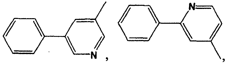
- Organisches Material nach Anspruch 1 oder 2, dadurch gekennzeichnet, dass die mit Ar verbundene Gruppe

- Organisches Material nach Anspruch 1 oder 2, dadurch gekennzeichnet, dass das organische Material repräsentiert wird durch folgende Strukturformeln:


- Verwendung des organischen Materials nach einem der Ansprüche 1 bis 4 als ein Elektronentransportmaterial in einer organischen Elektrolumineszenzvorrichtung.
- Organische Elektrolumineszenzvorrichtung aufweisend ein Paar von Elektroden und ein organisches Lumineszenzmedium, das zwischen dem Paar von Elektroden angeordnet ist, wobei das organische Lumineszenzmedium das organische Material nach einem der Ansprüche 1 bis 4 aufweist.
- Organische Elektrolumineszenzvorrichtung nach Anspruch 6, wobei das organische Lumineszenzmedium eine Lumineszenzschicht und eine Elektronentransport-Funktionsschicht aufweist, wobei das organische Material nach einem der Ansprüche 1 bis 4 in der Elektronentransport-Funktionsschicht enthalten ist.
- Organische Elektrolumineszenzvorrichtung nach Anspruch 7, wobei die Elektronentransport-Funktionsschicht außerdem ein weiteres Elektronentransportmaterial enthält, das ausgewählt ist aus der Gruppe, die aus Oxazol-Verbindungen, Metallchelaten, Triazol-Verbindungen, Imidazol-Verbindungen, Phenanthrolin-Verbindungen oder Anthracen-Verbindungen besteht.
- Organische Elektrolumineszenzvorrichtung nach Anspruch 8, dadurch gekennzeichnet, dass die Oxazol-Verbindungen, Metallchelate, Triazol-Verbindungen, Imidazol-Verbindungen, Phenanthrolin-Vebindungen oder Anthracen-Verbindungen sind:2-(4-Tertbutylphenyl)-5-(4-biphenyl)-1,3,4-oxadiazol,
Tris(8-hydroxychinolato)aluminium,3-(4-Biphenyl)-4-phenyl-5-(4-butylphenyl)-1,2,4-triazol,4,7-Diphenyl-1,10-phenanthrolin, 2,9-Dimethyl-4,7-diphenyl-1,10-phenanthrolin, oder2-Phenyl-9,10-dinaphthylanthracen. - Organische Elektrolumineszenzvorrichtung nach Anspruch 6, wobei das organische Lumineszenzmedium eine Lumineszenzschicht und eine Elektroneninjektions- und Elektronentransport-Funktionsschicht aufweist, wobei das organische Material nach einem der Ansprüche 1 bis 4 in der Elektroneninjektions- und Elektronentransport-Funktionsschicht enthalten ist, und wobei die Elektroneninjektions- und Elektronentransport-Funktionsschicht außerdem ein Dotiermittel enthält, das ausgewählt ist aus der Gruppe, die aus Alkalimetallen, Alkalimetalloxiden, Alkalimetallhalogeniden, Alkalimetallnitriden und Alkalimetallsalzen besteht.
- Organische Elektrolumineszenzvorrichtung nach Anspruch 10, wobei das Dotiermittel ausgewählt ist aus der Gruppe, die besteht aus Lithium, Cäsium, Lithiumnitrid, Lithiumfluorid, Lithiumcobaltat, Lithiumoxid, 8-Hydroxychinolato-lithium, Cäsiumcarbonat, Kaliumborhydrid, Lithiumborhydrid, Natriumfluorid, Natriumchlorid, Cäsiumfluorid, Cäsiumchlorid und Rubidiumoxid.
- Organische Elektrolumineszenzvorrichtung nach Anspruch 10, dadurch gekennzeichnet, dass die Elektroneninjektions- und Elektronentransport-Funktionsschicht eine Dicke von 2 nm bis 40 nm hat und dass der Dotierungsanteil des Dotiermittels in der Elektroneninjektions- und Elektronentransport-Funktionsschicht 0,1 Gew.-% bis 49 Gew.-% auf der Basis des organischen Materials nach einem der Ansprüche 1 bis 4 beträgt.
- Organische Elektrolumineszenzvorrichtung nach Anspruch 12, dadurch gekennzeichnet, dass die Elektroneninjektions- und Elektronentransport-Funktionsschicht eine Dicke von 5 nm bis 25 nm hat und dass der Dotierungsanteil des Dotiermittels in der Elektroneninjektions- und Elektronentransport-Funktionsschicht 0,5 Gew.-% bis 30 Gew.-% auf der Basis des organischen Materials nach einem der Ansprüche 1 bis 4 beträgt.
- Organische Elektrolumineszenzvorrichtung nach Anspruch 10, dadurch gekennzeichnet, dass außerdem eine Pufferschicht zwischen der Elektroneninjektions- und Elektronentransport-Funktionsschicht und der Lumineszenzschicht vorhanden ist, und dass das Material der Pufferschicht aus den Verbindungen, wie sie in Anspruch 1 oder 2 definiert sind, ausgewählt ist oder aus der Gruppe ausgewählt ist, die besteht aus Oxazol-Verbindungen, Metallkomplexen, Triazol-Verbindungen, Imidazol-Verbindungen, Chinolin-Verbindungen, Oxalin-Verbindungen, Phenazin-Verbindungen und Phenanthrolin-Verbindungen.
- Organische Elektrolumineszenzvorrichtung nach Anspruch 14, dadurch gekennzeichnet, dass das Material der Pufferschicht ausgewählt ist aus der Verbindung, wie sie in Anspruch 4 definiert ist, oder ausgewählt ist aus der Gruppe, die besteht aus
2-(4-Tertbutylphenyl)-5-(4-biphenyl)-1,3,4-oxadiazol,
Tris(8-hydroxychinolato)aluminium,
3-(4-Biphenyl)-4-phenyl-5-(4-butylphenyl)-1,2,4-triazol,
4,7-Diphenyl-1,10-phenanthrolin, 2,9-Dimethyl-4,7-diphenyl-1,10-phenanthrolin, und
2-Phenyl-9,10-dinaphthylanthracen. - Organische Elektrolumineszenzvorrichtung nach Anspruch 14, dadurch gekennzeichnet, dass die Pufferschicht eine Dicke von 2 nm bis 20 nm hat.
- Organische Elektrolumineszenzvorrichtung nach Anspruch 6, wobei das organische Lumineszenzmedium mindestens zwei Lumineszenzeinheiten aufweist, wobei zwischen den Lumineszenzeinheiten eine Verbindungsschicht angeordnet ist, wobei das organische Material nach einem der Ansprüche 1 bis 4 in der Verbindungsschicht enthalten ist.
- Organische Elektrolumineszenzvorrichtung nach Anspruch 17, dadurch gekennzeichnet, dass die Verbindungsschicht außerdem dotiert ist mit einem Dotiermittel, das ausgewählt ist aus der Gruppe, die besteht aus Alkalimetallen, Alkalimetalloxiden, Alkalimetallhalogeniden, Alkalimetallnitriden und Alkalimetallsalzen.
- Organische Elektrolumineszenzvorrichtung nach Anspruch 18, dadurch gekennzeichnet, dass das Dotiermittel ausgewählt ist aus der Gruppe, die besteht aus Lithium, Cäsium, Lithiumnitrid, Lithiumfluorid, Lithiumcobaltat, Lithiumoxid, 8-Hydroxychinolato-lithium, Cäsiumcarbonat, Kaliumborhydrid, Lithiumborhydrid, Natriumfluorid, Natriumchlorid, Cäsiumfluorid, Cäsiumchlorid und Rubidiumoxid.
Priority Applications (1)
| Application Number | Priority Date | Filing Date | Title |
|---|---|---|---|
| PL09851216T PL2500343T3 (pl) | 2009-11-13 | 2009-12-30 | Materiały organiczne i stosujące je organiczne urządzenia elektroluminescencyjne |
Applications Claiming Priority (3)
| Application Number | Priority Date | Filing Date | Title |
|---|---|---|---|
| CN 200910234760 CN101891673B (zh) | 2009-11-13 | 2009-11-13 | 一种有机材料及其在有机电致发光器件中的应用 |
| CN 200910234478 CN102074655B (zh) | 2009-11-19 | 2009-11-19 | 一种有机电致发光器件 |
| PCT/CN2009/076276 WO2011057461A1 (zh) | 2009-11-13 | 2009-12-30 | 有机材料及采用该材料的有机电致发光器件 |
Publications (3)
| Publication Number | Publication Date |
|---|---|
| EP2500343A1 EP2500343A1 (de) | 2012-09-19 |
| EP2500343A4 EP2500343A4 (de) | 2013-06-12 |
| EP2500343B1 true EP2500343B1 (de) | 2018-01-31 |
Family
ID=43991181
Family Applications (1)
| Application Number | Title | Priority Date | Filing Date |
|---|---|---|---|
| EP09851216.3A Active EP2500343B1 (de) | 2009-11-13 | 2009-12-30 | Organische materialien und organische elektrolumineszenzvorrichtungen damit |
Country Status (6)
| Country | Link |
|---|---|
| US (1) | US9412951B2 (de) |
| EP (1) | EP2500343B1 (de) |
| JP (1) | JP5498580B2 (de) |
| KR (1) | KR101411122B1 (de) |
| PL (1) | PL2500343T3 (de) |
| WO (1) | WO2011057461A1 (de) |
Families Citing this family (9)
| Publication number | Priority date | Publication date | Assignee | Title |
|---|---|---|---|---|
| JPH1144632A (ja) * | 1997-07-28 | 1999-02-16 | Toa Medical Electronics Co Ltd | 粒子計測装置のデータ異常判定方法 |
| WO2010139175A1 (zh) | 2009-06-05 | 2010-12-09 | 北京维信诺科技有限公司 | 一种有机电致发光器件及其测试方法 |
| CN102795983B (zh) * | 2011-05-25 | 2016-01-20 | 海洋王照明科技股份有限公司 | 蒽醌衍生物材料及其制备方法和应用 |
| CN104025332A (zh) * | 2011-11-28 | 2014-09-03 | 海洋王照明科技股份有限公司 | 掺杂有机电致发光器件及其制备方法 |
| JP6126577B2 (ja) * | 2012-02-28 | 2017-05-10 | 保土谷化学工業株式会社 | 置換基を有するピリジル基とトリフェニレン環構造を有する化合物および有機エレクトロルミネッセンス素子 |
| CN104487432B (zh) | 2012-07-13 | 2018-06-12 | 株式会社Lg化学 | 杂环化合物及包含其的有机电子器件 |
| JP6322587B2 (ja) * | 2013-02-08 | 2018-05-09 | 株式会社Joled | 有機エレクトロルミネッセンス素子 |
| KR102104637B1 (ko) * | 2013-06-28 | 2020-04-27 | 삼성디스플레이 주식회사 | 유기전계발광소자 |
| CN103382181B (zh) * | 2013-07-09 | 2015-05-20 | 京东方科技集团股份有限公司 | 多芳基取代嘧啶衍生物及其制备方法、有机电致发光器件、有机电致发光显示装置 |
Citations (1)
| Publication number | Priority date | Publication date | Assignee | Title |
|---|---|---|---|---|
| US20080111473A1 (en) * | 2004-12-22 | 2008-05-15 | Idemitsu Kosan Co., Ltd. | Anthracene Derivative and Organic Electroluminescent Element Using the Same |
Family Cites Families (57)
| Publication number | Priority date | Publication date | Assignee | Title |
|---|---|---|---|---|
| JPH07159483A (ja) | 1993-12-09 | 1995-06-23 | Toshiba Corp | 集積回路装置およびそのテスト方法 |
| KR0148078B1 (ko) | 1995-07-25 | 1998-08-01 | 김광호 | 연장된 리드를 갖는 리드 온 칩용 리드프레임 |
| JP3541625B2 (ja) | 1997-07-02 | 2004-07-14 | セイコーエプソン株式会社 | 表示装置及びアクティブマトリクス基板 |
| JP2000134411A (ja) | 1998-10-27 | 2000-05-12 | Canon Inc | イメージセンサ及びそれを備えた情報処理装置 |
| JP2000259091A (ja) | 1999-03-04 | 2000-09-22 | Casio Comput Co Ltd | 表示パネル、フレキシブル配線基板及びそれらを備えた表示装置 |
| JP4013503B2 (ja) | 2001-08-24 | 2007-11-28 | セイコーエプソン株式会社 | 電気光学パネルの検査方法 |
| JP4380954B2 (ja) | 2001-09-28 | 2009-12-09 | 三洋電機株式会社 | アクティブマトリクス型表示装置 |
| CN1239447C (zh) | 2002-01-15 | 2006-02-01 | 清华大学 | 一种有机电致发光材料 |
| CN1435893A (zh) | 2002-01-30 | 2003-08-13 | 胜园科技股份有限公司 | 有机发光二极管显示器电极引线的布设结构 |
| JP4054861B2 (ja) | 2002-08-08 | 2008-03-05 | 三菱電機株式会社 | 表示装置および表示装置の製造方法 |
| CN100485995C (zh) | 2002-12-30 | 2009-05-06 | 铼宝科技股份有限公司 | 电激发光显示装置 |
| CN100439978C (zh) | 2003-03-07 | 2008-12-03 | 友达光电股份有限公司 | 液晶显示面板的测试方法及其设备 |
| KR101088103B1 (ko) | 2003-10-28 | 2011-11-29 | 가부시키가이샤 한도오따이 에네루기 켄큐쇼 | 표시장치, 및 텔레비전 수상기 |
| JP4480989B2 (ja) | 2003-11-28 | 2010-06-16 | オプトレックス株式会社 | 有機el表示装置 |
| JP5167571B2 (ja) | 2004-02-18 | 2013-03-21 | ソニー株式会社 | 表示素子 |
| JP2005241988A (ja) | 2004-02-26 | 2005-09-08 | Alps Electric Co Ltd | 表示装置 |
| US7503821B2 (en) | 2004-07-23 | 2009-03-17 | Lg Display Co., Ltd. | Mother glass and method of fabricating organic electro luminescence display device using the same |
| US7247529B2 (en) | 2004-08-30 | 2007-07-24 | Semiconductor Energy Laboratory Co., Ltd. | Method for manufacturing display device |
| KR100588018B1 (ko) | 2004-09-30 | 2006-06-09 | 엘지전자 주식회사 | 모기판 및 이를 이용한 유기전계발광표시소자의 제조방법 |
| KR100632662B1 (ko) | 2005-04-18 | 2006-10-12 | 엘지전자 주식회사 | 유기 전계 발광 패널 |
| TWI259027B (en) | 2005-04-29 | 2006-07-21 | Univision Technology Inc | Organic electroluminescence device capable of preventing long-distance short circuit |
| KR20060120328A (ko) | 2005-05-19 | 2006-11-27 | 엘지.필립스 엘시디 주식회사 | 액정표시장치용 어레이기판 |
| JP4428329B2 (ja) | 2005-05-30 | 2010-03-10 | エプソンイメージングデバイス株式会社 | 電気光学装置及びその製造方法並びに電子機器 |
| CN1889800A (zh) | 2005-06-29 | 2007-01-03 | 铼宝科技股份有限公司 | 有机电激发光显示面板 |
| US7489204B2 (en) | 2005-06-30 | 2009-02-10 | International Business Machines Corporation | Method and structure for chip-level testing of wire delay independent of silicon delay |
| US20070048545A1 (en) * | 2005-08-31 | 2007-03-01 | Eastman Kodak Company | Electron-transporting layer for white OLED device |
| US20070046189A1 (en) * | 2005-08-31 | 2007-03-01 | Eastman Kodak Company | Intermediate connector for a tandem OLED device |
| KR100890862B1 (ko) | 2005-11-07 | 2009-03-27 | 주식회사 엘지화학 | 유기 발광 소자 및 이의 제조 방법 |
| JP2007147949A (ja) | 2005-11-28 | 2007-06-14 | Epson Imaging Devices Corp | 電気光学装置、及び電気光学装置の検査方法、電気光学装置の製造方法、並びに電子機器 |
| TW200729129A (en) | 2006-01-17 | 2007-08-01 | Chi Mei El Corp | Flat panel display and its testing method |
| KR100736575B1 (ko) | 2006-04-28 | 2007-07-06 | 엘지전자 주식회사 | 디스플레이 소자용 모기판 및 이를 이용한 디스플레이 장치 |
| CN101077971B (zh) | 2006-05-25 | 2010-08-11 | 清华大学 | 一种有机电致磷光发光材料及其应用 |
| KR100903203B1 (ko) * | 2006-11-30 | 2009-06-18 | 에스에프씨 주식회사 | 안트라센 유도체 및 이를 채용한 유기전계발광소자 |
| JP2008162921A (ja) | 2006-12-27 | 2008-07-17 | Idemitsu Kosan Co Ltd | ベンゾチアジアゾール誘導体及びそれを用いた有機エレクトロルミネッセンス素子用 |
| CN101221971A (zh) | 2007-01-11 | 2008-07-16 | 奇晶光电股份有限公司 | 平面显示器及该平面显示器的测试方法 |
| DE102007029663B3 (de) | 2007-06-27 | 2008-11-20 | Alfing Kessler Sondermaschinen Gmbh | Bruchtrennmodul für eine Werkzeugmaschine, Werkzeugmaschine mit einem Bruchtrennmodul und Verfahren zum Bruchtrennen |
| JP2010245060A (ja) * | 2007-07-07 | 2010-10-28 | Idemitsu Kosan Co Ltd | 有機el素子 |
| CN101188247B (zh) | 2007-08-16 | 2010-11-10 | 清华大学 | 一种有机电致发光显示器及其制备方法 |
| KR100961781B1 (ko) * | 2007-09-17 | 2010-06-07 | 에스에프씨 주식회사 | n형 유기반도체 화합물 및 이를 이용한 유기전계발광소자 |
| CN101412907A (zh) | 2007-10-17 | 2009-04-22 | 中国科学院理化技术研究所 | 有机电致发光材料及其合成方法和用途 |
| KR100911962B1 (ko) | 2007-10-22 | 2009-08-13 | 삼성모바일디스플레이주식회사 | 유기전계발광 표시 장치 |
| WO2009054253A1 (ja) * | 2007-10-26 | 2009-04-30 | Konica Minolta Holdings, Inc. | 有機エレクトロルミネッセンス素子、表示装置及び照明装置 |
| JP5353233B2 (ja) | 2007-12-27 | 2013-11-27 | Jnc株式会社 | ピリジルフェニル基を有するアントラセン誘導体化合物及び有機電界発光素子 |
| US7955719B2 (en) * | 2008-01-30 | 2011-06-07 | Global Oled Technology Llc | Tandem OLED device with intermediate connector |
| KR101068224B1 (ko) * | 2008-02-05 | 2011-09-28 | 에스에프씨 주식회사 | 안트라센 유도체 및 이를 포함하는 유기전계발광소자 |
| JP5304010B2 (ja) | 2008-04-23 | 2013-10-02 | コニカミノルタ株式会社 | 有機エレクトロルミネッセンス素子、表示装置及び照明装置 |
| KR20090111915A (ko) * | 2008-04-23 | 2009-10-28 | (주)그라쎌 | 신규한 유기 발광 화합물 및 이를 발광재료로서 채용하고있는 유기 발광 소자 |
| WO2009136596A1 (ja) | 2008-05-08 | 2009-11-12 | 新日鐵化学株式会社 | 有機電界発光素子 |
| CN101407493B (zh) * | 2008-05-29 | 2010-07-21 | 清华大学 | 一种有机材料及其在有机电致发光器件中的应用 |
| CN101308749A (zh) | 2008-06-06 | 2008-11-19 | 南京华显高科有限公司 | 等离子体显示器用实验测试屏 |
| EP2256176A1 (de) | 2008-06-25 | 2010-12-01 | Gracel Display Inc. | Neue organische Elektrolumineszenzverbindungen und organische Elektrolumineszenzvorrichtung damit |
| KR101551207B1 (ko) * | 2008-09-04 | 2015-09-08 | 롬엔드하스전자재료코리아유한회사 | 신규한 유기 발광 화합물 및 이를 발광재료로서 채용하고 있는 유기 발광 소자 |
| CN101364636A (zh) | 2008-09-28 | 2009-02-11 | 清华大学 | 一种有机电致发光器件 |
| KR101507166B1 (ko) | 2008-12-08 | 2015-04-30 | 엘지디스플레이 주식회사 | 청색 발광 화합물 및 이를 포함하는 유기전계발광소자 |
| CN101452997B (zh) * | 2008-12-31 | 2011-06-22 | 清华大学 | 一种叠层结构有机电致发光器件 |
| WO2010139175A1 (zh) | 2009-06-05 | 2010-12-09 | 北京维信诺科技有限公司 | 一种有机电致发光器件及其测试方法 |
| CN102074655B (zh) | 2009-11-19 | 2013-05-01 | 昆山维信诺显示技术有限公司 | 一种有机电致发光器件 |
-
2009
- 2009-12-30 WO PCT/CN2009/076276 patent/WO2011057461A1/zh not_active Ceased
- 2009-12-30 EP EP09851216.3A patent/EP2500343B1/de active Active
- 2009-12-30 PL PL09851216T patent/PL2500343T3/pl unknown
- 2009-12-30 JP JP2012527175A patent/JP5498580B2/ja active Active
- 2009-12-30 KR KR1020127004954A patent/KR101411122B1/ko active Active
- 2009-12-30 US US13/497,131 patent/US9412951B2/en active Active
Patent Citations (1)
| Publication number | Priority date | Publication date | Assignee | Title |
|---|---|---|---|---|
| US20080111473A1 (en) * | 2004-12-22 | 2008-05-15 | Idemitsu Kosan Co., Ltd. | Anthracene Derivative and Organic Electroluminescent Element Using the Same |
Also Published As
| Publication number | Publication date |
|---|---|
| WO2011057461A1 (zh) | 2011-05-19 |
| KR20120067999A (ko) | 2012-06-26 |
| KR101411122B1 (ko) | 2014-06-25 |
| US20130087771A1 (en) | 2013-04-11 |
| US9412951B2 (en) | 2016-08-09 |
| EP2500343A1 (de) | 2012-09-19 |
| PL2500343T3 (pl) | 2018-08-31 |
| JP2013503497A (ja) | 2013-01-31 |
| JP5498580B2 (ja) | 2014-05-21 |
| EP2500343A4 (de) | 2013-06-12 |
Similar Documents
| Publication | Publication Date | Title |
|---|---|---|
| EP2338186B1 (de) | Organisches leuchtbauelement und materialien zur verwendung darin | |
| EP2660300B1 (de) | Neue verbindung und organische lichtemittierende vorrichtung damit | |
| US9412951B2 (en) | Organic materials and organic electroluminescent apparatuses using the same | |
| EP2431445B1 (de) | Verbindung für organische photoelektrische vorrichtung und organische photoelektrische vorrichtung damit | |
| EP1501821B1 (de) | Neue organische verbindungen für die elektrolumineszenz und organisch-elektrolumineszente vorrichtungen, in denen diese verbindungen verwendet werden | |
| EP2277978B1 (de) | Triphenylen wirtsmaterialien in phosphoreszierenden lichtemittierenden dioden. | |
| CN1625552B (zh) | 电子传输新材料和使用该材料的有机电致发光显示器 | |
| EP2476738B1 (de) | Neues heterozyklisches derivat und organische lichtemittierende vorrichtung damit | |
| CN102282695B (zh) | 有机电致发光元件 | |
| TWI459857B (zh) | 含有熒蒽電子傳遞材料之有機發光二極體(oled)裝置 | |
| EP2139846B1 (de) | Neue diaminderivate und diese verwendende organische elektronische vorrichtung | |
| US20060222886A1 (en) | Arylpyrene compounds | |
| US20050025993A1 (en) | Materials and structures for enhancing the performance of organic light emitting devices | |
| Wang et al. | Highly efficient red thermally activated delayed fluorescence materials based on a cyano-containing planar acceptor | |
| TW201038576A (en) | Materials for organic electroluminescent devices | |
| EP2378585A1 (de) | Material für ein organisches elektrolumineszenzelement und organisches elektrolumineszenzelement damit | |
| EP3527564B1 (de) | Neuartige heterocyclische verbindung und organisches lichtemittierendes element mit verwendung davon | |
| CN101364636A (zh) | 一种有机电致发光器件 | |
| KR20190025788A (ko) | 벤즈아졸 유도체를 리간드로 하는 유기 금속 착물 및 이를 포함한 유기 전계발광 소자 | |
| WO2025218088A1 (zh) | 化合物、电致发光器件及显示面板 | |
| Xia et al. | Efficient blue fluorescent OLEDs based on a D–π–A emitter with the hybridized localized and charge-transfer state | |
| EP2372804A1 (de) | Organisches elektrolumineszenzelement und verbindung | |
| EP1880990A1 (de) | Neues organisches elektrolumineszierendes material, organisches elektrolumineszierendes element, bei dem dieses verwendet wird, und eine einen dünnen film bildende lösung für organische elektrolumineszenz | |
| Krucaite et al. | Tetramer of triphenylamine and similar derivatives with bromine atoms as hole injecting/transporting materials for efficient red phosphorescent OLEDs | |
| CN106008498A (zh) | 啡啉衍生物及使用其的有机电激发光装置 |
Legal Events
| Date | Code | Title | Description |
|---|---|---|---|
| PUAI | Public reference made under article 153(3) epc to a published international application that has entered the european phase |
Free format text: ORIGINAL CODE: 0009012 |
|
| 17P | Request for examination filed |
Effective date: 20120223 |
|
| AK | Designated contracting states |
Kind code of ref document: A1 Designated state(s): AT BE BG CH CY CZ DE DK EE ES FI FR GB GR HR HU IE IS IT LI LT LU LV MC MK MT NL NO PL PT RO SE SI SK SM TR |
|
| DAX | Request for extension of the european patent (deleted) | ||
| RIC1 | Information provided on ipc code assigned before grant |
Ipc: C09K 11/06 20060101AFI20130426BHEP Ipc: H01L 51/54 20060101ALI20130426BHEP Ipc: H01L 51/50 20060101ALI20130426BHEP Ipc: C07D 213/53 20060101ALI20130426BHEP |
|
| A4 | Supplementary search report drawn up and despatched |
Effective date: 20130514 |
|
| 17Q | First examination report despatched |
Effective date: 20160401 |
|
| REG | Reference to a national code |
Ref country code: DE Ref legal event code: R079 Ref document number: 602009050652 Country of ref document: DE Free format text: PREVIOUS MAIN CLASS: C07D0401100000 Ipc: C09K0011060000 |
|
| GRAP | Despatch of communication of intention to grant a patent |
Free format text: ORIGINAL CODE: EPIDOSNIGR1 |
|
| STAA | Information on the status of an ep patent application or granted ep patent |
Free format text: STATUS: GRANT OF PATENT IS INTENDED |
|
| RIC1 | Information provided on ipc code assigned before grant |
Ipc: C07D 213/53 20060101ALI20170615BHEP Ipc: H05B 33/14 20060101ALI20170615BHEP Ipc: H01L 51/00 20060101ALI20170615BHEP Ipc: H01L 51/54 20060101ALI20170615BHEP Ipc: H01L 51/50 20060101ALI20170615BHEP Ipc: C09K 11/06 20060101AFI20170615BHEP |
|
| INTG | Intention to grant announced |
Effective date: 20170712 |
|
| GRAS | Grant fee paid |
Free format text: ORIGINAL CODE: EPIDOSNIGR3 |
|
| GRAA | (expected) grant |
Free format text: ORIGINAL CODE: 0009210 |
|
| STAA | Information on the status of an ep patent application or granted ep patent |
Free format text: STATUS: THE PATENT HAS BEEN GRANTED |
|
| AK | Designated contracting states |
Kind code of ref document: B1 Designated state(s): AT BE BG CH CY CZ DE DK EE ES FI FR GB GR HR HU IE IS IT LI LT LU LV MC MK MT NL NO PL PT RO SE SI SK SM TR |
|
| REG | Reference to a national code |
Ref country code: GB Ref legal event code: FG4D Ref country code: CH Ref legal event code: EP |
|
| REG | Reference to a national code |
Ref country code: AT Ref legal event code: REF Ref document number: 967378 Country of ref document: AT Kind code of ref document: T Effective date: 20180215 |
|
| REG | Reference to a national code |
Ref country code: IE Ref legal event code: FG4D |
|
| REG | Reference to a national code |
Ref country code: DE Ref legal event code: R096 Ref document number: 602009050652 Country of ref document: DE |
|
| REG | Reference to a national code |
Ref country code: NL Ref legal event code: FP |
|
| REG | Reference to a national code |
Ref country code: CH Ref legal event code: NV Representative=s name: PATENTANWAELTE SCHAAD, BALASS, MENZL AND PARTN, CH |
|
| REG | Reference to a national code |
Ref country code: LT Ref legal event code: MG4D |
|
| REG | Reference to a national code |
Ref country code: AT Ref legal event code: MK05 Ref document number: 967378 Country of ref document: AT Kind code of ref document: T Effective date: 20180131 |
|
| PG25 | Lapsed in a contracting state [announced via postgrant information from national office to epo] |
Ref country code: LT Free format text: LAPSE BECAUSE OF FAILURE TO SUBMIT A TRANSLATION OF THE DESCRIPTION OR TO PAY THE FEE WITHIN THE PRESCRIBED TIME-LIMIT Effective date: 20180131 Ref country code: NO Free format text: LAPSE BECAUSE OF FAILURE TO SUBMIT A TRANSLATION OF THE DESCRIPTION OR TO PAY THE FEE WITHIN THE PRESCRIBED TIME-LIMIT Effective date: 20180430 Ref country code: ES Free format text: LAPSE BECAUSE OF FAILURE TO SUBMIT A TRANSLATION OF THE DESCRIPTION OR TO PAY THE FEE WITHIN THE PRESCRIBED TIME-LIMIT Effective date: 20180131 Ref country code: HR Free format text: LAPSE BECAUSE OF FAILURE TO SUBMIT A TRANSLATION OF THE DESCRIPTION OR TO PAY THE FEE WITHIN THE PRESCRIBED TIME-LIMIT Effective date: 20180131 |
|
| PG25 | Lapsed in a contracting state [announced via postgrant information from national office to epo] |
Ref country code: GR Free format text: LAPSE BECAUSE OF FAILURE TO SUBMIT A TRANSLATION OF THE DESCRIPTION OR TO PAY THE FEE WITHIN THE PRESCRIBED TIME-LIMIT Effective date: 20180501 Ref country code: BG Free format text: LAPSE BECAUSE OF FAILURE TO SUBMIT A TRANSLATION OF THE DESCRIPTION OR TO PAY THE FEE WITHIN THE PRESCRIBED TIME-LIMIT Effective date: 20180430 Ref country code: AT Free format text: LAPSE BECAUSE OF FAILURE TO SUBMIT A TRANSLATION OF THE DESCRIPTION OR TO PAY THE FEE WITHIN THE PRESCRIBED TIME-LIMIT Effective date: 20180131 Ref country code: IS Free format text: LAPSE BECAUSE OF FAILURE TO SUBMIT A TRANSLATION OF THE DESCRIPTION OR TO PAY THE FEE WITHIN THE PRESCRIBED TIME-LIMIT Effective date: 20180531 Ref country code: SE Free format text: LAPSE BECAUSE OF FAILURE TO SUBMIT A TRANSLATION OF THE DESCRIPTION OR TO PAY THE FEE WITHIN THE PRESCRIBED TIME-LIMIT Effective date: 20180131 Ref country code: LV Free format text: LAPSE BECAUSE OF FAILURE TO SUBMIT A TRANSLATION OF THE DESCRIPTION OR TO PAY THE FEE WITHIN THE PRESCRIBED TIME-LIMIT Effective date: 20180131 |
|
| PG25 | Lapsed in a contracting state [announced via postgrant information from national office to epo] |
Ref country code: RO Free format text: LAPSE BECAUSE OF FAILURE TO SUBMIT A TRANSLATION OF THE DESCRIPTION OR TO PAY THE FEE WITHIN THE PRESCRIBED TIME-LIMIT Effective date: 20180131 Ref country code: EE Free format text: LAPSE BECAUSE OF FAILURE TO SUBMIT A TRANSLATION OF THE DESCRIPTION OR TO PAY THE FEE WITHIN THE PRESCRIBED TIME-LIMIT Effective date: 20180131 |
|
| REG | Reference to a national code |
Ref country code: DE Ref legal event code: R097 Ref document number: 602009050652 Country of ref document: DE |
|
| PG25 | Lapsed in a contracting state [announced via postgrant information from national office to epo] |
Ref country code: CZ Free format text: LAPSE BECAUSE OF FAILURE TO SUBMIT A TRANSLATION OF THE DESCRIPTION OR TO PAY THE FEE WITHIN THE PRESCRIBED TIME-LIMIT Effective date: 20180131 Ref country code: SM Free format text: LAPSE BECAUSE OF FAILURE TO SUBMIT A TRANSLATION OF THE DESCRIPTION OR TO PAY THE FEE WITHIN THE PRESCRIBED TIME-LIMIT Effective date: 20180131 Ref country code: DK Free format text: LAPSE BECAUSE OF FAILURE TO SUBMIT A TRANSLATION OF THE DESCRIPTION OR TO PAY THE FEE WITHIN THE PRESCRIBED TIME-LIMIT Effective date: 20180131 Ref country code: SK Free format text: LAPSE BECAUSE OF FAILURE TO SUBMIT A TRANSLATION OF THE DESCRIPTION OR TO PAY THE FEE WITHIN THE PRESCRIBED TIME-LIMIT Effective date: 20180131 |
|
| PLBE | No opposition filed within time limit |
Free format text: ORIGINAL CODE: 0009261 |
|
| STAA | Information on the status of an ep patent application or granted ep patent |
Free format text: STATUS: NO OPPOSITION FILED WITHIN TIME LIMIT |
|
| 26N | No opposition filed |
Effective date: 20181102 |
|
| PG25 | Lapsed in a contracting state [announced via postgrant information from national office to epo] |
Ref country code: SI Free format text: LAPSE BECAUSE OF FAILURE TO SUBMIT A TRANSLATION OF THE DESCRIPTION OR TO PAY THE FEE WITHIN THE PRESCRIBED TIME-LIMIT Effective date: 20180131 |
|
| PG25 | Lapsed in a contracting state [announced via postgrant information from national office to epo] |
Ref country code: LU Free format text: LAPSE BECAUSE OF NON-PAYMENT OF DUE FEES Effective date: 20181230 Ref country code: MC Free format text: LAPSE BECAUSE OF FAILURE TO SUBMIT A TRANSLATION OF THE DESCRIPTION OR TO PAY THE FEE WITHIN THE PRESCRIBED TIME-LIMIT Effective date: 20180131 |
|
| REG | Reference to a national code |
Ref country code: IE Ref legal event code: MM4A |
|
| REG | Reference to a national code |
Ref country code: BE Ref legal event code: MM Effective date: 20181231 |
|
| PG25 | Lapsed in a contracting state [announced via postgrant information from national office to epo] |
Ref country code: IE Free format text: LAPSE BECAUSE OF NON-PAYMENT OF DUE FEES Effective date: 20181230 |
|
| PG25 | Lapsed in a contracting state [announced via postgrant information from national office to epo] |
Ref country code: BE Free format text: LAPSE BECAUSE OF NON-PAYMENT OF DUE FEES Effective date: 20181231 |
|
| PG25 | Lapsed in a contracting state [announced via postgrant information from national office to epo] |
Ref country code: MT Free format text: LAPSE BECAUSE OF NON-PAYMENT OF DUE FEES Effective date: 20181230 |
|
| PG25 | Lapsed in a contracting state [announced via postgrant information from national office to epo] |
Ref country code: TR Free format text: LAPSE BECAUSE OF FAILURE TO SUBMIT A TRANSLATION OF THE DESCRIPTION OR TO PAY THE FEE WITHIN THE PRESCRIBED TIME-LIMIT Effective date: 20180131 |
|
| PG25 | Lapsed in a contracting state [announced via postgrant information from national office to epo] |
Ref country code: PT Free format text: LAPSE BECAUSE OF FAILURE TO SUBMIT A TRANSLATION OF THE DESCRIPTION OR TO PAY THE FEE WITHIN THE PRESCRIBED TIME-LIMIT Effective date: 20180131 |
|
| PG25 | Lapsed in a contracting state [announced via postgrant information from national office to epo] |
Ref country code: CY Free format text: LAPSE BECAUSE OF FAILURE TO SUBMIT A TRANSLATION OF THE DESCRIPTION OR TO PAY THE FEE WITHIN THE PRESCRIBED TIME-LIMIT Effective date: 20180131 Ref country code: HU Free format text: LAPSE BECAUSE OF FAILURE TO SUBMIT A TRANSLATION OF THE DESCRIPTION OR TO PAY THE FEE WITHIN THE PRESCRIBED TIME-LIMIT; INVALID AB INITIO Effective date: 20091230 Ref country code: MK Free format text: LAPSE BECAUSE OF NON-PAYMENT OF DUE FEES Effective date: 20180131 |
|
| P01 | Opt-out of the competence of the unified patent court (upc) registered |
Effective date: 20230526 |
|
| PGFP | Annual fee paid to national office [announced via postgrant information from national office to epo] |
Ref country code: NL Payment date: 20251127 Year of fee payment: 17 |
|
| REG | Reference to a national code |
Ref country code: CH Ref legal event code: U11 Free format text: ST27 STATUS EVENT CODE: U-0-0-U10-U11 (AS PROVIDED BY THE NATIONAL OFFICE) Effective date: 20260101 |
|
| PGFP | Annual fee paid to national office [announced via postgrant information from national office to epo] |
Ref country code: GB Payment date: 20251229 Year of fee payment: 17 |
|
| PGFP | Annual fee paid to national office [announced via postgrant information from national office to epo] |
Ref country code: IT Payment date: 20251209 Year of fee payment: 17 Ref country code: FI Payment date: 20251124 Year of fee payment: 17 |
|
| PGFP | Annual fee paid to national office [announced via postgrant information from national office to epo] |
Ref country code: FR Payment date: 20251230 Year of fee payment: 17 |
|
| PGFP | Annual fee paid to national office [announced via postgrant information from national office to epo] |
Ref country code: PL Payment date: 20251125 Year of fee payment: 17 |
|
| PGFP | Annual fee paid to national office [announced via postgrant information from national office to epo] |
Ref country code: DE Payment date: 20251231 Year of fee payment: 17 |
|
| PGFP | Annual fee paid to national office [announced via postgrant information from national office to epo] |
Ref country code: CH Payment date: 20260101 Year of fee payment: 17 |