EP1501821B1 - Neue organische verbindungen für die elektrolumineszenz und organisch-elektrolumineszente vorrichtungen, in denen diese verbindungen verwendet werden - Google Patents
Neue organische verbindungen für die elektrolumineszenz und organisch-elektrolumineszente vorrichtungen, in denen diese verbindungen verwendet werden Download PDFInfo
- Publication number
- EP1501821B1 EP1501821B1 EP03723417.6A EP03723417A EP1501821B1 EP 1501821 B1 EP1501821 B1 EP 1501821B1 EP 03723417 A EP03723417 A EP 03723417A EP 1501821 B1 EP1501821 B1 EP 1501821B1
- Authority
- EP
- European Patent Office
- Prior art keywords
- compound
- light
- organic
- compounds
- emitting
- Prior art date
- Legal status (The legal status is an assumption and is not a legal conclusion. Google has not performed a legal analysis and makes no representation as to the accuracy of the status listed.)
- Expired - Lifetime
Links
- 0 CC1C(C(CCC2)=C)*2=CC(C)C1 Chemical compound CC1C(C(CCC2)=C)*2=CC(C)C1 0.000 description 9
- MSDMPJCOOXURQD-UHFFFAOYSA-N CC(C)(CCN1c2c3C(C)(C)CC1)c2cc(C=C1c2nc(cccc4)c4[s]2)c3OC1=O Chemical compound CC(C)(CCN1c2c3C(C)(C)CC1)c2cc(C=C1c2nc(cccc4)c4[s]2)c3OC1=O MSDMPJCOOXURQD-UHFFFAOYSA-N 0.000 description 2
- VBVAVBCYMYWNOU-UHFFFAOYSA-N CCN(CC)c1ccc(C=C(c2nc(cccc3)c3[s]2)C(O2)=O)c2c1 Chemical compound CCN(CC)c1ccc(C=C(c2nc(cccc3)c3[s]2)C(O2)=O)c2c1 VBVAVBCYMYWNOU-UHFFFAOYSA-N 0.000 description 2
- NNCVEIRPVYCFQX-UHFFFAOYSA-N c1c(-c2ccc(-c(cc3)c(cc(cccc4)c4c4)c4c3-c3ccc(-c4ccc(-c5cc6c(-c7cc8ccccc8cc7)c(cccc7)c7c(-c7cc8ccccc8cc7)c6cc5)[s]4)[s]3)[s]2)[s]c(-c2cc3c(-c4cc5ccccc5cc4)c(cccc4)c4c(-c4cc(cccc5)c5cc4)c3cc2)c1 Chemical compound c1c(-c2ccc(-c(cc3)c(cc(cccc4)c4c4)c4c3-c3ccc(-c4ccc(-c5cc6c(-c7cc8ccccc8cc7)c(cccc7)c7c(-c7cc8ccccc8cc7)c6cc5)[s]4)[s]3)[s]2)[s]c(-c2cc3c(-c4cc5ccccc5cc4)c(cccc4)c4c(-c4cc(cccc5)c5cc4)c3cc2)c1 NNCVEIRPVYCFQX-UHFFFAOYSA-N 0.000 description 2
- CFZAFKWGMOXOHG-BQYQJAHWSA-N CC(C)(C(OC(/C=C/c(cc1C(C)(C)CC2)cc3c1N2CCC3(C)C)=C1)=CC1=C(C#N)C#N)I Chemical compound CC(C)(C(OC(/C=C/c(cc1C(C)(C)CC2)cc3c1N2CCC3(C)C)=C1)=CC1=C(C#N)C#N)I CFZAFKWGMOXOHG-BQYQJAHWSA-N 0.000 description 1
- XDADCUUORAKGEF-UHFFFAOYSA-N Cc1c(cccc2)c2c(C)c2c1ccc(-c1ccc(-c3ccc(-c4c(cccc5)c5ccc4)[s]3)[s]1)c2 Chemical compound Cc1c(cccc2)c2c(C)c2c1ccc(-c1ccc(-c3ccc(-c4c(cccc5)c5ccc4)[s]3)[s]1)c2 XDADCUUORAKGEF-UHFFFAOYSA-N 0.000 description 1
- RLRJNQFXMVRXPJ-UHFFFAOYSA-N N#CC(C#N)=Cc1ccc(-c2ccc(-c(cc3)cc4c3c(-c3ccc(cccc5)c5c3)c(cccc3)c3c4-c3cc(cccc4)c4cc3)[s]2)[s]1 Chemical compound N#CC(C#N)=Cc1ccc(-c2ccc(-c(cc3)cc4c3c(-c3ccc(cccc5)c5c3)c(cccc3)c3c4-c3cc(cccc4)c4cc3)[s]2)[s]1 RLRJNQFXMVRXPJ-UHFFFAOYSA-N 0.000 description 1
- AAMZSQQNLGAWLC-UHFFFAOYSA-N NN(C(C1C2)=CC3=C2Nc(c2ccccc2cc2)c2C3=O)c(c(cccc2)c2cc2)c2C1=O Chemical compound NN(C(C1C2)=CC3=C2Nc(c2ccccc2cc2)c2C3=O)c(c(cccc2)c2cc2)c2C1=O AAMZSQQNLGAWLC-UHFFFAOYSA-N 0.000 description 1
- BRRYGOLATSLUES-UHFFFAOYSA-N O=C(c1ccc(cccc2)c2c1Nc1c2)c1cc(Nc1c(cccc3)c3ccc11)c2C1=O Chemical compound O=C(c1ccc(cccc2)c2c1Nc1c2)c1cc(Nc1c(cccc3)c3ccc11)c2C1=O BRRYGOLATSLUES-UHFFFAOYSA-N 0.000 description 1
- NRCMAYZCPIVABH-UHFFFAOYSA-N O=C(c1ccccc1Nc1c2)c1cc(Nc1ccccc11)c2C1=O Chemical compound O=C(c1ccccc1Nc1c2)c1cc(Nc1ccccc11)c2C1=O NRCMAYZCPIVABH-UHFFFAOYSA-N 0.000 description 1
- LTSHKFHTBJUMLW-UHFFFAOYSA-N c1c(-c2ccc(-c(cc3)cc4c3c(-c3cc(cccc5)c5cc3)c(cccc3)c3c4-c3cc(cccc4)c4cc3)[s]2)[s]c(-c2ccccc2)c1 Chemical compound c1c(-c2ccc(-c(cc3)cc4c3c(-c3cc(cccc5)c5cc3)c(cccc3)c3c4-c3cc(cccc4)c4cc3)[s]2)[s]c(-c2ccccc2)c1 LTSHKFHTBJUMLW-UHFFFAOYSA-N 0.000 description 1
- WDIWABKCDJBZQM-UHFFFAOYSA-N c1c(-c2ccc(-c3cc4c(-c5cc6ccccc6cc5)c(cccc5)c5c(-c5cc6ccccc6cc5)c4cc3)[s]2)[s]c(-c(cc2)ccc2N(c2ccccc2)c2ccccc2)c1 Chemical compound c1c(-c2ccc(-c3cc4c(-c5cc6ccccc6cc5)c(cccc5)c5c(-c5cc6ccccc6cc5)c4cc3)[s]2)[s]c(-c(cc2)ccc2N(c2ccccc2)c2ccccc2)c1 WDIWABKCDJBZQM-UHFFFAOYSA-N 0.000 description 1
- OJCKCQQIKRKXFQ-UHFFFAOYSA-N c1c(-c2ccc(N(c3ccccc3)c3ccccc3)[s]2)[s]c(-c(cc2)cc3c2c(-c2ccc(cccc4)c4c2)c(cccc2)c2c3-c2cc3ccccc3cc2)c1 Chemical compound c1c(-c2ccc(N(c3ccccc3)c3ccccc3)[s]2)[s]c(-c(cc2)cc3c2c(-c2ccc(cccc4)c4c2)c(cccc2)c2c3-c2cc3ccccc3cc2)c1 OJCKCQQIKRKXFQ-UHFFFAOYSA-N 0.000 description 1
Images


Classifications
-
- C—CHEMISTRY; METALLURGY
- C09—DYES; PAINTS; POLISHES; NATURAL RESINS; ADHESIVES; COMPOSITIONS NOT OTHERWISE PROVIDED FOR; APPLICATIONS OF MATERIALS NOT OTHERWISE PROVIDED FOR
- C09K—MATERIALS FOR MISCELLANEOUS APPLICATIONS, NOT PROVIDED FOR ELSEWHERE
- C09K11/00—Luminescent materials, e.g. electroluminescent or chemiluminescent
- C09K11/06—Luminescent materials, e.g. electroluminescent or chemiluminescent containing organic luminescent materials
-
- C—CHEMISTRY; METALLURGY
- C07—ORGANIC CHEMISTRY
- C07D—HETEROCYCLIC COMPOUNDS
- C07D333/00—Heterocyclic compounds containing five-membered rings having one sulfur atom as the only ring hetero atom
- C07D333/02—Heterocyclic compounds containing five-membered rings having one sulfur atom as the only ring hetero atom not condensed with other rings
- C07D333/04—Heterocyclic compounds containing five-membered rings having one sulfur atom as the only ring hetero atom not condensed with other rings not substituted on the ring sulphur atom
- C07D333/06—Heterocyclic compounds containing five-membered rings having one sulfur atom as the only ring hetero atom not condensed with other rings not substituted on the ring sulphur atom with only hydrogen atoms, hydrocarbon or substituted hydrocarbon radicals, directly attached to the ring carbon atoms
- C07D333/08—Hydrogen atoms or radicals containing only hydrogen and carbon atoms
-
- C—CHEMISTRY; METALLURGY
- C07—ORGANIC CHEMISTRY
- C07D—HETEROCYCLIC COMPOUNDS
- C07D333/00—Heterocyclic compounds containing five-membered rings having one sulfur atom as the only ring hetero atom
- C07D333/02—Heterocyclic compounds containing five-membered rings having one sulfur atom as the only ring hetero atom not condensed with other rings
- C07D333/04—Heterocyclic compounds containing five-membered rings having one sulfur atom as the only ring hetero atom not condensed with other rings not substituted on the ring sulphur atom
- C07D333/06—Heterocyclic compounds containing five-membered rings having one sulfur atom as the only ring hetero atom not condensed with other rings not substituted on the ring sulphur atom with only hydrogen atoms, hydrocarbon or substituted hydrocarbon radicals, directly attached to the ring carbon atoms
- C07D333/14—Radicals substituted by singly bound hetero atoms other than halogen
- C07D333/20—Radicals substituted by singly bound hetero atoms other than halogen by nitrogen atoms
-
- C—CHEMISTRY; METALLURGY
- C07—ORGANIC CHEMISTRY
- C07D—HETEROCYCLIC COMPOUNDS
- C07D333/00—Heterocyclic compounds containing five-membered rings having one sulfur atom as the only ring hetero atom
- C07D333/02—Heterocyclic compounds containing five-membered rings having one sulfur atom as the only ring hetero atom not condensed with other rings
- C07D333/04—Heterocyclic compounds containing five-membered rings having one sulfur atom as the only ring hetero atom not condensed with other rings not substituted on the ring sulphur atom
- C07D333/06—Heterocyclic compounds containing five-membered rings having one sulfur atom as the only ring hetero atom not condensed with other rings not substituted on the ring sulphur atom with only hydrogen atoms, hydrocarbon or substituted hydrocarbon radicals, directly attached to the ring carbon atoms
- C07D333/24—Radicals substituted by carbon atoms having three bonds to hetero atoms with at the most one bond to halogen, e.g. ester or nitrile radicals
-
- C—CHEMISTRY; METALLURGY
- C07—ORGANIC CHEMISTRY
- C07D—HETEROCYCLIC COMPOUNDS
- C07D333/00—Heterocyclic compounds containing five-membered rings having one sulfur atom as the only ring hetero atom
- C07D333/02—Heterocyclic compounds containing five-membered rings having one sulfur atom as the only ring hetero atom not condensed with other rings
- C07D333/04—Heterocyclic compounds containing five-membered rings having one sulfur atom as the only ring hetero atom not condensed with other rings not substituted on the ring sulphur atom
- C07D333/26—Heterocyclic compounds containing five-membered rings having one sulfur atom as the only ring hetero atom not condensed with other rings not substituted on the ring sulphur atom with hetero atoms or with carbon atoms having three bonds to hetero atoms with at the most one bond to halogen, e.g. ester or nitrile radicals, directly attached to ring carbon atoms
- C07D333/30—Hetero atoms other than halogen
- C07D333/36—Nitrogen atoms
-
- C—CHEMISTRY; METALLURGY
- C07—ORGANIC CHEMISTRY
- C07D—HETEROCYCLIC COMPOUNDS
- C07D409/00—Heterocyclic compounds containing two or more hetero rings, at least one ring having sulfur atoms as the only ring hetero atoms
- C07D409/14—Heterocyclic compounds containing two or more hetero rings, at least one ring having sulfur atoms as the only ring hetero atoms containing three or more hetero rings
-
- C—CHEMISTRY; METALLURGY
- C07—ORGANIC CHEMISTRY
- C07D—HETEROCYCLIC COMPOUNDS
- C07D413/00—Heterocyclic compounds containing two or more hetero rings, at least one ring having nitrogen and oxygen atoms as the only ring hetero atoms
- C07D413/14—Heterocyclic compounds containing two or more hetero rings, at least one ring having nitrogen and oxygen atoms as the only ring hetero atoms containing three or more hetero rings
-
- C—CHEMISTRY; METALLURGY
- C07—ORGANIC CHEMISTRY
- C07D—HETEROCYCLIC COMPOUNDS
- C07D417/00—Heterocyclic compounds containing two or more hetero rings, at least one ring having nitrogen and sulfur atoms as the only ring hetero atoms, not provided for by group C07D415/00
- C07D417/14—Heterocyclic compounds containing two or more hetero rings, at least one ring having nitrogen and sulfur atoms as the only ring hetero atoms, not provided for by group C07D415/00 containing three or more hetero rings
-
- C—CHEMISTRY; METALLURGY
- C09—DYES; PAINTS; POLISHES; NATURAL RESINS; ADHESIVES; COMPOSITIONS NOT OTHERWISE PROVIDED FOR; APPLICATIONS OF MATERIALS NOT OTHERWISE PROVIDED FOR
- C09B—ORGANIC DYES OR CLOSELY-RELATED COMPOUNDS FOR PRODUCING DYES, e.g. PIGMENTS; MORDANTS; LAKES
- C09B1/00—Dyes with anthracene nucleus not condensed with any other ring
-
- C—CHEMISTRY; METALLURGY
- C09—DYES; PAINTS; POLISHES; NATURAL RESINS; ADHESIVES; COMPOSITIONS NOT OTHERWISE PROVIDED FOR; APPLICATIONS OF MATERIALS NOT OTHERWISE PROVIDED FOR
- C09B—ORGANIC DYES OR CLOSELY-RELATED COMPOUNDS FOR PRODUCING DYES, e.g. PIGMENTS; MORDANTS; LAKES
- C09B23/00—Methine or polymethine dyes, e.g. cyanine dyes
- C09B23/0008—Methine or polymethine dyes, e.g. cyanine dyes substituted on the polymethine chain
- C09B23/005—Methine or polymethine dyes, e.g. cyanine dyes substituted on the polymethine chain the substituent being a COOH and/or a functional derivative thereof
-
- C—CHEMISTRY; METALLURGY
- C09—DYES; PAINTS; POLISHES; NATURAL RESINS; ADHESIVES; COMPOSITIONS NOT OTHERWISE PROVIDED FOR; APPLICATIONS OF MATERIALS NOT OTHERWISE PROVIDED FOR
- C09B—ORGANIC DYES OR CLOSELY-RELATED COMPOUNDS FOR PRODUCING DYES, e.g. PIGMENTS; MORDANTS; LAKES
- C09B23/00—Methine or polymethine dyes, e.g. cyanine dyes
- C09B23/0008—Methine or polymethine dyes, e.g. cyanine dyes substituted on the polymethine chain
- C09B23/005—Methine or polymethine dyes, e.g. cyanine dyes substituted on the polymethine chain the substituent being a COOH and/or a functional derivative thereof
- C09B23/0058—Methine or polymethine dyes, e.g. cyanine dyes substituted on the polymethine chain the substituent being a COOH and/or a functional derivative thereof the substituent being CN
-
- C—CHEMISTRY; METALLURGY
- C09—DYES; PAINTS; POLISHES; NATURAL RESINS; ADHESIVES; COMPOSITIONS NOT OTHERWISE PROVIDED FOR; APPLICATIONS OF MATERIALS NOT OTHERWISE PROVIDED FOR
- C09B—ORGANIC DYES OR CLOSELY-RELATED COMPOUNDS FOR PRODUCING DYES, e.g. PIGMENTS; MORDANTS; LAKES
- C09B23/00—Methine or polymethine dyes, e.g. cyanine dyes
- C09B23/14—Styryl dyes
-
- C—CHEMISTRY; METALLURGY
- C09—DYES; PAINTS; POLISHES; NATURAL RESINS; ADHESIVES; COMPOSITIONS NOT OTHERWISE PROVIDED FOR; APPLICATIONS OF MATERIALS NOT OTHERWISE PROVIDED FOR
- C09B—ORGANIC DYES OR CLOSELY-RELATED COMPOUNDS FOR PRODUCING DYES, e.g. PIGMENTS; MORDANTS; LAKES
- C09B57/00—Other synthetic dyes of known constitution
- C09B57/008—Triarylamine dyes containing no other chromophores
-
- C—CHEMISTRY; METALLURGY
- C09—DYES; PAINTS; POLISHES; NATURAL RESINS; ADHESIVES; COMPOSITIONS NOT OTHERWISE PROVIDED FOR; APPLICATIONS OF MATERIALS NOT OTHERWISE PROVIDED FOR
- C09B—ORGANIC DYES OR CLOSELY-RELATED COMPOUNDS FOR PRODUCING DYES, e.g. PIGMENTS; MORDANTS; LAKES
- C09B69/00—Dyes not provided for by a single group of this subclass
- C09B69/008—Dyes containing a substituent, which contains a silicium atom
-
- H—ELECTRICITY
- H10—SEMICONDUCTOR DEVICES; ELECTRIC SOLID-STATE DEVICES NOT OTHERWISE PROVIDED FOR
- H10K—ORGANIC ELECTRIC SOLID-STATE DEVICES
- H10K50/00—Organic light-emitting devices
- H10K50/401—Organic light-emitting molecular electronic devices
-
- H—ELECTRICITY
- H10—SEMICONDUCTOR DEVICES; ELECTRIC SOLID-STATE DEVICES NOT OTHERWISE PROVIDED FOR
- H10K—ORGANIC ELECTRIC SOLID-STATE DEVICES
- H10K85/00—Organic materials used in the body or electrodes of devices covered by this subclass
- H10K85/60—Organic compounds having low molecular weight
- H10K85/615—Polycyclic condensed aromatic hydrocarbons, e.g. anthracene
- H10K85/626—Polycyclic condensed aromatic hydrocarbons, e.g. anthracene containing more than one polycyclic condensed aromatic rings, e.g. bis-anthracene
-
- H—ELECTRICITY
- H10—SEMICONDUCTOR DEVICES; ELECTRIC SOLID-STATE DEVICES NOT OTHERWISE PROVIDED FOR
- H10K—ORGANIC ELECTRIC SOLID-STATE DEVICES
- H10K85/00—Organic materials used in the body or electrodes of devices covered by this subclass
- H10K85/60—Organic compounds having low molecular weight
- H10K85/649—Aromatic compounds comprising a hetero atom
- H10K85/652—Cyanine dyes
-
- H—ELECTRICITY
- H10—SEMICONDUCTOR DEVICES; ELECTRIC SOLID-STATE DEVICES NOT OTHERWISE PROVIDED FOR
- H10K—ORGANIC ELECTRIC SOLID-STATE DEVICES
- H10K85/00—Organic materials used in the body or electrodes of devices covered by this subclass
- H10K85/60—Organic compounds having low molecular weight
- H10K85/649—Aromatic compounds comprising a hetero atom
- H10K85/656—Aromatic compounds comprising a hetero atom comprising two or more different heteroatoms per ring
-
- H—ELECTRICITY
- H10—SEMICONDUCTOR DEVICES; ELECTRIC SOLID-STATE DEVICES NOT OTHERWISE PROVIDED FOR
- H10K—ORGANIC ELECTRIC SOLID-STATE DEVICES
- H10K85/00—Organic materials used in the body or electrodes of devices covered by this subclass
- H10K85/60—Organic compounds having low molecular weight
- H10K85/649—Aromatic compounds comprising a hetero atom
- H10K85/657—Polycyclic condensed heteroaromatic hydrocarbons
- H10K85/6572—Polycyclic condensed heteroaromatic hydrocarbons comprising only nitrogen in the heteroaromatic polycondensed ring system, e.g. phenanthroline or carbazole
-
- H—ELECTRICITY
- H10—SEMICONDUCTOR DEVICES; ELECTRIC SOLID-STATE DEVICES NOT OTHERWISE PROVIDED FOR
- H10K—ORGANIC ELECTRIC SOLID-STATE DEVICES
- H10K85/00—Organic materials used in the body or electrodes of devices covered by this subclass
- H10K85/60—Organic compounds having low molecular weight
- H10K85/649—Aromatic compounds comprising a hetero atom
- H10K85/657—Polycyclic condensed heteroaromatic hydrocarbons
- H10K85/6574—Polycyclic condensed heteroaromatic hydrocarbons comprising only oxygen in the heteroaromatic polycondensed ring system, e.g. cumarine dyes
-
- H—ELECTRICITY
- H10—SEMICONDUCTOR DEVICES; ELECTRIC SOLID-STATE DEVICES NOT OTHERWISE PROVIDED FOR
- H10K—ORGANIC ELECTRIC SOLID-STATE DEVICES
- H10K50/00—Organic light-emitting devices
-
- H—ELECTRICITY
- H10—SEMICONDUCTOR DEVICES; ELECTRIC SOLID-STATE DEVICES NOT OTHERWISE PROVIDED FOR
- H10K—ORGANIC ELECTRIC SOLID-STATE DEVICES
- H10K50/00—Organic light-emitting devices
- H10K50/10—OLEDs or polymer light-emitting diodes [PLED]
- H10K50/11—OLEDs or polymer light-emitting diodes [PLED] characterised by the electroluminescent [EL] layers
-
- H—ELECTRICITY
- H10—SEMICONDUCTOR DEVICES; ELECTRIC SOLID-STATE DEVICES NOT OTHERWISE PROVIDED FOR
- H10K—ORGANIC ELECTRIC SOLID-STATE DEVICES
- H10K85/00—Organic materials used in the body or electrodes of devices covered by this subclass
- H10K85/30—Coordination compounds
- H10K85/341—Transition metal complexes, e.g. Ru(II)polypyridine complexes
- H10K85/342—Transition metal complexes, e.g. Ru(II)polypyridine complexes comprising iridium
-
- H—ELECTRICITY
- H10—SEMICONDUCTOR DEVICES; ELECTRIC SOLID-STATE DEVICES NOT OTHERWISE PROVIDED FOR
- H10K—ORGANIC ELECTRIC SOLID-STATE DEVICES
- H10K85/00—Organic materials used in the body or electrodes of devices covered by this subclass
- H10K85/60—Organic compounds having low molecular weight
- H10K85/615—Polycyclic condensed aromatic hydrocarbons, e.g. anthracene
- H10K85/623—Polycyclic condensed aromatic hydrocarbons, e.g. anthracene containing five rings, e.g. pentacene
-
- H—ELECTRICITY
- H10—SEMICONDUCTOR DEVICES; ELECTRIC SOLID-STATE DEVICES NOT OTHERWISE PROVIDED FOR
- H10K—ORGANIC ELECTRIC SOLID-STATE DEVICES
- H10K85/00—Organic materials used in the body or electrodes of devices covered by this subclass
- H10K85/60—Organic compounds having low molecular weight
- H10K85/631—Amine compounds having at least two aryl rest on at least one amine-nitrogen atom, e.g. triphenylamine
- H10K85/633—Amine compounds having at least two aryl rest on at least one amine-nitrogen atom, e.g. triphenylamine comprising polycyclic condensed aromatic hydrocarbons as substituents on the nitrogen atom
-
- H—ELECTRICITY
- H10—SEMICONDUCTOR DEVICES; ELECTRIC SOLID-STATE DEVICES NOT OTHERWISE PROVIDED FOR
- H10K—ORGANIC ELECTRIC SOLID-STATE DEVICES
- H10K85/00—Organic materials used in the body or electrodes of devices covered by this subclass
- H10K85/60—Organic compounds having low molecular weight
- H10K85/631—Amine compounds having at least two aryl rest on at least one amine-nitrogen atom, e.g. triphenylamine
- H10K85/636—Amine compounds having at least two aryl rest on at least one amine-nitrogen atom, e.g. triphenylamine comprising heteroaromatic hydrocarbons as substituents on the nitrogen atom
-
- H—ELECTRICITY
- H10—SEMICONDUCTOR DEVICES; ELECTRIC SOLID-STATE DEVICES NOT OTHERWISE PROVIDED FOR
- H10K—ORGANIC ELECTRIC SOLID-STATE DEVICES
- H10K85/00—Organic materials used in the body or electrodes of devices covered by this subclass
- H10K85/60—Organic compounds having low molecular weight
- H10K85/649—Aromatic compounds comprising a hetero atom
- H10K85/655—Aromatic compounds comprising a hetero atom comprising only sulfur as heteroatom
-
- Y—GENERAL TAGGING OF NEW TECHNOLOGICAL DEVELOPMENTS; GENERAL TAGGING OF CROSS-SECTIONAL TECHNOLOGIES SPANNING OVER SEVERAL SECTIONS OF THE IPC; TECHNICAL SUBJECTS COVERED BY FORMER USPC CROSS-REFERENCE ART COLLECTIONS [XRACs] AND DIGESTS
- Y10—TECHNICAL SUBJECTS COVERED BY FORMER USPC
- Y10S—TECHNICAL SUBJECTS COVERED BY FORMER USPC CROSS-REFERENCE ART COLLECTIONS [XRACs] AND DIGESTS
- Y10S428/00—Stock material or miscellaneous articles
- Y10S428/917—Electroluminescent
Definitions
- the present invention generally relates to organic electroluminescence. More particularly, the present invention pertains to novel organic compounds having electroluminescent (hereinafter referred to as "EL") characteristics and an organic EL device using the organic EL compounds.
- EL electroluminescent
- Organic electroluminescence is one of the instances in which electric current is converted into visible light by internal processes of certain organic molecules.
- the organic electroluminescence has been applied in display technology, particularly flat panel display technology.
- Display devices using organic electroluminescence are referred to as an organic EL device or organic EL display.
- organic EL devices Unlike liquid crystal displays (LCD) requiring an independent light source, organic EL devices generate its own light.
- this technology is advantageous over LCD technology in its low power consumption, faster response time, higher brightness level, unlimited viewing angle, and so forth.
- the organic EL technology uses various organic compounds. Certain compounds are used for the purpose of generating visible light. Other compounds are used for assisting the light emission by another compounds rather than generating their own light. In order to improve characteristics of the organic EL devices or manufacturing processes thereof, potential new organic compounds are researched.
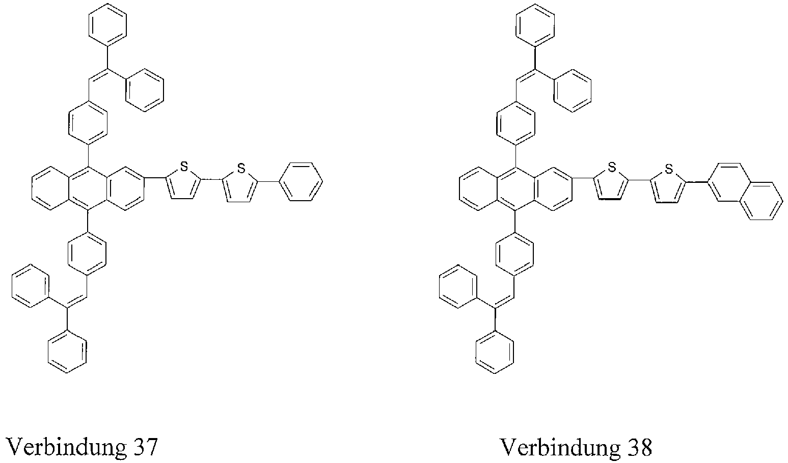
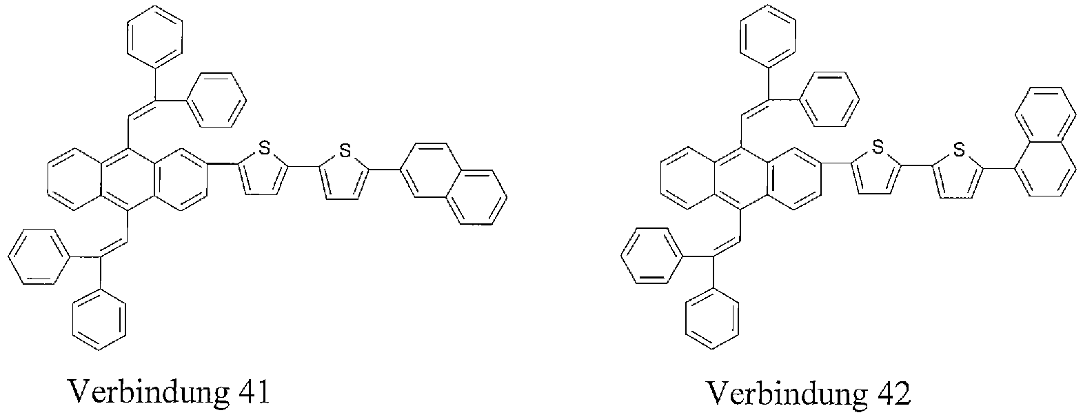
- One aspect of the present invention provides a compound selected from the group consisting of: Compound 1 Compound 2 Compound 3 Compound 4 Compound 5 Compound 6 Compound 7 Compound 8 Compound 9 Compound 10 Compound 11 Compound 12 Compound 13 Compound 14 Compound 15 Compound 16 Compound 17 Compound 18 Compound 19 Compound 20 Compound 21 Compound 22 Compound 23 Compound 24 Compound 25 Compound 26 Compound 27 Compound 28 Compound 29 Compound 30 Compound 31 Compound 32 Compound 33 Compound 34 Compound 35 Compound 36 Compound 37 compound 38 Compound 39 Compound 40 Compound 41 Compound 42 Compound 43 Compound 44 Compound 45 Compound 46 Compound 47 Compound 48 Compound 49 Compound 50 Compound 51 Compound 52 Compound 53 Compound 54 Compound 55 Compound 56 Compound 57 Compound 58 Compound 59 Compound 60 Compound 61 Compound 62 Compound 63 Compound 64 Compound 65 Compound 66 Compound 67 Compound 68 Compound 69 Compound 70 Compound 71 Compound 72 Compound 73 Compound 74 Compound
- the compound as previously defined is selected from the group consisting of Compounds 1 through 60.
- the compound as previously defined is selected from the group consisting of Compounds 1 through 24.
- the compound as previously defined Formula I is selected from the group consisting of Compounds 1, 4, 12, 14, 19, 21, 23, 25, 27 and 29.
- the compound has a melting point above about 300°C.
- the compound has a band-gap corresponding to visible light emission.
- the band-gap for the visible light emission is from about 1.8 eV to about 3.5 eV.
- Another aspect of the present invention provides a light-emitting material, which comprises one or more of the above-described compounds, each compound having a band gap.
- the light-emitting material further comprises one or more additional light-emitting compounds that are not the compound as previously defined, wherein each additional compound has a band gap.
- the band gap of at least one of the additional compound is from about 80 % up to 100 % of the value of the band gap of the compound previously described
- the light-emitting material further comprises one or more light-emitting compounds selected from the group consisting of BCzVBi, perylene, rubrene, DCJTB, quinacridone, coumarine, nile red, DCM1, DCM2, tetradiphenylamino pyrimido-pyrimidine, pyrydinothiadiazole and Compounds 201-220.
- a light-emitting material comprising one or more of the above-described compounds selected from the group consisting of Compounds 1 through 96; a hole-transporting material comprising one or more of the above-described compounds selected from the group consisting of Compounds 1 through 96; an electron-transporting material comprising one or more of the above-described compounds selected from the group consisting of Compounds 1 through 96.
- Another aspect of the present invention provides a solid film comprising one or more of the above-described compounds selected from the group consisting of Compounds 1 through 96.
- the one or more compounds in the solid film are in an amorphous form.
- the solid film further comprises one or more additional compounds that is not the compound selected from the group consisting of Compounds 1 through 96.
- At least one additional compound that is not the compound as previously defined has a band gap smaller than that of the compound previously defined.
- the band gap of the additional compound is from about 70 % up to 100% of the band gap of the compound selected from the group consisting of Compounds 1 through 96.
- the band gap of the additional compound is from about 90 % up to 100% of the band gap of the compound selected from the group consisting of Compounds 1 through 96.
- One compound selected from the group consisting of Compounds 1 through 96 is a host material in the solid film. At least one compound selected from the group consisting of Compounds 1 through 96 is a dopant in the solid material.
- One additional compound that is not the compound previously defined is a host material in the solid film. At least one additional compound that is not the compound previously defined is a dopant in the solid film. At least one additional compound is a light-emitting compound.
- Each additional compound that is not the compound previously defined has one or more properties selected from the group consisting of visible light emission, electron transportation, electron injection, hole transportation, and hole injection. At least one additional compound is a fluorescent or phosphorescent light-emitting compound.
- the solid film has a thickness from about 5 nm to about 100 nm.
- Each compound selected from the group consisting of Compounds 1 through 96 has one or more properties selected from the group consisting of visible light emission, electron transportation, electron injection, hole transportation, and hole injection. At least one compound as previsouly defined has a band gap corresponding to visible light emission.
- the solid film is formed by vapor deposition, inkjet printing or spin coating of the one or more compounds selected from the group consisting of Compounds 1 through 96 with or without a material that is not the compounds previously mentioned.
- the solid film comprising the light-emitting material.
- Another aspect of the present invention provides a method of making the above-described solid film.
- the method comprises: providing a support; and forming at least one layer comprising the one or more compounds therein over the support, wherein the at least one layer constitute the solid film.
- the layer is formed by physical vapor deposition, inkjet printing or spin coating of the compound over the support.
- an organic electroluminescent (“EL”) device which comprises: an anode; a cathode; and the above-described solid film located between the anode and cathode.
- the solid film serves one of more functions selected from the group consisting of light-emission, hole-injection hole-transportation, electron-transportation and electron-injection.
- the organic EL device further comprises one or more additional solid film between the anode and cathode.
- the organic EL device is supported by a substrate, and wherein the substrate contacts either the anode or the cathode.
- the solid film constitutes a light-emitting layer.
- the light-emitting layer comprises one or more fluorescent or phosphorescent light-emitting materials.
- the organic EL device further comprises one or more additional solid films between the anode and cathode.
- the organic EL device further comprises a hole-injecting layer, a hole-transporting or both between the anode and the light-emitting layer.
- the organic EL device further comprises an electron-injecting layer, an electron-transporting or both between the cathode and the light-emitting layer.
- the light-emitting layer comprises at least two compounds capable of emitting light therein. At least one compound selected from the group consisting of Compounds 1 through 96 has a band gap corresponding to visible light emission.
- the light-emitting layer further comprises at least one additional light-emitting compound.
- the additional light-emitting compound is different from a compound selected from the group consisting of Compounds 1 through 96.
- the additional light-emitting compound is also a compound selected from the group consisting of Compounds 1 through 96.
- the additional light-emitting compound has a quantum efficiency higher than that of the at least one compound selected from the group consisting of Compounds 1 through 96.
- the additional light-emitting compound has a band gap smaller than that of the at least one compound selected from the group consisting of Compounds 1 through 96
- the band gap of the additional compound is from about 70 % up to 100% of the band gap of the compound selected from the group consisting of Compounds 1 through 96.
- the band gap of the additional compound is from about 80 % up to 100% of the band gap of the compound selected from the group consisting of Compounds 1 through 96.
- the band gap of the additional compound is from about 90 % up to 100% of the band gap of the compound selected from the group consisting of Compounds 1 through 96.
- the additional light-emitting compound is a phosphorescent light-emitting compound.
- At least one compound is selected from the group consisting of Compounds 1 through 96.
- the compound previously described is selected from the group consisting of Compounds 1 through 60.
- the compound previously described is selected from the group consisting of Compounds 1 through 24.
- the compound previously described is selected from the group consisting of Compounds 1, 4, 12, 14, 19, 21, 23, 25, 27 and 29.
- the light-emitting layer further comprises therein one or more light-emitting compounds selected from the group consisting of BCzVBi, perylene, rubrene, DCJTB, quinacridone, coumarine, nile red, DCM1, DCM2, tetradiphenylamino pyrimido-pyrimidine, pyrydinothiadiazole and Compounds 201-220.
- Still another aspect of the present invention provides an electronic apparatus comprising a display, wherein the display comprises the above-described organic EL device with the above-described various features.
- Still another aspect of the present invention provides a method of generating visible light from the above-described organic EL device.
- the method comprises: applying electric power between the anode and cathode of the device; injecting electrons from the cathode toward the solid film; injecting holes from the anode toward the solid film; and allowing recombination of at least part of the injected electrons and holes in an area between the cathode and anode, thereby generating visible light from the area.
- One or more light-emitting materials are located in the area.
- the solid film constitutes a light-emitting layer. At least one compound selected from the group consisting of Compounds 1 through 96 is a light-emitting compound.
- the solid film further comprises an additional light-emitting compound therein.
- the additional light-emitting compound is not a compound selected from the group consisting of Compounds 1 through 96.
- the additional light-emitting compound has higher quantum efficiency than the compound selected from the group consisting of Compounds 1 through 96.
- the solid film serves one of more functions selected from the group consisting of light-emission, hole-injection hole-transportation, electron-transportation and electron-injection.
- Still another aspect of the present invention provides a method of manufacturing the above-described organic EL device.
- the method comprises: providing a substrate; forming a first conductive layer; forming the solid film; and forming a second conductive layer, wherein either of the first and second conductive layers corresponds to the anode or cathode.
- the formation of the solid film comprises vapor depositing, inkjet printing or spin-coating at least one compound selected from the group consisting of Compounds 1 through 96.
- the solid film so formed, at least one additional compound that is not a compound selected from the group consisting of Compounds 1 through 96 is incorporated.
- the method further comprises forming one or more additional solid films comprising organic compounds between the first and second conductive layers.
- One aspect of the present invention is directed to a novel group of compounds selected from the groups consisting of:
- the compounds as previously described can be synthesized in multi-step chemical reactions.
- the syntheses of the compounds are described by way of actual examples below.
- the certain intermediate compounds are first synthesized, and then the intermediate compounds are reacted together and/or modified.
- Some exemplary intermediate compounds are listed below as Compounds 101-123. In these compounds, "Br" may be substituted with any other reactive atoms or functional groups.
- Organic EL devices are made of, among other materials, one or more organic compounds.
- the organic compounds used in organic EL devices have various functions, including emission of light, facilitating injection of carriers from electrodes, facilitating transportation of injected carriers, hosting dopants, improving efficiency of light emission, and so forth.
- the organic compounds selected from the previously defined group according to one aspect of the present invention are compatible with applications in organic EL devices as they can perform one or more of the functions.
- many of the compounds selected from the group consisting of Compounds 1 through 96 are particularly useful as a light-emitting material. Further, many of such compounds are suitable as a host for hosting another light-emitting material called dopant.
- a host material for hosting a light-emitting dopant must have its own light-emitting property. The host material in an organic EL device has to energetically match with the dopant. Further, the host material has to be electrically stable in the organic EL devices.
- a number of compounds selected from the group consisting of Compounds 1 through 96 have the property of emitting visible light when appropriate energy is applied. These compounds have a band gap, which is difference between the lowest energy level of the conduction band and the highest energy level of the valance band, generally corresponding to the energy for visual light emission.
- the band gap of the compounds selected from the group consisting of Compounds 1 through 96 range from about 1.8 eV to about 3.0 eV.
- compounds selected from the group consisting of Compounds 1 through 96 can generate visible light of various colors ranging from generally bluish green to far red upon application of appropriate electric energy. The band gap corresponding to these color ranges are from about 2.8 eV to about 1.8 eV.
- These light-emitting compounds can host one or more matching dopants as will be further discussed below. Also, these compounds can emit its own colored light either as a sole light-emitting material or as a dopant to another host material.
- a host material and a dopant are to energetically match with each other.
- the band gap of the host material is required to be the same or greater than the band gap of the dopant so that the dopant can emit visible light. Further, it is preferred that the band gap of the host is only "slightly" greater than that of the dopant as will be further discussed.
- a number of the compounds selected from the group consisting of Compounds 1 through 96 advantageously generate colored lights, varying from bluish green to far red. Thus, there are many choices of different color-generating materials for either host or dopant among the compounds selected from the group consisting of Compounds 1 through 96. For example, when a dopant of a particular band gap is selected, then there would be choices of compounds selected from the group consisting of Compounds 1 through 96 that can energetically match with the dopant, vice versa.
- light-emitting molecules are electrically more stable than others.
- reactions of holes and electrons at or near the light-emitting molecules may electrochemically destroy or decompose the compounds, which can most likely cause increase of driving voltage of the device, drastic drop in the brightness of the emission or both.
- light-emitting materials either hosts or dopants, are selected from the electrically stable compounds.
- the new organic compounds according to one aspect of this invention show outstanding electrical stability as will be discussed below with reference to Examples.
- thermal stability of the compounds for use in organic EL devices is also important as quality of organic EL devices may deteriorate when they are subject to a high temperature.
- organic compounds exist in the form of amorphous thin films.
- the amorphous form of the compounds may crystallize when the temperature goes up above their glass transition temperature. Even partial crystallization of the compounds may cause an electrical short, resulting in the loss of electroluminescence. Crystallization in the amorphous films may also occur during the manufacturing process involving a high temperature.
- glass transition temperature of a compound must be higher than a temperature to which the thin film could possibly be subjected.
- organic EL compounds having a glass transition temperature of about 120°C or above are sufficient for use in organic EL devices.
- glass transition temperature of a compound has good correlation with melting point thereof, as well understood by ordinary skills in the relevant technology, the melting point is often used as a reference instead of glass transition temperature.
- the relationship between melting point and glass transition temperature is set forth in Molecular Design for Nonpolymeric Organic Dye Glasses with Thermal Stability, J. Phys. Chem. 97, 6240-6248 (1993 ), which is hereby incorporated herein by reference.
- many compounds selected from the group consisting of Compounds 1 through 96 have melting points sufficient to use in organic EL devices.
- the compounds selected from the group consisting of Compounds 1 through 96 have a melting point above about 300°C or a glass transition temperature above about 120°C, more preferably, the melting point is above about 350°C.
- Another aspect of the present invention is organic EL devices using the novel organic compounds described above.
- the new compounds have one or more properties of electroluminescence, hole injection, hole transportation, electron transportation and electron injection.
- Various organic EL devices can be constructed with one or more of the new organic compounds of the present invention in combination with any other compounds compatible with organic EL technology.
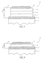
- FIG. 1-6 illustrate cross-sectional constructions of organic EL devices that can be built in accordance with the present invention.
- the same reference numbers are used to indicate like layers or components among the constructions.
- the term "layer” refers to a deposit, coat or film of one compound or a mixture of more than one compound. It should be noted that these constructions are not exhaustive variants of the organic EL devices in accordance of the present invention.
- the illustrated organic EL devices include a substrate 1, an anode 3, a cathode 15 and one or more layers located between the anode 3 and the cathode 15.
- the one or more intervening layers contain at least one of the compounds selected from the group consisting of Compounds 1 through 96.
- the one or more intervening layers include a hole-injecting layer 5, a hole-transporting layer 7, a light-emitting layer 9, an electron-transporting layer 11, an electron-injecting layer 13 and layers having functions of two or more of the foregoing layers.
- the substrate 1 ( Figures 1-6 ) supports the laminated structure of the organic EL device 10.
- the anode 3 ( Figures 1-6 ) and cathode 15 ( Figures 1-6 ) are electrically connected to an electric power source 17 ( Figures 1-6 ) via a switch 19 ( Figures 1-6 ), which is controlled by a controller (not shown).
- the electric power source is preferably a current source.
- the hole-injecting layer 5 ( Figures 1-3 ) is to facilitate the injection of holes from the anode 3 into the hole-transporting layer 7 ( Figures 1-5 ).
- the electron-injecting layer 13 ( Figures 1 and 4 ) is to facilitate the injection of electrons from the cathode 15 into the electron-transporting layer 13.
- the hole-transporting layer 7 is to accelerate movement of holes away from the anode 3 and/or the hole-injecting layer 5 toward the light-emitting layer 9 ( Figures 1-6 ).
- the electron-transporting layer 11 ( Figures 1, 2 , 4 and 5 ) is to accelerate movement of electrons away from the cathode 15 and/or the electron-injecting layer 13 toward the light-emitting layer 9 ( Figures 1-6 ).
- the light-emitting layer 9 is a layer particularly dedicated to the emission of visible light by the process of recombination of electrons and holes therein although it may have other functions as well.
- a light-emitting layer may not be included as a separate layer in an organic EL device, in which visible light is generated where light-emitting materials are doped.
- An organic EL device of the present invention preferably includes a separate light-emitting layer.
- a compound selected from the group consisting of Compounds 1 through 96 as previously defined advantageously forms the light-emitting layer.
- a compound different from the compound selected from the group consisting of Compounds 1 through 96 as previously defined form the light-emitting layer 9, while one or more compounds selected from the group consisting of Compounds 1 through 96 are used in one or more other layers of the organic EL device.
- the light-emitting layer 9 of organic EL devices may be composed of either a single light-emitting compound or a mixture of two or more materials.
- the most included compound is called a host while the other or the others are called dopants.
- both of the host and at least one dopant have the light-emitting property.
- Both of the host and at least one dopant may be selected from the compounds selected from the group consisting of Compounds 1 through 96.
- the host is selected from the compounds chosen from the group consisting of Compounds 1 through 96 while a dopant is selected from compounds not chosen from the previously defined group
- a compound not selected from the group consisting of Compounds 1 through 96 may be used as the host while a dopant is selected from the compounds selected from the group consisting of Compounds 1 through 96.
- the host material is selected from the compounds chosen from the group consisting of Compounds 1 through 96 with one or more dopant, whether the dopant is a compound belonging to the group previously defined.
- the compounds belonging to the previously defined group are selected preferably from Compounds 1-36, more preferably Compounds 4, 12, 14, 19, 21, 23, 25, 17 and 29.
- light-emitting compounds which are not selected from the group previously mentioned, for use in the light-emitting layer 9 include 8-hydroxyquinoline metal complexes including Alq3; carbazole compounds and derivatives thereof; dimerized styryl compounds ( U.S Patent No. 5,366,811 ); BAlq ( U.S. Patent No 5,150,006 ); 10-hydroxybenzo [h] quinoline-metal complexes ( U.S. Patent No.
- Organic EL devices of the present invention may be constructed with or without a dopant. Dopants are introduced to improve the light-emission efficiency, to tune the color of the emission, and/or to simply emit light from a layer having a non-fluorescent host. Dopants can be added to the light-emitting layer 9 and one or more of the other layers 5, 7, 11 and 13. More than one light-emitting material can be doped together in these layers for various purposes. Further, in an embodiment of the organic EL devices according to the present invention, the light-emitting layer 9 may be absent. In such constructions, one or more light-emitting dopants are necessarily put in one or more of the layers 5, 7, 11 or 13 to generate visible light therefrom.
- dopants for the light-emitting layer 9 are selected from light-emitting materials having higher quantum efficiency than the host material.
- the dopants have a quantum yield close to "1" in a dilute system. This means that most of the energy received from excitons contributes to the light emission rather than releasing it in other forms such as generating heat.
- dopants are selected such that they match energetically with the host material. Excitons are known to have a tendency to transfer their energy to a material having a smaller band gap among materials near the recombination location; thus, dopants are advantageously selected from the light-emitting materials having a band gap smaller than that of the host material.
- recombination may occur in the host molecules, and the energy of the generated excitons is transferred to the dopants.
- visible light is emitted from the dopant molecules.
- the energy of the excitons may be transferred to another dopant, where the light is emitted.
- dopants are preferably selected from a light-emitting materials having a band gap "slightly" smaller than that of the host material. Smaller band gap difference between host and dopant molecules provide more efficient energy transfer from the host molecule to the dopant molecules. In inefficient energy transfer, for example some hosts do not transfer the recombination energy to dopants and may generate its own light while dopants that received energy from other hosts also generates light. The resulting light is a mixture of the colors of host and dopant's, which is normally not desirable in creating full color display. Thus, when a dopant is determined, the host is selected from various compounds having a slightly larger band gap than that of the dopant, vice versa.
- the dopant's band gap can have any value from about 60 % up to 100 % of the value of the host's band gap, preferably, from about 80 % up to 100 %.
- the dopant is selected from the compounds chosen from the group consisting of Compounds 1 to 96 whether or not the host is a compound belonging to the previously defined group.
- the dopants are selected from Compounds 1-36 with or without dopants that are not selected from the group consisting of Compounds 1 to 96.
- the dopant is a compound not selected from the group consisting of Compounds 1 to 96 whether or not the host belongs to the previously defined group. Whether the dopant is a compound selected or not from the group consisting of Compounds 1 to 96 it preferably has fluorescent or phosphorescent property. Preferably, the dopant is a phosphorescent material, which converts triplet energy that would not be used in fluorescent materials into light via an internal process called "triplet to singlet transition". A general description of the triplet to singlet transition can be found in Nature (403,6771, 2000, 750-753 ), which is hereby incorporated herein by reference.
- the dopant is a light-emitting compound not selected from the group consisting of Compounds 1 to 96 whereas the host is a compound selected from the group consisting of Compounds 1 to 96.
- the host is chosen from the compounds selected from the group consisting of Compounds 1 to 96 having a matching band gap as discussed above.
- Persons of ordinary skill in the art would appreciate compounds not belonging to the previously defined group that can be used as dopants in the light-emitting layer 9 or other layers 3, 5, 7, 11 and 13.
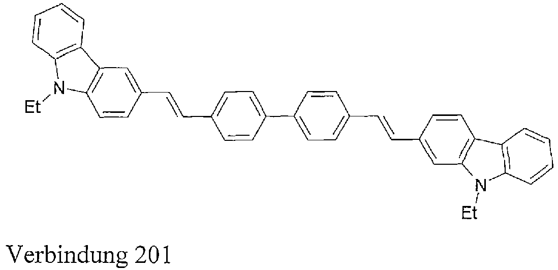
- Examples of doping materials not selected from the the group consisting of Compounds 1 to 96 are BCzVBi or 2,2'-([1,1'-biphenyl]-4,4'-diyldi-2,1-ethenediyl)bis[9-ethyl-9H-carbazole, perylene, rubrene, DCJTB or 2-(1,1-dimethylethyl)-6-[2-(2,3,6,7-tetrahydro-1,1,7,7-tetramethyl-1H,5H-benzo[ij]quinolizin-9-yl)ethenyl]-4H-pyran-4-ylidene]-propanedinitrile, quinacridone and its derivatives, coumarine and its derivatives, nile red, DCM1 or 2-[2-[4-(diethylamino)phenyl]ethenyl]-6-methyl-4H-pyran-4-ylidene]-propanedinitrile, DCM
- the substrate 1 is located on the side of the anode 3
- the substrate 1 may be located on the side of the cathode 15.
- the substrate 1 provides a support on which the laminated construction of the organic EL device can be build during the manufacturing.
- the substrate 1 functions as a protective layer for the construction of the organic EL device once manufactured.
- materials for the substrate 1 are selected from those, which can stand the conditions of manufacturing processes and usage of the organic EL devices. Persons of ordinary skill in the art would well appreciate what materials can satisfy the requirements based on the conditions.
- the substrate 1 is advantageously made of a transparent material to allow the visible light emitted from the light-emitting layer 9 to pass through.
- Transparent materials which can be used for the substrate 1, for example, include glass, quartz and any other appropriate natural or artificial materials. Preferably, glass is used for the substrate 1.
- the light can be emitted through the cathode 15 or any directions other than through the substrate 1.
- the substrate 1 is advantageously made of highly reflective material satisfying thermodynamic and mechanical requirements for forming the anode 3 thereon.
- semiconductor wafers, metal oxide, ceramic materials, and non-transparent plastics can be used as the substrate 1.
- a transparent substrate coated with a reflective material can also be used.
- the anode 3 is a conductive electrode electrically connected to the electric power source 17. Although not illustrated, the anode 3 may be constructed in multiple layers of materials. The thickness of the anode 3 may vary depending on the materials used and its layered structures. However, the anode 3 is advantageously from about 10 nm to about 1000 nm, preferably from about 10 nm to about 500 nm.
- the anode 3 requires a relatively large work function to favor injection of holes.
- the work function of materials for the anode 3 is about 4 eV or greater.
- conductive materials which can be used for the anode 3, include carbon; aluminum, vanadium, chromium, copper, zinc, silver, gold, similar metals, and alloys of the foregoing metals; zinc oxide, indium oxide, indium tin oxide (ITO), indium zinc oxide and similar tin oxide or tin oxide indium-based complex compounds; mixtures of oxides and metals, such as ZnO:Al, SnO 2 :Sb; and conductive polymers, such as poly(3-methylthiophene), poly[3,4-(ethylene-1,2-dioxy) thiophene], polypyrrole and polyaniline.
- Either transparent or non-transparent materials can be selected for the anode 3, depending upon the construction of the light passage in the organic EL device as discussed above in connection with the materials for the substrate 1.
- the anode 3 is made of ITO.
- ITO indium tin oxide
- the cathode 15 is also a conductive electrode electrically connected to the electric power source 17. Although not illustrated, the cathode 15 may be constructed in multiple layers of materials. The thickness of the cathode 15 may vary depending on the materials used and its layered structures. However, the cathode 15 is laminated generally from about 1 nm to about 10,000 nm, preferably from about 5 nm to about 5,000 nm.
- the cathode 15 requires a relatively small work function to favor injection of electrons.
- the work function of materials for the cathode 15 is about 4 eV or smaller.
- conductive materials, which can be used for the cathode 15, include magnesium, calcium, sodium, potassium, titanium, indium, yttrium, lithium, gadolinium, aluminum, silver, tin, lead, similar metals, and alloys of foregoing metals.
- Multi-layered cathode materials include LiF/Al and Li 2 O1Al.
- the cathode 15 is made of aluminum-lithium alloy, LiF/Al or Li 2 O/Al.
- Either transparent or non-transparent materials may be used for the cathode 15, depending upon the construction of the light passage in the organic EL device as discussed above. Those of ordinary skill in the art would appreciate any other materials that can be used in the cathode 15 and also the selection of appropriate cathode materials.
- the hole-injecting layer 5 has the function of enabling a large number of holes to be injected from the anode 3 at a low electric field applied to the device.
- the hole-injecting layer 5 advantageously is formed in the case where the interfacial strength between anode layer 3 and hole-transporting layer 7 is not strong enough.
- the hole-injecting layer 5 may be formed when the work function of the anode material is significantly different from the highest occupied molecular orbital (HOMO) level of the material of its neighboring layer 7, 9, 11 or 13.
- HOMO highest occupied molecular orbital
- the HOMO level of the hole-injecting material is advantageously located between the work function of the anode 3 and the HOMO level of the other neighboring layer 9, 11 or 13, although not limited thereto.
- the HOMO level of the compounds for hole-injecting layer 5 ranges from about -4.0 eV to about -6.0 eV.
- the hole-injecting material is preferred to be transparent when the construction of the organic EL device allows the light emission through the substrate 1. In otherwise constructions, the hole-injecting material is advantageously non-transparent.
- the hole-injecting layer 5 may be made of one or more of the organic compounds selected from the group consisting of Compounds 1 to 96. In this embodiment, one or more compounds that are not selected from the group consisting of Compounds 1 to 96 may be added. In another embodiment of organic EL devices, one or more compounds selected from the group consisting of Compounds 1 to 96 are used in one or more other layers of the device, while one or more compounds not selected from the previously defined group form the hole-injecting layer 5. Those of ordinary skill in the art will appreciate compounds not belonging to the group previously mentioned that can be used in the hole-injecting layer 5 and also the selection of appropriate materials.
- the compounds not selected from the group consisting of Compounds 1 to 96 that can be used in hole-injecting layer 5 include, for example, metal porphyrine ( U.S. Patent Nos. 4,720,432 and 4,356,429 ); oligothiophene ( U.S. Patent No. 5,540,999 ); arylamines and derivatives thereof ( U.S. Patent Nos.
- the hole-transporting layer 7 has the function to smoothly transfer the holes from the hole-injecting layer 5 or from anode 3 (in the absence of the hole-injecting layer 5) toward the light-emitting layer 9 or toward an area where light-emitting materials are doped.
- materials good for use in the hole-transporting layer 7 are those having high hole mobility therein.
- the high mobility of holes in those compounds will reduce the driving voltage of an organic EL device because holes in the compounds having high hole mobility are prone to move at a low electric potential difference.
- the compounds for use in the hole-transporting layer 7 have hole mobility of about 1x10 -7 cm 2 /Vs or greater.
- the hole-transporting layer 7 has the function to inhibit electrons from moving into it from its neighboring layer 9, 11, or 13 on the side of the cathode 15. Materials having low mobility of electrons is preferred.
- the hole-transporting layer 7 functions for both the hole injection and hole transportation. In this case, materials having hole-injecting property discussed above would also be preferred.
- the hole-transporting layer 7 can be made of one or more of the organic compounds selected from the group consisting of Compounds 1 to 96. In this embodiment, one or more compounds not selected from the group consisting of Compounds 1 to 96 may be added. In another embodiment of organic EL devices, one or more compounds selected from the group consisting of Compounds 1 to 96 are used in one or more other layers of the device, while one or more compounds not selected from the group previously defined form the hole-transporting layer 7.
- the compounds not selected from the group consisting of Compounds 1 to 96 that can be used in the hole-transporting layer 7 include, for example, arylamine derivatives, conjugated poylmers, block co-polymers with conjugated and non-conjugated repeating units, and the like.
- derivatives of the arylamine, 4,4'-bis[N-(1-naphthyl)-N-phenylamino]biphenyl (NPB) is used for the hole-transporting layer 7.
- NPB 4,4'-bis[N-(1-naphthyl)-N-phenylamino]biphenyl
- the electron-transporting layer 11 contains a material prone to transfer electrons injected from the electron injecting layer 13 or the cathode 15 (in the absence of the electron-injecting layer 13) to the light-emitting layer 9 or to an area where a light-emitting material is doped. If the material meets the requirements for the electron-injecting layer 13, the functions of electron-transportation and injection can be combined in a singl layer as shown Figure 2 .
- compounds having high electron mobility is used as an electron-transporting material because high mobility of electrons will reduce the driving voltage of the organic EL devices using the compounds. Injected electrons in such compounds having high electron mobility are prone to move at a low electric potential difference.
- the compounds having electron mobility of about 1x10 -7 cm 2 /Vs or greater can be used for electron transportation.
- the electron-transporting layer 11 also has the function of blocking holes to move thereinto. Materials having low mobility of holes are preferred. Compounds having hole mobility of about 1 x 10 -3 cm 2 /VS or less are preferred.
- the electron-transporting layer 11 can be made of one or more of the compounds selected from the group consisting of Compounds 1 to 96. One or more compounds that are not selected from the group consisting of Compounds 1 to 96 may be added. In another embodiment of organic EL devices, one or more compounds selected from the group consisting of Compounds 1 to 96 are used in one or more other layers of the EL device, while one or more compounds not belonging to the group previously defined form the electron-transporting layer 11. Those of ordinary skill in the art will appreciate compounds not belonging to the group previously defined that can be used in the electron-transporting layer 11 and also the selection of appropriate materials.
- the compounds not belonging to the group previously defined that can be used in the electron-transporting layer 11 include, for example, aluminum complexes of 8-hydroxyquinoline; organometallic complex compounds including Alq3 ( U.S. Patent No. 5,061,569 and U.S. Patent Application No. 09/540837 ); organic radical compounds ( U.S. Patent No. 5,811,833 ); hydroxyflavon-metal complexes ( U.S. Patent Nos. 5,817,431 and 5,516,577 , Japanese Unexamined Patent Publications 2001-076879 , 2001-123157 and 1998-017860 , and Organic Light-emitting Diodes using 3-or 5-hydroxyflavone-metal Complexes, Appl. Phys. Lett. 71 (23), 3338 (1997 ).
- the referenced documents are hereby incorporated herein by reference.
- the electron-injecting layer 13 is generally to faciliate injection of a large number of electrons from the cathode 15 at a low electric field applied across the device.
- the electron-injecting layer 13 may be provided when the work function of the cathode 15 significantly differs from the lowest unoccupied molecular orbital (LUMO) level of the other neighboring layer 5, 7, 9 or 11. Much difference in the energy level act as an electric potential barrier of the electron injection.
- An electron-injecting layer reduces the electric potential barrier and facilitates the electron injection in the device.
- the electron-injecting layer 13 may also be introduced to prevent excitons generated in the neighboring layer 5, 7, 9 or 11 from moving toward the cathode layer 15.
- the electron-injecting layer 13 may be provided to avoid damaging the neighboring layer 5, 7, 9 or 11 in the course of the deposition of the cathode layer 15.
- the LUMO level of the electron-injecting material is advantageously located between the work function of the cathode material and the LUMO level of the other neighboring layer 5, 7, 9 or 11, preferably near the middle of the two.
- the LUMO level of compounds used for electron injection ranges from about -2.5 eV to about -4.0 eV.
- the electron-injecting layer 13 is required to have strong interface with the cathode layer 15.
- the electron-injecting layer 13 can be made of one or more of the compounds selected from the group consisting of Compounds 1 to 96. One or more of the compounds not selected from the previously defined group may be added. In another embodiment of organic EL devices, one or more compounds according to the present invention are used in one or more other layers of the organic EL device, while one or more compounds not selected from the group consisting of Compounds 1 to 96 form the electron-injecting layer 13. Those of ordinary skill in the art will appreciate compounds not belonging to the previously defined group that can be used in the electron-injecting layer 13 and also the selection of appropriate materials.
- the compounds not selected from the group consisting of Compounds 1 to 96 that can be used in the electron-injecting layer 13 include, for example, aluminum complexes of 8-hydroxyquinoline, organometallic complex compounds including Alq3, organic radical compounds ( U.S. Patent No. 5,811,833 ); 3-or 5-hydroxyflavone-metal complexes ( Organic Light-emitting Diodes using 3- or 5-hydroxyflavone-metal Complexes, Appl. Phys. Lett.
- Various layers of the organic EL devices of the present invention can be produced by utilizing any known film forming techniques, including physical vapor deposition (PVD), chemical vapor deposition (CVD), spin coating, inkjet printing, screen-printing, roll-coating. These techniques are generally described in the following publications, which are hereby incorporated herein by reference: Applied Physics Letters, 73, 18, 1998, 2561-2563 Applied Physics Letters, 78, 24, 2001, 3905-3907 .].
- layers containing one or more compounds selected from the group consisting of Compounds 1 to 96 may be formed on a support using PVD, CVD, spin coating, inkjet printing.
- a layer containing one or more compounds selected from the group consisting of Compounds 1 to 96 is produced using PVD, spin coating or inkjet printing, more preferably, PVD.
- Spin coating or inkjet printing can be preferably utilized for the formation of a layer containing one or more compounds which are selected from the group consisting of Compounds 1 to 96 and have one or more C10-C20 linear chains therein.
- 2,6-Diaminoanthraquinone (23.8 g, 100 mmol) was dispersed in 48 wt% of a hydrogen bromide aqueous solution.
- Sodium nitrite NaNO 2 , 14.1 g, 204 mmol
- a solution of copper bromide (CuBr, 29.5 g, 206 mmol) dissolved in 48 wt% of a hydrogen bromide aqueous solution (63 mL) was slowly added to the mixture together with a small amount of ethanol (50 mL). The temperature of the resulting mixture was slowly elevated and then the mixture was slowly refluxed.
- 2-Bromo biphenyl (8.83 mL, 51.2 mmol) was dissolved in dry tetrahydrofurane (THF, 200 mL) under a nitrogen atmosphere at room temperature. The solution is cooled to -78°C in a cooling bath. T-butyl lithium (60 mL, 1.7 M pentane solution) was slowly added to the solution at -78°C, and the resulting mixture was stirred for about 40 minutes at the same temperature. Thereafter, Compound 101 (7.50 g, 20.5 mmol) was added to the mixture at the same temperature. The cooling bath was removed, and the mixture was stirred at room temperature for about 15 hours.
- THF dry tetrahydrofurane
- Compound 105 (6.00 g, 10.1 mmol) was dispersed in 300 mL of acetic acid under a nitrogen atmosphere. Potassium iodide (16.8 g, 101 mmol) and sodium hypophosphite hydrate (17.7g, 167 mmol) were added thereto. The resulting mixture was agitated while boiling for 3 hours. After cooling to room temperature, the mixture was filtered and washed with water and methanol, and then vacuum dried to obtain Compound 106 (5.0 g, 88%) in a light yellow color.
- Compound 105 (9.5 g, 16 mmol) was dispersed in 100 mL of acetic acid. 5 drops of concentrated sulfuric acid were added to the dispersion. The mixture was refluxed for 3 hours, and then was cooled to room temperature. Precipitate was filtered, washed with acetic acid, and then washed with water and ethanol in this order. After drying, the solid was purified by sublimation to obtain Compound 107 (8.0 g, 89%) in a white solid form.
- the organic extract was dried over magnesium sulfate and concentrated under reduced pressure.
- the crude product was dissolved in diethyl ether, and then petroleum ether was added thereto.
- the mixture was agitated for several hours to obtain a solid compound.
- the solid was filtered and vacuum dried to obtain dinaphthyl dialcohol (11.2 g, 93%).
- the dinaphtyl dialcohol (11.2 g, 20.5 mmol)) was dispersed in 600 mL of acetic acid under a nitrogen atmosphere, to which potassium iodide (34.2 g, 206 mmol) and sodium hypophosphite hydrate (36.0 g, 340 mmol) were added.
- the resulting mixture was agitated while boiling for about 3 hours. After cooling to room temperature, the mixture was filtered and washed with water and methanol, and then vacuum dried to obtain Compound 109 (10.1 g, 96%) a light yellow color.
- the 2-(2-anthraquinone)-5-(4-formylphenyl)thiophene (1.70 g, 4.31 mmol) was mixed with N-phenyl-1,2-phenylenediamine (0.87 g, 4.74 mmol) in a mixture of 50 mL of toluene and 5 mL of acetic acid. The resulting mixture was refluxed for about 16 hours and cooled to room temperature. The formed solid was filtered, washed with acetic acid, and dried to obtain a solid of Compound 123 (0.75 g, 32%).
- the dialcohol compound (0.80 g, 0.98 mmol) was dispersed in acetic acid (100 mL) under a nitrogen atmosphere. Potassium iodide (1.66 g, 10 mmol) and sodium hypophosphite hydrate (1.76 g, 20 mmol) were added to the dispersion. The mixture was boiled for about 3 hours with continuous stirring and then cooled to room temperature. The mixture was filtered and washed with water, and then vacuum dried to obtain Compound 29 (0.80 g).
- Example 33 Organic EL Device with Light-Emitting Layer Using Compound 12
- a glass substrate coated with about 1500 ⁇ of ITO (indium tin oxide) was cleaned in an ultrasonic bath filled with a detergent solution. After the ultrasonic cleaning for about 30 minutes, the substrate was washed with distilled water twice for about 10 minutes each time to remove remaining detergent from the substrate. The substrate was further cleaned with in the order of isopropyl alcohol, acetone and methanol in an ultrasonic bath. After drying the in the air, the substrate was transferred into a plasma cleaning chamber connected with a thermal vacuum evaporator. The substrate was further cleaned in an oxygen plasma condition for about 5 minutes and the cleaning chamber was evacuated by a turbo-molecular pump to transfer the substrate to the thermal vacuum evaporator.
- ITO indium tin oxide
- hexanitrile hexaazatriphenylene was deposited as a hole-injecting material by thermal vacuum evaporation at about 5x 10 -7 torr.
- about 600 ⁇ of NPB, a hole-transporting material was deposited on the hole-injecting layer, which was followed by the deposition of about 200 A thickness of Compound 12 as the light-emitting material.
- Compound 301 (2-[4-[(N-phenylbenzimidazol-2-yl)phenyl-9,10-bis(2-naphtyl)anthracene) was formed as an electron-transporting and/or electron-injecting layer. Then, about 5 ⁇ thickness of lithium fluoride and about 2500 ⁇ of aluminum were deposited on the electron-transporting/injecting layer to form a LiF/Al bilayer cathode. The deposition rates of the organic materials were maintained at about 1A/sec, for the lithium fluoride at about 0.2 A/sec and for the aluminum at about 3 ⁇ 7 A/sec.
- An organic light-emitting diode was fabricated in the same manner in as described in Example 33 except that Compound 21 and Alq3 were used as the light-emitting material and electron transporting/injecting material respectively instead of Compound 12 and Compound 301.
- Compound 21 and Alq3 were used as the light-emitting material and electron transporting/injecting material respectively instead of Compound 12 and Compound 301.
- Example 35 Organic EL Device with Light-Emitting Layer Using Compound 19
- An organic light-emitting diode was fabricated in the same manner in as described in Example 34 except that Compound 19 was used as the light-emitting material instead of Compound 21.
- Compound 19 was used as the light-emitting material instead of Compound 21.
- 50 mA/cm 2 of constant DC current density it took 19.8 hours until the brightness drops to 90% level of the initial brightness.
- Example 36 Organic EL Device with Ligt-Emitting Layer Using Compound 14
- An organic light-emitting diode was fabricated in the same manner in as described in Example 34 except that Compound 14 was used as the light-emitting material instead of Compound 21.
- Compound 14 was used as the light-emitting material instead of Compound 21.
- At 50 mA/cm 2 of constant DC current density it took 10.6 hours until the brightness drops to 90% level of the initial brightness.
- Example 37 Organic EL Device with Light-Emitting Layer Using Compound 12 and DCJTB
- An organic light-emitting diode was fabricated in the same manner in as described in Example 33 except that DCJTB (2 wt.%) was co-deposited with Compound 12 in which Compound 12 serves as a host and DCJTB service a dopant.
- DCJTB 2 wt.%
- Compound 12 serves as a host and DCJTB service a dopant.
- At 50 mA/cm 2 of constant DC current density it took 132.5 hours until the brightness drops to 90% level of the initial brightness.
- Example 38 Organic EL Device with Light-Emitting Layer Using Alq3
- An organic light-emitting diode was fabricated in the same manner in as described in Example 33 except that 500 ⁇ of Alq3 was deposited in replace of both the light-emitting layer of Compound 12 and the electron-transporting/injecting layer of Compound 301.
- 50 mA/cm 2 of constant DC current density it took 1 hour until the brightness drops to 90% level of the initial brightness.
- electrical stability of materials used in light-emission is one of the very important characteristics in that it can determine the lifetime and driving voltage of organic EL devices. For example, if light-emitting material of an organic EL device is not electrically stable, the material may decompose during the course of electroluminescence processes, resulting in drop of brightness and requiring higher driving voltage. It has been known that Alq3 is very stable among organic EL compounds used in organic EL devices.
- Electrical stability of organic EL compounds are normally determined or compared in terms of the time period for which brightness of light emission from a light-emitting layer made of a material drops to a certain level, for example 90% of the initial brightness, when a constant current density is applied to the device.
- the time for 10% of initial brightness drop was measured for organic EL devices having various light-emitting materials.
- Examples 33-37 used compounds satisfying Formula I in light-emitting layers whereas Example 38 used Alq3.
- the time for the 10% drop of the initial brightness in Examples 33-37 are extraordinarily higher than that of Alq3 of Example 38.
- the use of organic compounds selected from the group consisting of Compounds 1 to 96 in organic EL devices, particularly as the light-emitting material would substantially improve organic EL devices in respect of driving voltage and device lifetime.
Landscapes
- Chemical & Material Sciences (AREA)
- Organic Chemistry (AREA)
- Physics & Mathematics (AREA)
- Spectroscopy & Molecular Physics (AREA)
- Engineering & Computer Science (AREA)
- Materials Engineering (AREA)
- Optics & Photonics (AREA)
- Electroluminescent Light Sources (AREA)
- Plural Heterocyclic Compounds (AREA)
- Heterocyclic Compounds Containing Sulfur Atoms (AREA)
Claims (21)
- Verbindung, die ausgewählt ist aus der Gruppe bestehend aus:





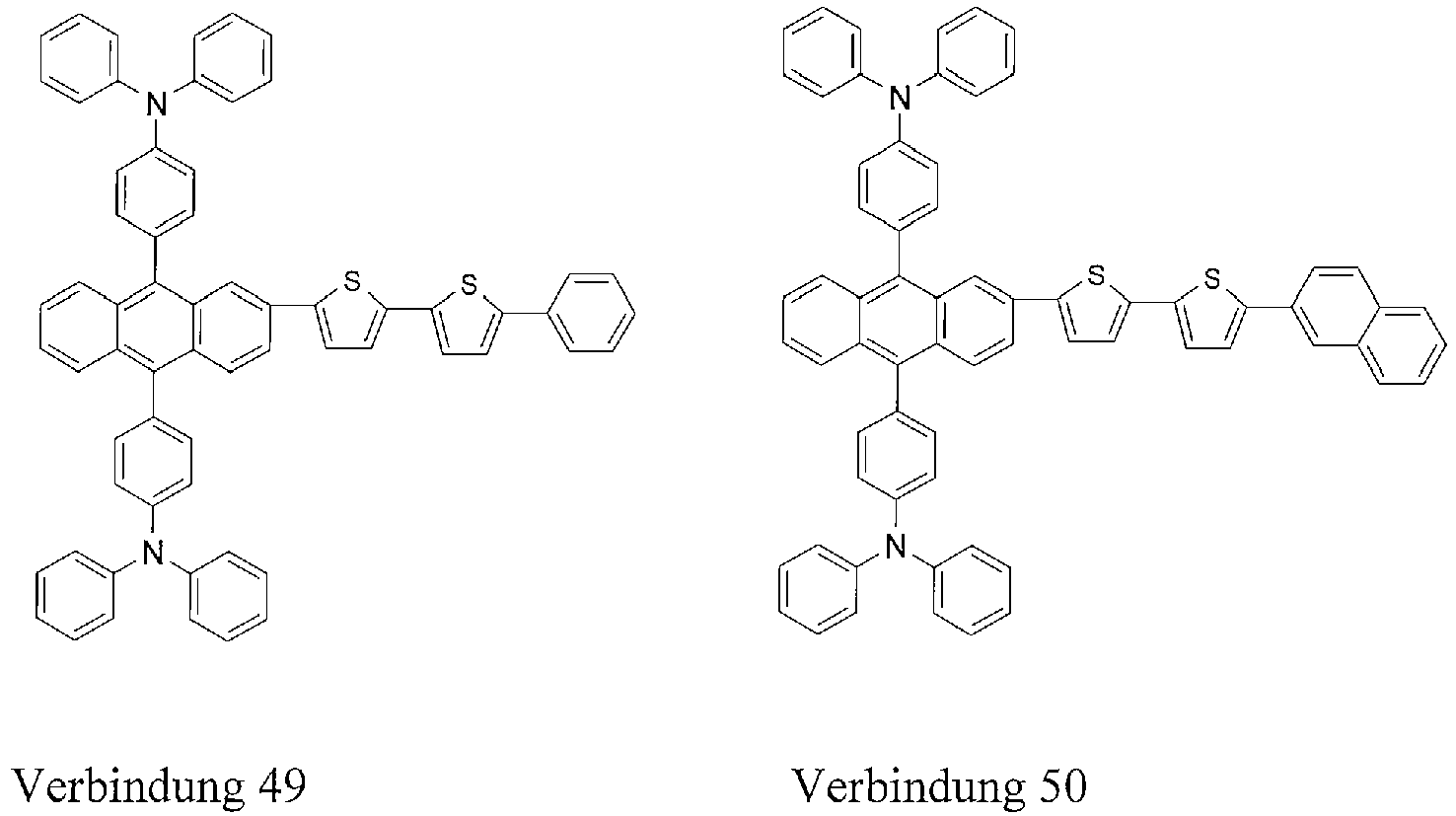
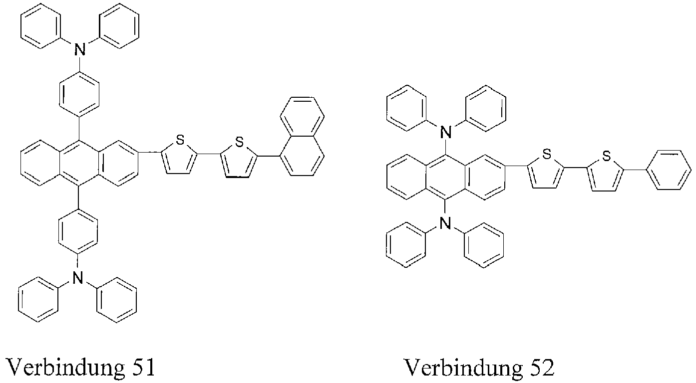


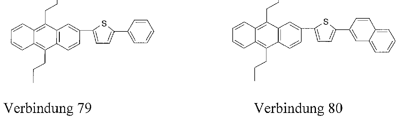


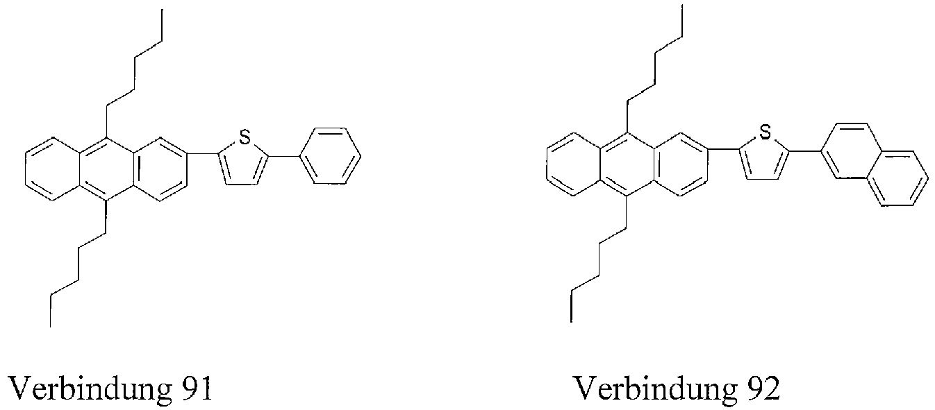


- Lichtemittierendes Material, das eine oder mehrere der Verbindungen von Anspruch 1 umfasst.
- Lichtemittierendes Material nach Anspruch 2, ferner umfassend eine oder mehrere zusätzliche lichtemittierende Verbindungen, die nicht die Verbindung von Anspruch 1 sind, wobei jede zusätzliche Verbindung einen Bandabstand hat.
- Lichtemittierendes Material nach Anspruch 3, wobei der Bandabstand mindestens einer der zusätzlichen Verbindungen von etwa 80 % bis 100 % des Wertes des Bandabstands der Verbindung von Anspruch 1 beträgt.
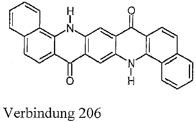
- Lichtemittierendes Material nach Anspruch 3 oder 4, ferner umfassend eine oder mehrere lichtemittierende Verbindungen, die aus der aus BCzVBi, Perylen, Rubren, DCJTB, Chinacridon, Cumarin, Nilrot, DCM1, DCM2, Tetradiphenylamino pyridopyrimidin, Pyridinthiadiazol und den Verbindungen 201-220 bestehenden Gruppe ausgewählt sind:


- Organische elektrolumineszierende ("EL") Vorrichtung, umfassend:eine Anode;eine Kathode; undmindestens eine zwischen der Anode und der Kathode befindliche Schicht,wobei die mindestens eine Schicht mindestens eine Verbindung gemäß Anspruch 1 umfasst.
- Organische EL-Vorrichtung nach Anspruch 6, wobei die mindestens eine Schicht eine Schicht umfasst, die einer oder mehreren Funktionen dient, die aus der aus Lichtemission, Löcherinjektion, Löchertransport, Elektronentransport und Elektroneninjektion bestehenden Gruppe ausgewählt sind.
- Organische EL-Vorrichtung nach Anspruch 6 oder 7, wobei die organische EL-Vorrichtung von einem Substrat getragen wird, und wobei das Substrat entweder die Anoder oder die Kathode berührt.
- Organische EL-Vorrichtung nach einem der Ansprüche 6 bis 8, wobei die mindestens eine Schicht eine lichtemittierende Schicht umfasst.
- Organische EL-Vorrichtung nach Anspruch 9, wobei die lichtemittierende Schicht ein oder mehrere fluoreszierende oder phosphoreszierende lichtemittierende Materialien umfasst.
- Organische EL-Vorrichtung nach Anspruch 9 oder 10, ferner umfassend eine löcherinjizierende Schicht, eine löchertransportierende Schicht oder beides zwischen der Anode und der lichtemittierenden Schicht.
- Organische EL-Vorrichtung nach einem der Ansprüche 9 bis 11, ferner umfassend eine elektroneninjizierende Schicht, eine elektronentransportierende Schicht oder beides zwischen der Kathode und der lichtemittierenden Schicht.
- Organische EL-Vorrichtung nach Anspruch 9 bis 12, wobei die lichtemittierende Schicht mindestens zwei Verbindungen umfasst, die darin Licht emittieren können.
- Organische EL-Vorrichtung nach einem der Ansprüche 6 bis 13, wobei mindestens eine Verbindung von Anspruch 1 einen der Emission von sichtbarem Licht entsprechenden Bandabstand besitzt.
- Organische EL-Vorrichtung nach einem der Ansprüche 6 bis 14, wobei die lichtemittierende Schicht ferner mindestens eine zusätzliche lichtemittierende Verbindung umfasst, welche die Verbindung von Anspruch 1 oder nicht die Verbindung von Anspruch 1 ist.
- Organische EL-Vorrichtung nach Anspruch 15, wobei die zusätzliche lichtemittierende Verbindung eine Quanteneffizienz besitzt, die höher ist als die der mindestens einen Verbindung von Anspruch 1.
- Organische EL-Vorrichtung nach Anspruch 15 oder 16, wobei die zusätzliche lichtemittierende Verbindung einen Bandabstand besitzt, der kleiner ist als der Bandabstand der mindestens einen Verbindung von Anspruch 1.
- Organische EL-Vorrichtung nach Anspruch 17, wobei der Bandabstand der zusätzlichen Verbindung von etwa 70 % bis 100 % des Bandabstands der Verbindung von Anspruch 1 beträgt.
- Organische EL-Vorrichtung nach einem der Ansprüche 15 bis 18, wobei die zusätzliche lichtemittierende Verbindung eine phosphoreszierende lichtemittierende Verbindung ist.
- Organische EL-Vorrichtung nach einem der Ansprüche 6 bis 19, wobei die lichtemittierende Schicht darin ferner eine oder mehrere lichtemittierende Verbindungen umfasst, die aus der aus BCzVBi, Perylen, Rubren, DCJTB, Chinacridon, Cumarin, Nilrot, DCM1, DCM2, Tetradiphenylamino pyridopyrimidin, Pyridinthiadiazol und den Verbindungen 201-220 bestehenden Gruppe ausgewählt ist:




- Elektronisches Gerät umfassend ein Display, wobei das Display die organische EL-Vorrichtung nach einem der Ansprüche 6 bis 19 und 20 umfasst.
Applications Claiming Priority (5)
| Application Number | Priority Date | Filing Date | Title |
|---|---|---|---|
| KR20020025084 | 2002-05-07 | ||
| KR2002025084 | 2002-05-07 | ||
| KR1020030010439A KR20030087522A (ko) | 2002-05-07 | 2003-02-19 | 새로운 유기발광층용 물질 및 이를 이용한 유기 발광 소자 |
| KR2003010439 | 2003-02-19 | ||
| PCT/KR2003/000899 WO2003095445A1 (en) | 2002-05-07 | 2003-05-06 | New organic compounds for electroluminescence and organic electroluminescent devices using the same |
Publications (2)
| Publication Number | Publication Date |
|---|---|
| EP1501821A1 EP1501821A1 (de) | 2005-02-02 |
| EP1501821B1 true EP1501821B1 (de) | 2016-07-20 |
Family
ID=29422501
Family Applications (1)
| Application Number | Title | Priority Date | Filing Date |
|---|---|---|---|
| EP03723417.6A Expired - Lifetime EP1501821B1 (de) | 2002-05-07 | 2003-05-06 | Neue organische verbindungen für die elektrolumineszenz und organisch-elektrolumineszente vorrichtungen, in denen diese verbindungen verwendet werden |
Country Status (8)
| Country | Link |
|---|---|
| US (2) | US7485733B2 (de) |
| EP (1) | EP1501821B1 (de) |
| JP (1) | JP2005531552A (de) |
| KR (1) | KR100578424B1 (de) |
| CN (1) | CN1556803A (de) |
| AU (1) | AU2003230308A1 (de) |
| TW (1) | TWI288774B (de) |
| WO (1) | WO2003095445A1 (de) |
Families Citing this family (133)
| Publication number | Priority date | Publication date | Assignee | Title |
|---|---|---|---|---|
| US7560175B2 (en) * | 1999-12-31 | 2009-07-14 | Lg Chem, Ltd. | Electroluminescent devices with low work function anode |
| KR100721656B1 (ko) * | 2005-11-01 | 2007-05-23 | 주식회사 엘지화학 | 유기 전기 소자 |
| US6998487B2 (en) * | 2001-04-27 | 2006-02-14 | Lg Chem, Ltd. | Double-spiro organic compounds and organic electroluminescent devices using the same |
| US6998068B2 (en) * | 2003-08-15 | 2006-02-14 | 3M Innovative Properties Company | Acene-thiophene semiconductors |
| JP4045932B2 (ja) * | 2002-11-21 | 2008-02-13 | コニカミノルタホールディングス株式会社 | 有機エレクトロルミネッセンス素子及び表示装置 |
| CN100508238C (zh) * | 2004-05-11 | 2009-07-01 | Lg化学株式会社 | 有机电子器件 |
| US7625501B2 (en) | 2004-05-18 | 2009-12-01 | Ifire Ip Corporation | Color-converting photoluminescent film |
| JP2006028054A (ja) * | 2004-07-14 | 2006-02-02 | Konica Minolta Holdings Inc | 有機薄膜トランジスタ材料、有機薄膜トランジスタ、電界効果トランジスタ及びスイッチング素子 |
| EP1794255B1 (de) * | 2004-08-19 | 2016-11-16 | LG Chem, Ltd. | Organische lichtemittierende vorrichtung mit pufferschicht und herstellungsverfahren dafür |
| JP4972288B2 (ja) * | 2004-08-30 | 2012-07-11 | 富士フイルム株式会社 | 撮像素子 |
| US7355199B2 (en) * | 2004-11-02 | 2008-04-08 | E.I. Du Pont De Nemours And Company | Substituted anthracenes and electronic devices containing the substituted anthracenes |
| US8927114B2 (en) * | 2004-11-30 | 2015-01-06 | Semiconductor Energy Laboratory Co., Ltd. | Light emitting element and electronic device using the same |
| JP4790260B2 (ja) * | 2004-12-22 | 2011-10-12 | 出光興産株式会社 | アントラセン誘導体を用いた有機エレクトロルミネッセンス素子 |
| US20060182994A1 (en) * | 2005-01-18 | 2006-08-17 | Yukinari Sakamoto | Anthracene derivative, organic electroluminescent device, and display unit |
| SE528408C2 (sv) * | 2005-03-07 | 2006-11-07 | Interactive Inst Ii Ab | En metod och en anordning för visuell indikering av ström- eller effektförbrukning i en elkabel |
| EP1888706B1 (de) * | 2005-05-03 | 2017-03-01 | Merck Patent GmbH | Organische elektrolumineszenzvorrichtung und in deren herstellung verwendete boronsäure- und borinsäure-derivate |
| US20060286405A1 (en) | 2005-06-17 | 2006-12-21 | Eastman Kodak Company | Organic element for low voltage electroluminescent devices |
| KR101139038B1 (ko) * | 2005-06-28 | 2012-05-02 | 삼성전자주식회사 | 피리미도피리미딘 유도체 및 이를 이용한 유기 박막 트랜지스터 |
| TWI321968B (en) | 2005-07-15 | 2010-03-11 | Lg Chemical Ltd | Organic light meitting device and method for manufacturing the same |
| DE102005040411A1 (de) | 2005-08-26 | 2007-03-01 | Merck Patent Gmbh | Neue Materialien für organische Elektrolumineszenzvorrichtungen |
| US20070116984A1 (en) * | 2005-09-21 | 2007-05-24 | Doosan Corporation | Spiro-compound for electroluminescent display device and electroluminescent display device comprising the same |
| US20070092753A1 (en) * | 2005-10-26 | 2007-04-26 | Eastman Kodak Company | Organic element for low voltage electroluminescent devices |
| KR100890862B1 (ko) * | 2005-11-07 | 2009-03-27 | 주식회사 엘지화학 | 유기 발광 소자 및 이의 제조 방법 |
| EP1948755B1 (de) * | 2005-11-18 | 2012-07-18 | LG Chem, Ltd. | Emittierendes material und organische lichtemittierende diode damit |
| US8795847B2 (en) | 2005-12-08 | 2014-08-05 | Merck Patent Gmbh | Materials for organic electroluminescent devices |
| US20070141393A1 (en) * | 2005-12-21 | 2007-06-21 | Eastman Kodak Company | Amino anthracene compounds in OLED devices |
| EP1971664B1 (de) * | 2006-01-13 | 2015-09-09 | LG Chem, Ltd. | Emittierende materialien und organische lichtemittierende vorrichtung damit |
| US8680693B2 (en) * | 2006-01-18 | 2014-03-25 | Lg Chem. Ltd. | OLED having stacked organic light-emitting units |
| JP5683104B2 (ja) | 2006-03-21 | 2015-03-11 | ノヴァレッド・アクチエンゲゼルシャフト | ドープされた有機半導体材料の製造方法及びそのために用いられる配合物 |
| DE102006013802A1 (de) * | 2006-03-24 | 2007-09-27 | Merck Patent Gmbh | Neue Materialien für organische Elektrolumineszenzvorrichtungen |
| US7608679B2 (en) * | 2006-03-31 | 2009-10-27 | 3M Innovative Properties Company | Acene-thiophene copolymers |
| US7667230B2 (en) * | 2006-03-31 | 2010-02-23 | 3M Innovative Properties Company | Electronic devices containing acene-thiophene copolymers |
| US7495251B2 (en) * | 2006-04-21 | 2009-02-24 | 3M Innovative Properties Company | Electronic devices containing acene-thiophene copolymers with silylethynyl groups |
| US7666968B2 (en) * | 2006-04-21 | 2010-02-23 | 3M Innovative Properties Company | Acene-thiophene copolymers with silethynly groups |
| US20070252517A1 (en) * | 2006-04-27 | 2007-11-01 | Eastman Kodak Company | Electroluminescent device including an anthracene derivative |
| DE102006025846A1 (de) | 2006-06-02 | 2007-12-06 | Merck Patent Gmbh | Neue Materialien für organische Elektrolumineszenzvorrichtungen |
| KR101304697B1 (ko) * | 2006-06-07 | 2013-09-06 | 삼성전자주식회사 | 적층 유도 화합물을 사용한 유기 반도체 소재, 이를포함하는 조성물, 이를 이용한 유기 반도체 박막 및 유기전자 소자 |
| JP4965914B2 (ja) * | 2006-07-05 | 2012-07-04 | キヤノン株式会社 | 有機化合物及び発光素子 |
| US20080032123A1 (en) * | 2006-08-02 | 2008-02-07 | Spindler Jeffrey P | Dual electron-transporting layer for oled device |
| US9657040B2 (en) * | 2006-11-01 | 2017-05-23 | Samsung Electronics Co., Ltd | Cyclic siloxane compound, organic electroluminescence device, and use of the same |
| US20080176099A1 (en) * | 2007-01-18 | 2008-07-24 | Hatwar Tukaram K | White oled device with improved functions |
| US8795855B2 (en) | 2007-01-30 | 2014-08-05 | Global Oled Technology Llc | OLEDs having high efficiency and excellent lifetime |
| KR100857026B1 (ko) * | 2007-03-28 | 2008-09-05 | (주)그라쎌 | 티아졸계 유기 발광 화합물 및 이를 포함하는 유기 발광소자 |
| US20100133996A1 (en) * | 2007-05-09 | 2010-06-03 | Dongjin Semichem Co., Ltd | Novel anthracene typed compound and the organic electroluminescence display device using the same |
| DE102007024850A1 (de) | 2007-05-29 | 2008-12-04 | Merck Patent Gmbh | Neue Materialien für organische Elektrolumineszenzvorrichtungen |
| KR100877344B1 (ko) | 2007-08-10 | 2009-01-07 | (주)루디스 | 녹색/청색 형광 발광물질 및 이를 포함하는유기전계발광소자 |
| TWI441898B (zh) * | 2007-09-28 | 2014-06-21 | Idemitsu Kosan Co | 有機el元件 |
| US20090091242A1 (en) * | 2007-10-05 | 2009-04-09 | Liang-Sheng Liao | Hole-injecting layer in oleds |
| EP2232606A1 (de) | 2007-12-17 | 2010-09-29 | 3M Innovative Properties Company | Lösungsverarbeitbare organische halbleiter auf der basis von anthracen |
| EP2107062A1 (de) * | 2008-04-03 | 2009-10-07 | SOLVAY (Société Anonyme) | Naphthyl-substituierte Anthracen-Derivate und ihre Verwendung in organischen lichtemittierenden Dioden |
| DE102008008953B4 (de) | 2008-02-13 | 2019-05-09 | Merck Patent Gmbh | Neue Materialien für organische Elektrolumineszenzvorrichtungen |
| KR100901887B1 (ko) * | 2008-03-14 | 2009-06-09 | (주)그라쎌 | 신규한 유기 발광 화합물 및 이를 채용하고 있는 유기 발광소자 |
| TWI478624B (zh) * | 2008-03-27 | 2015-03-21 | Nippon Steel & Sumikin Chem Co | Organic electroluminescent elements |
| DE102008018670A1 (de) | 2008-04-14 | 2009-10-15 | Merck Patent Gmbh | Neue Materialien für organische Elektrolumineszenzvorrichtungen |
| WO2009154207A1 (ja) * | 2008-06-17 | 2009-12-23 | 出光興産株式会社 | アントラセン誘導体及びそれを用いた有機エレクトロルミネッセンス素子 |
| TWI458701B (zh) * | 2008-08-13 | 2014-11-01 | Ube Industries | 有機硫化合物及其製造方法、與利用該有機硫化合物的有機電致發光元件 |
| DE102009005746A1 (de) | 2009-01-23 | 2010-07-29 | Merck Patent Gmbh | Materialien für organische Elektrolumineszenzvorrichtungen |
| DE102009034625A1 (de) | 2009-07-27 | 2011-02-03 | Merck Patent Gmbh | Neue Materialien für organische Elektrolumineszenzvorrichtungen |
| DE102009051172A1 (de) | 2009-10-29 | 2011-05-05 | Merck Patent Gmbh | Materialien für elektronische Vorrichtungen |
| DE102009053191A1 (de) | 2009-11-06 | 2011-05-12 | Merck Patent Gmbh | Materialien für elektronische Vorrichtungen |
| DE102009052428A1 (de) | 2009-11-10 | 2011-05-12 | Merck Patent Gmbh | Verbindung für elektronische Vorrichtungen |
| DE102010005697A1 (de) | 2010-01-25 | 2011-07-28 | Merck Patent GmbH, 64293 | Verbindungen für elektronische Vorrichtungen |
| TW201201432A (en) * | 2010-06-29 | 2012-01-01 | Nat Univ Tsing Hua | Illuminating apparatus and illuminating method thereof |
| TW201210403A (en) * | 2010-08-25 | 2012-03-01 | Nat Univ Tsing Hua | Organic light emitting diode |
| DE102010048074A1 (de) | 2010-10-09 | 2012-04-12 | Merck Patent Gmbh | Materialien für elektronische Vorrichtungen |
| US9893294B2 (en) | 2010-11-22 | 2018-02-13 | The Regents Of The University Of California | Organic small molecule semiconducting chromophores for use in organic electronic devices |
| DE102010054316A1 (de) | 2010-12-13 | 2012-06-14 | Merck Patent Gmbh | Substituierte Tetraarylbenzole |
| DE102011011104A1 (de) | 2011-02-12 | 2012-08-16 | Merck Patent Gmbh | Substituierte Dibenzonaphtacene |
| CN106025099B (zh) | 2011-04-12 | 2018-09-07 | 精工爱普生株式会社 | 发光元件、发光装置、认证装置以及电子设备 |
| JP5868195B2 (ja) * | 2011-04-14 | 2016-02-24 | キヤノン株式会社 | 新規スピロ化合物およびそれを有する有機発光素子 |
| JP5765034B2 (ja) | 2011-04-18 | 2015-08-19 | セイコーエプソン株式会社 | チアジアゾール系化合物、発光素子用化合物、発光素子、発光装置、認証装置および電子機器 |
| WO2012148942A1 (en) * | 2011-04-26 | 2012-11-01 | Kuraray Co., Ltd. | Production method of organic photovoltaic element |
| US9309223B2 (en) * | 2011-07-08 | 2016-04-12 | Semiconductor Energy Laboratory Co., Ltd. | Heterocyclic compound, light-emitting element, light-emitting device, electronic device, and lighting device |
| JP5790279B2 (ja) | 2011-08-09 | 2015-10-07 | セイコーエプソン株式会社 | 発光素子、発光装置および電子機器 |
| KR20130018547A (ko) | 2011-08-09 | 2013-02-25 | 세이코 엡슨 가부시키가이샤 | 티아디아졸계 화합물, 발광 소자, 발광 장치, 인증 장치, 전자 기기 |
| ITTO20110778A1 (it) * | 2011-08-26 | 2013-02-27 | Giuseppe Caputo | Coloranti asimmetrici e loro usi |
| KR101885244B1 (ko) * | 2011-11-07 | 2018-08-06 | 삼성전자주식회사 | 유기 광전 소자 및 이미지 센서 |
| JP5970811B2 (ja) | 2011-12-28 | 2016-08-17 | セイコーエプソン株式会社 | 発光素子、発光装置および電子機器 |
| US9324952B2 (en) | 2012-02-28 | 2016-04-26 | Seiko Epson Corporation | Thiadiazole, compound for light-emitting elements, light-emitting element, light-emitting apparatus, authentication apparatus, and electronic device |
| CN107011365A (zh) | 2012-10-18 | 2017-08-04 | 精工爱普生株式会社 | 噻二唑系化合物、发光元件用化合物、发光元件、发光装置、认证装置以及电子设备 |
| CN103896854A (zh) * | 2012-12-27 | 2014-07-02 | 海洋王照明科技股份有限公司 | 嘧啶基电子传输材料及其制备方法和有机电致发光器件 |
| KR102059939B1 (ko) | 2013-02-14 | 2019-12-30 | 삼성디스플레이 주식회사 | 화합물 및 이를 포함한 유기 발광 소자 |
| DE102013103156B4 (de) * | 2013-03-27 | 2017-09-14 | Osram Oled Gmbh | Strahlungsemittierende organisch-elektronische Vorrichtung und Verfahren zur Herstellung einer strahlungsemittierenden organisch-elektronischen Vorrichtung |
| CN105408448B (zh) | 2013-07-30 | 2018-11-02 | 默克专利有限公司 | 用于电子器件的材料 |
| KR20220025211A (ko) | 2013-07-30 | 2022-03-03 | 메르크 파텐트 게엠베하 | 전자 소자용 물질 |
| US10879477B2 (en) * | 2014-02-19 | 2020-12-29 | Merck Patent Gmbh | Cyclic amine surface modifier and organic electronic devices comprising such cyclic amine surface modifier |
| WO2015165563A1 (de) | 2014-04-30 | 2015-11-05 | Merck Patent Gmbh | Materialien für elektronische vorrichtungen |
| DE102014008722B4 (de) | 2014-06-18 | 2024-08-22 | Merck Patent Gmbh | Zusammensetzungen für elektronische Vorrichtungen, Formulierung diese enthaltend, Verwendung der Zusammensetzung, Verwendung der Formulierung sowie organische elektronische Vorrichtung enthaltend die Zusammensetzung |
| KR102065818B1 (ko) | 2015-10-06 | 2020-01-13 | 주식회사 엘지화학 | 스피로형 화합물 및 이를 포함하는 유기 발광 소자 |
| KR101991049B1 (ko) | 2015-10-06 | 2019-06-20 | 주식회사 엘지화학 | 스피로형 화합물 및 이를 포함하는 유기 발광 소자 |
| KR101991050B1 (ko) | 2015-10-06 | 2019-06-20 | 주식회사 엘지화학 | 스피로형 화합물 및 이를 포함하는 유기 발광 소자 |
| WO2017061788A1 (ko) * | 2015-10-06 | 2017-04-13 | 주식회사 엘지화학 | 스피로형 화합물 및 이를 포함하는 유기 발광 소자 |
| US11352308B2 (en) | 2016-03-17 | 2022-06-07 | Dic Corporation | Compound and semiconductor material containing same |
| KR101958321B1 (ko) | 2016-10-31 | 2019-03-15 | 주식회사 엘지화학 | 화합물 및 이를 포함하는 유기전계 발광소자 |
| KR102186093B1 (ko) | 2016-11-07 | 2020-12-03 | 주식회사 엘지화학 | 코팅 조성물 및 이를 포함하는 유기전계 발광소자 |
| EP3609977B1 (de) | 2017-04-13 | 2024-05-29 | Merck Patent GmbH | Zusammensetzung für organische elektronische vorrichtungen |
| KR102138411B1 (ko) | 2017-07-07 | 2020-07-27 | 주식회사 엘지화학 | 화합물을 포함하는 코팅 조성물 및 이를 포함하는 유기 발광 소자 |
| KR102062954B1 (ko) | 2017-07-07 | 2020-01-06 | 주식회사 엘지화학 | 화합물, 이를 포함하는 코팅 조성물 및 유기 발광 소자 |
| KR102312485B1 (ko) | 2018-02-08 | 2021-10-13 | 주식회사 엘지화학 | 화합물, 이를 포함하는 코팅 조성물, 이를 이용한 유기 발광 소자 및 이의 제조방법 |
| KR102451278B1 (ko) | 2018-02-08 | 2022-10-05 | 주식회사 엘지화학 | 화합물, 이를 포함하는 코팅 조성물, 이를 이용한 유기 발광 소자 및 이의 제조방법 |
| CN111164113B (zh) | 2018-02-28 | 2022-10-11 | 株式会社Lg化学 | 聚合物、包含其的涂覆组合物和使用其的有机发光元件 |
| KR102176877B1 (ko) | 2018-02-28 | 2020-11-10 | 주식회사 엘지화학 | 중합체, 이를 포함하는 코팅 조성물 및 이를 이용한 유기 발광 소자 |
| KR102330962B1 (ko) | 2018-02-28 | 2021-11-24 | 주식회사 엘지화학 | 중합체, 이를 포함하는 코팅 조성물 및 이를 이용한 유기 발광 소자 |
| WO2019168365A1 (ko) | 2018-02-28 | 2019-09-06 | 주식회사 엘지화학 | 중합체, 이를 포함하는 코팅 조성물 및 이를 이용한 유기 발광 소자 |
| CN108707222B (zh) * | 2018-04-25 | 2021-05-14 | 华南理工大学 | 一类基于蒽衍生物的电致发光聚合物及其制备方法与应用 |
| KR102549722B1 (ko) | 2018-05-30 | 2023-06-29 | 주식회사 엘지화학 | 화합물, 이를 포함하는 코팅 조성물 및 유기 발광 소자 |
| KR102481074B1 (ko) | 2018-05-30 | 2022-12-23 | 주식회사 엘지화학 | 중합체, 이를 포함하는 코팅 조성물 및 이를 이용한 유기 발광 소자 |
| JP7055486B2 (ja) | 2018-08-17 | 2022-04-18 | エルジー・ケム・リミテッド | 重合体、これを含むコーティング組成物およびこれを用いた有機発光素子 |
| EP3702359B1 (de) | 2018-08-24 | 2024-01-24 | Lg Chem, Ltd. | Verbindung, diese enthaltende beschichtungszusammensetzung, organisches lichtemittierendes element damit und herstellungsverfahren dafür |
| CN111620853B (zh) * | 2019-02-28 | 2023-07-28 | 北京夏禾科技有限公司 | 有机电致发光材料及其器件 |
| EP3960778B1 (de) | 2019-06-28 | 2025-11-26 | Lg Chem, Ltd. | Polymer, beschichtungszusammensetzung damit und organische lichtemittierende vorrichtung mit verwendung davon |
| KR102768898B1 (ko) | 2019-08-01 | 2025-02-14 | 주식회사 엘지화학 | 화합물, 이를 포함하는 코팅 조성물 및 이를 이용한 유기 발광 소자 |
| JP7558612B2 (ja) | 2020-01-13 | 2024-10-01 | エルジー・ケム・リミテッド | 重合体およびこれを用いた有機発光素子 |
| KR102825396B1 (ko) | 2020-01-13 | 2025-06-27 | 주식회사 엘지화학 | 중합체 및 이를 이용한 유기 발광 소자 |
| KR102734332B1 (ko) | 2020-02-07 | 2024-11-25 | 주식회사 엘지화학 | 화합물, 이를 포함하는 조성물 및 이를 이용한 유기 발광 소자 |
| KR102734331B1 (ko) | 2020-02-07 | 2024-11-25 | 주식회사 엘지화학 | 화합물, 이를 포함하는 조성물 및 이를 이용한 유기 발광 소자 |
| KR20220018219A (ko) | 2020-08-06 | 2022-02-15 | 주식회사 엘지화학 | 중합체 및 이를 이용한 유기 발광 소자 |
| KR102885077B1 (ko) | 2020-10-06 | 2025-11-11 | 주식회사 엘지화학 | 중합체 및 이를 이용한 유기 발광 소자 |
| KR102906834B1 (ko) | 2020-10-30 | 2025-12-31 | 주식회사 엘지화학 | 중합체 및 이를 이용한 유기 발광 소자 |
| JP7718764B2 (ja) | 2021-02-26 | 2025-08-05 | エルジー・ケム・リミテッド | 重合体およびこれを用いた有機発光素子 |
| KR20220138681A (ko) | 2021-04-06 | 2022-10-13 | 주식회사 엘지화학 | 중합체 및 이를 이용한 유기 발광 소자 |
| KR20220138683A (ko) | 2021-04-06 | 2022-10-13 | 주식회사 엘지화학 | 중합체 및 이를 이용한 유기 발광 소자 |
| KR20220138684A (ko) | 2021-04-06 | 2022-10-13 | 주식회사 엘지화학 | 중합체 및 이를 이용한 유기 발광 소자 |
| KR20220168810A (ko) | 2021-06-17 | 2022-12-26 | 주식회사 엘지화학 | 중합체 및 이를 이용한 유기 발광 소자 |
| KR102817438B1 (ko) | 2021-06-17 | 2025-06-05 | 주식회사 엘지화학 | 중합체 및 이를 이용한 유기 발광 소자 |
| KR20220168819A (ko) | 2021-06-17 | 2022-12-26 | 주식회사 엘지화학 | 중합체 및 이를 이용한 유기 발광 소자 |
| KR102895375B1 (ko) | 2021-07-21 | 2025-12-03 | 주식회사 엘지화학 | 중합체 및 이를 이용한 유기 발광 소자 |
| KR102817427B1 (ko) | 2021-07-21 | 2025-06-10 | 주식회사 엘지화학 | 중합체 및 이를 이용한 유기 발광 소자 |
| KR20230017447A (ko) | 2021-07-28 | 2023-02-06 | 주식회사 엘지화학 | 중합체 및 이를 이용한 유기 발광 소자 |
| WO2023113475A1 (ko) | 2021-12-16 | 2023-06-22 | 주식회사 엘지화학 | 중합체 및 이를 이용한 유기 발광 소자 |
| JP7849110B2 (ja) | 2022-06-10 | 2026-04-21 | エルジー・ケム・リミテッド | 重合体およびこれを用いた有機発光素子 |
| KR20240123148A (ko) | 2023-02-06 | 2024-08-13 | 주식회사 엘지화학 | 중합체 및 이를 포함하는 유기 발광 소자 |
| KR20240123147A (ko) | 2023-02-06 | 2024-08-13 | 주식회사 엘지화학 | 중합체 및 이를 포함하는 유기 발광 소자 |
Family Cites Families (53)
| Publication number | Priority date | Publication date | Assignee | Title |
|---|---|---|---|---|
| US4356429A (en) * | 1980-07-17 | 1982-10-26 | Eastman Kodak Company | Organic electroluminescent cell |
| US4736032A (en) | 1985-12-30 | 1988-04-05 | Eastman Kodak Company | Benzopyrano[6,7,8-i,j]quinolizine-11-one lasing dyes and intermediates for their preparation |
| JPH069952B2 (ja) | 1986-10-21 | 1994-02-09 | 株式会社ナブコ | ブレ−キ装置 |
| US4720432A (en) * | 1987-02-11 | 1988-01-19 | Eastman Kodak Company | Electroluminescent device with organic luminescent medium |
| DE69012892T2 (de) | 1989-07-04 | 1995-05-11 | Mitsubishi Chem Ind | Organische elektrolumineszente Vorrichtung. |
| JP2815472B2 (ja) * | 1990-01-22 | 1998-10-27 | パイオニア株式会社 | 電界発光素子 |
| US5026894A (en) * | 1990-03-12 | 1991-06-25 | University Of South Carolina | Compound for use in the synthesis of semiconducting polymers with perpendicularly arranged cores and method of synthesizing said compound |
| US5061569A (en) * | 1990-07-26 | 1991-10-29 | Eastman Kodak Company | Electroluminescent device with organic electroluminescent medium |
| JP3016896B2 (ja) * | 1991-04-08 | 2000-03-06 | パイオニア株式会社 | 有機エレクトロルミネッセンス素子 |
| JPH05202356A (ja) * | 1991-09-11 | 1993-08-10 | Pioneer Electron Corp | 有機エレクトロルミネッセンス素子 |
| JP3490727B2 (ja) | 1991-11-28 | 2004-01-26 | 三洋電機株式会社 | 電界発光素子 |
| EP0569827A2 (de) * | 1992-05-11 | 1993-11-18 | Idemitsu Kosan Company Limited | Organische elektrolumineszente Vorrichtung |
| JP3142378B2 (ja) | 1992-06-22 | 2001-03-07 | ティーディーケイ株式会社 | 有機el素子 |
| JPH06240243A (ja) | 1993-02-19 | 1994-08-30 | Pioneer Electron Corp | 有機エレクトロルミネッセンス素子 |
| JP3241484B2 (ja) | 1993-04-23 | 2001-12-25 | パイオニア株式会社 | 有機エレクトロルミネッセンス素子 |
| JP3534445B2 (ja) * | 1993-09-09 | 2004-06-07 | 隆一 山本 | ポリチオフェンを用いたel素子 |
| JPH07166160A (ja) | 1993-12-16 | 1995-06-27 | Toppan Printing Co Ltd | 有機薄膜el素子 |
| EP0676461B1 (de) | 1994-04-07 | 2002-08-14 | Covion Organic Semiconductors GmbH | Spiroverbindungen und ihre Verwendung als Elektrolumineszenzmaterialien |
| US5609970A (en) * | 1995-01-12 | 1997-03-11 | Polaroid Corporation | Electroluminescent device with polymeric charge injection layer |
| CN1152607C (zh) * | 1995-01-19 | 2004-06-02 | 出光兴产株式会社 | 有机电致发光装置,有机薄膜和三胺化合物 |
| JP3482729B2 (ja) | 1995-04-04 | 2004-01-06 | 三菱化学株式会社 | 有機電界発光素子 |
| JP4477150B2 (ja) * | 1996-01-17 | 2010-06-09 | 三星モバイルディスプレイ株式會社 | 有機薄膜el素子 |
| JP3755196B2 (ja) | 1996-06-28 | 2006-03-15 | チッソ株式会社 | シクロペンタジエン誘導体を用いることを特徴とする電界発光素子 |
| US5817431A (en) * | 1996-12-23 | 1998-10-06 | Motorola, Inc. | Electron injecting materials for organic electroluminescent devices and devices using same |
| US5811833A (en) * | 1996-12-23 | 1998-09-22 | University Of So. Ca | Electron transporting and light emitting layers based on organic free radicals |
| US5998803A (en) * | 1997-05-29 | 1999-12-07 | The Trustees Of Princeton University | Organic light emitting device containing a hole injection enhancement layer |
| WO1998037736A1 (en) | 1997-02-22 | 1998-08-27 | Lg Chemical Ltd. | Organometallic complexes for use in electroluminescent devices |
| JPH1167449A (ja) | 1997-08-11 | 1999-03-09 | Toyo Ink Mfg Co Ltd | 有機エレクトロルミネッセンス素子用発光材料およびそれを使用した有機エレクトロルミネッセンス素子 |
| JP3633236B2 (ja) * | 1997-10-06 | 2005-03-30 | 東洋インキ製造株式会社 | 有機エレクトロルミネッセンス素子材料およびそれを使用した有機エレクトロルミネッセンス素子 |
| CN1155115C (zh) | 1997-11-17 | 2004-06-23 | Lg电子株式会社 | 有机场致发光器件 |
| JP3965800B2 (ja) | 1997-12-01 | 2007-08-29 | チッソ株式会社 | トリアリールアミン誘導体を用いた有機電界発光素子 |
| JPH11219788A (ja) | 1998-02-02 | 1999-08-10 | Casio Comput Co Ltd | 電界発光素子 |
| US6312836B1 (en) * | 1998-04-10 | 2001-11-06 | The Trustees Of Princeton University | Color-tunable organic light emitting devices |
| US6355365B1 (en) * | 1998-05-08 | 2002-03-12 | Japan Chemical Innovation Institute | Molecular compound, luminous material using the same, and luminous element |
| JP2000009952A (ja) | 1998-06-24 | 2000-01-14 | Nhk Spring Co Ltd | 光デバイス |
| JP3772540B2 (ja) | 1998-08-03 | 2006-05-10 | コニカミノルタホールディングス株式会社 | 有機エレクトロルミネセンス素子 |
| JP2000053676A (ja) * | 1998-08-10 | 2000-02-22 | Idemitsu Kosan Co Ltd | 芳香族炭化水素化合物およびそれを用いた有機エレクトロルミネッセンス素子 |
| JP4063416B2 (ja) | 1998-09-02 | 2008-03-19 | ホシザキ電機株式会社 | 日本酒の醸造方法 |
| US6361886B2 (en) | 1998-12-09 | 2002-03-26 | Eastman Kodak Company | Electroluminescent device with improved hole transport layer |
| US6020078A (en) * | 1998-12-18 | 2000-02-01 | Eastman Kodak Company | Green organic electroluminescent devices |
| JP3707043B2 (ja) * | 1999-03-18 | 2005-10-19 | 三菱瓦斯化学株式会社 | プリント配線板用プリプレグ及び積層板 |
| KR100373203B1 (ko) | 1999-03-31 | 2003-02-25 | 주식회사 엘지화학 | 새로운 큐마린계 착물 및 이를 이용한 유기 발광 소자 |
| JP2001076879A (ja) | 1999-09-07 | 2001-03-23 | Matsushita Electric Ind Co Ltd | 有機電界発光素子 |
| FR2798971B1 (fr) | 1999-09-24 | 2001-11-23 | Rapid Sa | Agencement de fixation d'un element encastrable dans une ouverture d'emplacement d'une plaque de support |
| EP1087006B1 (de) | 1999-09-27 | 2003-10-15 | Ciba SC Holding AG | Elektrolumineszierende Anordungen mit Diketopyrrolopyrrolen |
| KR100308793B1 (ko) * | 1999-10-18 | 2001-11-02 | 윤종용 | 반도체 소자 제조방법 |
| JP4310867B2 (ja) | 1999-10-25 | 2009-08-12 | チッソ株式会社 | シロール共重合体を用いた電界発光素子 |
| US6458475B1 (en) * | 1999-11-24 | 2002-10-01 | The Trustee Of Princeton University | Organic light emitting diode having a blue phosphorescent molecule as an emitter |
| ATE451344T1 (de) * | 2000-03-29 | 2009-12-15 | Idemitsu Kosan Co | Anthracenderivate und organische elektrolumineszente vorrichtung die unter verwendung dieser derivate hergestellt ist |
| JP2002060742A (ja) | 2000-08-11 | 2002-02-26 | Toyo Ink Mfg Co Ltd | 有機エレクトロルミネッセンス素子材料及びそれを使用した有機エレクトロルミネッセンス素子 |
| JP2002059676A (ja) | 2000-08-18 | 2002-02-26 | Sealex Corp | 葉書付き粘着ラベル及びその製造方法 |
| US6720090B2 (en) * | 2001-01-02 | 2004-04-13 | Eastman Kodak Company | Organic light emitting diode devices with improved luminance efficiency |
| US6998487B2 (en) * | 2001-04-27 | 2006-02-14 | Lg Chem, Ltd. | Double-spiro organic compounds and organic electroluminescent devices using the same |
-
2003
- 2003-05-06 AU AU2003230308A patent/AU2003230308A1/en not_active Abandoned
- 2003-05-06 US US10/431,349 patent/US7485733B2/en not_active Expired - Lifetime
- 2003-05-06 WO PCT/KR2003/000899 patent/WO2003095445A1/en not_active Ceased
- 2003-05-06 JP JP2004503461A patent/JP2005531552A/ja not_active Withdrawn
- 2003-05-06 CN CNA038011069A patent/CN1556803A/zh active Pending
- 2003-05-06 KR KR1020047001285A patent/KR100578424B1/ko not_active Expired - Lifetime
- 2003-05-06 EP EP03723417.6A patent/EP1501821B1/de not_active Expired - Lifetime
- 2003-05-07 TW TW092112497A patent/TWI288774B/zh not_active IP Right Cessation
-
2006
- 2006-10-25 US US11/585,909 patent/US7604874B2/en not_active Expired - Lifetime
Also Published As
| Publication number | Publication date |
|---|---|
| US20040067387A1 (en) | 2004-04-08 |
| EP1501821A1 (de) | 2005-02-02 |
| WO2003095445A1 (en) | 2003-11-20 |
| CN1556803A (zh) | 2004-12-22 |
| TWI288774B (en) | 2007-10-21 |
| TW200403324A (en) | 2004-03-01 |
| KR20040028954A (ko) | 2004-04-03 |
| AU2003230308A1 (en) | 2003-11-11 |
| US7604874B2 (en) | 2009-10-20 |
| US20070037012A1 (en) | 2007-02-15 |
| JP2005531552A (ja) | 2005-10-20 |
| US7485733B2 (en) | 2009-02-03 |
| KR100578424B1 (ko) | 2006-05-11 |
Similar Documents
| Publication | Publication Date | Title |
|---|---|---|
| EP1501821B1 (de) | Neue organische verbindungen für die elektrolumineszenz und organisch-elektrolumineszente vorrichtungen, in denen diese verbindungen verwendet werden | |
| US6984462B2 (en) | Organic electroluminescent devices using double-spiro organic compounds | |
| EP1902013B1 (de) | Neue antracen-derivate, prozesse für ihre herstellung und ihre verwendung für organische lichtemittierende anzeigen | |
| EP1996540B1 (de) | Neue diaminderivate, verfahren zu deren herstellung und organisches elektronisches gerät, bei dem diese verwendet werden | |
| JP4308663B2 (ja) | 新しい電子輸送用物質及びこれを利用した有機発光素子 | |
| EP2139846B1 (de) | Neue diaminderivate und diese verwendende organische elektronische vorrichtung | |
| CA2333731C (en) | Organometallic complex molecule and organic electroluminescent device using the same | |
| TWI478899B (zh) | 含茀化合物及利用彼之有機發光裝置 | |
| KR101411122B1 (ko) | 유기 재료 및 그 재료를 이용한 유기 el 디바이스 | |
| KR101415734B1 (ko) | 신규한 아릴 아민을 사용한 정공수송 물질 및 이를 포함한 유기전계 발광소자 | |
| KR101334204B1 (ko) | 신규한 파이렌 화합물과, 상기 파이렌 화합물의 제조방법 및 상기 파이렌 화합물을 이용한 유기발광소자 | |
| KR101415730B1 (ko) | 방향족 화합물 유도체 및 이를 이용한 유기전계 발광소자 | |
| KR101375542B1 (ko) | 티오펜 유도체를 포함하는 정공수송 물질 및 이를 사용한 유기전계 발광소자 | |
| KR101327301B1 (ko) | 아민계 정공수송 물질 및 이를 포함한 유기전계 발광소자 | |
| KR20150082156A (ko) | 신규한 화합물 및 이를 포함하는 유기 발광 소자 | |
| EP1937789B1 (de) | Inden-derivate und organische lichtemittierende diode damit | |
| KR20150044592A (ko) | 아민 화합물의 제조방법 | |
| KR101799033B1 (ko) | 적색 인광 호스트 물질 및 이를 이용한 유기전계발광소자 | |
| KR20110006129A (ko) | 신규한 안트라센 유도체 및 이를 이용한 유기 전자 소자 | |
| KR101641351B1 (ko) | 아이소퀴놀린 유도체 화합물 및 이를 이용한 유기전계 발광소자 | |
| JP4406045B2 (ja) | 新たな有機発光化合物及びこれを利用した有機発光素子 | |
| KR101794132B1 (ko) | 적색 인광 호스트 물질 및 이를 이용한 유기전계발광소자 | |
| Yeh | Synthesis, characterization and Electroluminescence of BPh2 (2-(benzimidazol-2-yl) pyridinato) compound | |
| KR20160031468A (ko) | 아민 화합물의 제조방법 |
Legal Events
| Date | Code | Title | Description |
|---|---|---|---|
| PUAI | Public reference made under article 153(3) epc to a published international application that has entered the european phase |
Free format text: ORIGINAL CODE: 0009012 |
|
| 17P | Request for examination filed |
Effective date: 20040304 |
|
| AK | Designated contracting states |
Kind code of ref document: A1 Designated state(s): AT BE BG CH CY CZ DE DK EE ES FI FR GB GR HU IE IT LI LU MC NL PT RO SE SI SK TR |
|
| AX | Request for extension of the european patent |
Extension state: AL LT LV MK |
|
| RIN1 | Information on inventor provided before grant (corrected) |
Inventor name: LEE, JAE-CHOL Inventor name: SON, SE-HWAN Inventor name: IM, SUNG-GAP Inventor name: BAE, JAE-SOON Inventor name: JANG, JUN-GI Inventor name: KIM, KONG-KYEUM Inventor name: KIM, JI-EUN Inventor name: LEE, YOUN-GU |
|
| RIN1 | Information on inventor provided before grant (corrected) |
Inventor name: JANG, JUN-GI Inventor name: KIM, KONG-KYEUM Inventor name: SON, SE-HWAN Inventor name: IM, SUNG-GAP Inventor name: BAE, JAE-SOON Inventor name: LEE, YOUN-GU Inventor name: KIM, JI-EUN Inventor name: LEE, JAE-CHOL |
|
| DAX | Request for extension of the european patent (deleted) | ||
| 17Q | First examination report despatched |
Effective date: 20080307 |
|
| GRAP | Despatch of communication of intention to grant a patent |
Free format text: ORIGINAL CODE: EPIDOSNIGR1 |
|
| INTG | Intention to grant announced |
Effective date: 20150922 |
|
| INTG | Intention to grant announced |
Effective date: 20160208 |
|
| GRAS | Grant fee paid |
Free format text: ORIGINAL CODE: EPIDOSNIGR3 |
|
| GRAA | (expected) grant |
Free format text: ORIGINAL CODE: 0009210 |
|
| AK | Designated contracting states |
Kind code of ref document: B1 Designated state(s): AT BE BG CH CY CZ DE DK EE ES FI FR GB GR HU IE IT LI LU MC NL PT RO SE SI SK TR |
|
| REG | Reference to a national code |
Ref country code: GB Ref legal event code: FG4D |
|
| REG | Reference to a national code |
Ref country code: CH Ref legal event code: EP |
|
| REG | Reference to a national code |
Ref country code: IE Ref legal event code: FG4D |
|
| REG | Reference to a national code |
Ref country code: AT Ref legal event code: REF Ref document number: 813973 Country of ref document: AT Kind code of ref document: T Effective date: 20160815 |
|
| REG | Reference to a national code |
Ref country code: DE Ref legal event code: R096 Ref document number: 60349159 Country of ref document: DE |
|
| REG | Reference to a national code |
Ref country code: NL Ref legal event code: MP Effective date: 20160720 |
|
| REG | Reference to a national code |
Ref country code: AT Ref legal event code: MK05 Ref document number: 813973 Country of ref document: AT Kind code of ref document: T Effective date: 20160720 |
|
| PG25 | Lapsed in a contracting state [announced via postgrant information from national office to epo] |
Ref country code: FI Free format text: LAPSE BECAUSE OF FAILURE TO SUBMIT A TRANSLATION OF THE DESCRIPTION OR TO PAY THE FEE WITHIN THE PRESCRIBED TIME-LIMIT Effective date: 20160720 Ref country code: NL Free format text: LAPSE BECAUSE OF FAILURE TO SUBMIT A TRANSLATION OF THE DESCRIPTION OR TO PAY THE FEE WITHIN THE PRESCRIBED TIME-LIMIT Effective date: 20160720 Ref country code: IT Free format text: LAPSE BECAUSE OF FAILURE TO SUBMIT A TRANSLATION OF THE DESCRIPTION OR TO PAY THE FEE WITHIN THE PRESCRIBED TIME-LIMIT Effective date: 20160720 |
|
| PG25 | Lapsed in a contracting state [announced via postgrant information from national office to epo] |
Ref country code: PT Free format text: LAPSE BECAUSE OF FAILURE TO SUBMIT A TRANSLATION OF THE DESCRIPTION OR TO PAY THE FEE WITHIN THE PRESCRIBED TIME-LIMIT Effective date: 20161121 Ref country code: SE Free format text: LAPSE BECAUSE OF FAILURE TO SUBMIT A TRANSLATION OF THE DESCRIPTION OR TO PAY THE FEE WITHIN THE PRESCRIBED TIME-LIMIT Effective date: 20160720 Ref country code: AT Free format text: LAPSE BECAUSE OF FAILURE TO SUBMIT A TRANSLATION OF THE DESCRIPTION OR TO PAY THE FEE WITHIN THE PRESCRIBED TIME-LIMIT Effective date: 20160720 Ref country code: GR Free format text: LAPSE BECAUSE OF FAILURE TO SUBMIT A TRANSLATION OF THE DESCRIPTION OR TO PAY THE FEE WITHIN THE PRESCRIBED TIME-LIMIT Effective date: 20161021 Ref country code: BE Free format text: LAPSE BECAUSE OF FAILURE TO SUBMIT A TRANSLATION OF THE DESCRIPTION OR TO PAY THE FEE WITHIN THE PRESCRIBED TIME-LIMIT Effective date: 20160720 Ref country code: ES Free format text: LAPSE BECAUSE OF FAILURE TO SUBMIT A TRANSLATION OF THE DESCRIPTION OR TO PAY THE FEE WITHIN THE PRESCRIBED TIME-LIMIT Effective date: 20160720 |
|
| REG | Reference to a national code |
Ref country code: DE Ref legal event code: R097 Ref document number: 60349159 Country of ref document: DE |
|
| REG | Reference to a national code |
Ref country code: FR Ref legal event code: PLFP Year of fee payment: 15 |
|
| PG25 | Lapsed in a contracting state [announced via postgrant information from national office to epo] |
Ref country code: RO Free format text: LAPSE BECAUSE OF FAILURE TO SUBMIT A TRANSLATION OF THE DESCRIPTION OR TO PAY THE FEE WITHIN THE PRESCRIBED TIME-LIMIT Effective date: 20160720 Ref country code: EE Free format text: LAPSE BECAUSE OF FAILURE TO SUBMIT A TRANSLATION OF THE DESCRIPTION OR TO PAY THE FEE WITHIN THE PRESCRIBED TIME-LIMIT Effective date: 20160720 |
|
| PLBE | No opposition filed within time limit |
Free format text: ORIGINAL CODE: 0009261 |
|
| STAA | Information on the status of an ep patent application or granted ep patent |
Free format text: STATUS: NO OPPOSITION FILED WITHIN TIME LIMIT |
|
| PG25 | Lapsed in a contracting state [announced via postgrant information from national office to epo] |
Ref country code: SK Free format text: LAPSE BECAUSE OF FAILURE TO SUBMIT A TRANSLATION OF THE DESCRIPTION OR TO PAY THE FEE WITHIN THE PRESCRIBED TIME-LIMIT Effective date: 20160720 Ref country code: CZ Free format text: LAPSE BECAUSE OF FAILURE TO SUBMIT A TRANSLATION OF THE DESCRIPTION OR TO PAY THE FEE WITHIN THE PRESCRIBED TIME-LIMIT Effective date: 20160720 Ref country code: BG Free format text: LAPSE BECAUSE OF FAILURE TO SUBMIT A TRANSLATION OF THE DESCRIPTION OR TO PAY THE FEE WITHIN THE PRESCRIBED TIME-LIMIT Effective date: 20161020 Ref country code: DK Free format text: LAPSE BECAUSE OF FAILURE TO SUBMIT A TRANSLATION OF THE DESCRIPTION OR TO PAY THE FEE WITHIN THE PRESCRIBED TIME-LIMIT Effective date: 20160720 |
|
| 26N | No opposition filed |
Effective date: 20170421 |
|
| PG25 | Lapsed in a contracting state [announced via postgrant information from national office to epo] |
Ref country code: SI Free format text: LAPSE BECAUSE OF FAILURE TO SUBMIT A TRANSLATION OF THE DESCRIPTION OR TO PAY THE FEE WITHIN THE PRESCRIBED TIME-LIMIT Effective date: 20160720 Ref country code: LU Free format text: LAPSE BECAUSE OF NON-PAYMENT OF DUE FEES Effective date: 20170531 |
|
| REG | Reference to a national code |
Ref country code: CH Ref legal event code: PL |
|
| PG25 | Lapsed in a contracting state [announced via postgrant information from national office to epo] |
Ref country code: MC Free format text: LAPSE BECAUSE OF FAILURE TO SUBMIT A TRANSLATION OF THE DESCRIPTION OR TO PAY THE FEE WITHIN THE PRESCRIBED TIME-LIMIT Effective date: 20160720 |
|
| REG | Reference to a national code |
Ref country code: IE Ref legal event code: MM4A |
|
| PG25 | Lapsed in a contracting state [announced via postgrant information from national office to epo] |
Ref country code: LI Free format text: LAPSE BECAUSE OF NON-PAYMENT OF DUE FEES Effective date: 20170531 Ref country code: CH Free format text: LAPSE BECAUSE OF NON-PAYMENT OF DUE FEES Effective date: 20170531 |
|
| PG25 | Lapsed in a contracting state [announced via postgrant information from national office to epo] |
Ref country code: LU Free format text: LAPSE BECAUSE OF NON-PAYMENT OF DUE FEES Effective date: 20170506 |
|
| REG | Reference to a national code |
Ref country code: FR Ref legal event code: PLFP Year of fee payment: 16 |
|
| PG25 | Lapsed in a contracting state [announced via postgrant information from national office to epo] |
Ref country code: IE Free format text: LAPSE BECAUSE OF NON-PAYMENT OF DUE FEES Effective date: 20170506 |
|
| PG25 | Lapsed in a contracting state [announced via postgrant information from national office to epo] |
Ref country code: HU Free format text: LAPSE BECAUSE OF FAILURE TO SUBMIT A TRANSLATION OF THE DESCRIPTION OR TO PAY THE FEE WITHIN THE PRESCRIBED TIME-LIMIT; INVALID AB INITIO Effective date: 20030506 |
|
| PG25 | Lapsed in a contracting state [announced via postgrant information from national office to epo] |
Ref country code: CY Free format text: LAPSE BECAUSE OF NON-PAYMENT OF DUE FEES Effective date: 20160720 |
|
| PG25 | Lapsed in a contracting state [announced via postgrant information from national office to epo] |
Ref country code: TR Free format text: LAPSE BECAUSE OF FAILURE TO SUBMIT A TRANSLATION OF THE DESCRIPTION OR TO PAY THE FEE WITHIN THE PRESCRIBED TIME-LIMIT Effective date: 20160720 |
|
| PGFP | Annual fee paid to national office [announced via postgrant information from national office to epo] |
Ref country code: GB Payment date: 20220420 Year of fee payment: 20 Ref country code: FR Payment date: 20220425 Year of fee payment: 20 Ref country code: DE Payment date: 20220420 Year of fee payment: 20 |
|
| REG | Reference to a national code |
Ref country code: DE Ref legal event code: R071 Ref document number: 60349159 Country of ref document: DE |
|
| REG | Reference to a national code |
Ref country code: GB Ref legal event code: PE20 Expiry date: 20230505 |
|
| PG25 | Lapsed in a contracting state [announced via postgrant information from national office to epo] |
Ref country code: GB Free format text: LAPSE BECAUSE OF EXPIRATION OF PROTECTION Effective date: 20230505 |