EP2503346B1 - Circuit de réinitialisation ayant un seuil sélectionnable - Google Patents
Circuit de réinitialisation ayant un seuil sélectionnable Download PDFInfo
- Publication number
- EP2503346B1 EP2503346B1 EP12160380.7A EP12160380A EP2503346B1 EP 2503346 B1 EP2503346 B1 EP 2503346B1 EP 12160380 A EP12160380 A EP 12160380A EP 2503346 B1 EP2503346 B1 EP 2503346B1
- Authority
- EP
- European Patent Office
- Prior art keywords
- reset
- circuit
- power supply
- voltage
- test mode
- Prior art date
- Legal status (The legal status is an assumption and is not a legal conclusion. Google has not performed a legal analysis and makes no representation as to the accuracy of the status listed.)
- Active
Links
Images



Classifications
-
- G—PHYSICS
- G01—MEASURING; TESTING
- G01R—MEASURING ELECTRIC VARIABLES; MEASURING MAGNETIC VARIABLES
- G01R31/00—Arrangements for testing electric properties; Arrangements for locating electric faults; Arrangements for electrical testing characterised by what is being tested not provided for elsewhere
- G01R31/28—Testing of electronic circuits, e.g. by signal tracer
- G01R31/30—Marginal testing, e.g. by varying supply voltage
- G01R31/3004—Current or voltage test
-
- G—PHYSICS
- G01—MEASURING; TESTING
- G01R—MEASURING ELECTRIC VARIABLES; MEASURING MAGNETIC VARIABLES
- G01R31/00—Arrangements for testing electric properties; Arrangements for locating electric faults; Arrangements for electrical testing characterised by what is being tested not provided for elsewhere
- G01R31/28—Testing of electronic circuits, e.g. by signal tracer
- G01R31/30—Marginal testing, e.g. by varying supply voltage
Definitions
- This invention relates generally to reset circuits, and more specifically to a reset circuit that can be used during a low voltage test of a circuit within an integrated circuit package.
- a packaged integrated circuit comprises at least one die that is typically encapsulated in ceramic, plastic insulation, or resin, which constitute packaging.
- One or more circuits are integrated onto the die.
- the only coupling of signals between the circuits on the die and locations outside the packaging is with metal pins through the packaging.
- metal pins through the packaging.
- a circuit on the die may need to be tested to determine whether it is still operating properly at a voltage lower than a nominal power supply voltage. This is called low voltage testing which is used to ensure that a circuit meets speed and timing requirements, in contrast to high voltage testing which is used to stress gate oxides. This is also called after-package, or package-level, testing in which the only accessible test points are the metal pins through the packaging, in contrast to chip-probing, or wafer-level testing, in which additional locations on the die are accessible as test points.
- a digital circuit cannot be relied upon to operate predictably when the voltage of its power supply goes below a certain level, a reset threshold voltage. Therefore, a low voltage detection circuit is used to monitor the power supply and to force the digital circuit into reset before the voltage of the power supply voltage goes too low.
- a low voltage detection circuit that resets another circuit is called a reset circuit or a power-on reset (POR) circuit.
- POR power-on reset
- the reset circuit When the power supply voltage is below the reset threshold voltage, the reset circuit outputs a RESET signal that that forces the digital circuit into reset, which includes turning off the digital circuit. It is important that the digital circuit still be operating properly when it is reset. After-package, or package-level, testing includes testing whether the digital circuit is operating properly when it is reset.
- WO2009/066575 describes a power-on reset circuit that outputs a reset signal from a comparator that controls the reset state of a combination type IC card.
- One way to ensure that a digital circuit is operating properly at the reset threshold voltage is to determine that it operates properly at a voltage below the reset threshold voltage.
- the reset circuit In order to test that a supply voltage is below the reset threshold voltage, the reset circuit outputs a RESET signal that that forces the digital circuit into reset, which includes turning off the digital circuit. It is important that the digital circuit still be operating properly when it is reset. After-package, or package-level, testing includes testing whether the digital circuit is operating properly when it is reset.
- One way to ensure that a digital circuit is operating properly at the reset threshold voltage is to determine that it operates properly at a voltage below the reset threshold voltage.
- a digital circuit under test is coupled to a reset circuit, and, typically, both are located within a same integrated circuit package, usually on a same die.
- known reset circuits output the RESET signal and turn off the digital circuit under test before the power supply voltage reaches any voltage below the reset threshold voltage, thereby preventing execution of the low voltage test.
- a first known method of overcoming the above-described, and of determining whether a digital circuit is operating properly at the reset threshold voltage is to override the RESET signal outputting by the known reset circuit, and then to lower the voltage of the power supply for the digital circuit ("to override" the RESET signal means to force it to not change state). Next, a determination is made whether the digital circuit is still operating properly at the lower power supply voltage.
- the first known method is relatively easy to accomplish only if the RESET signal is readily accessible, such as appearing at a pin of an integrated circuit package in which the digital circuit and the reset circuit reside.
- a second known method of overcoming the above-described, and of determining whether a digital circuit is operating properly at the reset voltage is to design an integrated circuit having a test mode, which, when entered into, inhibits generation of the RESET signal.
- the integrated circuit that has the test mode also includes both the digital circuit under test and the reset circuit.
- such an integrated circuit communicates with a microprocessor via a communications port.
- the microprocessor signals the integrated circuit to enter the test mode.
- FIG. 1 is a simplified functional block diagram of a low voltage testing system 100 in accordance with one embodiment of the invention.
- the low voltage testing system 100 comprises a production tester 102 coupled to an integrated circuit package 104.
- the production tester 102 includes a variable V DD generator 112 and a test mode enable signal generator 114 coupled to the variable V DD generator 112.
- the production tester 102 is coupled, via a first line 115, to a pin 116 of the integrated circuit package 104 to convey a variable voltage to circuit s within the integrated circuit package.
- the production tester 102 is also coupled, via a second line 117, to a test pin 118 of the integrated circuit package 104 to convey a TEST MODE ENABLE signal to the integrated circuit package 104.
- the integrated circuit package 104 also includes a pin 119 that can be coupled to ground potential.
- the integrated circuit package 104 further includes a selectable threshold reset circuit 125 and a circuit under test 127.
- the selectable threshold reset circuit 125 is a Power-On Reset (POR) circuit.
- the circuit under test 127 can include only digital circuitry, only analog circuitry, it can include both digital and analog circuitry, or it can be a mixed mode circuit that includes analog, digital and power circuits, or it can be any other type of circuit.
- the selectable threshold reset circuit 125 outputs a RESET signal to the circuit under test 127 when a power supply voltage, V DD , is less than the reset threshold voltage ("reset threshold"). Typically, the RESET signal is outputted when a power supply voltage level reduces to about 80% of a nominal power supply voltage level.
- the selectable threshold reset circuit 125 does not disable the outputting of the RESET signal upon occurrence of the reset threshold. Instead, the selectable threshold reset circuit 125 selectively changes the reset threshold.
- the selectable threshold reset circuit 125 selectively reduces the voltage level of the power supply at which the selectable threshold reset circuit outputs the RESET signal.
- the lower reset threshold, or test mode reset threshold is about 80% of the power supply voltage.
- the lower reset threshold is at a value other than about 80% of the power supply voltage. The actual value of the lower reset threshold depends on values of components in the selectable threshold reset circuit 125.
- the selectable threshold reset circuit 125 lowers the value of the reset threshold, which is the voltage at which the RESET signal occurs, when a low voltage testing mode (hereinafter "test mode") is enabled.
- test mode a low voltage testing mode
- the normal reset threshold is typically 2.0V (80% of V DD ).
- the low voltage testing system 100 allows such determination to be easily made by lowering the reset threshold to a voltage less than the normal reset threshold, for example, to 1.65V.
- the integrated circuit package 104 includes an integrated circuit (not shown) that includes the selectable threshold reset circuit 125 and the circuit under test 127, and the integrated circuit may include additional circuits that are not illustrated in FIG. 1 .
- the production test 102 varies the voltage level of V DD for all circuits within the integrated circuit package 104, including for circuits not illustrated in FIG. 1 .
- FIG. 2 is a simplified functional block diagram of a low voltage testing system 200 in accordance with another embodiment of the invention.
- the low voltage testing system 200 comprises a production tester 202 coupled to an integrated circuit package 204.
- the production tester includes a microprocessor 210.
- the production tester 202 is coupled to the integrated circuit package 204 via a communications channel 203.
- the communications channel 203 is a Serial Peripheral Interface (SPI) communications channel comprising a clock line, a chip select line, a data-in line and a data-out line, coupled to four pins (not shown) of the integrated circuit package 204.
- the integrated circuit package 204 comprises a pin 216 and a pin 219 that can be coupled to an unregulated power supply 220.
- SPI Serial Peripheral Interface
- the integrated circuit package 204 comprises a communications circuit 221 that is coupled to the communications channel 203.
- the communications circuit 221 is coupled to a selectable threshold reset circuit 125 via line 222. Via the line 222, the communications circuit 221 provides the TEST MODE ENABLE signal to the selectable threshold reset circuit 125, as directed by the production tester 202.
- the communications circuit 221 is also coupled to a programmable V DD regulator 223.
- the programmable V DD regulator 223 can be coupled to the unregulated power supply 220 via pin 216 and pin 219.
- the programmable V DD regulator 223 produces at least two voltage levels of V DD for powering circuits within the integrated circuit package 204.
- the programmable V DD regulator 223 is coupled, via a line 224, to the selectable threshold reset circuit 125 and to a circuit under test 127.
- the programmable V DD regulator 223 provides, via the line 224 and as directed by the production tester 202, one of at least two voltage levels of V DD to the selectable threshold reset circuit 125 and to the circuit under test 127.
- One voltage level of V DD is at a nominal power supply voltage level.
- Another voltage level of V DD is at a reduced level with respect to the nominal power supply voltage level.
- a same voltage level of V DD is concurrently provided to the selectable threshold reset circuit 125 and the circuit under test 127.
- the communications circuit 221 concurrently provides the TEST MODE ENABLE signal to the selectable threshold reset circuit 125, thereby selecting a reduced threshold for the selectable threshold reset circuit 125.
- the circuit under test can be, and is, tested to determine, inter alia, whether it operates properly at such reduced V DD .
- the integrated circuit package 204 may contain circuits not illustrated in FIG. 2 .
- the programmable V DD regulator 223 may be coupled to, and supply a regulated V DD voltage to, other circuits (not shown) in the integrated circuit package 204 that are not being test. Because such other circuits are not being test, when the programmable V DD regulator 223 reduces the voltage of V DD going to the circuit under test 127, the programmable V DD regulator may not reduce the voltage level of V DD going to such other circuits.
- FIG. 3 is a schematic diagram of a circuit 300 of a first embodiment of the selectable threshold reset circuit 125.
- the circuit 300 includes a comparator 310.
- the comparator 310 is a self-biased comparator, i.e., the comparator 310 creates its own reference voltage, V REF .
- the comparator 310 is a broken bandgap comparator that compares a bandgap voltage of the integrated circuit to a percentage of the power supply voltage V DD .
- the bandgap voltage, and, therefore V REF is approximately 1.25V. The value of the percentage depends upon the values of components in the selectable threshold reset circuit 125 as explained hereinbelow.
- the output of the comparator 310 When the power supply voltage is high, the output of the comparator 310 is in a first state. When the power supply voltage is reduced to a low enough voltage, the output of the comparator 310 changes state.
- the selectable threshold reset circuit 125 reduces the voltage at which the comparator 310 changes the state, as the power supply voltage of the selectable threshold reset circuit 125 is reduced.
- the selectable threshold reset circuit 125 accomplishes this by increasing the percentage of the power supply voltage V DD that the comparator 310 compares to V REF while the value of V REF remains constant.
- the reduction in the voltage level of the power supply of the comparator 310 to the voltage level of the low voltage test does not adversely affect the operation of the comparator because the comparator is designed for a large power supply voltage range.
- the circuit 300 has an input terminal 305 for receiving the TEST MODE ENABLE signal and an output terminal 306 for outputting a RESET signal.
- the comparator 310 includes a first input terminal at node 335, and a second input terminal 336. An output terminal of the comparator 310 is the output terminal 306 of the circuit 300.
- the circuit 300 includes a voltage-divider circuit coupled between a V DD terminal 307 and a V SS terminal 308.
- the voltage-divider circuit is a voltage-divider ladder (hereinafter "ladder") 320, coupled between a V DD terminal 307 and a V SS terminal 308.
- the ladder 320 comprises a resistive element in an upper portion 330 and resistive elements 341 and 342 in a lower portion 340.
- Each resistive element may comprise one or more resistor(s).
- each resistive element may include tweaking resistors (not shown).
- the ladder 320 includes a node 335 between the upper portion 330 and the lower portion 340.
- the ladder 320 produces a voltage V SENSE at node 335.
- the voltage V SENSE at node 335 is an indirect measure of V DD .
- the voltage V SENSE at node 335 is a fraction of V DD .
- the value of the fraction is a ratio of the resistance above node 335 to the resistance below node 335.
- the comparator 310 compares the voltage V SENSE generated at node 335 and inputted into its first input terminal to the constant voltage V REF generated by a bandgap voltage reference circuit and inputted into its second input terminal 336.
- the circuit 300 includes a switch 350 for controlling a functional topology of the ladder.
- the switch 350 is an NMOS transistor that has a gate coupled to the input terminal 305, a drain coupled to an intermediate node 343 between the resistive elements 341 and 342 of the lower portion 340, and a source coupled to the V SS terminal 308.
- the production tester 102 and 202 causes circuit 300 to receive an active-low TEST MODE ENABLE signal, thereby causing the circuit 300 to enter the test mode.
- the active-low TEST MODE ENABLE signal causes the NMOS transistor of the switch 350 to turn off, or not conduct, and the selectable threshold reset circuit 125 thereby enters the test mode.
- the NMOS transistor of the switch 350 requires a low (logical zero) input signal at its gate to turn off.
- the NMOS transistor of the switch 350 When the circuit 300 is not in the test mode, the NMOS transistor is on, and it shorts outs resistive element 342 from the lower portion 340 of the ladder 320, thereby reducing the resistance of the lower portion of the ladder.
- the NMOS transistor of the switch 350 When the NMOS transistor of the switch 350 is on, and a certain percent of the power supply voltage is sampled at node 335.
- circuit 300 of the selectable threshold reset circuit 125 is in the test mode (as a result of receiving the active-low TEST MODE ENABLE signal), the NMOS transistor of the switch 350 is off, and the percent of the power supply voltage that is being sampled at node 335 changes. When NMOS transistor of the switch 350 is off, the percent of the power supply voltage that is being sampled at node 335 increases.
- the reset threshold of the circuit 400 is lowered to the test mode reset threshold.
- the threshold of the comparator 310 remains, at all times, unchanged at about 1.25V in the one embodiment.
- the circuit 300 includes a pullup resistor 360 coupled between the gate of the NMOS transistor of the switch 350 and the V DD terminal 307.
- the pullup resistor 360 advantageously maintains the NMOS transistor of the switch 350 in an ON state. If second line 117 (see FIG. 1 ), which carries the TEST MODE ENABLE signal from the production tester 102 to the integrated circuit package 104, breaks, the pullup resistor 360 advantageously maintains the NMOS transistor of the switch 350 in the ON state.
- circuit 300 of the selectable threshold reset circuit 125 does not enter the test mode if second line 117 breaks, and the reset threshold remains at its normal value.
- V SENSE V DD R 341 + R 342 / R 330 + R 341 + R 342
- the circuit 300 is designed so that, in the one embodiment, when in the test mode, the total current I TOTAL through the ladder is approximately 50 ⁇ A.
- V DD / I TOTAL R TOTAL
- V SENSE / V DD R 341 + R 342 / R 330 + R 341 + R 342
- V SENSE / V DD R 341 + R 342 / R TOTAL
- R 341 + R 342 R TOTAL ⁇ V SENSE / V DD
- V DD is set to 1.65V by the production tester 102 and 202.
- R 341 + R 342 50 k ⁇ ⁇ 1.25 V / 1.65 V
- R 341 + R 342 37.88 k ⁇
- V DD V REF ⁇ R 330 + R 341 + 0 / R 341 + 0
- V DD V REF ⁇ R 330 + R 341 / R 341
- R 341 V REF ⁇ R 330 / V DD ⁇ V REF
- values for resistive elements and resistors in other embodiments (see FIGS. 4 and 5 ) of the selectable threshold reset circuit 125 can be calculated.
- an operational amplifier circuit replaces the ladder 320, the switch 350 and the pullup resistor 360.
- the operational amplifier circuit is coupled between the V DD terminal 307 and the comparator 310.
- the operational amplifier circuit is also coupled to the input terminal 305 to receive the TEST MODE ENABLE signal.
- the operational amplifier circuit changes the percentage of V DD that appears at the negative input terminal of the comparator 310 in response to a value of the TEST MODE ENABLE signal.
- the operational amplifier circuit includes an operational amplifier, and resistors or other passive elements that set the gain k, where k ⁇ 1.
- An output signal of the operational amplifier circuit is V DD / k.
- An input terminal of the operational amplifier is connected to the V DD terminal 307 and another input terminal of the operational amplifier is connected to ground or to another reference, e.g., a band gap reference.
- the output terminal of the operational amplifier is connected to the negative input terminal of the comparator 310.
- switched-capacitors replace the resistors of the ladder 320, and a timing clock is added.
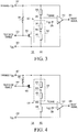
- FIG. 4 is a schematic diagram of a circuit 400 of a second embodiment of the selectable threshold reset circuit 125.
- the circuit 400 includes a comparator 410 that functions similar to comparator 310.
- the circuit 400 has an input terminal 405 for receiving the TEST MODE ENABLE signal and an output terminal 406 for outputting a RESET signal.
- the circuit 400 of includes comparator 410.
- the circuit 400 includes a ladder 420 coupled between a V DD terminal 407 and a V SS terminal 408.
- the ladder 420 comprises resistive elements 431 and 432 in an upper portion 430, and a resistive element in a lower portion 440.
- the circuit 400 includes a switch 450.
- the switch 450 is a PMOS transistor.
- PMOS transistor of the switch 450 is normally off, thereby shorting out resistive element 431 from the upper portion 430 of the ladder 420.
- Circuit 400 of the selectable threshold reset circuit 125 enters the test mode by turning off the PMOS transistor of the switch 450.
- the PMOS transistor requires a low (logical zero) input signal at its gate to turn on.
- the low TEST MODE ENABLE signal causes the PMOS transistor of the switch 450 to turn on, or to conduct, and the circuit 400 of the selectable threshold reset circuit 125 thereby enters the test mode.
- PMOS transistor of the switch 450 When PMOS transistor of the switch 450 is on, it shorts out resistive element 431 from the upper portion 430 of the ladder 420, thereby decreasing the resistance of the upper portion of the ladder.
- the percent of the power supply voltage that is being sampled at node 435 is increased, and the reset threshold is thereby lowered to the test mode reset threshold.
- the circuit 400 includes a pullup resistor 460 coupled between the gate of the PMOS transistor of the switch 450 and the V DD terminal 407.
- the pullup resistor 460 advantageously maintains the PMOS transistor of the switch 450 in an OFF state.
- circuit 400 of the selectable threshold reset circuit 125 does not enter the test mode, and the reset threshold remains at its normal value.
- FIG. 5 is a schematic diagram of a circuit 500 of a third embodiment of the selectable threshold reset circuit 125.
- the circuit 500 includes a comparator 510 that functions similar to comparator 310.
- the circuit 500 has an input terminal 505 for receiving the TEST MODE ENABLE signal and an output terminal 506 for outputting a RESET signal.
- the circuit 500 includes a ladder 520 with one end coupled to a V DD terminal 507.
- the ladder 520 comprises a resistive element in an upper portion 530, and resistive elements 541 and 542 configured parallel to each other, in a lower portion 540.
- the ladder 520 includes a node 535 between the upper portion 530 and the lower portion 540.
- resistive element 542 is coupled to node 535 and the other end of resistive element 542 is coupled to a V SS terminal 508.
- the circuit 500 includes an NMOS transistor as a switch 550.
- One end of resistive element 541 is coupled to node 535 and the other end of resistive element 541 is coupled to a drain of the NMOS transistor.
- the source of the NMOS transistor is coupled to the V SS terminal 508 and the gate of the NMOS transistor is coupled to the input terminal 505.
- the ladder 520 produces a voltage V SENSE at node 535.
- the production tester 102 and 202 causes circuit 500 to receive the active-low TEST MODE ENABLE signal, thereby causing the circuit 500 to enter the test mode.
- the active-low TEST MODE ENABLE signal causes the NMOS transistor of the switch 550 to turn off, or to stop conducting, and the circuit 500 thereby enters the test mode.
- the NMOS transistor requires a high (logical one) input signal at its gate to turn on. When the NMOS transistor is on, it connects resistive element 541 to the V SS terminal 508, thereby reducing the resistance of the lower portion 540 of the ladder 520.
- the NMOS transistor When the circuit 500 is not in the test mode, the NMOS transistor is on, and a certain percent of the power supply voltage is sampled at node 535.
- circuit 500 When circuit 500 is in the test mode, the NMOS transistor is off, and the percent of the power supply voltage that is being sampled at node 535 changes. When NMOS transistor is off, the percent of the power supply voltage that is being sampled at node 535 is increased. By increasing the percent of the power supply voltage that is being sampled at node 535, the reset threshold is lowered to the test mode reset threshold.
- FIG. 6 is a schematic diagram of a circuit 600 of a fourth embodiment of the selectable threshold reset circuit 125.
- the circuit 600 includes a selectable V REF circuit 602 that has an input terminal for receiving the TEST MODE ENABLE signal and an output terminal for outputting a selectable value of V REF to a comparator 610.
- the selectable value of V REF outputted by the selectable V REF circuit 602 to the comparator 610 is based on a bandgap voltage from a reference circuit that is not shown in FIG. 6 .
- the comparator 610 of FIG. 6 is a standard comparator, in contrast to the bandgap comparator 310 of FIGS. 3, 4 and 5 .
- One embodiment of the selectable V REF circuit 602 includes an amplifier circuit (not shown) that has an appropriate gain or attenuation, controlled by the TEST MODE ENABLE signal, using the previous described bandgap voltage reference circuit as a reference, thereby changing the value of V REF inputted into an input terminal 636 of the comparator 610.
- an amplifier circuit not shown
- V REF is inputted into the comparator 610 during normal mode
- another value of V REF is inputted into the comparator during test mode.
- selectable V REF circuit 602 includes second bandgap voltage reference circuit (not shown) that generates a second V REF2 different than V REF , wherein the input terminal 636 of the comparator 610 is multiplexed between V REF and V REF2 .
- the one bandgap voltage reference circuit that generates V REF is used during normal mode, and the second bandgap voltage reference circuit that generates V REF2 is used during test mode, and the multiplexing is controlled by the TEST MODE ENABLE signal.
- Yet another embodiment of the selectable V REF circuit 602 includes a digital-to-analog converter (DAC), wherein the output of the DAC is controlled by the TEST MODE ENABLE signal.
- DAC digital-to-analog converter
- Still another embodiment of the selectable V REF circuit 602 includes a resistor divider network based on either the bandgap reference or the unregulated supply (see FIG. 1 ), but not based on a voltage from the programmable V DD regulator 223, wherein the resistor divider network is controlled by the TEST MODE ENABLE signal.
- the value of V REF inputting into the input terminal 636 of the comparator 610 is decreased, by the selectable V REF circuit 602, in response to the TEST MODE ENABLE signal, from a normal value to a lower value when the selectable threshold reset circuit 125 enters the test mode.
- the low voltage testing system 100 and 200 allows package level, logic operation at a V DD less than a normal voltage without disabling the reset circuit. Also, the low voltage testing system 200 allows package-level logic operation at a V DD less than the normal reset threshold without external pin access to the reset circuit or to V DD . Unlike some known circuits, with the low voltage testing system 100 and 200, during a low voltage test, the selectable threshold reset circuit 125 does not become disabled, and the RESET signal is not inhibited.
- V DD regulator 223 and the selectable threshold reset circuit 125 are controlled in concert by SPI or test mode pins.
- V DD is reduced from its nominal value, for example, 2.5V, to a lower value, for example, 1.75V, as dictated by a fabrication process of the integrated circuit.
- the reset threshold is reduced from its nominal value, e.g., 2.0V, to a lower value, e.g., 1.65V.
- the low voltage testing system 100 and 200 coordinates control of the selectable threshold reset circuit 125 and the programmable V DD regulator 223. During a low voltage test, or scan, the low voltage testing system 100 and 200 synchronizes the reduction of V DD with the lowering of the reset threshold.
- the low voltage testing system 100 and 200 includes local pullup on a control pin to establish a correct start-up start.
- the low voltage testing system 100 and 200 allows a low voltage test to be performed at package level without disabling a reset circuit and without adding pins.
- the selectable threshold reset circuit 125 remains operable even in faulted conditions. In the presence of a fault, e.g., a metal defect in the integrated circuit that causes second line 117, which carries the TEST MODE ENABLE signal, to be always active (logical high), the selectable threshold reset circuit 125 is still functional and operational (although it may be parametrically incorrect), thereby ensuring a proper logic reset during a power-up sequence.
- a fault e.g., a metal defect in the integrated circuit that causes second line 117, which carries the TEST MODE ENABLE signal
- the resistive elements can include three-terminal diffused resistors, two-terminal polysilicon resistors, metal resistors, NiCad resistors, or transistors configured to act as resistors.
- the selectable threshold reset circuit 125 is disposed on an integrated circuit fabricated using a complementary metal oxide semiconductor (CMOS) process. In one embodiment, the selectable threshold reset circuit 125 comprises thin-oxide transistors. In another embodiment, the selectable threshold reset circuit 125 comprises dual gate oxide (DGO) transistors. Although, in one exemplary embodiment, the selectable threshold reset circuit 125 is disposed on an integrated circuit fabricated using CMOS technology, the amplifier circuit can also be disposed on an integrated circuit fabricated using other technologies.
- CMOS complementary metal oxide semiconductor
- DGO dual gate oxide
- selectable threshold reset circuit 125 is disposed on an integrated circuit, the invention is equally usable when constructed entirely of components consisting of discrete devices.
- selectable threshold reset circuit 125 may comprise FETs
- another embodiment of the selectable threshold reset circuit 125 may comprise bipolar junction transistors.
Landscapes
- Engineering & Computer Science (AREA)
- General Engineering & Computer Science (AREA)
- Physics & Mathematics (AREA)
- General Physics & Mathematics (AREA)
- Electronic Switches (AREA)
- Semiconductor Integrated Circuits (AREA)
- Tests Of Electronic Circuits (AREA)
- Testing Of Individual Semiconductor Devices (AREA)
Claims (12)
- Circuit de réinitialisation à seuil sélectionnable (300) couplé à une première borne d'alimentation (VDD) et à une seconde borne d'alimentation (VSS), comprenant :un circuit diviseur de tension (320) couplé à la première borne d'alimentation (VDD) et à la seconde borne d'alimentation (VSS), destiné à générer une tension VSENSE qui représente une fraction de la tension à la première borne d'alimentation,un comparateur (310) possédant une première borne d'entrée (335) couplée à la tension VSENSE générée par le circuit diviseur de tension, une seconde borne d'entrée (336) couplée à une tension de référence (VREF), ainsi qu'une borne de sortie (306) destinée à délivrer un signal RESET de réinitialisation lorsque la première borne d'alimentation (VDD) se trouve à une tension inférieure ou égale à une tension de seuil de réinitialisation du circuit de réinitialisation à seuil sélectionnable, etun interrupteur (350) destiné à commander le circuit diviseur de tension, l'interrupteur comportant une première borne d'interrupteur couplée au circuit diviseur de tension, une seconde borne d'interrupteur couplée à la seconde borne d'alimentation (VSS) et une borne d'entrée destinée à activer l'interrupteur de sorte que :lorsque l'interrupteur (350) se trouve dans un premier état et que la première borne d'alimentation (VDD) se trouve à un niveau normal de tension d'alimentation, le signal RESET est délivré à une tension normale de seuil de réinitialisation, etlorsque l'interrupteur (350) se trouve dans un second état et que la première borne d'alimentation (VDD) se trouve au niveau de tension de mode de test qui est inférieur au niveau normal de tension d'alimentation, le signal RESET est délivré à une tension de seuil de réinitialisation de mode de test qui est inférieure à la tension normale de seuil de réinitialisation,caractérisé parune résistance de rappel au niveau haut (360) couplée entre la borne d'entrée de l'interrupteur (350) et la première borne d'alimentation de sorte à ce que la tension de seuil de réinitialisation reste à la tension normale de seuil de réinitialisation en l'absence d'un signal à la borne d'entrée de l'interrupteur.
- Circuit de réinitialisation à seuil sélectionnable (300) selon la revendication 1, dans lequel le comparateur (310) compare la tension VSENSE à la tension de référence, et dans lequel la tension VSENSE est plus importante lorsque l'interrupteur (350) se trouve dans le premier état que dans le second état.
- Circuit de réinitialisation à seuil sélectionnable (300) selon la revendication 2, le circuit de réinitialisation à seuil sélectionnable étant couplé à un circuit en test, le circuit en test étant couplé à l'alimentation, et dans lequel le niveau de tension de l'alimentation est réduit lorsque l'interrupteur est activé pour se trouver dans le second état.
- Circuit de réinitialisation à seuil sélectionnable (300) selon la revendication 3, dans lequel le circuit diviseur de tension est un circuit en échelle diviseur de tension (320) qui inclut :une première partie (330) couplée entre la première borne d'entrée du comparateur et la première borne d'alimentation, etune seconde partie (340) couplée entre la première borne d'entrée du comparateur et la seconde borne d'alimentation,dans lequel le circuit en échelle diviseur de tension génère la tension VSENSE au niveau d'un nœud (335, 435 et 535) entre la première partie et la seconde partie.
- Circuit de réinitialisation à seuil sélectionnable (300) selon la revendication 4, dans lequel la seconde partie (340) du circuit en échelle diviseur de tension inclut :une première résistance (341) couplée entre la première borne d'entrée du comparateur et un nœud intermédiaire (343) de la seconde partie, etune seconde résistance (342) couplée entre le nœud intermédiaire de la seconde partie et la seconde borne d'alimentation, etdans lequel la première borne d'interrupteur est couplée au nœud intermédiaire de la seconde partie.
- Circuit de réinitialisation à seuil sélectionnable (300) selon la revendication 4, dans lequel l'interrupteur (350) commande la topologie du circuit en échelle diviseur de tension, l'interrupteur comportant une première borne d'interrupteur couplée à la seconde partie, une seconde borne d'interrupteur couplée à la seconde borne d'alimentation et une borne d'entrée destinée à activer l'interrupteur, de sorte que :lorsque l'interrupteur est fermé et que la première borne d'alimentation se trouve à au niveau normal de tension d'alimentation, le signal RESET est délivré à une tension normale de seuil de réinitialisation, etlorsque l'interrupteur est ouvert et que la première borne d'alimentation se trouve à un niveau de tension d'alimentation de mode de test qui est inférieur au niveau normal de tension d'alimentation, le signal RESET est délivré à une tension de seuil de réinitialisation de mode de test qui est inférieure à la tension normale de seuil de réinitialisation.
- Circuit de réinitialisation à seuil sélectionnable (300) selon la revendication 6, dans lequel le rapport entre la tension de seuil de réinitialisation de mode de test et la tension normale de seuil de réinitialisation est proportionnel à un seuil situé entre le niveau de tension d'alimentation de mode de test y et le niveau normal de tension d'alimentation.
- Circuit de réinitialisation à seuil sélectionnable (300) selon la revendication 5, dans lequel le niveau de tension de la première borne d'alimentation est réduit à une valeur inférieure au niveau normal de tension d'alimentation après la fermeture de l'interrupteur.
- Circuit de réinitialisation à seuil sélectionnable (300) selon la revendication 1, dans lequel la tension de seuil de réinitialisation reste au niveau normal de tension de seuil de réinitialisation en l'absence d'un signal bas TEST MODE ENABLE (activation du mode de test) sur la borne d'entrée de l'interrupteur.
- Procédé de réalisation d'un test à basse tension d'un circuit à l'intérieur de l'outil de circuit intégré (104 et 204), comprenant :le positionnement de l'alimentation d'un circuit en test et celui d'un circuit de réinitialisation à un niveau normal de tension d'alimentation, le circuit en test et le circuit de réinitialisation se trouvant à l'intérieur d'un boîtier de circuit intégré, le circuit de réinitialisation comportant une borne d'entrée destinée à recevoir un signal TEST MODE ENABLE, ainsi qu'une résistance de rappel au niveau haut couplée entre l'alimentation et la borne d'entrée, le circuit de réinitialisation délivrant en sortie un signal RESET au circuit en test lorsque le niveau de tension de l'alimentation se trouve à une tension de seuil de réinitialisation, et la tension de seuil de réinitialisation du circuit de réinitialisation pouvant être sélectionnée à un niveau parmi une tension normale de seuil de réinitialisation et une tension de seuil de réinitialisation de mode de test, en fonction de la valeur du signal TEST MODE ENABLE,la délivrance du signal TEST MODE ENABLE au circuit de réinitialisation de sorte à ce que la valeur du signal TEST MODE ENABLE amène le circuit de réinitialisation à délivrer le signal RESET au circuit en test lorsque le niveau de tension de l'alimentation se trouve au seuil de réinitialisation de mode de test ou en dessous de celui-ci,la réduction du niveau de tension de l'alimentation du circuit de réinitialisation et du circuit en test à un niveau de tension d'alimentation de mode de test, le niveau de tension d'alimentation de mode de test étant inférieur au niveau normal de tension d'alimentation du circuit de réinitialisation, etla détermination du fonctionnement du circuit en test lorsque le niveau de tension de l'alimentation du circuit en test se trouve au niveau de tension d'alimentation de mode de test,dans lequel la tension de seuil de réinitialisation reste à la tension normale de seuil de réinitialisation sur la base d'une tension au travers de la résistance de rappel au niveau haut depuis la tension de l'alimentation en l'absence d'un signal à la borne d'entrée du circuit de réinitialisation.
- Procédé selon la revendication 9, dans lequel le rapport entre la tension de seuil de réinitialisation de mode de test et la tension normale de seuil de réinitialisation est proportionnel au rapport entre le niveau de tension de mode de test d'alimentation et le niveau de tension normale d'alimentation.
- Procédé selon les revendications 10 ou 11, dans lequel la délivrance du signal TEST MODE ENABLE au circuit de réinitialisation et au circuit en test se produit simultanément avec la réduction du niveau de tension d'alimentation du circuit en test au niveau de tension d'alimentation de mode de test.
Applications Claiming Priority (1)
| Application Number | Priority Date | Filing Date | Title |
|---|---|---|---|
| US13/071,025 US8531194B2 (en) | 2011-03-24 | 2011-03-24 | Selectable threshold reset circuit |
Related Parent Applications (2)
| Application Number | Title | Priority Date | Filing Date |
|---|---|---|---|
| US13/071,025 Previously-Filed-Application US8531194B2 (en) | 2011-03-24 | 2011-03-24 | Selectable threshold reset circuit |
| US201113071025 Previously-Filed-Application | 2011-03-24 |
Publications (3)
| Publication Number | Publication Date |
|---|---|
| EP2503346A2 EP2503346A2 (fr) | 2012-09-26 |
| EP2503346A3 EP2503346A3 (fr) | 2013-11-20 |
| EP2503346B1 true EP2503346B1 (fr) | 2020-08-05 |
Family
ID=46027568
Family Applications (1)
| Application Number | Title | Priority Date | Filing Date |
|---|---|---|---|
| EP12160380.7A Active EP2503346B1 (fr) | 2011-03-24 | 2012-03-20 | Circuit de réinitialisation ayant un seuil sélectionnable |
Country Status (4)
| Country | Link |
|---|---|
| US (1) | US8531194B2 (fr) |
| EP (1) | EP2503346B1 (fr) |
| JP (1) | JP6095199B2 (fr) |
| CN (1) | CN102692596B (fr) |
Families Citing this family (32)
| Publication number | Priority date | Publication date | Assignee | Title |
|---|---|---|---|---|
| US9086434B1 (en) * | 2011-12-06 | 2015-07-21 | Altera Corporation | Methods and systems for voltage reference power detection |
| US10284073B2 (en) * | 2012-04-25 | 2019-05-07 | Hamilton Sundstrand Corporation | Power supply built-in testing |
| US9013202B2 (en) * | 2012-05-23 | 2015-04-21 | International Business Machines Corporation | Testing structure and method of using the testing structure |
| US8742805B2 (en) * | 2012-07-26 | 2014-06-03 | Samsung Electro-Mechanics Co., Ltd. | Power on reset device and power on reset method |
| US8928372B2 (en) * | 2013-03-08 | 2015-01-06 | Taiwan Semiconductor Manufacturing Company, Ltd. | Multiple power domain electronic device and related method |
| TW201504648A (zh) * | 2013-07-25 | 2015-02-01 | Terminus Technology Inc | 利用僅既有的功能腳位實現通信介面的晶片 |
| US9506979B2 (en) | 2014-04-02 | 2016-11-29 | Freescale Semiconductor, Inc. | Test mode entry interlock |
| US9606563B2 (en) | 2014-04-08 | 2017-03-28 | Texas Instruments Deutschland Gmbh | Bandgap reference voltage failure detection |
| US9377804B2 (en) * | 2014-04-10 | 2016-06-28 | Qualcomm Incorporated | Switchable package capacitor for charge conservation and series resistance |
| US9312850B2 (en) | 2014-08-20 | 2016-04-12 | Freescale Semiconductor, Inc. | Testable power-on-reset circuit |
| US9634653B2 (en) * | 2014-12-11 | 2017-04-25 | Texas Instruments Incorporated | Method and apparatus for a brown out detector |
| CN104490478A (zh) * | 2015-01-09 | 2015-04-08 | 王小楠 | 医用射线定位薄膜及定位便捷的病变处拍照方法 |
| KR20180039069A (ko) * | 2015-08-11 | 2018-04-17 | 콘티넨탈 테베스 아게 운트 코. 오하게 | 측정 변수를 측정하기 위한 디바이스 |
| DE102015215331A1 (de) | 2015-08-11 | 2017-02-16 | Continental Teves Ag & Co. Ohg | Elektronische Steuerungseinheit |
| CN105141119B (zh) * | 2015-10-10 | 2018-01-05 | 上海灿瑞科技股份有限公司 | 一种上电清零和欠压锁定启动电路 |
| KR20170071828A (ko) * | 2015-12-16 | 2017-06-26 | 에스케이하이닉스 주식회사 | 반도체 장치 및 이를 포함하는 테스트 시스템 |
| JP2017143448A (ja) * | 2016-02-11 | 2017-08-17 | アルパイン株式会社 | リセット信号発生回路 |
| DE102016202403A1 (de) | 2016-02-17 | 2017-08-17 | Continental Teves Ag & Co. Ohg | Sensor |
| DE102016202402A1 (de) | 2016-02-17 | 2017-08-17 | Continental Teves Ag & Co. Ohg | Sensor |
| US10228415B1 (en) * | 2016-09-27 | 2019-03-12 | Altera Corporation | Apparatus and method for security in an integrated circuit |
| US10050618B1 (en) | 2017-04-13 | 2018-08-14 | Nxp Usa, Inc. | Reset management circuit and method therefor |
| EP3451338B1 (fr) * | 2017-08-30 | 2020-10-07 | Nxp B.V. | Circuit indicateur prêt à l'alimentation |
| US10620267B2 (en) * | 2017-09-20 | 2020-04-14 | Stmicroelectronics International N.V. | Circuitry for testing non-maskable voltage monitor for power management block |
| US10317921B1 (en) * | 2018-04-13 | 2019-06-11 | Nxp Usa, Inc. | Effective clamping in power supplies |
| JP6746659B2 (ja) * | 2018-11-09 | 2020-08-26 | 華邦電子股▲ふん▼有限公司Winbond Electronics Corp. | メモリデバイス及びその内蔵セルフテスト方法 |
| US10979044B2 (en) * | 2019-03-14 | 2021-04-13 | Infineon Technologies Ag | Chip reset via communication interface terminals |
| CN111157877B (zh) * | 2019-12-31 | 2022-04-15 | 西安翔腾微电子科技有限公司 | 一种关态负载断路检测电路 |
| JP7413082B2 (ja) * | 2020-03-02 | 2024-01-15 | メイコーエンベデッドプロダクツ株式会社 | 監視電圧閾値切替回路、リセット監視システム、制御信号生成回路が行う処理方法及びプログラム |
| CN111755035A (zh) * | 2020-06-03 | 2020-10-09 | 深圳金茂电子有限公司 | 一种电源芯片管理系统及方法 |
| TWI764168B (zh) * | 2020-06-05 | 2022-05-11 | 大陸商北京集創北方科技股份有限公司 | 欠電壓檢測電路及利用其之控制器和電子設備 |
| CN112986800B (zh) * | 2021-02-19 | 2024-04-09 | 宏晶微电子科技股份有限公司 | Por电路测试方法及装置 |
| CN113315498B (zh) * | 2021-05-27 | 2022-08-23 | 北京中电华大电子设计有限责任公司 | 一种高精度por电路 |
Citations (1)
| Publication number | Priority date | Publication date | Assignee | Title |
|---|---|---|---|---|
| WO2009066575A1 (fr) * | 2007-11-19 | 2009-05-28 | Sharp Kabushiki Kaisha | Circuit de réinitialisation à la mise sous tension et carte ci de type à combinaison |
Family Cites Families (26)
| Publication number | Priority date | Publication date | Assignee | Title |
|---|---|---|---|---|
| US5103113A (en) | 1990-06-13 | 1992-04-07 | Texas Instruments Incorporated | Driving circuit for providing a voltage boasted over the power supply voltage source as a driving signal |
| US5115146A (en) | 1990-08-17 | 1992-05-19 | Sgs-Thomson Microelectronics, Inc. | Power-on reset circuit for controlling test mode entry |
| US5181203A (en) | 1990-12-21 | 1993-01-19 | Vlsi Technology, Inc. | Testable power-on-reset circuit |
| US5149987A (en) | 1991-08-19 | 1992-09-22 | Vlsi Technology, Inc. | Provision of circuit reset without a dedicated I/O pin |
| JPH05259859A (ja) | 1992-02-28 | 1993-10-08 | Oki Lsi Tekunoroji Kansai:Kk | オート・クリヤー回路 |
| US5394104A (en) | 1992-06-25 | 1995-02-28 | Xilinx, Inc. | Power-on reset circuit including dual sense amplifiers |
| US5450417A (en) | 1993-10-26 | 1995-09-12 | Texas Instruments Incorporated | Circuit for testing power-on-reset circuitry |
| US5991887A (en) | 1996-02-28 | 1999-11-23 | Dallas Semiconductor Corporation | Low power wake up circuitry, with internal power down of the wake up circuitry itself |
| JPH10105255A (ja) * | 1996-09-25 | 1998-04-24 | Toshiba Microelectron Corp | 低電圧検知回路 |
| JPH10207580A (ja) * | 1997-01-17 | 1998-08-07 | Hitachi Ltd | パワーオンリセット発生回路および半導体集積回路並びにicカード |
| US5912562A (en) * | 1997-02-04 | 1999-06-15 | Motorola Inc. | Quiescent current monitor circuit for wafer level integrated circuit testing |
| JP3288249B2 (ja) | 1997-03-31 | 2002-06-04 | 東芝マイクロエレクトロニクス株式会社 | パワーオンリセット回路 |
| US6073263A (en) | 1997-10-29 | 2000-06-06 | Credence Systems Corporation | Parallel processing pattern generation system for an integrated circuit tester |
| US6188257B1 (en) | 1999-02-01 | 2001-02-13 | Vlsi Technology, Inc. | Power-on-reset logic with secure power down capability |
| US6618312B2 (en) | 2001-05-04 | 2003-09-09 | Texas Instruments Incorporated | Method and device for providing a multiple phase power on reset |
| JP2003059297A (ja) * | 2001-08-08 | 2003-02-28 | Mitsubishi Electric Corp | 半導体記憶装置およびそれを用いた半導体モジュール |
| US7057427B2 (en) | 2004-07-15 | 2006-06-06 | Freescale Semiconductor, Inc | Power on reset circuit |
| ITSV20040035A1 (it) * | 2004-09-29 | 2004-12-29 | Alstom Ferroviaria Spa | Circuito di controllo dell'alimentazione di circuiti elettronici in particolare di circuiti elettronici di elaborazione ed in special modo di circuiti di elaborazione aventi una struttura del tipo con architettura due su due |
| US7142024B2 (en) | 2004-11-01 | 2006-11-28 | Stmicroelectronics, Inc. | Power on reset circuit |
| US7265595B1 (en) | 2006-03-03 | 2007-09-04 | Cypress Semiconductor Corporation | Stochastic reset circuit |
| US7710105B2 (en) | 2006-03-14 | 2010-05-04 | Atmel Corporation | Circuit reset testing methods |
| US7519486B2 (en) | 2006-03-31 | 2009-04-14 | Atmel Corporation | Method and apparatus to test the power-on-reset trip point of an integrated circuit |
| US7711971B1 (en) | 2006-06-28 | 2010-05-04 | Linear Technology Corporation | Multi-input power supply supervisor |
| US7589568B2 (en) * | 2007-05-04 | 2009-09-15 | Microchip Technology Incorporated | Variable power and response time brown-out-reset circuit |
| JP5133804B2 (ja) * | 2008-07-18 | 2013-01-30 | ルネサスエレクトロニクス株式会社 | リセット信号生成回路 |
| CN101980445B (zh) * | 2010-11-16 | 2012-08-08 | 成都国腾电子技术股份有限公司 | 高可靠零功耗复位电路 |
-
2011
- 2011-03-24 US US13/071,025 patent/US8531194B2/en active Active
-
2012
- 2012-03-20 EP EP12160380.7A patent/EP2503346B1/fr active Active
- 2012-03-23 JP JP2012067874A patent/JP6095199B2/ja active Active
- 2012-03-23 CN CN201210079180.8A patent/CN102692596B/zh active Active
Patent Citations (1)
| Publication number | Priority date | Publication date | Assignee | Title |
|---|---|---|---|---|
| WO2009066575A1 (fr) * | 2007-11-19 | 2009-05-28 | Sharp Kabushiki Kaisha | Circuit de réinitialisation à la mise sous tension et carte ci de type à combinaison |
Also Published As
| Publication number | Publication date |
|---|---|
| JP2012205310A (ja) | 2012-10-22 |
| US20120242380A1 (en) | 2012-09-27 |
| CN102692596A (zh) | 2012-09-26 |
| US8531194B2 (en) | 2013-09-10 |
| EP2503346A2 (fr) | 2012-09-26 |
| CN102692596B (zh) | 2016-12-14 |
| EP2503346A3 (fr) | 2013-11-20 |
| JP6095199B2 (ja) | 2017-03-15 |
Similar Documents
| Publication | Publication Date | Title |
|---|---|---|
| EP2503346B1 (fr) | Circuit de réinitialisation ayant un seuil sélectionnable | |
| US7639052B2 (en) | Power-on-reset circuitry | |
| KR970008141B1 (ko) | 반도체장치의 번인회로 | |
| JP6239106B2 (ja) | 電源電圧よりも大きい電圧を支持するスイッチ | |
| TWI900198B (zh) | 攻擊偵測電路和攻擊偵測方法 | |
| EP0600527A1 (fr) | Circuit de test à charge élevée pour un circuit integré avec convertisseur d'abaisseur de tension sur puce | |
| US8988117B2 (en) | Gate-stress test circuit without test pad | |
| US9312850B2 (en) | Testable power-on-reset circuit | |
| US8525555B2 (en) | Power detector | |
| CN101971488B (zh) | 具有过压保护的差分电流输出驱动器 | |
| KR100455442B1 (ko) | 저전압 검출기 | |
| KR101442859B1 (ko) | 전력 관리 회로 및 방법 | |
| US8446163B2 (en) | Test circuit and test method for testing differential input circuit | |
| EP3239800B1 (fr) | Dispositif électronique | |
| CN111585552A (zh) | 输出驱动器电路 | |
| JP2013110326A (ja) | トリミング回路及び調整回路 | |
| US20030071661A1 (en) | Input circuit | |
| EP1989780B1 (fr) | Circuit intégré | |
| US7825704B2 (en) | Threshold personalization testmode | |
| JP4855913B2 (ja) | ボルテージレギュレータ | |
| CN113114195B (zh) | 一种断电关闭电路、断电关闭芯片及开关芯片 | |
| US11063588B1 (en) | Reset device, circuit device, and resetting method | |
| JP3085806B2 (ja) | Cmos型半導体集積回路装置 | |
| US11469586B2 (en) | Over-current protection circuit | |
| US20080297224A1 (en) | Minimizing Static Current Consumption While Providing Higher-Swing Output Signals when Components of an Integrated Circuit are Fabricated using a Lower-Voltage Process |
Legal Events
| Date | Code | Title | Description |
|---|---|---|---|
| PUAI | Public reference made under article 153(3) epc to a published international application that has entered the european phase |
Free format text: ORIGINAL CODE: 0009012 |
|
| AK | Designated contracting states |
Kind code of ref document: A2 Designated state(s): AL AT BE BG CH CY CZ DE DK EE ES FI FR GB GR HR HU IE IS IT LI LT LU LV MC MK MT NL NO PL PT RO RS SE SI SK SM TR |
|
| AX | Request for extension of the european patent |
Extension state: BA ME |
|
| PUAL | Search report despatched |
Free format text: ORIGINAL CODE: 0009013 |
|
| AK | Designated contracting states |
Kind code of ref document: A3 Designated state(s): AL AT BE BG CH CY CZ DE DK EE ES FI FR GB GR HR HU IE IS IT LI LT LU LV MC MK MT NL NO PL PT RO RS SE SI SK SM TR |
|
| AX | Request for extension of the european patent |
Extension state: BA ME |
|
| RIC1 | Information provided on ipc code assigned before grant |
Ipc: G01R 31/30 20060101AFI20131014BHEP |
|
| 17P | Request for examination filed |
Effective date: 20140520 |
|
| RBV | Designated contracting states (corrected) |
Designated state(s): AL AT BE BG CH CY CZ DE DK EE ES FI FR GB GR HR HU IE IS IT LI LT LU LV MC MK MT NL NO PL PT RO RS SE SI SK SM TR |
|
| RAP1 | Party data changed (applicant data changed or rights of an application transferred) |
Owner name: NXP USA, INC. |
|
| STAA | Information on the status of an ep patent application or granted ep patent |
Free format text: STATUS: EXAMINATION IS IN PROGRESS |
|
| 17Q | First examination report despatched |
Effective date: 20180718 |
|
| GRAP | Despatch of communication of intention to grant a patent |
Free format text: ORIGINAL CODE: EPIDOSNIGR1 |
|
| STAA | Information on the status of an ep patent application or granted ep patent |
Free format text: STATUS: GRANT OF PATENT IS INTENDED |
|
| INTG | Intention to grant announced |
Effective date: 20200506 |
|
| GRAS | Grant fee paid |
Free format text: ORIGINAL CODE: EPIDOSNIGR3 |
|
| GRAA | (expected) grant |
Free format text: ORIGINAL CODE: 0009210 |
|
| STAA | Information on the status of an ep patent application or granted ep patent |
Free format text: STATUS: THE PATENT HAS BEEN GRANTED |
|
| AK | Designated contracting states |
Kind code of ref document: B1 Designated state(s): AL AT BE BG CH CY CZ DE DK EE ES FI FR GB GR HR HU IE IS IT LI LT LU LV MC MK MT NL NO PL PT RO RS SE SI SK SM TR |
|
| REG | Reference to a national code |
Ref country code: GB Ref legal event code: FG4D |
|
| REG | Reference to a national code |
Ref country code: CH Ref legal event code: EP |
|
| REG | Reference to a national code |
Ref country code: AT Ref legal event code: REF Ref document number: 1299460 Country of ref document: AT Kind code of ref document: T Effective date: 20200815 |
|
| REG | Reference to a national code |
Ref country code: DE Ref legal event code: R096 Ref document number: 602012071583 Country of ref document: DE |
|
| REG | Reference to a national code |
Ref country code: IE Ref legal event code: FG4D |
|
| REG | Reference to a national code |
Ref country code: LT Ref legal event code: MG4D |
|
| REG | Reference to a national code |
Ref country code: NL Ref legal event code: MP Effective date: 20200805 |
|
| REG | Reference to a national code |
Ref country code: AT Ref legal event code: MK05 Ref document number: 1299460 Country of ref document: AT Kind code of ref document: T Effective date: 20200805 |
|
| PG25 | Lapsed in a contracting state [announced via postgrant information from national office to epo] |
Ref country code: FI Free format text: LAPSE BECAUSE OF FAILURE TO SUBMIT A TRANSLATION OF THE DESCRIPTION OR TO PAY THE FEE WITHIN THE PRESCRIBED TIME-LIMIT Effective date: 20200805 Ref country code: PT Free format text: LAPSE BECAUSE OF FAILURE TO SUBMIT A TRANSLATION OF THE DESCRIPTION OR TO PAY THE FEE WITHIN THE PRESCRIBED TIME-LIMIT Effective date: 20201207 Ref country code: SE Free format text: LAPSE BECAUSE OF FAILURE TO SUBMIT A TRANSLATION OF THE DESCRIPTION OR TO PAY THE FEE WITHIN THE PRESCRIBED TIME-LIMIT Effective date: 20200805 Ref country code: LT Free format text: LAPSE BECAUSE OF FAILURE TO SUBMIT A TRANSLATION OF THE DESCRIPTION OR TO PAY THE FEE WITHIN THE PRESCRIBED TIME-LIMIT Effective date: 20200805 Ref country code: AT Free format text: LAPSE BECAUSE OF FAILURE TO SUBMIT A TRANSLATION OF THE DESCRIPTION OR TO PAY THE FEE WITHIN THE PRESCRIBED TIME-LIMIT Effective date: 20200805 Ref country code: HR Free format text: LAPSE BECAUSE OF FAILURE TO SUBMIT A TRANSLATION OF THE DESCRIPTION OR TO PAY THE FEE WITHIN THE PRESCRIBED TIME-LIMIT Effective date: 20200805 Ref country code: GR Free format text: LAPSE BECAUSE OF FAILURE TO SUBMIT A TRANSLATION OF THE DESCRIPTION OR TO PAY THE FEE WITHIN THE PRESCRIBED TIME-LIMIT Effective date: 20201106 Ref country code: ES Free format text: LAPSE BECAUSE OF FAILURE TO SUBMIT A TRANSLATION OF THE DESCRIPTION OR TO PAY THE FEE WITHIN THE PRESCRIBED TIME-LIMIT Effective date: 20200805 Ref country code: NO Free format text: LAPSE BECAUSE OF FAILURE TO SUBMIT A TRANSLATION OF THE DESCRIPTION OR TO PAY THE FEE WITHIN THE PRESCRIBED TIME-LIMIT Effective date: 20201105 Ref country code: BG Free format text: LAPSE BECAUSE OF FAILURE TO SUBMIT A TRANSLATION OF THE DESCRIPTION OR TO PAY THE FEE WITHIN THE PRESCRIBED TIME-LIMIT Effective date: 20201105 |
|
| PG25 | Lapsed in a contracting state [announced via postgrant information from national office to epo] |
Ref country code: NL Free format text: LAPSE BECAUSE OF FAILURE TO SUBMIT A TRANSLATION OF THE DESCRIPTION OR TO PAY THE FEE WITHIN THE PRESCRIBED TIME-LIMIT Effective date: 20200805 Ref country code: LV Free format text: LAPSE BECAUSE OF FAILURE TO SUBMIT A TRANSLATION OF THE DESCRIPTION OR TO PAY THE FEE WITHIN THE PRESCRIBED TIME-LIMIT Effective date: 20200805 Ref country code: RS Free format text: LAPSE BECAUSE OF FAILURE TO SUBMIT A TRANSLATION OF THE DESCRIPTION OR TO PAY THE FEE WITHIN THE PRESCRIBED TIME-LIMIT Effective date: 20200805 Ref country code: PL Free format text: LAPSE BECAUSE OF FAILURE TO SUBMIT A TRANSLATION OF THE DESCRIPTION OR TO PAY THE FEE WITHIN THE PRESCRIBED TIME-LIMIT Effective date: 20200805 Ref country code: IS Free format text: LAPSE BECAUSE OF FAILURE TO SUBMIT A TRANSLATION OF THE DESCRIPTION OR TO PAY THE FEE WITHIN THE PRESCRIBED TIME-LIMIT Effective date: 20201205 |
|
| PG25 | Lapsed in a contracting state [announced via postgrant information from national office to epo] |
Ref country code: DK Free format text: LAPSE BECAUSE OF FAILURE TO SUBMIT A TRANSLATION OF THE DESCRIPTION OR TO PAY THE FEE WITHIN THE PRESCRIBED TIME-LIMIT Effective date: 20200805 Ref country code: CZ Free format text: LAPSE BECAUSE OF FAILURE TO SUBMIT A TRANSLATION OF THE DESCRIPTION OR TO PAY THE FEE WITHIN THE PRESCRIBED TIME-LIMIT Effective date: 20200805 Ref country code: EE Free format text: LAPSE BECAUSE OF FAILURE TO SUBMIT A TRANSLATION OF THE DESCRIPTION OR TO PAY THE FEE WITHIN THE PRESCRIBED TIME-LIMIT Effective date: 20200805 Ref country code: RO Free format text: LAPSE BECAUSE OF FAILURE TO SUBMIT A TRANSLATION OF THE DESCRIPTION OR TO PAY THE FEE WITHIN THE PRESCRIBED TIME-LIMIT Effective date: 20200805 Ref country code: SM Free format text: LAPSE BECAUSE OF FAILURE TO SUBMIT A TRANSLATION OF THE DESCRIPTION OR TO PAY THE FEE WITHIN THE PRESCRIBED TIME-LIMIT Effective date: 20200805 |
|
| REG | Reference to a national code |
Ref country code: DE Ref legal event code: R097 Ref document number: 602012071583 Country of ref document: DE |
|
| PG25 | Lapsed in a contracting state [announced via postgrant information from national office to epo] |
Ref country code: AL Free format text: LAPSE BECAUSE OF FAILURE TO SUBMIT A TRANSLATION OF THE DESCRIPTION OR TO PAY THE FEE WITHIN THE PRESCRIBED TIME-LIMIT Effective date: 20200805 |
|
| PLBE | No opposition filed within time limit |
Free format text: ORIGINAL CODE: 0009261 |
|
| STAA | Information on the status of an ep patent application or granted ep patent |
Free format text: STATUS: NO OPPOSITION FILED WITHIN TIME LIMIT |
|
| PG25 | Lapsed in a contracting state [announced via postgrant information from national office to epo] |
Ref country code: SK Free format text: LAPSE BECAUSE OF FAILURE TO SUBMIT A TRANSLATION OF THE DESCRIPTION OR TO PAY THE FEE WITHIN THE PRESCRIBED TIME-LIMIT Effective date: 20200805 |
|
| 26N | No opposition filed |
Effective date: 20210507 |
|
| PG25 | Lapsed in a contracting state [announced via postgrant information from national office to epo] |
Ref country code: IT Free format text: LAPSE BECAUSE OF FAILURE TO SUBMIT A TRANSLATION OF THE DESCRIPTION OR TO PAY THE FEE WITHIN THE PRESCRIBED TIME-LIMIT Effective date: 20200805 |
|
| PG25 | Lapsed in a contracting state [announced via postgrant information from national office to epo] |
Ref country code: SI Free format text: LAPSE BECAUSE OF FAILURE TO SUBMIT A TRANSLATION OF THE DESCRIPTION OR TO PAY THE FEE WITHIN THE PRESCRIBED TIME-LIMIT Effective date: 20200805 |
|
| PG25 | Lapsed in a contracting state [announced via postgrant information from national office to epo] |
Ref country code: MC Free format text: LAPSE BECAUSE OF FAILURE TO SUBMIT A TRANSLATION OF THE DESCRIPTION OR TO PAY THE FEE WITHIN THE PRESCRIBED TIME-LIMIT Effective date: 20200805 |
|
| REG | Reference to a national code |
Ref country code: CH Ref legal event code: PL |
|
| GBPC | Gb: european patent ceased through non-payment of renewal fee |
Effective date: 20210320 |
|
| REG | Reference to a national code |
Ref country code: BE Ref legal event code: MM Effective date: 20210331 |
|
| PG25 | Lapsed in a contracting state [announced via postgrant information from national office to epo] |
Ref country code: CH Free format text: LAPSE BECAUSE OF NON-PAYMENT OF DUE FEES Effective date: 20210331 Ref country code: LU Free format text: LAPSE BECAUSE OF NON-PAYMENT OF DUE FEES Effective date: 20210320 Ref country code: LI Free format text: LAPSE BECAUSE OF NON-PAYMENT OF DUE FEES Effective date: 20210331 Ref country code: IE Free format text: LAPSE BECAUSE OF NON-PAYMENT OF DUE FEES Effective date: 20210320 Ref country code: FR Free format text: LAPSE BECAUSE OF NON-PAYMENT OF DUE FEES Effective date: 20210331 Ref country code: GB Free format text: LAPSE BECAUSE OF NON-PAYMENT OF DUE FEES Effective date: 20210320 |
|
| PG25 | Lapsed in a contracting state [announced via postgrant information from national office to epo] |
Ref country code: BE Free format text: LAPSE BECAUSE OF NON-PAYMENT OF DUE FEES Effective date: 20210331 |
|
| PG25 | Lapsed in a contracting state [announced via postgrant information from national office to epo] |
Ref country code: HU Free format text: LAPSE BECAUSE OF FAILURE TO SUBMIT A TRANSLATION OF THE DESCRIPTION OR TO PAY THE FEE WITHIN THE PRESCRIBED TIME-LIMIT; INVALID AB INITIO Effective date: 20120320 Ref country code: CY Free format text: LAPSE BECAUSE OF FAILURE TO SUBMIT A TRANSLATION OF THE DESCRIPTION OR TO PAY THE FEE WITHIN THE PRESCRIBED TIME-LIMIT Effective date: 20200805 |
|
| P01 | Opt-out of the competence of the unified patent court (upc) registered |
Effective date: 20230725 |
|
| PG25 | Lapsed in a contracting state [announced via postgrant information from national office to epo] |
Ref country code: MK Free format text: LAPSE BECAUSE OF FAILURE TO SUBMIT A TRANSLATION OF THE DESCRIPTION OR TO PAY THE FEE WITHIN THE PRESCRIBED TIME-LIMIT Effective date: 20200805 |
|
| PG25 | Lapsed in a contracting state [announced via postgrant information from national office to epo] |
Ref country code: MT Free format text: LAPSE BECAUSE OF FAILURE TO SUBMIT A TRANSLATION OF THE DESCRIPTION OR TO PAY THE FEE WITHIN THE PRESCRIBED TIME-LIMIT Effective date: 20200805 |
|
| PG25 | Lapsed in a contracting state [announced via postgrant information from national office to epo] |
Ref country code: TR Free format text: LAPSE BECAUSE OF FAILURE TO SUBMIT A TRANSLATION OF THE DESCRIPTION OR TO PAY THE FEE WITHIN THE PRESCRIBED TIME-LIMIT Effective date: 20200805 |
|
| PGFP | Annual fee paid to national office [announced via postgrant information from national office to epo] |
Ref country code: DE Payment date: 20260219 Year of fee payment: 15 |