EP2528093A1 - Halbleiterbauelement, festkörperabbildungsvorrichtung und kamerasystem - Google Patents
Halbleiterbauelement, festkörperabbildungsvorrichtung und kamerasystem Download PDFInfo
- Publication number
- EP2528093A1 EP2528093A1 EP10842233A EP10842233A EP2528093A1 EP 2528093 A1 EP2528093 A1 EP 2528093A1 EP 10842233 A EP10842233 A EP 10842233A EP 10842233 A EP10842233 A EP 10842233A EP 2528093 A1 EP2528093 A1 EP 2528093A1
- Authority
- EP
- European Patent Office
- Prior art keywords
- chip
- circuit
- power supply
- wiring
- image sensor
- Prior art date
- Legal status (The legal status is an assumption and is not a legal conclusion. Google has not performed a legal analysis and makes no representation as to the accuracy of the status listed.)
- Granted
Links
Images






Classifications
-
- H—ELECTRICITY
- H10—SEMICONDUCTOR DEVICES; ELECTRIC SOLID-STATE DEVICES NOT OTHERWISE PROVIDED FOR
- H10F—INORGANIC SEMICONDUCTOR DEVICES SENSITIVE TO INFRARED RADIATION, LIGHT, ELECTROMAGNETIC RADIATION OF SHORTER WAVELENGTH OR CORPUSCULAR RADIATION
- H10F39/00—Integrated devices, or assemblies of multiple devices, comprising at least one element covered by group H10F30/00, e.g. radiation detectors comprising photodiode arrays
- H10F39/80—Constructional details of image sensors
- H10F39/806—Optical elements or arrangements associated with the image sensors
- H10F39/8063—Microlenses
-
- H—ELECTRICITY
- H04—ELECTRIC COMMUNICATION TECHNIQUE
- H04N—PICTORIAL COMMUNICATION, e.g. TELEVISION
- H04N25/00—Circuitry of solid-state image sensors [SSIS]; Control thereof
- H04N25/70—SSIS architectures; Circuits associated therewith
-
- H—ELECTRICITY
- H04—ELECTRIC COMMUNICATION TECHNIQUE
- H04N—PICTORIAL COMMUNICATION, e.g. TELEVISION
- H04N25/00—Circuitry of solid-state image sensors [SSIS]; Control thereof
- H04N25/70—SSIS architectures; Circuits associated therewith
- H04N25/76—Addressed sensors, e.g. MOS or CMOS sensors
- H04N25/77—Pixel circuitry, e.g. memories, A/D converters, pixel amplifiers, shared circuits or shared components
-
- H—ELECTRICITY
- H04—ELECTRIC COMMUNICATION TECHNIQUE
- H04N—PICTORIAL COMMUNICATION, e.g. TELEVISION
- H04N25/00—Circuitry of solid-state image sensors [SSIS]; Control thereof
- H04N25/70—SSIS architectures; Circuits associated therewith
- H04N25/76—Addressed sensors, e.g. MOS or CMOS sensors
- H04N25/78—Readout circuits for addressed sensors, e.g. output amplifiers or A/D converters
-
- H—ELECTRICITY
- H04—ELECTRIC COMMUNICATION TECHNIQUE
- H04N—PICTORIAL COMMUNICATION, e.g. TELEVISION
- H04N25/00—Circuitry of solid-state image sensors [SSIS]; Control thereof
- H04N25/70—SSIS architectures; Circuits associated therewith
- H04N25/79—Arrangements of circuitry being divided between different or multiple substrates, chips or circuit boards, e.g. stacked image sensors
-
- H—ELECTRICITY
- H10—SEMICONDUCTOR DEVICES; ELECTRIC SOLID-STATE DEVICES NOT OTHERWISE PROVIDED FOR
- H10F—INORGANIC SEMICONDUCTOR DEVICES SENSITIVE TO INFRARED RADIATION, LIGHT, ELECTROMAGNETIC RADIATION OF SHORTER WAVELENGTH OR CORPUSCULAR RADIATION
- H10F39/00—Integrated devices, or assemblies of multiple devices, comprising at least one element covered by group H10F30/00, e.g. radiation detectors comprising photodiode arrays
- H10F39/011—Manufacture or treatment of image sensors covered by group H10F39/12
- H10F39/018—Manufacture or treatment of image sensors covered by group H10F39/12 of hybrid image sensors
-
- H—ELECTRICITY
- H10—SEMICONDUCTOR DEVICES; ELECTRIC SOLID-STATE DEVICES NOT OTHERWISE PROVIDED FOR
- H10F—INORGANIC SEMICONDUCTOR DEVICES SENSITIVE TO INFRARED RADIATION, LIGHT, ELECTROMAGNETIC RADIATION OF SHORTER WAVELENGTH OR CORPUSCULAR RADIATION
- H10F39/00—Integrated devices, or assemblies of multiple devices, comprising at least one element covered by group H10F30/00, e.g. radiation detectors comprising photodiode arrays
- H10F39/011—Manufacture or treatment of image sensors covered by group H10F39/12
- H10F39/028—Manufacture or treatment of image sensors covered by group H10F39/12 performed after manufacture of the image sensors, e.g. annealing, gettering of impurities, short-circuit elimination or recrystallisation
-
- H—ELECTRICITY
- H10—SEMICONDUCTOR DEVICES; ELECTRIC SOLID-STATE DEVICES NOT OTHERWISE PROVIDED FOR
- H10F—INORGANIC SEMICONDUCTOR DEVICES SENSITIVE TO INFRARED RADIATION, LIGHT, ELECTROMAGNETIC RADIATION OF SHORTER WAVELENGTH OR CORPUSCULAR RADIATION
- H10F39/00—Integrated devices, or assemblies of multiple devices, comprising at least one element covered by group H10F30/00, e.g. radiation detectors comprising photodiode arrays
- H10F39/10—Integrated devices
- H10F39/12—Image sensors
- H10F39/18—Complementary metal-oxide-semiconductor [CMOS] image sensors; Photodiode array image sensors
-
- H—ELECTRICITY
- H10—SEMICONDUCTOR DEVICES; ELECTRIC SOLID-STATE DEVICES NOT OTHERWISE PROVIDED FOR
- H10F—INORGANIC SEMICONDUCTOR DEVICES SENSITIVE TO INFRARED RADIATION, LIGHT, ELECTROMAGNETIC RADIATION OF SHORTER WAVELENGTH OR CORPUSCULAR RADIATION
- H10F39/00—Integrated devices, or assemblies of multiple devices, comprising at least one element covered by group H10F30/00, e.g. radiation detectors comprising photodiode arrays
- H10F39/10—Integrated devices
- H10F39/12—Image sensors
- H10F39/18—Complementary metal-oxide-semiconductor [CMOS] image sensors; Photodiode array image sensors
- H10F39/182—Colour image sensors
-
- H—ELECTRICITY
- H10—SEMICONDUCTOR DEVICES; ELECTRIC SOLID-STATE DEVICES NOT OTHERWISE PROVIDED FOR
- H10F—INORGANIC SEMICONDUCTOR DEVICES SENSITIVE TO INFRARED RADIATION, LIGHT, ELECTROMAGNETIC RADIATION OF SHORTER WAVELENGTH OR CORPUSCULAR RADIATION
- H10F39/00—Integrated devices, or assemblies of multiple devices, comprising at least one element covered by group H10F30/00, e.g. radiation detectors comprising photodiode arrays
- H10F39/80—Constructional details of image sensors
- H10F39/809—Constructional details of image sensors of hybrid image sensors
-
- H—ELECTRICITY
- H10—SEMICONDUCTOR DEVICES; ELECTRIC SOLID-STATE DEVICES NOT OTHERWISE PROVIDED FOR
- H10F—INORGANIC SEMICONDUCTOR DEVICES SENSITIVE TO INFRARED RADIATION, LIGHT, ELECTROMAGNETIC RADIATION OF SHORTER WAVELENGTH OR CORPUSCULAR RADIATION
- H10F39/00—Integrated devices, or assemblies of multiple devices, comprising at least one element covered by group H10F30/00, e.g. radiation detectors comprising photodiode arrays
- H10F39/80—Constructional details of image sensors
- H10F39/811—Interconnections
-
- H—ELECTRICITY
- H10—SEMICONDUCTOR DEVICES; ELECTRIC SOLID-STATE DEVICES NOT OTHERWISE PROVIDED FOR
- H10W—GENERIC PACKAGES, INTERCONNECTIONS, CONNECTORS OR OTHER CONSTRUCTIONAL DETAILS OF DEVICES COVERED BY CLASS H10
- H10W90/00—Package configurations
-
- H—ELECTRICITY
- H10—SEMICONDUCTOR DEVICES; ELECTRIC SOLID-STATE DEVICES NOT OTHERWISE PROVIDED FOR
- H10F—INORGANIC SEMICONDUCTOR DEVICES SENSITIVE TO INFRARED RADIATION, LIGHT, ELECTROMAGNETIC RADIATION OF SHORTER WAVELENGTH OR CORPUSCULAR RADIATION
- H10F39/00—Integrated devices, or assemblies of multiple devices, comprising at least one element covered by group H10F30/00, e.g. radiation detectors comprising photodiode arrays
- H10F39/80—Constructional details of image sensors
- H10F39/804—Containers or encapsulations
-
- H—ELECTRICITY
- H10—SEMICONDUCTOR DEVICES; ELECTRIC SOLID-STATE DEVICES NOT OTHERWISE PROVIDED FOR
- H10F—INORGANIC SEMICONDUCTOR DEVICES SENSITIVE TO INFRARED RADIATION, LIGHT, ELECTROMAGNETIC RADIATION OF SHORTER WAVELENGTH OR CORPUSCULAR RADIATION
- H10F39/00—Integrated devices, or assemblies of multiple devices, comprising at least one element covered by group H10F30/00, e.g. radiation detectors comprising photodiode arrays
- H10F39/80—Constructional details of image sensors
- H10F39/805—Coatings
- H10F39/8053—Colour filters
Definitions
- the present invention relates to a semiconductor device having a stacked structure of two chips, a solid-state image sensor and a camera system.
- an imaging device is assembled as a module in which two chips, which are a CMOS image sensor (CIS) chip and an image processor chip, are respectively mounted on packages.
- the chips may be mounted chip-on-board (COB).
- a process combining a CIS process and a high-speed logic process for integration on one chip results in an increase in the number of processes and high cost, and moreover, it is difficult for such process to produce both analog characteristics and logic characteristics, which may cause degradation in the characteristics of the imaging device.
- methods for assembling the two chips at the chip level while both reducing the size and improving the characteristics are proposed (see Patent Literatures 1 and 2).
- a semiconductor device including: a first chip; and a second chip, wherein the first chip and the second chip are bonded to have a stacked structure, the first chip has a high-voltage transistor circuit mounted thereon, the second chip has mounted thereon a low-voltage transistor circuit having lower breakdown voltage than the high-voltage transistor circuit, and wiring between the first chip and the second chip is connected through a via formed in the first chip.
- a solid-state image sensor including: a pixel unit in which a plurality of pixels that performs photoelectric conversion is arranged in a matrix; and a pixel signal readout circuit that reads out pixel signals in units of a plurality of pixels from the pixel unit, wherein the pixel signal readout circuit includes: a plurality of comparators that is arranged in association with a column arrangement of the pixels, compares a readout signal potential and a reference voltage, makes determination on the comparison and outputs a determination signal; a plurality of counters whose operation is controlled by outputs from the comparators and which counts a comparison time of each associated comparators; a first chip; and a second chip, wherein the first chip and the second chip are bonded to have a stacked structure, the first chip has mounted thereon at least the pixel unit and the comparators of the pixel signal readout circuit, the second chip has mounted thereon at least the counters of the pixel signal readout circuit, and wiring between the
- a camera system including: a solid-state image sensor; and an optical system that forms a subject image on image sensor, wherein the solid-state image sensor includes: a pixel unit in which a plurality of pixels that performs photoelectric conversion is arranged in a matrix; and a pixel signal readout circuit that reads out pixel signals in units of a plurality of pixels from the pixel unit, wherein the pixel signal readout circuit includes: a plurality of comparators that is arranged in association with a column arrangement of the pixels, compares a readout signal potential and a reference voltage, makes determination on the comparison and outputs a determination signal; a plurality of counters whose operation is controlled by outputs from the comparators and which counts a comparison time of each associated comparators; a first chip; and a second chip, wherein the first chip and the second chip are bonded to have a stacked structure, the first chip has mounted thereon at least the pixel unit and the comparators of the pixel signal
- the influence of noise at the connection between chips can be reduced, a special circuit for communication is not needed and the cost can be reduced as a result.
- Fig. 1 is a diagram illustrating an exemplary configuration of a solid-state image sensor that is a semiconductor device according to the embodiment of the present invention.
- a configuration of a CMOS image sensor will be described as an example of the semiconductor device.
- a solid-state image sensor 10 has a stacked structure including a first chip (upper chip) 11 and a second chip (lower chip) 12.
- the solid-state image sensor 10 is formed as an imaging device having a stacked structure through bonding at the wafer level and then cutting by dicing as will be described later.
- the first chip 11 is a CMOS image sensor (CIS) chip and the second chip 12 is a logic chip including a control circuit for the first chip and an image processing circuit.
- the second chip (lower chip) 12 has formed thereon a bonding pad BPD and an input/output circuit, and openings OPN for wire bonding on the second chip 12 are formed in the first chip (upper chip).
- the solid-state image sensor 10 having the stacked structure including two chips has the following features. Edge parts where video data signals are communicated between the upper and lower chips 11 and 12 are output parts of a comparator and a ⁇ modulator that are boundary circuits among analog circuits with digital circuits. The connection between the upper and lower chips 11 and 12 is made through vias, for example.
- the first chip (upper chip) 11 uses a CMOS image sensor (CIS) process. Note that only high-voltage transistors (CMOS) are used for transistors (Tr.) and the minimum necessary number of wiring layers for configurations of a pixel array and peripheral circuits thereof are used to reduce the cost.
- CMOS high-voltage transistors
- a high-voltage transistor refers to a transistor with a thickness of a gate oxide that is a gate insulator larger than that of a typical MOS transistor and capable of operating without any problem under high voltages.
- low-voltage LV, high-speed transistors Tr. are also needed in addition to the high-voltage transistors (HV Tr.) for high-speed logic circuits such as a control circuit and an image processing circuit.
- HV Tr. high-voltage transistors
- more than the minimum necessary number of wiring layers are desirable for the pixel array and the peripheral circuits thereof because of the high-speed logic circuits.
- the second chip (lower chip) 12 uses a general logic process to facilitate a change and development in FAB.
- Circuits that are necessary for the image sensor 10 and particularly important to characteristics where analog characteristics and noise characteristics (such as 1/f noise) are strictly required are mounted on the first chip (upper chip) 11.
- a pixel array, a vertical decoder, a driver, a comparator and a digital-to-analog converter (DAC) are mounted on the first chip 11 in the embodiment.
- Circuits that operate at high speeds and at low voltages such as high-speed logic circuits, a memory and an interface (IF) circuit are mounted on the second chip (lower chip) 12.
- the process technology and the number of wiring layers are determined considering the characteristics and the size required for circuits. Products are developed by combining a first chip (upper chip) 11 with each of second chips (lower chips) 12 with different functions, characteristics or processes.
- the positions where vias are arranged are at chip ends or between the pad (PAD) and a circuit area.
- Video signal wires are arranged at an end of a comparator circuit at a wiring pitch of vertical signal lines.
- Control signals and power supply TCVs (through contact vias) mainly concentrate on four chip corners to reduce the signal wiring area of the first chip (upper chip) 11. To deal with the problem of an increase in power line resistance and an increase in IR-Drop resulting from reducing the number of wiring layers on the first chip (upper chip) 11, the TCVs are effectively arranged to enhance the power supply of the first chip (upper chip) 11 by using the wiring of the second chip (lower chip) 12 as measures against noise and for stable supply.
- Figs. 2(A) to 2(C) are diagrams for comparing the solid-state image sensor according to the embodiment and a typical SOC solid-state image sensor on which an image processor is mounted.
- Fig. 2(A) illustrates a typical SOC (System on Chip) solid-state image sensor on which an image processor is mounted and which is made of a combined process of a CIS process and a Logic process.
- a pixel array and circuits (such as a comparator and a DAC circuit) with circuit characteristics particularly affected by 1/f noise among analog circuits out of SOC circuits in Fig. 2(A) are mounted on the chip 11 illustrated in Fig. 2(B) .
- a vertical decoder/driver constituted by high-voltage transistors (HV Tr.), pad openings OPN and the like in addition to the above are integrated is illustrated in Fig.
- the first chip (upper chip) 11 is constituted by high-voltage transistors (CMOS) and a process in which analog characteristics and noise characteristics including pixel characteristics are sufficiently controlled is used therefor, and the amount of noise thereof is sufficiently small.
- CMOS high-voltage transistors
- the number of wiring layers is the minimum number necessary for circuits constituting the first chip (upper chip) 11 and can be generally made smaller than that for Logic circuits.
- the process cost for the first chip (upper chip) 11 can be made lower than that for SOC CIS by using only high-voltage transistors and reducing the number of wiring layers.
- Circuits other than those mounted on the first chip (upper chip) 11 are mounted on a Logic chip illustrated in Fig. 2(C) .
- Circuits that can be made by a low-voltage, high-speed Logic process and IO circuits are those mounted on the Logic chip.
- Low-voltage, high-speed transistors Tr. for logic circuits and memory circuits and high-voltage transistors (HV Tr.) for input/output circuits are used for the Logic chip.
- a low-voltage, high-speed transistor Tr. refers to a transistor with a thickness of a gate insulator equal to or smaller than that of a typical MOS transistor and configured to operate at high speeds even at low voltages.
- the circuit configuration be designed by using a common ASIC design flow considering a change and development in FAB, which facilitate product development by combining an upper chip with each of lower chips with different functions, characteristics or processes.
- the amount of various noise, RTS and heat such as 1/f noise in a Logic process is larger than that in an analog process where the amount of noise is controlled. If the problem of noise or the like is attempted to be solved, the cost of the Logic process will rise, and in addition, the Logic circuit characteristics and the reliability thereof may be degraded.
- analog circuits in particular circuits with characteristics affected by 1/f noise, are thus mounted on the first chip (upper chip) 11. If a low cost Logic is used, 1/f noise is not controlled. Conversely, a process where 1/f noise is controlled is high in cost.
- Figs. 3(A) to 3(C) are diagrams illustrating a process flow of the solid-state image sensor having the stacked structure according to the embodiment.
- a rear surface of the upper chip is polished to reduce the thickness of the wafer of the upper chip.
- the first chip (upper chip 11) is patterned, and then through holes are formed from the first chip 11 to a wiring layer of the second chip (lower chip) 12 and filled with metal to form vias.
- the vias are referred to as TCVs.
- signals lines and power lines are electrically connected between the upper and lower chips by the TCVs.
- chips are cut out by dicing.
- Fig. 4 is a block diagram illustrating a first exemplary configuration of the solid-state image sensor according to the embodiment.
- the solid-state image sensor 10A of Fig. 4 has a pixel array unit 101 on which a number of unit pixels (not illustrated) containing photoelectric conversion elements are arranged two-dimensionally in a matrix.
- the solid-state image sensor 10A includes a vertical drive circuit (row scanning circuit) 102, a vertical decoder 103, a column processing unit 104, a reference signal supply unit 105, a horizontal scanning circuit (column scanning circuit) 106, a timing control circuit 107, and an image signal processing unit 108.
- the solid-state image sensor 10A further includes I/F circuits 109.
- the column processing unit 104 includes a comparator 1041 and a counter circuit 1042.
- the timing control circuit 107 generates clock signals, control signals and the like that are references for operation of the vertical drive circuit 102, the column processing unit 104, the reference signal supply unit 105 and the horizontal scanning circuit 106 on the basis of a master clock.
- peripheral drive circuits that drive and control the unit pixels of the pixel array unit 101 and analog circuits, which are the vertical drive circuit 102, the comparator 1041 of the column processing unit 104, and the reference signal supply unit 105 are integrated on the same first chip 11 as the pixel array unit 101.
- the timing control circuit 107, the image signal processing unit 108, the counter circuit 1042 of the column processing unit 104 and the horizontal scanning circuit 106 are integrated on the second chip (semiconductor substrate) 12 different from the chip described above.
- the second chip semiconductor substrate 12 different from the chip described above.
- a part surrounded by a broken line is arranged on the first chip (upper chip) 11, and the other part is arranged on the second chip (lower chip) 12.
- the unit pixels which are not illustrated, each have a photoelectric conversion element (such as a photodiode).
- the unit pixels each have a transfer transistor that transfers an electrical charge resulting from photoelectric conversion at the photoelectric conversion element to a floating diffusion (FD) unit, for example, in addition to the photoelectric conversion element.
- FD floating diffusion
- a three-transistor configuration may be applied to the unit pixels, where the unit pixels each have a reset transistor that controls the potential of the FD unit and an amplification transistor that outputs a signal based on the potential of the FD unit in addition to the transfer transistor.
- a four-transistor configuration or the like may be applied to the unit pixels, where the unit pixels each further have a selection transistor for selecting pixels in addition.
- the unit pixels are two-dimensionally arranged on the pixel array unit 101 in m rows and n columns, a row control line is provided for each row and a column signal line is provided for each column of the pixel arrangement of m rows and n columns.
- One end of each row control line is connected to an output end associated with each row of the vertical drive circuit 102.
- the vertical drive circuit 102 includes a shift register or the like, and controls row addresses and row scanning of the pixel array unit 101 through the row control lines.
- the column processing unit 104 includes analog-to-digital converters (ADCs) each provided to each pixel column of the pixel array unit 101, that is, each vertical signal line LSGN, for example, and converts analog signals output from the unit pixels of each column of the pixel array unit 101 into digital signals and outputs the digital signals.
- ADCs analog-to-digital converters
- the reference signal supply unit 105 includes a digital-to-analog converter (DAC), for example, as means for generating a reference voltage Vref having a so-called ramp waveform in which the level changes linearly with time.
- DAC digital-to-analog converter
- the means for generating a reference voltage Vref having a ramp waveform is not limited to the DAC.
- the DAC generates a reference voltage Vref having a ramp waveform on the basis of a clock provided from the timing control circuit 107 and supplies the reference voltage Vref to the ADCs of the column processing unit 104 under the control by a control signal provided from the timing control unit 107.
- Each of the ADCs can select A-D converting operation corresponding to each of a normal frame rate mode and a high-speed frame rate mode in progressive scan where information of all the unit pixels is read out.
- the high-speed frame rate mode is an operation mode in which the exposure time of the unit pixels is set to 1/N to increase the frame rate by N times, such as twice, as compared to the normal frame rate mode.
- the switching between the operation modes is performed by control by a control signal provided from the timing control circuit 107.
- the timing control circuit 107 is provided with instruction information for switching between the normal frame rate mode and the high-speed frame rate mode by an external system controller (not illustrated).
- the ADCs all have the same configuration including the comparator 1041 and the counter circuit 1042.
- the ADCs each include an up/down counter, a transfer switch and a memory.
- the comparator 1041 compares a signal voltage of a vertical signal line associated with a signal output from the unit pixels on an n-th column of the pixel array unit 101 with the reference voltage Vref having a ramp waveform supplied from the reference signal supply unit 105.
- An output Vco from the comparator 1041 is of an "H" level when the reference voltage Vref is higher than the signal voltage and of an "L” level when the reference voltage Vref is equal to or lower than the signal voltage Vx, for example.
- the counter circuit 1042 that is an up/down counter is an asynchronous counter, and is provided with the clock from the timing control circuit 107 at the same time as the DAC under the control by the control signal provided from the timing control circuit 107.
- the counter circuit 1042 counts down or counts up in synchronization with the clock to measure a comparison period from the start to the end of comparison operation at the comparator.
- analog signals supplied from each column of the unit pixels of the pixel array unit 101 via the column signal line are converted into N-bit digital signals and stored into the memory by the operations of the comparator 1041 and the up/down counter circuit 1042.
- the horizontal scanning circuit 106 includes a shift register or the like, and controls column addresses and column scanning of the ADCs in the column processing unit 104. Under the control by the horizontal scanning circuit 106, the N-bit digital signals resulting from the A-D conversion by the respective ADCs are sequentially read into a horizontal signal line LHR, and output as imaging data via the horizontal signal line LHR to the image signal processing unit 108.
- the image signal processing unit 108 is a circuit that performs various signal processing on the imaging data, and includes an image signal processor (ISP) 1081, a microprocessor 1082, a memory circuit 1083 and the like.
- ISP image signal processor
- the comparator 1041 mounted on the first chip (upper chip) 11 compares the signal voltage of a vertical signal line LSGN associated with a signal output from the unit pixels with the reference voltage Vref having a ramp waveform supplied from the reference signal supply unit 105. Then, the comparison period of the comparison result from the start to the end of the comparison operation is counted by the counter circuit 1042 mounted on the second chip (lower chip) 12.
- the TCVs are inserted between the comparator 1041 and the counter circuit 1042 mounted on the upper and lower chips, respectively, and a video signal path through which signal transfer is performed is separated at this part.
- the comparator 1041 mounted on the first chip (upper chip) 11 includes only high-voltage transistors (HV Tr.).
- the comparator 1041 is mounted on the same chip (upper chip) 11 as the pixel array unit 101 and the reference signal supply unit 105, and the process thereof is controlled such that sufficient analog characteristics and noise characteristics (in particular, 1/f noise) can be obtained.
- the counter circuit 1042 mounted on the second chip (lower chip) 12 includes only low-voltage transistors (LV Tr.), and is designed for high-speed operation by using the advanced Logic process.
- the TCVs are susceptible to crosstalk noise from adjacent signals because of the structure thereof, and CMOS digital signals that are as resistant to noise as possible are preferably used particularly when the TCVs are coupled to video signals from an ADC unit with narrow wiring pitch.
- the output from the comparator 1041 is a so-called CMOS logic signal having data along the time axis, and the output Vco is of an "H" level when the reference voltage Vref is higher than the signal voltage and of an "L" level when the reference voltage Vref is equal to or lower than the signal voltage Vx, for example.
- the CMOS logic signal has relatively high resistance to noise.
- the TCVs are used mainly for connection of image signals from the ADCs of the column processing unit 104, control signals from circuits other than the pixel array unit 101 mounted on the first chip (upper chip) 11, and the power supply/GND of the first chip (upper chip) 11 between the upper and lower chips.
- Fig. 5 is a diagram illustrating an example of floorplans of the first chip and the second chip according to the embodiment.
- a circuit block of the vertical drive circuit 102, the vertical decoder 103, the reference signal generating unit 105 and the comparator 1041 mounted on the first chip (upper chip) 11 is laid out to have ports PTU for power supply and signals on shorter sides thereof.
- the TCVs for supplying control signals and power are arranged near the shorter sides of the circuit block described above to prevent signal wiring LSG and power wiring LPWR from becoming long on the first chip (upper chip) 11, which prevents an increase in the chip area of the first chip (upper chip) 11.
- the column processing unit and TCVs for pixel signals 120 constitute a circuit block of TCVs arranged into a line with a pitch equal to that of the vertical signal lines LSGN or into an array with a pitch larger than that of the vertical signal lines LSGN to connect wideband video signals between the first chip and the second chip.
- the block is arranged adjacent to a longer edge of the circuit block of the comparator 1041 on the first chip (upper chip) and to that of the circuit block of the counter 1042 on the second chip (lower chip).
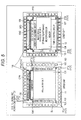
- Fig. 6 is a diagram illustrating an exemplary layout of the power supply wiring in the floorplans of the first chip and the second chip according to the embodiment.
- the power wiring LPWR is supplied from PAD-A and PAD-B of the second chip (lower chip) 12 illustrated in Fig. 6 .
- PAD-A and PAD-B are connected to TCVs near the circuit block on the first chip (upper chip) 11 to which power is to be supplied with a sufficiently low impedance.
- the power supply wiring LPWR for power supplied through the TCVs is directly connected to the ports PTU of the circuit blocks.
- the signal wiring LCS for control signals output from the timing control circuit 107 of the second chip (lower chip) 12 is connected to TCVs near shorter edges of the circuit block on the first chip (upper chip) 11 to which the wiring is to be connected.
- the signals are input to the ports PTU of the circuit block on the first chip (upper chip) 11 via the TCVs.
- the circuit block on the first chip (upper chip) 11 includes the vertical drive circuit 102 and the vertical decoder 103 in the example of Fig. 6 .
- Fig. 7 is an enlarged view of a part circled by a circle A in Fig. 6 and illustrates a specific example of TCVs arranged near a circuit block (the vertical decoder in this example).
- Fig. 8 is a diagram illustrating a cross-section structure taken along line A-A' in Fig. 7 . In Fig. 7 , only components related to wiring on the first chip (upper chip) 11 are illustrated.
- TCV 1 to TCV 5 are TCVs for power supply and connect the power supply wiring LPWR for power supplied from the second chip (lower chip) 12 to the circuit block CBLK on the first chip (upper chip) 11.
- TCV 7 to TCV 9 are TCVs for supplying control signals and connect the signal wiring LCS for control signals between the upper and lower chips.
- On the first chip (upper chip) 11 spaces between TCVs for power supply are used for wiring of a wiring layer (not illustrated) different from the wiring layer for TCV connections and connected to the circuit block CBLK.
- the signal wiring LCS is provided in gaps between columns of TCVs 121 and 122 avoiding the columns.
- TCV 1 to TCV 5 for power supply are arranged inside of TCV 7 to TCV 9 for supplying control signals with respect to the edge of the chip.
- the wirings are formed of Al and Cu.
- a case where the uppermost layer of the first chip (upper chip) 11 and the uppermost layer of the second chip (lower chip) 12 are connected by TCV connections CNT is illustrated as an example.
- Fig. 8 merely illustrates one example of TCV connections, and the use of wiring layers and the positions of circuits on each of the upper and lower chips are arbitrary and thus not limited thereto.
- the impedance of the power supply wiring LPWR in the circuit block on the first chip (upper chip) 11 may be increased, which may lead to malfunction of the circuit block. If the power supply wiring is simply made thicker, the chip size will be increased. Thus, it is also possible to enhance the power supply of the power supply wiring LPWR on the first chip (upper chip) 11 using the wirings of the second chip (lower chip) 12 as measures against noise and for stable supply.
- Fig. 9 is a diagram illustrating a modified example of the circuit block wiring of Fig. 8 .
- Fig. 10 is a diagram illustrating a cross-section structure taken along line B-B' in Fig. 9 .
- wiring necessary for connections in logic circuits on the second chip (lower chip) 12 is not illustrated for simplification.
- the circuit block is divided into two circuit blocks CBLK1 and CBLK2, and TCVs are arranged in spaces therein. Then, the second chip (lower chip) 12 is backed with power supply line LPWRB provided in parallel with power supply wiring LPWRU on the first chip (upper chip) 11.
- connection between the upper and lower chips is achieved through TCVs, and since the arrangement pitch is sufficiently small owing to the structure thereof and the TCVs are processed during wafer processes, the yield is less likely to be lowered. Moreover, since DC components of power supply and reference signals from the second chip (lower chip) 12 to the first chip (upper chip) 11 are supplied via the TCVs, special circuits for communication are not necessary, and the cost can be reduced as a result.
- the following effects can be produced according to the embodiment.
- the problem of noise at TCV connections can be reduced and a circuit configuration most suitable for the circuit layout between the upper and lower chips can be achieved.
- the upper chip can achieve characteristics excellent in resistance to noise.
- the lower chip can use a general ASIC (Logic) process.
- the vertical decoder 103 that is a digital circuit is arranged on the first chip 11 in the configuration of Fig. 4 in the embodiment. It is also possible, however, to employ other configurations.
- Fig. 11 is a block diagram illustrating a second exemplary configuration of the solid-state image sensor according to the embodiment.
- the solid-state image sensor 10B may be configured such that the vertical decoder 103 is mounted on a second chip 12B, and analog circuits and digital circuits are mounted on different chips as illustrated in Fig. 11 .
- Fig. 12 is a block diagram illustrating a third exemplary configuration of the solid-state image sensor according to the embodiment.
- Fig. 13 is a diagram illustrating an example of floorplans of the first chip and the second chip in the solid-state image sensor of Fig. 12 .
- the solid-state image sensor can also be configured as illustrated in Fig. 12 so as to reduce the chip size thereof.
- part of the vertical drive circuit (row scanning circuit) 102 and the vertical decoder 103 among the circuits to be mounted on the first chip (upper chip) 11 can be moved onto the second chip (lower chip) 12.
- the vertical drive circuit (row scanning circuit) 102 and the vertical decoder 103 may be separately mounted on the first chip (upper chip) 11 and the second chip (lower chip) 12, respectively.
- the vertical drive circuit (row scanning circuit) 102 and the vertical decoder 103 may be integrated into one functional block and part thereof may be mounted on the first chip (upper chip) 11 and the rest thereof may be mounted on the second chip (lower chip) 12.
- Fig. 14 is a block diagram illustrating a fourth exemplary configuration of the solid-state image sensor according to the embodiment.
- Fig. 15 is a diagram illustrating an example of floorplans of the first chip and the second chip in the solid-state image sensor of Fig. 14 .
- the solid-state image sensor may be configured as illustrated in Fig. 14 .
- the whole of the vertical drive circuit (row scanning circuit) 102 and the vertical decoder 103, and the reference signal supply unit 105 can be mounted on the second chip (lower chip) 12.
- the noise amount of the second chip (lower chip) 12 should be paid attention to. Because the reference signal supply unit 105 is less likely to be affected by noise as compared to the comparator 1041, however, the reference signal supply unit 105 can be mounted on the second chip (lower chip) 12.
- the circuit size of the image signal processing unit is smaller, but the vertical drive circuit (row scanning circuit) 102, the vertical decoder 103 and the reference signal supply unit 105 are mounted on the second chip (lower chip) 12.
- the first chip (upper chip) 11 does not include the whole of the vertical drive circuit (row scanning circuit) 102 and the vertical decoder 103, and the reference signal supply unit 105, and the chip size thereof is reduced.
- part of the vertical drive circuit (row scanning circuit) 102 and the vertical decoder 103 may be mounted on the first chip (upper chip) 11.
- PADs are arranged in two rows on two sides on the left and on the right in the example of Fig. 15 , various arrangements such as arrangement on four sides, arrangement on three sides and arrangement in two rows on two sides are possible for PAD arrangement where reservation of PAD areas and mounting on a lens module are considered.
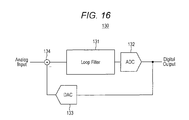
- Fig. 16 is a block diagram illustrating a basic configuration of the ⁇ ADC (AD) converter.
- the ⁇ ADC 130 includes a filter part 131, an A-D converter (ADC) 132 with a low resolution of 1 to 5 bits, a D-A converter (DAC) 133 with the same number of bits as the ADC, and a subtractor 134 in an input stage. Since the ⁇ ADC 130 is a system using feedback, the nonlinearity of the circuit and the noise are reduced and a high resolution can be achieved.
- ADC A-D converter
- DAC D-A converter
- the ⁇ ADC 130 Since it is more difficult for the ⁇ ADC 130 to reduce the nonlinearity of the circuit and the noise for a part nearer to an analog input, it is desired that an input circuit of the filter part 131 and the DAC 133 have high linearity and low noise.
- the nonlinearity of the DAC 133 causes an increase in the noise floor, and it is thus important to ensure the linearity of the DAC when an ADC with bits other than one bit is used.
- Fig. 17 is a diagram illustrating a basic configuration of a pixel array peripheral part when the ⁇ ADC is employed in the column processing unit of the solid-state image sensor.
- the column processing unit 140 in Fig. 17 includes a column circuit 141 that performs processes such as CDS and a ⁇ modulator ( ⁇ ADC) 142 that performs an ADC process.
- ⁇ ADC ⁇ modulator
- an oversampling method mainly targeting at reduction of noise is employed.
- Figs. 18(A) to 18(C) are diagrams for explaining the oversampling methods.
- a first method is oversampling by performing readout at high speed during a video frame rate as illustrated in Fig. 18(A) .
- a second method is oversampling within a frame by non-destructive readout as illustrated in Fig. 18(B) .
- a third method is oversampling on a constant sampled value as illustrated in Fig. 18(C) .
- the third method for example, is employed for the column processing unit 140 of Fig. 17 .
- a ⁇ modulation output (ADC output) resulting from the oversampling is converted into a normal frame rate of N bits by a digital filter.
- Fig. 19 is a diagram illustrating a first exemplary configuration of the pixel array peripheral part when a digital filter is employed for the column processing unit including a ⁇ ADC.
- Fig. 20 is a diagram illustrating a second exemplary configuration of the pixel array peripheral part when a digital filter is employed for the column processing unit including a ⁇ ADC.
- the column processing unit 140A in Fig. 19 has a digital filter 143 arranged at the output of the ⁇ modulator 142 and an output control circuit 144 arranged at the output of the digital filter 143.
- the column processing unit 140B in Fig. 20 has the output control circuit 144 arranged at the output of the ⁇ modulator 142 and the digital filter 143 arranged at the output of the output control circuit 144.
- the digital filter 143 can be a programmable filter by being implemented by software.
- Fig. 21 is a block diagram illustrating a fifth exemplary configuration of the solid-state image sensor according to the embodiment.
- the solid-state image sensor 10E in Fig. 21 has an exemplary configuration in a case where the column processing units 140A and 140B in Figs. 19 and 20 are employed.
- an edge part where video data signals are communicated between the first chip 11 and the second chip 12 is an output part of the ⁇ modulator that is a boundary circuit among analog circuits with digital circuits.
- the column circuit 141 and the ⁇ modulator ( ⁇ ADC) 142 that performs an ADC process are arranged on the first chip 11E.
- the digital filter 143 and the output control circuit 144 are arranged on the second chip 12E.
- Fig. 21 can similarly be employed in configurations similar to those of Figs. 11 , 12 and 14 .
- CMOS image sensor While the configuration of the CMOS image sensor is described as an example of the semiconductor device in this embodiment, the configuration can also be applied to a back side illuminated CMOS image sensor, for example, and the effects described above can also be produced in this case.
- a front side illuminated image sensor can also sufficiently produce the effects described above.
- a solid-state image sensor having such a configuration can be applied as an imaging device for a digital camera and a video camera.
- Fig. 22 is a diagram illustrating an example of a configuration of a camera system to which a solid-state image sensor according to an embodiment of the present invention is applied.
- the camera system 200 includes an imaging device 210 to which the CMOS image sensors (solid-state image sensors) 10, 10A to 10E according to the embodiment can be applied.
- the camera system 200 further includes an optical system that guides input light to (form a subject image on) a pixel area of the imaging device 210, such as a lens 220 that focuses input light (image light) on an imaging plane.
- the camera system 200 includes a drive circuit (DRV) 230 that drives the imaging device 210, and a signal processing circuit (PRC) 240 that processes signals output from the imaging device 210.
- DUV drive circuit
- PRC signal processing circuit
- the drive circuit 230 has a timing generator (not illustrated) that generates various timing signals including a start pulse and a clock pulse for driving circuits in the imaging device 210, and drives the imaging device 210 with predetermined timing signals.
- the signal processing circuit 240 performs predetermined signal processing on signals output from the imaging device 210.
- Image signals processed by the signal processing circuit 240 are recorded on a recording medium such as a memory.
- the image information recorded on the recording medium is output in hard copy by a printer or the like.
- the image signals processed by the signal processing circuit 240 are displayed as moving images on a monitor such as a liquid crystal display.
- a high-resolution camera can be realized by mounting the image sensors 10, 10A to 10E described above as the imaging device 210 in an image pick up apparatus such as a digital still camera.
- 10, 10A to 10E solid-state image sensor (semiconductor device), 11 ... first chip (upper chip), 12 ... second chip (lower chip), 101 ... pixel array unit, 102 ... vertical drive circuit (row scanning circuit), 103 ... vertical decoder, 104 ... column processing unit, 1041 ... comparator, 1042 ... counter circuit, 105 ... reference signal supply unit, 106 ... horizontal scanning circuit (column scanning circuit), 107 ... timing control circuit, 108 ... image signal processing unit, 109 ... I/F circuits, LPWR ... power supply wiring, LCS ... signal wiring, 120, 121, 122, 1 to 9 ... TCV, 130 ... ⁇ modulator ( ⁇ ADC), 140 ... column processing unit, 141 ... column circuit, 142 ... ⁇ modulator ( ⁇ ADC), 143 ... digital filter, 144 ... output control circuit, CBLK, CBLK1, CBLK2 ... circuit block, 200 ... camera system
Landscapes
- Engineering & Computer Science (AREA)
- Multimedia (AREA)
- Signal Processing (AREA)
- Solid State Image Pick-Up Elements (AREA)
- Transforming Light Signals Into Electric Signals (AREA)
- Semiconductor Integrated Circuits (AREA)
Priority Applications (3)
| Application Number | Priority Date | Filing Date | Title |
|---|---|---|---|
| EP19167097.5A EP3525237A1 (de) | 2010-01-08 | 2010-12-28 | Halbleiterbauelement, festkörperbildsensor und kamerasystem |
| EP17183032.6A EP3267480B1 (de) | 2010-01-08 | 2010-12-28 | Festkörperbildsensor und kamerasystem |
| EP19159427.4A EP3528284A3 (de) | 2010-01-08 | 2010-12-28 | Halbleiterbauelement, festkörperbildsensor und kamerasystem |
Applications Claiming Priority (3)
| Application Number | Priority Date | Filing Date | Title |
|---|---|---|---|
| JP2010002979 | 2010-01-08 | ||
| JP2010255934A JP5685898B2 (ja) | 2010-01-08 | 2010-11-16 | 半導体装置、固体撮像装置、およびカメラシステム |
| PCT/JP2010/073671 WO2011083722A1 (ja) | 2010-01-08 | 2010-12-28 | 半導体装置、固体撮像装置、およびカメラシステム |
Related Child Applications (6)
| Application Number | Title | Priority Date | Filing Date |
|---|---|---|---|
| EP19159427.4A Division-Into EP3528284A3 (de) | 2010-01-08 | 2010-12-28 | Halbleiterbauelement, festkörperbildsensor und kamerasystem |
| EP19159427.4A Division EP3528284A3 (de) | 2010-01-08 | 2010-12-28 | Halbleiterbauelement, festkörperbildsensor und kamerasystem |
| EP17183032.6A Division-Into EP3267480B1 (de) | 2010-01-08 | 2010-12-28 | Festkörperbildsensor und kamerasystem |
| EP17183032.6A Division EP3267480B1 (de) | 2010-01-08 | 2010-12-28 | Festkörperbildsensor und kamerasystem |
| EP19167097.5A Division-Into EP3525237A1 (de) | 2010-01-08 | 2010-12-28 | Halbleiterbauelement, festkörperbildsensor und kamerasystem |
| EP19167097.5A Division EP3525237A1 (de) | 2010-01-08 | 2010-12-28 | Halbleiterbauelement, festkörperbildsensor und kamerasystem |
Publications (3)
| Publication Number | Publication Date |
|---|---|
| EP2528093A1 true EP2528093A1 (de) | 2012-11-28 |
| EP2528093A4 EP2528093A4 (de) | 2014-03-26 |
| EP2528093B1 EP2528093B1 (de) | 2019-05-15 |
Family
ID=44306407
Family Applications (4)
| Application Number | Title | Priority Date | Filing Date |
|---|---|---|---|
| EP17183032.6A Active EP3267480B1 (de) | 2010-01-08 | 2010-12-28 | Festkörperbildsensor und kamerasystem |
| EP10842233.8A Active EP2528093B1 (de) | 2010-01-08 | 2010-12-28 | Festkörperabbildungsvorrichtung und kamerasystem |
| EP19167097.5A Pending EP3525237A1 (de) | 2010-01-08 | 2010-12-28 | Halbleiterbauelement, festkörperbildsensor und kamerasystem |
| EP19159427.4A Withdrawn EP3528284A3 (de) | 2010-01-08 | 2010-12-28 | Halbleiterbauelement, festkörperbildsensor und kamerasystem |
Family Applications Before (1)
| Application Number | Title | Priority Date | Filing Date |
|---|---|---|---|
| EP17183032.6A Active EP3267480B1 (de) | 2010-01-08 | 2010-12-28 | Festkörperbildsensor und kamerasystem |
Family Applications After (2)
| Application Number | Title | Priority Date | Filing Date |
|---|---|---|---|
| EP19167097.5A Pending EP3525237A1 (de) | 2010-01-08 | 2010-12-28 | Halbleiterbauelement, festkörperbildsensor und kamerasystem |
| EP19159427.4A Withdrawn EP3528284A3 (de) | 2010-01-08 | 2010-12-28 | Halbleiterbauelement, festkörperbildsensor und kamerasystem |
Country Status (8)
| Country | Link |
|---|---|
| US (9) | US9093363B2 (de) |
| EP (4) | EP3267480B1 (de) |
| JP (1) | JP5685898B2 (de) |
| KR (3) | KR101774609B1 (de) |
| CN (1) | CN102782840B (de) |
| DE (2) | DE202010018564U1 (de) |
| TW (1) | TWI456731B (de) |
| WO (1) | WO2011083722A1 (de) |
Cited By (8)
| Publication number | Priority date | Publication date | Assignee | Title |
|---|---|---|---|---|
| EP2889908A1 (de) * | 2013-12-26 | 2015-07-01 | Sony Corporation | Elektronische Vorrichtung |
| US9748291B2 (en) | 2014-09-26 | 2017-08-29 | Semiconductor Energy Laboratory Co., Ltd. | Imaging device having a third circuit with a region overlapping with a fourth circuit |
| EP3570325A4 (de) * | 2017-01-12 | 2019-12-04 | Mitsubishi Electric Corporation | Infrarotsensorsubstrat und infrarotsensorvorrichtung |
| US10735651B2 (en) | 2012-07-06 | 2020-08-04 | Sony Corporation | Solid-state imaging device and driving method of solid-state imaging device, and electronic equipment |
| EP3706169A4 (de) * | 2017-10-30 | 2020-12-16 | Sony Semiconductor Solutions Corporation | Festkörperabbildungsvorrichtung mit rückseitenbestrahlung, verfahren zur herstellung einer festkörperabbildungsvorrichtung mit rückseitenbestrahlung, abbildungsvorrichtung und elektronische vorrichtung |
| EP3713222A4 (de) * | 2019-01-31 | 2020-12-23 | Shenzhen Goodix Technology Co., Ltd. | Bildsensor und herstellungsverfahren dafür sowie elektronische vorrichtung |
| US11557624B2 (en) | 2016-03-24 | 2023-01-17 | Nikon Corporation | Image sensor and image capturing device |
| US12120449B2 (en) | 2019-01-25 | 2024-10-15 | Sony Semiconductor Solutions Corporation | Image capturing device and electronic apparatus with stacked chip structure |
Families Citing this family (111)
| Publication number | Priority date | Publication date | Assignee | Title |
|---|---|---|---|---|
| WO2010073520A1 (ja) * | 2008-12-26 | 2010-07-01 | パナソニック株式会社 | 固体撮像デバイスおよびその製造方法 |
| JP5685898B2 (ja) | 2010-01-08 | 2015-03-18 | ソニー株式会社 | 半導体装置、固体撮像装置、およびカメラシステム |
| JP6173410B2 (ja) * | 2010-06-30 | 2017-08-02 | キヤノン株式会社 | 固体撮像装置および固体撮像装置の製造方法 |
| JP5843475B2 (ja) * | 2010-06-30 | 2016-01-13 | キヤノン株式会社 | 固体撮像装置および固体撮像装置の製造方法 |
| JP5791571B2 (ja) | 2011-08-02 | 2015-10-07 | キヤノン株式会社 | 撮像素子及び撮像装置 |
| JP6091550B2 (ja) * | 2011-08-02 | 2017-03-08 | キヤノン株式会社 | 撮像素子及び撮像装置 |
| US8890047B2 (en) * | 2011-09-21 | 2014-11-18 | Aptina Imaging Corporation | Stacked-chip imaging systems |
| JP5645786B2 (ja) * | 2011-09-22 | 2014-12-24 | 富士フイルム株式会社 | 固体撮像装置及びカメラモジュール |
| JP2013090305A (ja) | 2011-10-21 | 2013-05-13 | Sony Corp | 比較器、ad変換器、固体撮像装置、およびカメラシステム |
| JP6056126B2 (ja) | 2011-10-21 | 2017-01-11 | ソニー株式会社 | 固体撮像装置およびカメラシステム |
| JP5923929B2 (ja) | 2011-10-27 | 2016-05-25 | ソニー株式会社 | 固体撮像素子およびカメラシステム |
| JP2014241458A (ja) * | 2011-10-28 | 2014-12-25 | ソニー株式会社 | 固体撮像素子およびカメラシステム |
| JP6016378B2 (ja) | 2012-02-29 | 2016-10-26 | キヤノン株式会社 | 光電変換装置、および光電変換装置を用いた撮像システム |
| JP6214132B2 (ja) | 2012-02-29 | 2017-10-18 | キヤノン株式会社 | 光電変換装置、撮像システムおよび光電変換装置の製造方法 |
| US9607971B2 (en) | 2012-06-04 | 2017-03-28 | Sony Corporation | Semiconductor device and sensing system |
| US8710607B2 (en) * | 2012-07-12 | 2014-04-29 | Taiwan Semiconductor Manufacturing Company, Ltd. | Method and apparatus for image sensor packaging |
| US9343497B2 (en) * | 2012-09-20 | 2016-05-17 | Semiconductor Components Industries, Llc | Imagers with stacked integrated circuit dies |
| JP6128787B2 (ja) | 2012-09-28 | 2017-05-17 | キヤノン株式会社 | 半導体装置 |
| US9389315B2 (en) | 2012-12-19 | 2016-07-12 | Basf Se | Detector comprising a transversal optical sensor for detecting a transversal position of a light beam from an object and a longitudinal optical sensor sensing a beam cross-section of the light beam in a sensor region |
| JP6037878B2 (ja) * | 2013-02-13 | 2016-12-07 | オリンパス株式会社 | 撮像装置 |
| US8946784B2 (en) * | 2013-02-18 | 2015-02-03 | Taiwan Semiconductor Manufacturing Company, Ltd. | Method and apparatus for image sensor packaging |
| JP2014165396A (ja) * | 2013-02-26 | 2014-09-08 | Sony Corp | 固体撮像装置および電子機器 |
| WO2014141663A1 (ja) * | 2013-03-14 | 2014-09-18 | 株式会社ニコン | 撮像ユニット、撮像装置および撮像制御プログラム |
| AU2014280332B2 (en) | 2013-06-13 | 2017-09-07 | Basf Se | Detector for optically detecting at least one object |
| US10353049B2 (en) | 2013-06-13 | 2019-07-16 | Basf Se | Detector for optically detecting an orientation of at least one object |
| CN105210190A (zh) * | 2013-06-13 | 2015-12-30 | 巴斯夫欧洲公司 | 光学检测器及其制造方法 |
| JP6190184B2 (ja) * | 2013-06-28 | 2017-08-30 | キヤノン株式会社 | 撮像素子、撮像装置、その制御方法、および制御プログラム |
| TWI631854B (zh) * | 2013-08-05 | 2018-08-01 | 日商新力股份有限公司 | Conversion device, imaging device, electronic device, conversion method |
| TWI659652B (zh) | 2013-08-05 | 2019-05-11 | 新力股份有限公司 | 攝像裝置、電子機器 |
| AU2014310703B2 (en) | 2013-08-19 | 2018-09-27 | Basf Se | Optical detector |
| JP6192469B2 (ja) | 2013-10-01 | 2017-09-06 | オリンパス株式会社 | 撮像装置 |
| JP6346740B2 (ja) * | 2013-10-08 | 2018-06-20 | オリンパス株式会社 | 撮像装置 |
| JP6463944B2 (ja) | 2013-11-25 | 2019-02-06 | キヤノン株式会社 | 撮像素子、撮像装置及び携帯電話機 |
| JP6458114B2 (ja) * | 2013-11-29 | 2019-01-23 | キヤノン株式会社 | 撮像素子、撮像装置及び携帯電話機 |
| JP6320272B2 (ja) * | 2013-11-29 | 2018-05-09 | キヤノン株式会社 | 撮像素子、撮像装置及び携帯電話機 |
| JP6278881B2 (ja) * | 2013-12-06 | 2018-02-14 | キヤノン株式会社 | 撮像素子、撮像装置及び携帯電話機 |
| US9536920B2 (en) * | 2014-03-28 | 2017-01-03 | Taiwan Semiconductor Manufacturing Company, Ltd. | Stacked image sensor having a barrier layer |
| JP2015195235A (ja) * | 2014-03-31 | 2015-11-05 | ソニー株式会社 | 固体撮像素子、電子機器、および撮像方法 |
| US20150296158A1 (en) * | 2014-04-10 | 2015-10-15 | Forza Silicon Corporation | Reconfigurable CMOS Image Sensor |
| TWI648986B (zh) | 2014-04-15 | 2019-01-21 | Sony Corporation | 攝像元件、電子機器 |
| US9794499B2 (en) * | 2014-04-29 | 2017-10-17 | Fermi Research Alliance, Llc | Wafer-scale pixelated detector system |
| US10084983B2 (en) | 2014-04-29 | 2018-09-25 | Fermi Research Alliance, Llc | Wafer-scale pixelated detector system |
| CN104092963B (zh) * | 2014-06-24 | 2018-01-02 | 上海集成电路研发中心有限公司 | 一种可重构的cmos图像传感器芯片及其形成方法 |
| WO2016005893A1 (en) | 2014-07-08 | 2016-01-14 | Basf Se | Detector for determining a position of at least one object |
| US9531959B2 (en) * | 2014-08-29 | 2016-12-27 | Semiconductor Components Industries, Llc | Imaging systems and methods for capturing image data at high scan rates |
| KR102452393B1 (ko) | 2014-09-29 | 2022-10-11 | 바스프 에스이 | 적어도 하나의 물체의 포지션을 광학적으로 결정하기 위한 방법 및 검출기 및 이를 이용한 휴먼 머신 인터페이스, 엔터테인먼트 장치, 추적 시스템, 스캐닝 시스템, 입체 시스템 및 카메라 |
| JP6930556B2 (ja) * | 2014-09-30 | 2021-09-01 | 株式会社ニコン | 撮像素子および撮像装置 |
| US11125880B2 (en) | 2014-12-09 | 2021-09-21 | Basf Se | Optical detector |
| US10070088B2 (en) * | 2015-01-05 | 2018-09-04 | Canon Kabushiki Kaisha | Image sensor and image capturing apparatus for simultaneously performing focus detection and image generation |
| JP6218799B2 (ja) | 2015-01-05 | 2017-10-25 | キヤノン株式会社 | 撮像素子及び撮像装置 |
| EP3251152B1 (de) | 2015-01-30 | 2023-08-16 | Trinamix GmbH | Detektor für die optische erfassung eines objektes |
| US10389961B2 (en) | 2015-04-09 | 2019-08-20 | Semiconductor Energy Laboratory Co., Ltd. | Imaging device and electronic device |
| CN107534049B (zh) | 2015-04-24 | 2021-07-20 | 索尼公司 | 固态图像元件、半导体装置和电子设备 |
| TWI692859B (zh) * | 2015-05-15 | 2020-05-01 | 日商新力股份有限公司 | 固體攝像裝置及其製造方法、以及電子機器 |
| JP6272387B2 (ja) * | 2015-05-29 | 2018-01-31 | キヤノン株式会社 | 撮像素子および撮像装置 |
| JP6608185B2 (ja) * | 2015-06-18 | 2019-11-20 | キヤノン株式会社 | 積層型イメージセンサおよび撮像装置 |
| WO2017012986A1 (en) | 2015-07-17 | 2017-01-26 | Trinamix Gmbh | Detector for optically detecting at least one object |
| KR102422224B1 (ko) | 2015-07-31 | 2022-07-18 | 삼성전자주식회사 | 적층형 이미지 센서 및 이를 포함하는 시스템 |
| KR102653044B1 (ko) | 2015-09-01 | 2024-04-01 | 소니그룹주식회사 | 적층체 |
| JP6755316B2 (ja) | 2015-09-14 | 2020-09-16 | トリナミクス ゲゼルシャフト ミット ベシュレンクテル ハフツング | 少なくとも1つの物体の少なくとも1つの画像を記録するカメラ |
| US11297258B2 (en) * | 2015-10-01 | 2022-04-05 | Qualcomm Incorporated | High dynamic range solid state image sensor and camera system |
| JPWO2017077620A1 (ja) * | 2015-11-05 | 2018-09-20 | オリンパス株式会社 | 固体撮像装置 |
| TWI648586B (zh) * | 2016-03-15 | 2019-01-21 | 寧波舜宇光電信息有限公司 | Camera module and array camera module based on integrated packaging process |
| US10998373B2 (en) | 2016-07-11 | 2021-05-04 | Sony Semiconductor Solutions Corporation | Imaging element and imaging device |
| KR102492134B1 (ko) | 2016-07-29 | 2023-01-27 | 트리나미엑스 게엠베하 | 광학 센서 및 광학적 검출용 검출기 |
| JP2018042139A (ja) * | 2016-09-08 | 2018-03-15 | ソニーセミコンダクタソリューションズ株式会社 | 撮像素子および撮像素子の動作方法、撮像装置、および電子機器 |
| JP2019532517A (ja) | 2016-10-25 | 2019-11-07 | トリナミクス ゲゼルシャフト ミット ベシュレンクテル ハフツング | 光学的に検出するための光検出器 |
| US11428787B2 (en) | 2016-10-25 | 2022-08-30 | Trinamix Gmbh | Detector for an optical detection of at least one object |
| US11860292B2 (en) | 2016-11-17 | 2024-01-02 | Trinamix Gmbh | Detector and methods for authenticating at least one object |
| EP3542179B1 (de) | 2016-11-17 | 2021-03-24 | trinamiX GmbH | Detektor zur optischen detektion von mindestens einem objekt |
| JP7204667B2 (ja) | 2017-04-20 | 2023-01-16 | トリナミクス ゲゼルシャフト ミット ベシュレンクテル ハフツング | 光検出器 |
| JP7237024B2 (ja) | 2017-06-26 | 2023-03-10 | トリナミクス ゲゼルシャフト ミット ベシュレンクテル ハフツング | 少なくとも1つの物体の位置を決定するための検出器 |
| WO2019004276A1 (en) * | 2017-06-29 | 2019-01-03 | Sony Semiconductor Solutions Corporation | BACKLIT IMAGEER LINKED TO A SLICER |
| JP7102119B2 (ja) | 2017-09-29 | 2022-07-19 | キヤノン株式会社 | 半導体装置および機器 |
| US10529757B2 (en) | 2017-12-15 | 2020-01-07 | Atomera Incorporated | CMOS image sensor including pixels with read circuitry having a superlattice |
| US10608043B2 (en) * | 2017-12-15 | 2020-03-31 | Atomera Incorporation | Method for making CMOS image sensor including stacked semiconductor chips and readout circuitry including a superlattice |
| US10367028B2 (en) | 2017-12-15 | 2019-07-30 | Atomera Incorporated | CMOS image sensor including stacked semiconductor chips and image processing circuitry including a superlattice |
| US10529768B2 (en) | 2017-12-15 | 2020-01-07 | Atomera Incorporated | Method for making CMOS image sensor including pixels with read circuitry having a superlattice |
| US10615209B2 (en) | 2017-12-15 | 2020-04-07 | Atomera Incorporated | CMOS image sensor including stacked semiconductor chips and readout circuitry including a superlattice |
| US10608027B2 (en) * | 2017-12-15 | 2020-03-31 | Atomera Incorporated | Method for making CMOS image sensor including stacked semiconductor chips and image processing circuitry including a superlattice |
| US10708529B2 (en) * | 2017-12-20 | 2020-07-07 | Semiconductor Components Industries, Llc | Image sensors with low-voltage transistors |
| CN108281412B (zh) * | 2018-01-23 | 2020-02-14 | 德淮半导体有限公司 | 堆叠式图像传感器、像素管芯及其制造方法 |
| JP7527755B2 (ja) * | 2018-02-09 | 2024-08-05 | キヤノン株式会社 | 光電変換装置および撮像システム |
| JP7080660B2 (ja) * | 2018-02-09 | 2022-06-06 | キヤノン株式会社 | 光電変換装置、撮像システム、および、移動体 |
| JP6575635B2 (ja) * | 2018-04-26 | 2019-09-18 | ソニー株式会社 | 半導体装置、固体撮像装置、およびカメラシステム |
| US10530380B2 (en) * | 2018-04-27 | 2020-01-07 | Raytheon Company | Massively parallel three dimensional per pixel single slope analog to digital converter |
| JP6669196B2 (ja) * | 2018-05-28 | 2020-03-18 | 株式会社ニコン | 撮像素子及び撮像装置 |
| JP6708698B2 (ja) * | 2018-05-31 | 2020-06-10 | キヤノン株式会社 | 光電変換装置、および光電変換装置を用いた撮像システム |
| WO2020027230A1 (ja) | 2018-07-31 | 2020-02-06 | ソニーセミコンダクタソリューションズ株式会社 | 積層型受光センサ及び車載撮像装置 |
| WO2020027233A1 (ja) * | 2018-07-31 | 2020-02-06 | ソニーセミコンダクタソリューションズ株式会社 | 撮像装置及び車両制御システム |
| KR102899656B1 (ko) * | 2018-07-31 | 2025-12-11 | 소니 세미컨덕터 솔루션즈 가부시키가이샤 | 적층형 수광 센서 및 전자기기 |
| JP7327916B2 (ja) * | 2018-09-11 | 2023-08-16 | キヤノン株式会社 | 光電変換装置および機器 |
| JP7402606B2 (ja) * | 2018-10-31 | 2023-12-21 | ソニーセミコンダクタソリューションズ株式会社 | 固体撮像装置及び電子機器 |
| US12119359B2 (en) * | 2018-12-20 | 2024-10-15 | Sony Semiconductor Solutions Corporation | Imaging device |
| TWI692857B (zh) * | 2019-01-25 | 2020-05-01 | 世界先進積體電路股份有限公司 | 半導體裝置與生物辨識裝置 |
| KR102756185B1 (ko) | 2019-03-15 | 2025-01-17 | 삼성전자주식회사 | 디스플레이 드라이버 ic 소자 |
| US12058459B2 (en) | 2019-05-10 | 2024-08-06 | Sony Advanced Visual Sensing Ag | NMOS comparator for image sensor pixel |
| JP6957559B2 (ja) | 2019-06-24 | 2021-11-02 | キヤノン株式会社 | 半導体装置および機器 |
| JP7279746B2 (ja) * | 2019-06-27 | 2023-05-23 | 株式会社ニコン | 撮像ユニットおよび撮像装置 |
| JP7599938B2 (ja) * | 2020-01-10 | 2024-12-16 | キヤノン株式会社 | 撮像素子ユニット及び撮像装置 |
| JP2020096367A (ja) * | 2020-02-27 | 2020-06-18 | 株式会社ニコン | 画像処理装置および撮像装置 |
| JP7171649B2 (ja) * | 2020-05-15 | 2022-11-15 | キヤノン株式会社 | 撮像装置および撮像システム |
| ES2962472T3 (es) * | 2020-06-26 | 2024-03-19 | Alpsentek Gmbh | Sensor de imagen delta con almacenamiento de píxeles digital |
| JP7690308B2 (ja) * | 2021-03-31 | 2025-06-10 | キヤノン株式会社 | 光電変換装置、光電変換システム、および移動体 |
| JP7551558B2 (ja) | 2021-04-01 | 2024-09-17 | キヤノン株式会社 | 信号処理装置 |
| CN115241215B (zh) * | 2021-04-22 | 2025-10-31 | 联合微电子中心有限责任公司 | 图像传感器和半导体封装 |
| JP7851092B2 (ja) | 2021-10-01 | 2026-04-24 | キヤノン株式会社 | 撮像装置及び電子機器 |
| JP7759804B2 (ja) * | 2021-12-28 | 2025-10-24 | シャープセミコンダクターイノベーション株式会社 | 固体撮像素子及び電子装置 |
| CN116417403A (zh) * | 2021-12-30 | 2023-07-11 | 联华电子股份有限公司 | 半导体元件及其制作方法 |
| US20230299109A1 (en) * | 2022-03-18 | 2023-09-21 | Taiwan Semiconductor Manufacturing Company, Ltd. | Stacked image sensors and methods of manufacturing thereof |
| JP2023142256A (ja) * | 2022-03-24 | 2023-10-05 | ソニーセミコンダクタソリューションズ株式会社 | 固体撮像装置及び半導体装置の製造方法 |
Family Cites Families (65)
| Publication number | Priority date | Publication date | Assignee | Title |
|---|---|---|---|---|
| JP3432963B2 (ja) * | 1995-06-15 | 2003-08-04 | 沖電気工業株式会社 | 半導体集積回路 |
| US6271785B1 (en) * | 1998-04-29 | 2001-08-07 | Texas Instruments Incorporated | CMOS imager with an A/D per pixel convertor |
| US7129985B1 (en) * | 1998-11-24 | 2006-10-31 | Canon Kabushiki Kaisha | Image sensing apparatus arranged on a single substrate |
| AU2003900746A0 (en) * | 2003-02-17 | 2003-03-06 | Silverbrook Research Pty Ltd | Methods, systems and apparatus (NPS041) |
| JP3737333B2 (ja) * | 2000-03-17 | 2006-01-18 | 沖電気工業株式会社 | 半導体装置 |
| JP2001289886A (ja) * | 2000-04-03 | 2001-10-19 | Sanyo Electric Co Ltd | 電池電圧測定装置 |
| JP3713418B2 (ja) * | 2000-05-30 | 2005-11-09 | 光正 小柳 | 3次元画像処理装置の製造方法 |
| US6809769B1 (en) * | 2000-06-22 | 2004-10-26 | Pixim, Inc. | Designs of digital pixel sensors |
| US7139024B2 (en) * | 2002-07-26 | 2006-11-21 | Xerox Corporation | Large-area imager with direct digital pixel output |
| JP3652676B2 (ja) * | 2002-09-17 | 2005-05-25 | 松下電器産業株式会社 | 撮像装置および画像ピックアップシステム |
| JP2004146816A (ja) | 2002-09-30 | 2004-05-20 | Matsushita Electric Ind Co Ltd | 固体撮像装置およびこれを用いた機器 |
| CN1234234C (zh) * | 2002-09-30 | 2005-12-28 | 松下电器产业株式会社 | 固体摄像器件及使用该固体摄像器件的设备 |
| JP4414646B2 (ja) * | 2002-11-18 | 2010-02-10 | 浜松ホトニクス株式会社 | 光検出装置 |
| KR100494474B1 (ko) * | 2003-01-14 | 2005-06-10 | 삼성전기주식회사 | 카메라 모듈 및 그 제조방법 |
| KR100568223B1 (ko) * | 2003-06-18 | 2006-04-07 | 삼성전자주식회사 | 고체 촬상용 반도체 장치 |
| US6927432B2 (en) * | 2003-08-13 | 2005-08-09 | Motorola, Inc. | Vertically integrated photosensor for CMOS imagers |
| JP4068616B2 (ja) | 2003-12-26 | 2008-03-26 | エルピーダメモリ株式会社 | 半導体装置 |
| US7009287B2 (en) * | 2004-03-01 | 2006-03-07 | United Microelectronics Corp. | Chip on photosensitive device package structure and electrical connection thereof |
| US7528473B2 (en) * | 2004-03-19 | 2009-05-05 | Renesas Technology Corp. | Electronic circuit, a semiconductor device and a mounting substrate |
| US7268369B2 (en) * | 2004-07-06 | 2007-09-11 | Fujifilm Corporation | Functional device and method for producing the same |
| JP3979405B2 (ja) * | 2004-07-13 | 2007-09-19 | セイコーエプソン株式会社 | 電気光学装置、実装構造体及び電子機器 |
| US8144227B2 (en) | 2004-09-02 | 2012-03-27 | Sony Corporation | Image pickup device and image pickup result outputting method |
| JP4379295B2 (ja) | 2004-10-26 | 2009-12-09 | ソニー株式会社 | 半導体イメージセンサー・モジュール及びその製造方法 |
| KR100922669B1 (ko) * | 2005-01-04 | 2009-10-19 | 가부시키가이샤 아이스퀘어리서치 | 고체촬상장치 및 그 제조방법 |
| US20060186315A1 (en) * | 2005-02-22 | 2006-08-24 | Kany-Bok Lee | Active pixel image sensors |
| JP4748648B2 (ja) * | 2005-03-31 | 2011-08-17 | ルネサスエレクトロニクス株式会社 | 半導体装置 |
| KR101070913B1 (ko) | 2005-05-19 | 2011-10-06 | 삼성테크윈 주식회사 | 반도체 칩 적층 패키지 |
| TW201101476A (en) * | 2005-06-02 | 2011-01-01 | Sony Corp | Semiconductor image sensor module and method of manufacturing the same |
| JP5194382B2 (ja) * | 2005-08-18 | 2013-05-08 | セイコーエプソン株式会社 | 電気光学装置及び電子機器 |
| JP2007228460A (ja) | 2006-02-27 | 2007-09-06 | Mitsumasa Koyanagi | 集積センサを搭載した積層型半導体装置 |
| US20080308914A1 (en) * | 2006-03-17 | 2008-12-18 | Chipmos Technologies Inc. | Chip package |
| US7902654B2 (en) * | 2006-05-10 | 2011-03-08 | Qualcomm Incorporated | System and method of silicon switched power delivery using a package |
| JP4289377B2 (ja) * | 2006-08-21 | 2009-07-01 | ソニー株式会社 | 物理量検出装置及び撮像装置 |
| JP2008053286A (ja) * | 2006-08-22 | 2008-03-06 | Matsushita Electric Ind Co Ltd | 撮像装置チップセット及び画像ピックアップシステム |
| US8914090B2 (en) * | 2006-09-27 | 2014-12-16 | The University Of Connecticut | Implantable biosensor and methods of use thereof |
| JP2008085755A (ja) | 2006-09-28 | 2008-04-10 | Toshiba Corp | 画像撮像装置 |
| US8049256B2 (en) * | 2006-10-05 | 2011-11-01 | Omnivision Technologies, Inc. | Active pixel sensor having a sensor wafer connected to a support circuit wafer |
| JP4893320B2 (ja) | 2007-01-12 | 2012-03-07 | ソニー株式会社 | 固体撮像装置、撮像装置 |
| JP2008235478A (ja) | 2007-03-19 | 2008-10-02 | Nikon Corp | 撮像素子 |
| US7488928B2 (en) * | 2007-04-20 | 2009-02-10 | Alexander Krymski | Image sensor circuits and methods with multiple readout lines per column of pixel circuits |
| JP4337906B2 (ja) * | 2007-05-10 | 2009-09-30 | ソニー株式会社 | 固体撮像素子およびカメラシステム |
| JP2009038142A (ja) * | 2007-07-31 | 2009-02-19 | Elpida Memory Inc | 半導体積層パッケージ |
| JP4940064B2 (ja) * | 2007-08-28 | 2012-05-30 | ルネサスエレクトロニクス株式会社 | 半導体装置 |
| US8415783B1 (en) * | 2007-10-04 | 2013-04-09 | Xilinx, Inc. | Apparatus and methodology for testing stacked die |
| US8564676B2 (en) * | 2007-11-28 | 2013-10-22 | Sanyo Semiconductor Co., Ltd. | Semiconductor device with anti-shake control function |
| JP5372382B2 (ja) * | 2008-01-09 | 2013-12-18 | ピーエスフォー ルクスコ エスエイアールエル | 半導体装置 |
| JP2009177436A (ja) * | 2008-01-23 | 2009-08-06 | Sharp Corp | 固体撮像装置、信号処理装置、および電子情報機器 |
| KR101435522B1 (ko) * | 2008-01-23 | 2014-09-02 | 삼성전자 주식회사 | 바이오 칩 |
| US8183510B2 (en) * | 2008-02-12 | 2012-05-22 | Omnivision Technologies, Inc. | Image sensor with buried self aligned focusing element |
| JP2009212162A (ja) * | 2008-02-29 | 2009-09-17 | Fujifilm Corp | 放射線検出器 |
| JP5125632B2 (ja) * | 2008-03-10 | 2013-01-23 | セイコーエプソン株式会社 | 実装構造体および電気光学装置 |
| JP4538058B2 (ja) * | 2008-03-28 | 2010-09-08 | 株式会社東芝 | 集積半導体装置及び集積3次元半導体装置 |
| US8354742B2 (en) * | 2008-03-31 | 2013-01-15 | Stats Chippac, Ltd. | Method and apparatus for a package having multiple stacked die |
| US8362617B2 (en) * | 2008-05-01 | 2013-01-29 | Infineon Technologies Ag | Semiconductor device |
| JP4799594B2 (ja) * | 2008-08-19 | 2011-10-26 | 株式会社東芝 | 固体撮像装置およびその製造方法 |
| US7795650B2 (en) * | 2008-12-09 | 2010-09-14 | Teledyne Scientific & Imaging Llc | Method and apparatus for backside illuminated image sensors using capacitively coupled readout integrated circuits |
| US8711096B1 (en) * | 2009-03-27 | 2014-04-29 | Cypress Semiconductor Corporation | Dual protocol input device |
| JP5083272B2 (ja) * | 2009-05-07 | 2012-11-28 | ソニー株式会社 | 半導体モジュール |
| US8605177B2 (en) * | 2009-09-16 | 2013-12-10 | Altasens, Inc. | Image sensor with wide dynamic range |
| JP5442394B2 (ja) | 2009-10-29 | 2014-03-12 | ソニー株式会社 | 固体撮像装置とその製造方法、及び電子機器 |
| US9257467B2 (en) * | 2009-12-16 | 2016-02-09 | Samsung Electronics Co., Ltd. | Image sensor modules, methods of manufacturing the same, and image processing systems including the image sensor modules |
| TWI515885B (zh) | 2009-12-25 | 2016-01-01 | 新力股份有限公司 | 半導體元件及其製造方法,及電子裝置 |
| JP5685898B2 (ja) | 2010-01-08 | 2015-03-18 | ソニー株式会社 | 半導体装置、固体撮像装置、およびカメラシステム |
| JP5810493B2 (ja) * | 2010-09-03 | 2015-11-11 | ソニー株式会社 | 半導体集積回路、電子機器、固体撮像装置、撮像装置 |
| US8836101B2 (en) * | 2010-09-24 | 2014-09-16 | Infineon Technologies Ag | Multi-chip semiconductor packages and assembly thereof |
-
2010
- 2010-11-16 JP JP2010255934A patent/JP5685898B2/ja active Active
- 2010-12-28 DE DE202010018564.5U patent/DE202010018564U1/de not_active Expired - Lifetime
- 2010-12-28 KR KR1020127016904A patent/KR101774609B1/ko active Active
- 2010-12-28 EP EP17183032.6A patent/EP3267480B1/de active Active
- 2010-12-28 KR KR1020167024365A patent/KR101774725B1/ko active Active
- 2010-12-28 EP EP10842233.8A patent/EP2528093B1/de active Active
- 2010-12-28 EP EP19167097.5A patent/EP3525237A1/de active Pending
- 2010-12-28 DE DE202010018542.4U patent/DE202010018542U1/de not_active Expired - Lifetime
- 2010-12-28 US US13/519,450 patent/US9093363B2/en not_active Expired - Fee Related
- 2010-12-28 WO PCT/JP2010/073671 patent/WO2011083722A1/ja not_active Ceased
- 2010-12-28 KR KR1020167024372A patent/KR101775860B1/ko active Active
- 2010-12-28 EP EP19159427.4A patent/EP3528284A3/de not_active Withdrawn
- 2010-12-28 CN CN201080065062.0A patent/CN102782840B/zh active Active
- 2010-12-31 TW TW099147359A patent/TWI456731B/zh active
-
2015
- 2015-06-17 US US14/742,178 patent/US9641777B2/en active Active
-
2016
- 2016-06-08 US US15/176,602 patent/US9565383B2/en active Active
- 2016-09-22 US US15/273,565 patent/US9634052B2/en active Active
-
2017
- 2017-03-03 US US15/448,869 patent/US9762835B2/en active Active
- 2017-08-03 US US15/668,265 patent/US9954024B2/en active Active
- 2017-12-06 US US15/832,951 patent/US10319773B2/en active Active
-
2018
- 2018-12-19 US US16/226,144 patent/US10396115B2/en active Active
-
2019
- 2019-07-17 US US16/514,393 patent/US10615211B2/en active Active
Cited By (15)
| Publication number | Priority date | Publication date | Assignee | Title |
|---|---|---|---|---|
| US10735651B2 (en) | 2012-07-06 | 2020-08-04 | Sony Corporation | Solid-state imaging device and driving method of solid-state imaging device, and electronic equipment |
| EP3404718A1 (de) * | 2013-12-26 | 2018-11-21 | Sony Corporation | Elektronische vorrichtung |
| EP2889908A1 (de) * | 2013-12-26 | 2015-07-01 | Sony Corporation | Elektronische Vorrichtung |
| US9762836B2 (en) | 2013-12-26 | 2017-09-12 | Sony Corporation | Electronic device |
| US10249658B2 (en) | 2014-09-26 | 2019-04-02 | Semiconductor Energy Laboratory Co., Ltd. | Imaging device comprising a circuit having dual regions each with a transistor electrically connected to a photoelectric conversion element |
| US9748291B2 (en) | 2014-09-26 | 2017-08-29 | Semiconductor Energy Laboratory Co., Ltd. | Imaging device having a third circuit with a region overlapping with a fourth circuit |
| US11557624B2 (en) | 2016-03-24 | 2023-01-17 | Nikon Corporation | Image sensor and image capturing device |
| US12501726B2 (en) | 2016-03-24 | 2025-12-16 | Nikon Corporation | Image sensor and image capturing device |
| US11978757B2 (en) | 2016-03-24 | 2024-05-07 | Nikon Corporation | Image sensor and image capturing device |
| EP3570325A4 (de) * | 2017-01-12 | 2019-12-04 | Mitsubishi Electric Corporation | Infrarotsensorsubstrat und infrarotsensorvorrichtung |
| US12349482B2 (en) | 2017-10-30 | 2025-07-01 | Sony Semiconductor Solutions Corporation | Backside illumination type solid-state imaging device, manufacturing method for backside illumination type solid-state imaging device, imaging apparatus and electronic equipment |
| EP3706169A4 (de) * | 2017-10-30 | 2020-12-16 | Sony Semiconductor Solutions Corporation | Festkörperabbildungsvorrichtung mit rückseitenbestrahlung, verfahren zur herstellung einer festkörperabbildungsvorrichtung mit rückseitenbestrahlung, abbildungsvorrichtung und elektronische vorrichtung |
| US12120449B2 (en) | 2019-01-25 | 2024-10-15 | Sony Semiconductor Solutions Corporation | Image capturing device and electronic apparatus with stacked chip structure |
| US11374048B2 (en) | 2019-01-31 | 2022-06-28 | Shenzhen GOODIX Technology Co., Ltd. | Image sensor, manufacturing method thereof and electronic device |
| EP3713222A4 (de) * | 2019-01-31 | 2020-12-23 | Shenzhen Goodix Technology Co., Ltd. | Bildsensor und herstellungsverfahren dafür sowie elektronische vorrichtung |
Also Published As
Similar Documents
| Publication | Publication Date | Title |
|---|---|---|
| US10615211B2 (en) | Semiconductor device, solid-state image sensor and camera system | |
| US11616089B2 (en) | Semiconductor device, solid-state imaging device, and camera system | |
| CN104010144B (zh) | 固态成像器件和电子设备 | |
| US8289423B2 (en) | Solid-state imaging device, method for driving the same, and camera system | |
| JP5904259B2 (ja) | 半導体装置、固体撮像装置、およびカメラシステム |
Legal Events
| Date | Code | Title | Description |
|---|---|---|---|
| PUAI | Public reference made under article 153(3) epc to a published international application that has entered the european phase |
Free format text: ORIGINAL CODE: 0009012 |
|
| 17P | Request for examination filed |
Effective date: 20120703 |
|
| AK | Designated contracting states |
Kind code of ref document: A1 Designated state(s): AL AT BE BG CH CY CZ DE DK EE ES FI FR GB GR HR HU IE IS IT LI LT LU LV MC MK MT NL NO PL PT RO RS SE SI SK SM TR |
|
| DAX | Request for extension of the european patent (deleted) | ||
| A4 | Supplementary search report drawn up and despatched |
Effective date: 20140220 |
|
| RIC1 | Information provided on ipc code assigned before grant |
Ipc: H01L 25/065 20060101AFI20140214BHEP Ipc: H01L 25/07 20060101ALI20140214BHEP Ipc: H01L 27/146 20060101ALI20140214BHEP Ipc: H01L 27/14 20060101ALI20140214BHEP Ipc: H01L 25/18 20060101ALI20140214BHEP Ipc: H01L 25/16 20060101ALN20140214BHEP Ipc: H04N 5/369 20110101ALI20140214BHEP |
|
| STAA | Information on the status of an ep patent application or granted ep patent |
Free format text: STATUS: EXAMINATION IS IN PROGRESS |
|
| 17Q | First examination report despatched |
Effective date: 20171103 |
|
| RIC1 | Information provided on ipc code assigned before grant |
Ipc: H01L 27/146 20060101ALI20181016BHEP Ipc: H01L 25/18 20060101ALI20181016BHEP Ipc: H01L 25/07 20060101ALI20181016BHEP Ipc: H01L 25/16 20060101ALN20181016BHEP Ipc: H04N 5/369 20110101ALI20181016BHEP Ipc: H01L 25/065 20060101AFI20181016BHEP |
|
| GRAP | Despatch of communication of intention to grant a patent |
Free format text: ORIGINAL CODE: EPIDOSNIGR1 |
|
| STAA | Information on the status of an ep patent application or granted ep patent |
Free format text: STATUS: GRANT OF PATENT IS INTENDED |
|
| INTG | Intention to grant announced |
Effective date: 20181129 |
|
| GRAS | Grant fee paid |
Free format text: ORIGINAL CODE: EPIDOSNIGR3 |
|
| GRAA | (expected) grant |
Free format text: ORIGINAL CODE: 0009210 |
|
| STAA | Information on the status of an ep patent application or granted ep patent |
Free format text: STATUS: THE PATENT HAS BEEN GRANTED |
|
| AK | Designated contracting states |
Kind code of ref document: B1 Designated state(s): AL AT BE BG CH CY CZ DE DK EE ES FI FR GB GR HR HU IE IS IT LI LT LU LV MC MK MT NL NO PL PT RO RS SE SI SK SM TR |
|
| REG | Reference to a national code |
Ref country code: CH Ref legal event code: EP Ref country code: GB Ref legal event code: FG4D |
|
| REG | Reference to a national code |
Ref country code: DE Ref legal event code: R096 Ref document number: 602010058967 Country of ref document: DE |
|
| REG | Reference to a national code |
Ref country code: IE Ref legal event code: FG4D |
|
| REG | Reference to a national code |
Ref country code: NL Ref legal event code: FP |
|
| REG | Reference to a national code |
Ref country code: LT Ref legal event code: MG4D |
|
| PG25 | Lapsed in a contracting state [announced via postgrant information from national office to epo] |
Ref country code: PT Free format text: LAPSE BECAUSE OF FAILURE TO SUBMIT A TRANSLATION OF THE DESCRIPTION OR TO PAY THE FEE WITHIN THE PRESCRIBED TIME-LIMIT Effective date: 20190915 Ref country code: ES Free format text: LAPSE BECAUSE OF FAILURE TO SUBMIT A TRANSLATION OF THE DESCRIPTION OR TO PAY THE FEE WITHIN THE PRESCRIBED TIME-LIMIT Effective date: 20190515 Ref country code: AL Free format text: LAPSE BECAUSE OF FAILURE TO SUBMIT A TRANSLATION OF THE DESCRIPTION OR TO PAY THE FEE WITHIN THE PRESCRIBED TIME-LIMIT Effective date: 20190515 Ref country code: SE Free format text: LAPSE BECAUSE OF FAILURE TO SUBMIT A TRANSLATION OF THE DESCRIPTION OR TO PAY THE FEE WITHIN THE PRESCRIBED TIME-LIMIT Effective date: 20190515 Ref country code: HR Free format text: LAPSE BECAUSE OF FAILURE TO SUBMIT A TRANSLATION OF THE DESCRIPTION OR TO PAY THE FEE WITHIN THE PRESCRIBED TIME-LIMIT Effective date: 20190515 Ref country code: LT Free format text: LAPSE BECAUSE OF FAILURE TO SUBMIT A TRANSLATION OF THE DESCRIPTION OR TO PAY THE FEE WITHIN THE PRESCRIBED TIME-LIMIT Effective date: 20190515 Ref country code: NO Free format text: LAPSE BECAUSE OF FAILURE TO SUBMIT A TRANSLATION OF THE DESCRIPTION OR TO PAY THE FEE WITHIN THE PRESCRIBED TIME-LIMIT Effective date: 20190815 Ref country code: FI Free format text: LAPSE BECAUSE OF FAILURE TO SUBMIT A TRANSLATION OF THE DESCRIPTION OR TO PAY THE FEE WITHIN THE PRESCRIBED TIME-LIMIT Effective date: 20190515 |
|
| PG25 | Lapsed in a contracting state [announced via postgrant information from national office to epo] |
Ref country code: RS Free format text: LAPSE BECAUSE OF FAILURE TO SUBMIT A TRANSLATION OF THE DESCRIPTION OR TO PAY THE FEE WITHIN THE PRESCRIBED TIME-LIMIT Effective date: 20190515 Ref country code: GR Free format text: LAPSE BECAUSE OF FAILURE TO SUBMIT A TRANSLATION OF THE DESCRIPTION OR TO PAY THE FEE WITHIN THE PRESCRIBED TIME-LIMIT Effective date: 20190816 Ref country code: LV Free format text: LAPSE BECAUSE OF FAILURE TO SUBMIT A TRANSLATION OF THE DESCRIPTION OR TO PAY THE FEE WITHIN THE PRESCRIBED TIME-LIMIT Effective date: 20190515 Ref country code: BG Free format text: LAPSE BECAUSE OF FAILURE TO SUBMIT A TRANSLATION OF THE DESCRIPTION OR TO PAY THE FEE WITHIN THE PRESCRIBED TIME-LIMIT Effective date: 20190815 |
|
| REG | Reference to a national code |
Ref country code: AT Ref legal event code: MK05 Ref document number: 1134428 Country of ref document: AT Kind code of ref document: T Effective date: 20190515 |
|
| PG25 | Lapsed in a contracting state [announced via postgrant information from national office to epo] |
Ref country code: DK Free format text: LAPSE BECAUSE OF FAILURE TO SUBMIT A TRANSLATION OF THE DESCRIPTION OR TO PAY THE FEE WITHIN THE PRESCRIBED TIME-LIMIT Effective date: 20190515 Ref country code: SK Free format text: LAPSE BECAUSE OF FAILURE TO SUBMIT A TRANSLATION OF THE DESCRIPTION OR TO PAY THE FEE WITHIN THE PRESCRIBED TIME-LIMIT Effective date: 20190515 Ref country code: RO Free format text: LAPSE BECAUSE OF FAILURE TO SUBMIT A TRANSLATION OF THE DESCRIPTION OR TO PAY THE FEE WITHIN THE PRESCRIBED TIME-LIMIT Effective date: 20190515 Ref country code: CZ Free format text: LAPSE BECAUSE OF FAILURE TO SUBMIT A TRANSLATION OF THE DESCRIPTION OR TO PAY THE FEE WITHIN THE PRESCRIBED TIME-LIMIT Effective date: 20190515 Ref country code: EE Free format text: LAPSE BECAUSE OF FAILURE TO SUBMIT A TRANSLATION OF THE DESCRIPTION OR TO PAY THE FEE WITHIN THE PRESCRIBED TIME-LIMIT Effective date: 20190515 Ref country code: AT Free format text: LAPSE BECAUSE OF FAILURE TO SUBMIT A TRANSLATION OF THE DESCRIPTION OR TO PAY THE FEE WITHIN THE PRESCRIBED TIME-LIMIT Effective date: 20190515 |
|
| REG | Reference to a national code |
Ref country code: DE Ref legal event code: R097 Ref document number: 602010058967 Country of ref document: DE |
|
| PG25 | Lapsed in a contracting state [announced via postgrant information from national office to epo] |
Ref country code: SM Free format text: LAPSE BECAUSE OF FAILURE TO SUBMIT A TRANSLATION OF THE DESCRIPTION OR TO PAY THE FEE WITHIN THE PRESCRIBED TIME-LIMIT Effective date: 20190515 Ref country code: IT Free format text: LAPSE BECAUSE OF FAILURE TO SUBMIT A TRANSLATION OF THE DESCRIPTION OR TO PAY THE FEE WITHIN THE PRESCRIBED TIME-LIMIT Effective date: 20190515 |
|
| PLBE | No opposition filed within time limit |
Free format text: ORIGINAL CODE: 0009261 |
|
| STAA | Information on the status of an ep patent application or granted ep patent |
Free format text: STATUS: NO OPPOSITION FILED WITHIN TIME LIMIT |
|
| PG25 | Lapsed in a contracting state [announced via postgrant information from national office to epo] |
Ref country code: TR Free format text: LAPSE BECAUSE OF FAILURE TO SUBMIT A TRANSLATION OF THE DESCRIPTION OR TO PAY THE FEE WITHIN THE PRESCRIBED TIME-LIMIT Effective date: 20190515 |
|
| 26N | No opposition filed |
Effective date: 20200218 |
|
| PG25 | Lapsed in a contracting state [announced via postgrant information from national office to epo] |
Ref country code: PL Free format text: LAPSE BECAUSE OF FAILURE TO SUBMIT A TRANSLATION OF THE DESCRIPTION OR TO PAY THE FEE WITHIN THE PRESCRIBED TIME-LIMIT Effective date: 20190515 |
|
| PG25 | Lapsed in a contracting state [announced via postgrant information from national office to epo] |
Ref country code: SI Free format text: LAPSE BECAUSE OF FAILURE TO SUBMIT A TRANSLATION OF THE DESCRIPTION OR TO PAY THE FEE WITHIN THE PRESCRIBED TIME-LIMIT Effective date: 20190515 |
|
| REG | Reference to a national code |
Ref country code: DE Ref legal event code: R119 Ref document number: 602010058967 Country of ref document: DE |
|
| REG | Reference to a national code |
Ref country code: CH Ref legal event code: PL |
|
| REG | Reference to a national code |
Ref country code: BE Ref legal event code: MM Effective date: 20191231 |
|
| PG25 | Lapsed in a contracting state [announced via postgrant information from national office to epo] |
Ref country code: MC Free format text: LAPSE BECAUSE OF FAILURE TO SUBMIT A TRANSLATION OF THE DESCRIPTION OR TO PAY THE FEE WITHIN THE PRESCRIBED TIME-LIMIT Effective date: 20190515 |
|
| GBPC | Gb: european patent ceased through non-payment of renewal fee |
Effective date: 20191228 |
|
| PG25 | Lapsed in a contracting state [announced via postgrant information from national office to epo] |
Ref country code: GB Free format text: LAPSE BECAUSE OF NON-PAYMENT OF DUE FEES Effective date: 20191228 Ref country code: IE Free format text: LAPSE BECAUSE OF NON-PAYMENT OF DUE FEES Effective date: 20191228 Ref country code: LU Free format text: LAPSE BECAUSE OF NON-PAYMENT OF DUE FEES Effective date: 20191228 Ref country code: FR Free format text: LAPSE BECAUSE OF NON-PAYMENT OF DUE FEES Effective date: 20191231 Ref country code: DE Free format text: LAPSE BECAUSE OF NON-PAYMENT OF DUE FEES Effective date: 20200701 |
|
| PG25 | Lapsed in a contracting state [announced via postgrant information from national office to epo] |
Ref country code: BE Free format text: LAPSE BECAUSE OF NON-PAYMENT OF DUE FEES Effective date: 20191231 Ref country code: LI Free format text: LAPSE BECAUSE OF NON-PAYMENT OF DUE FEES Effective date: 20191231 Ref country code: CH Free format text: LAPSE BECAUSE OF NON-PAYMENT OF DUE FEES Effective date: 20191231 |
|
| PG25 | Lapsed in a contracting state [announced via postgrant information from national office to epo] |
Ref country code: CY Free format text: LAPSE BECAUSE OF FAILURE TO SUBMIT A TRANSLATION OF THE DESCRIPTION OR TO PAY THE FEE WITHIN THE PRESCRIBED TIME-LIMIT Effective date: 20190515 |
|
| PG25 | Lapsed in a contracting state [announced via postgrant information from national office to epo] |
Ref country code: IS Free format text: LAPSE BECAUSE OF FAILURE TO SUBMIT A TRANSLATION OF THE DESCRIPTION OR TO PAY THE FEE WITHIN THE PRESCRIBED TIME-LIMIT Effective date: 20190915 |
|
| PG25 | Lapsed in a contracting state [announced via postgrant information from national office to epo] |
Ref country code: MT Free format text: LAPSE BECAUSE OF FAILURE TO SUBMIT A TRANSLATION OF THE DESCRIPTION OR TO PAY THE FEE WITHIN THE PRESCRIBED TIME-LIMIT Effective date: 20190515 Ref country code: HU Free format text: LAPSE BECAUSE OF FAILURE TO SUBMIT A TRANSLATION OF THE DESCRIPTION OR TO PAY THE FEE WITHIN THE PRESCRIBED TIME-LIMIT; INVALID AB INITIO Effective date: 20101228 |
|
| PG25 | Lapsed in a contracting state [announced via postgrant information from national office to epo] |
Ref country code: MK Free format text: LAPSE BECAUSE OF FAILURE TO SUBMIT A TRANSLATION OF THE DESCRIPTION OR TO PAY THE FEE WITHIN THE PRESCRIBED TIME-LIMIT Effective date: 20190515 |
|
| P01 | Opt-out of the competence of the unified patent court (upc) registered |
Effective date: 20230527 |
|
| PGFP | Annual fee paid to national office [announced via postgrant information from national office to epo] |
Ref country code: NL Payment date: 20241121 Year of fee payment: 15 |