EP2557587B1 - Microscope à particules chargées fournissant une imagerie à résolution en profondeur - Google Patents
Microscope à particules chargées fournissant une imagerie à résolution en profondeur Download PDFInfo
- Publication number
- EP2557587B1 EP2557587B1 EP12179764.1A EP12179764A EP2557587B1 EP 2557587 B1 EP2557587 B1 EP 2557587B1 EP 12179764 A EP12179764 A EP 12179764A EP 2557587 B1 EP2557587 B1 EP 2557587B1
- Authority
- EP
- European Patent Office
- Prior art keywords
- sample
- detector
- emitted radiation
- charged
- value
- Prior art date
- Legal status (The legal status is an assumption and is not a legal conclusion. Google has not performed a legal analysis and makes no representation as to the accuracy of the status listed.)
- Active
Links
Images




Classifications
-
- H—ELECTRICITY
- H01—ELECTRIC ELEMENTS
- H01J—ELECTRIC DISCHARGE TUBES OR DISCHARGE LAMPS
- H01J37/00—Discharge tubes with provision for introducing objects or material to be exposed to the discharge, e.g. for the purpose of examination or processing thereof
- H01J37/02—Details
- H01J37/22—Optical, image processing or photographic arrangements associated with the tube
- H01J37/222—Image processing arrangements associated with the tube
-
- G—PHYSICS
- G01—MEASURING; TESTING
- G01N—INVESTIGATING OR ANALYSING MATERIALS BY DETERMINING THEIR CHEMICAL OR PHYSICAL PROPERTIES
- G01N23/00—Investigating or analysing materials by the use of wave or particle radiation, e.g. X-rays or neutrons, not covered by groups G01N3/00 – G01N17/00, G01N21/00 or G01N22/00
- G01N23/22—Investigating or analysing materials by the use of wave or particle radiation, e.g. X-rays or neutrons, not covered by groups G01N3/00 – G01N17/00, G01N21/00 or G01N22/00 by measuring secondary emission from the material
-
- H—ELECTRICITY
- H01—ELECTRIC ELEMENTS
- H01J—ELECTRIC DISCHARGE TUBES OR DISCHARGE LAMPS
- H01J37/00—Discharge tubes with provision for introducing objects or material to be exposed to the discharge, e.g. for the purpose of examination or processing thereof
- H01J37/26—Electron or ion microscopes; Electron or ion diffraction tubes
- H01J37/28—Electron or ion microscopes; Electron or ion diffraction tubes with scanning beams
-
- G—PHYSICS
- G01—MEASURING; TESTING
- G01N—INVESTIGATING OR ANALYSING MATERIALS BY DETERMINING THEIR CHEMICAL OR PHYSICAL PROPERTIES
- G01N2223/00—Investigating materials by wave or particle radiation
- G01N2223/40—Imaging
- G01N2223/423—Imaging multispectral imaging-multiple energy imaging
-
- H—ELECTRICITY
- H01—ELECTRIC ELEMENTS
- H01J—ELECTRIC DISCHARGE TUBES OR DISCHARGE LAMPS
- H01J2237/00—Discharge tubes exposing object to beam, e.g. for analysis treatment, etching, imaging
- H01J2237/22—Treatment of data
- H01J2237/226—Image reconstruction
Definitions
- the invention relates to a method of examining a sample using non-transmission charged-particle microscopy, comprising the following steps:
- the invention also relates to a charged-particle microscope in which such a method can be performed.
- Electron microscopy is a well-known technique for imaging microscopic objects.
- the basic genus of electron microscope has undergone evolution into a number of well-known apparatus species, such as the Transmission Electron Microscope (TEM), Scanning Electron Microscope (SEM), and Scanning Transmission Electron Microscope (STEM), and also into various sub-species, such as so-called “dual-beam” tools (e.g. a FIB-SEM), which additionally employ a "machining" beam of ions, allowing supportive activities such as ion-beam milling or ion-beam-induced deposition, for example.
- TEM Transmission Electron Microscope
- SEM Scanning Electron Microscope
- STEM Scanning Transmission Electron Microscope
- the imaging beam is "on” for an extended period of time during a given imaging session; however, electron microscopes are also available in which imaging occurs on the basis of a relatively short “flash” or “burst” of electrons, such an approach being of potential benefit when attempting to image moving samples or radiation-sensitive specimens, for example.
- a beam of particulate radiation such as an electron beam or ion beam
- emitted radiation may, for example, comprise Secondary Electrons, Backscatter (BS) Electrons, visible/infrared/ultraviolet light (fluorescence and cathodoluminescence) and X-rays.
- BS Backscatter
- Electrons visible/infrared/ultraviolet light (fluorescence and cathodoluminescence) and X-rays.
- BS Backscatter
- electrons are relatively easy and cheap to detect, e.g.
- a photo-multiplier tube in conjunction with a scintillator
- the employed PMT may be based on an evacuated vitreous tube design with dynodes, or may instead employ a solid-state semiconductor-based detection element (e.g. as in the case of so-called Multi-Pixel Photon Counters, also referred to as SSPMs (Solid State Photo-Multipliers))].
- SSPMs Solid State Photo-Multipliers
- X-ray detectors generally tend to be relatively expensive and slow, and typically offer a relatively limited field of view, but they are conventionally of great use in performing compositional/elemental analyses of samples, such as in the case of so-called EDX (Energy Dispersive X-ray) detectors, for example.
- EDX Electronic Dispersive X-ray
- a method as set forth in the opening paragraph is known from co-pending European Patent Application EP 2 383 768 A1 , which shares some inventors with the current invention.
- a sample is probed by a SEM electron beam at a range of different beam energies, and the intensity of BS electrons emanating from the sample is measured.
- the data thus obtained are subsequently automatically processed, by using second-order and higher-order statistics from a range of Blind Source Separation techniques to deconvolve signals coming from different layer depths (z-levels) within the sample. In this way, one is able to calculate a set of images of the sample for a corresponding set of said different layer depths.
- inventive approach can even be extended to secondary electrons, although its usefulness in this case may be limited by the (generally) relatively low intrinsic production depth of secondary electrons; nevertheless, it should be remembered that secondary electrons can also be produced deeper in material as a higher-order "knock-on" effect resulting from interaction of BS electrons with the material in question, whence it may become more interesting to be able to depth-resolve the secondary electrons thus produced.
- the inventors recognized that BS electrons emanating from a sample will be emitted from different depths (L) within that sample; consequently, imagery or spectroscopy (for example) based on the detection of such BS electrons will entail an inevitable convolution of data from these different depths.
- the inventors also realized that there was a substantially monotonic linear functional dependence between the emergence angle ( ⁇ ) of such BS electrons and the depth (L) from which were emitted; according to this functional dependence, BS electrons with relatively small emergence angles (i.e.
- ⁇ relatively close to - or tending toward - normal to the sample surface S tend to be characterized by more deep-layer emission
- BS electrons with relatively large emergence angles i.e. ⁇ relatively close to - or tending toward - parallel to the sample surface S
- O m ⁇ m ⁇ W i m f i L i
- the weights m W i are generally different to the weights n W ⁇ because of the angular dependency alluded to above.
- the inventors examined this convoluted problem and developed a mathematical framework whereby it is automatically deconvolved, allowing raw measurement data accumulated at different emergence angles to be converted into spatially resolved result data comprising information about the sample (e.g. contrast maps) as a function of different discrete depth layers below the sample surface. This technique therefore effectively performs a "depth-from-angle" conversion.
- the particular choice of the type of divergence can depend inter alia on the statistical nature of the assumed noise in the computation in question. For example, in the particular case of Gaussian noise, one could elect to minimize the Least Squares distance (also called the Mean Squares distance): min ⁇ I n - K n * V ⁇ 2 , whereas, for other noise models, one could use one of the other divergence measures referred to above. With regard to these broad divergence classes, the following can be noted:
- computational slicing involves the physical removal of (at least one layer of) material from the sample, and may, for example, be performed using mechanical techniques (e.g. using a microtome / diamond knife) and/or radiative/ablative techniques (e.g.
- the employed layer removal procedure need not be destructive: instead, there are (mechanical) techniques that allow a removed layer to be preserved and (re-)imaged at a later juncture, if desired.
- FIGS. 1A and 1B are mutually associated flowcharts that depict a general scheme for performing the method according to the present invention. With reference to the nomenclature introduced in the discussion above, it is noted that:
- variable-kernel deconvolution task at hand is to formulate it using so-called Bayesian statistics.
- I n - log Pr V
- I n ⁇ x ⁇ ⁇ K n * V ⁇ x - I n x .
- the criterion can be redefined as: J V
- I n ⁇ x ⁇ ⁇ K n * V ⁇ x - I n x .
- the second term in (8) is a constant with regard to minimization and, hence, minimizing J((V
- RLA Richardson-Lucey Algorithm
- Figure 2 illustrates (in a stylized manner) an embodiment of the current invention whereby computational slicing is combined with physical slicing, so as to allow charged-particle-microscopy-based 3D volume imaging of a sample to relatively increased depths.
- Figure 2A depicts a computational slicing step, whereby a sample is observed at varying emergence angles ( ⁇ 1 , ⁇ 2 , ⁇ 3 ) and a 3D deconvolution algorithm is applied, as set forth above. This allows sub-surface virtual imaging of the sample to increasing penetration depths, here schematically labeled as (L 1 , L 2 , L 3 ).
- FIG. 2B (center), subsequent use is made of a physical slicing step, whereby a mechanical cutting device (e.g. a diamond knife) or a non-mechanical approach (e.g. involving a focused/broad beam of ions, or a focused electromagnetic beam) is used to physically "skim off" a certain depth of material from the sample, thus producing a newly exposed surface.
- a mechanical cutting device e.g. a diamond knife
- a non-mechanical approach e.g. involving a focused/broad beam of ions, or a focused electromagnetic beam
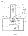
- FIG. 3 shows a charged-particle microscope 400, which, in this case, is a SEM.
- the microscope 400 comprises a particle-optical column 402, which produces a charged-particle beam 404 (in this case, an electron beam).
- the particle-optical column 402 is mounted on a vacuum chamber 406, which comprising a sample holder / stage 408 for holding a sample 410.
- the vacuum chamber 406 is evacuated using vacuum pumps (not depicted). With the aid of voltage source 422, the sample holder 408, or at least the sample 410, may be biased (floated) to an electrical potential with respect to ground.
- the particle-optical column 402 comprises an electron source 412, lenses 414, 416 to focus the electron beam 404 onto the sample 410, and a deflection unit 418.
- the apparatus is equipped with:
- stimulated radiation - comprising, for example, X-rays, infrared/visible/ultraviolet light, secondary electrons and backscatter (BS) electrons - emanates from the sample 410.
- X-rays are detected by first detector 420
- secondary electrons / BS electrons are detected by second detector 100.
- the emitted radiation is position-sensitive (due to said scanning motion)
- the information obtained from the detectors 420, 100 will also be position-dependent.
- the signals from the detectors 420,100 are processed by the processing apparatus 424, and displayed on display unit 426.
- processing may include operations such as combining, integrating, subtracting, false colouring, edge enhancing, and other processing known to the person skilled in the art.
- automated recognition processes e.g. as used for particle analysis, may be included in such processing.
- Figure 4 renders a schematic plan view (underside view) of aspects of a detector 100 suitable for use in the present invention.
- the depicted detector 100 is particularly suitable for measuring BS electrons (though it can also register secondary electrons), and does so in a so-called segmented/quadrant/concentric configuration.
- detector 100 is provided with a through-hole 112 which is centred about an axis 102 perpendicular to the drawing.
- this axis 102 will generally coincide with the optical axis of the charged-particle microscope in which the detector 100 is mounted.
- the detector 100 comprises annular detector areas 104 and 106, in nested arrangement.
- Each connection pad 206-j is connected to its corresponding detector area via a conductive track 208-j.
- the detector 100 is disposed on an n-type substrate (e.g. an n-doped silicon substrate with a typical volume resistivity of 1-10 ⁇ cm), which is metallized on one side so as to form said common backside electrode.
- an intrinsic layer (active layer) in the form of an epitaxial Si layer is formed (e.g. with a thickness of 40 ⁇ m).
- a boron layer is deposited, whereby a p + -type diffusion layer of silicon-boride layer is created.
- Enclosing the various radiation-sensitive detector areas 104, 106, 202-i, 204-i, p-doped e.g.
- boron-doped boundaries are formed.
- Said detector areas are electrically insulated from each other by an interposed n-doped implant area (e.g. with a phosphorus dopant) that, together with said p-doped areas, forms a p-n-p barrier between said detector areas.
- Part of said epitaxial layer is covered by a layer of silicon dioxide, upon which aluminium tracks are formed for the purpose of transporting the signals from said detector areas (ultimately connecting to tracks 208-j in Figure 3 ).
- a signal from each detector area 104, 106, 202-i, 204-i can be registered by measuring the current/voltage induced between said common backside electrode and the specific aluminium track of the detector area in question.
- Each detector area thus constitutes a so-called "P-I-N diode", formed by said p + -diffusion layer, intrinsic layer, and n-doped substrate. Any holes in the intrinsic layer will travel to the p + -layer, and any electrons in the intrinsic layer will travel to the n-doped substrate. Electron/hole pairs generated in the intrinsic layer will thus induce a current. Such electron/hole pairs are, for example, generated in a sample by impinging electrons (from an incoming electron beam), whereby the number of generated electron/hole pairs will be proportional to the energy with which the electrons enter the intrinsic layer and inversely proportional to the energy needed to form an electron/hole pair.
- a beam of electrons is directed along the axis 102 from the backside of the detector through the through-hole 112 onto a sample situated at the front (radiation-sensitive) side of the detector 100.
- secondary electrons and BS electrons will be liberated by the impinging electron beam.
- Secondary electrons are often categorized as electrons that emerge from the sample with an energy less than 50 eV, while BS electrons are generally categorized as electrons emerging from the sample with an energy in excess of 50 eV.
- the detector 100 is maintained at a slight positive potential with respect to said sample, by electrically biasing the sample or the detector; in this way, electrons will be accelerated towards the detector.
- secondary electrons will be detected quite close to the axis 102, as they have relatively little energy radial to the axis, whereas BS electrons will be detected by the detector areas further removed from the axis 102, as BS electrons often have more significant radial energy to start off with.
- the detector areas more distal from the axis 102 are segmented into four 90° segments. By comparing the signals induced in different such segments (and also by comparing the signal from different annuli), one can effectively angularly resolve the electrons emanating from the sample.
- Figures 5A, 5B and 5C render perspective views of detector set-ups which illustrate how emitted radiation emanating from a sample can be manipulated (deflected), in accordance with a particular aspect of the current invention.
- Each of the figures schematically depicts a disc-like sample upon which a substantially vertical incoming beam IB of charged-particle radiation is impinging.
- the sample produces a cone-like cloud of emitted radiation, which emanates from the sample substantially back in the direction of the incoming beam.
- a nested array of concentric annular zones - A, B, C, D - which are substantially centered on the incoming beam, and are substantially normal thereto.
- These zones A, B, C, D may represent various zones of a segmented detector such as that illustrated in Figure 4 , or they may simply be an abstraction serving to categorize the various emergence angles at which emitted radiation propagates from the sample.
- Figure 5A shows a "default" scenario, which is essentially symmetric and unmanipulated.
- a "default" scenario which is essentially symmetric and unmanipulated.
- the depicted scenario as illustrating symmetric impingement of the emitted radiation on the face of a detector such as that of Figure 4 , whereby concurrent detection along various emergence angles is achieved.
- Highlighted in Figure 4 is a relatively narrow cone of "paraxial" emitted radiation, which returns in close proximity to the incoming beam IB.
- This radiation falls inside zone A, and may be difficult to detect because it is so close to the optical axis of the charged-particle lens that produced the beam IB. Yet, as set forth above, because it is emitted at such a small emergence angle, this "paraxial" radiation will be emitted from (relatively) deepest within the sample, and it therefore generally contains valuable information in the context of the depth-resolution desired by the current invention. One may therefore resort to a technique to deflect this intrinsically "paraxial" region into a zone in which it can be more easily detected. Two such techniques will now be elucidated.
Landscapes
- Chemical & Material Sciences (AREA)
- Analytical Chemistry (AREA)
- Engineering & Computer Science (AREA)
- Computer Vision & Pattern Recognition (AREA)
- Physics & Mathematics (AREA)
- Health & Medical Sciences (AREA)
- Life Sciences & Earth Sciences (AREA)
- Biochemistry (AREA)
- General Health & Medical Sciences (AREA)
- General Physics & Mathematics (AREA)
- Immunology (AREA)
- Pathology (AREA)
- Analysing Materials By The Use Of Radiation (AREA)
Claims (9)
- Procédé pour examiner un échantillon (410) en utilisant un microscope à particules chargées à non transmission (400), comportant les étapes suivantes :- le montage de l'échantillon (410) sur un porte-échantillon (408) ;- l'utilisation d'une colonne optique à particules (402) pour diriger au moins un faisceau (404) d'un rayonnement de particules sur une surface S de l'échantillon (410), produisant ainsi une interaction qui amène le rayonnement émis à émaner de l'échantillon (410) ;- l'utilisation d'un agencement de détecteur (100; 420) pour détecter au moins une partie dudit rayonnement émis,- l'enregistrement d'une sortie On dudit agencement de détecteur (100 ; 420) en tant que fonction d'un angle d'émergence θn d'un rayonnement émis, mesuré par rapport à un axe normal à S, compilant ainsi un ensemble de mesures M = {(On, θn)} pour une pluralité de valeurs de θn ;- l'utilisation d'un appareil de traitement informatique (424) pour déconvoluer automatiquement l'ensemble de mesures M et le former spatialement en un ensemble de résultats R = {(Vk, Lk)}, dans lequel une variable spatiale V montre une valeur Vk à un niveau de profondeur discret associé Lk en référence à la surface S,dans lequel n et k sont des membres d'une séquence d'entiers, et la variable spatiale V représente une propriété physique de l'échantillon (410) en tant que fonction d'une position dans son ensemble, et dans lequel l'ensemble de mesures M est automatiquement traité de sorte qu'il comporte les étapes suivantes :- la définition d'une fonction d'étalement de point, pour chaque valeur de n, possède une valeur de noyau Kn représentant un comportement dudit faisceau du rayonnement de particules dans un ensemble de l'échantillon (410) tel que perçu par l'agencement de détecteur (100 ; 420) pour un angle d'émergence θn ;- la définition d'une quantité d'image qui, pour chaque valeur de n, possède une valeur Qn qui est une convolution multidimensionnelle de Kn et V, de sorte que Qn = Kn *V ;- pour chaque valeur de n, la détermination par calcul d'une divergence minimum

entre On et Qn dans lequel on calcule V tout en appliquant des contraintes sur les valeurs Kn. - Procédé selon la revendication 1, dans lequel :- ledit agencement de détecteur (100 ; 420) comprend une pluralité de sous-détecteurs {Dn} qui sont angulairement répartis sur ledit porte-échantillon (408) ;- l'ensemble de mesures M est compilé en acquérant simultanément ses paires de données de composante (On, θn), moyennant quoi chaque sous-détecteur individuel Dn capture le rayonnement émis à l'angle associé θn et produit une valeur de sortie associée On.
- Procédé selon la revendication 1, dans lequel :- ledit agencement de détecteur (100 ; 420) comprend un détecteur unitaire et un assemblage de déflecteur, ledit assemblage de déflecteur étant réglable de manière à adopter un ensemble de positions de déflection A = {An}, chaque position de déflecteur An servant à sélectionner un angle θn dont le rayonnement émis associé doit être présenté au détecteur unitaire ;- l'ensemble de mesures M est compilé en acquérant séquentiellement ses paires de données de composante (On, θn), moyennant quoi chaque position An permet au détecteur unitaire de capturer une paire de données associées (On, θn).
- Procédé selon la revendication 3, dans lequel ledit assemblage de déflecteur est sélectionné parmi le groupe comprenant :- des moyens pour changer localement la direction du rayonnement émis émanant de l'échantillon (410) ;- des moyens pour incliner le porte-échantillon (408) par rapport au détecteur unitaire ;- des moyens pour déplacer angulairement le détecteur unitaire par rapport à l'échantillon (410),et des combinaisons de ceux-ci.
- Procédé selon l'une quelconque des revendications précédentes, dans lequel ledit rayonnement émis est sélectionné parmi le groupe comprenant des électrons rétrodiffusés, des rayons X, une lumière infrarouge, une lumière visible, une lumière ultraviolette, et des combinaisons de ceux-ci.
- Procédé selon l'une quelconque des revendications précédentes, dans lequel ladite divergence est supposée soumise à au moins l'un d'un bruit de Poisson et d'un bruit de Gauss.
- Procédé selon l'une quelconque des revendications précédentes, dans lequel :- lesdites étapes de compilation d'un ensemble de mesures M et de conversion mathématique de celle-ci en un ensemble de résultats correspondants R sont comprises dans une étape de tranchage de calcul ;- ladite étape d'écrêtage informatique est combinée à une étape de tranchage physique, moyennant quoi un procédé de suppression de matériau physique est utilisé pour supprimer physiquement une couche de matériau de la surface d'origine de l'échantillon (410), révélant ainsi une surface nouvellement exposée de l'échantillon (410).
- Microscope à particules chargées (400) réalisé et agencé pour effectuer un procédé selon l'une quelconque des revendications 1-7.
- Microscope à particules chargées (400) selon la revendication 8, lequel microscope est un microscope électronique à balayage (MEB).
Priority Applications (1)
| Application Number | Priority Date | Filing Date | Title |
|---|---|---|---|
| EP12179764.1A EP2557587B1 (fr) | 2011-08-10 | 2012-08-09 | Microscope à particules chargées fournissant une imagerie à résolution en profondeur |
Applications Claiming Priority (3)
| Application Number | Priority Date | Filing Date | Title |
|---|---|---|---|
| EP11177091A EP2557584A1 (fr) | 2011-08-10 | 2011-08-10 | Procédé d'imagerie par microscopie à particules chargées |
| EP12163262A EP2557585A1 (fr) | 2011-08-10 | 2012-04-05 | Microscope à particules chargées fournissant une imagerie à résolution en profondeur |
| EP12179764.1A EP2557587B1 (fr) | 2011-08-10 | 2012-08-09 | Microscope à particules chargées fournissant une imagerie à résolution en profondeur |
Publications (3)
| Publication Number | Publication Date |
|---|---|
| EP2557587A2 EP2557587A2 (fr) | 2013-02-13 |
| EP2557587A3 EP2557587A3 (fr) | 2013-04-10 |
| EP2557587B1 true EP2557587B1 (fr) | 2015-10-07 |
Family
ID=45894711
Family Applications (5)
| Application Number | Title | Priority Date | Filing Date |
|---|---|---|---|
| EP11177091A Withdrawn EP2557584A1 (fr) | 2011-08-10 | 2011-08-10 | Procédé d'imagerie par microscopie à particules chargées |
| EP12163262A Withdrawn EP2557585A1 (fr) | 2011-08-10 | 2012-04-05 | Microscope à particules chargées fournissant une imagerie à résolution en profondeur |
| EP12179764.1A Active EP2557587B1 (fr) | 2011-08-10 | 2012-08-09 | Microscope à particules chargées fournissant une imagerie à résolution en profondeur |
| EP12179763.3A Active EP2557586B1 (fr) | 2011-08-10 | 2012-08-09 | Procédé d'imagerie par microscopie à particules chargées |
| EP13153164.2A Withdrawn EP2648207A1 (fr) | 2011-08-10 | 2013-01-30 | Microscope à particules chargées fournissant une imagerie à résolution en profondeur |
Family Applications Before (2)
| Application Number | Title | Priority Date | Filing Date |
|---|---|---|---|
| EP11177091A Withdrawn EP2557584A1 (fr) | 2011-08-10 | 2011-08-10 | Procédé d'imagerie par microscopie à particules chargées |
| EP12163262A Withdrawn EP2557585A1 (fr) | 2011-08-10 | 2012-04-05 | Microscope à particules chargées fournissant une imagerie à résolution en profondeur |
Family Applications After (2)
| Application Number | Title | Priority Date | Filing Date |
|---|---|---|---|
| EP12179763.3A Active EP2557586B1 (fr) | 2011-08-10 | 2012-08-09 | Procédé d'imagerie par microscopie à particules chargées |
| EP13153164.2A Withdrawn EP2648207A1 (fr) | 2011-08-10 | 2013-01-30 | Microscope à particules chargées fournissant une imagerie à résolution en profondeur |
Country Status (4)
| Country | Link |
|---|---|
| US (2) | US8581189B2 (fr) |
| EP (5) | EP2557584A1 (fr) |
| JP (2) | JP6195699B2 (fr) |
| CN (2) | CN102954773B (fr) |
Cited By (4)
| Publication number | Priority date | Publication date | Assignee | Title |
|---|---|---|---|---|
| EP3297018A1 (fr) | 2016-09-19 | 2018-03-21 | FEI Company | Procédé d'imagerie tomographique |
| US12456600B2 (en) | 2023-05-29 | 2025-10-28 | Applied Materials Israel Ltd. | Scanning electron microscopy-based tomography of specimens |
| US12480898B2 (en) | 2022-09-01 | 2025-11-25 | Applied Materials Israel Ltd. | Z-profiling of wafers based on X-ray measurements |
| US12625098B2 (en) | 2023-01-30 | 2026-05-12 | Applied Materials Israel Ltd. | Non-destructive classification of specimens based on energy signature measurements |
Families Citing this family (42)
| Publication number | Priority date | Publication date | Assignee | Title |
|---|---|---|---|---|
| US8476585B2 (en) * | 2011-03-02 | 2013-07-02 | Gatan, Inc. | Microtome utilizing a movable knife in a retardation field scanning electron microscope and a retardation field scanning electron microscope including the same |
| EP2605005A1 (fr) * | 2011-12-14 | 2013-06-19 | FEI Company | Groupage de données multimodales |
| EP2557584A1 (fr) * | 2011-08-10 | 2013-02-13 | Fei Company | Procédé d'imagerie par microscopie à particules chargées |
| US8704176B2 (en) | 2011-08-10 | 2014-04-22 | Fei Company | Charged particle microscope providing depth-resolved imagery |
| FR2979165B1 (fr) * | 2011-08-16 | 2014-05-16 | Commissariat Energie Atomique | Procede de correction des effets de proximite electronique utilisant des fonctions de diffusion decentrees |
| EP2648208B1 (fr) * | 2012-04-05 | 2017-08-09 | Fei Company | Microscope à particules chargées fournissant une imagerie à résolution en profondeur |
| EP2708874A1 (fr) | 2012-09-12 | 2014-03-19 | Fei Company | Procédé permettant de réaliser une imagerie tomographique d'un échantillon dans un microscope à faisceau de particules chargées |
| DE102012217761B4 (de) * | 2012-09-28 | 2020-02-06 | Carl Zeiss Microscopy Gmbh | Verfahren zur Vermeidung von Artefakten beim Serial Block Face Imaging |
| EP2735866A1 (fr) | 2012-11-27 | 2014-05-28 | Fei Company | Procédé de prélèvement d'un échantillon et d'affichage d'informations obtenues |
| EP2738786A1 (fr) | 2012-11-29 | 2014-06-04 | Fei Company | Procédé permettant de réaliser une imagerie tomographique d'un échantillon dans un microscope à faisceau de particules chargées |
| TWI461653B (zh) * | 2013-02-06 | 2014-11-21 | Inotera Memories Inc | 測量樣本尺寸的方法 |
| GB201302624D0 (en) * | 2013-02-14 | 2013-04-03 | Univ Antwerpen | High-resolution amplitude contrast imaging |
| US9190241B2 (en) * | 2013-03-25 | 2015-11-17 | Hermes-Microvision, Inc. | Charged particle beam apparatus |
| US9177758B2 (en) * | 2013-03-25 | 2015-11-03 | Hermes Microvision Inc. | Charged particle beam apparatus |
| JP2014216213A (ja) * | 2013-04-26 | 2014-11-17 | 株式会社日立ハイテクノロジーズ | 荷電粒子顕微鏡装置および荷電粒子顕微鏡装置の画像取得方法 |
| EP2824445B1 (fr) * | 2013-07-08 | 2016-03-02 | Fei Company | Microscopie à particules chargées combinée avec spectroscopie raman |
| EP2958130A1 (fr) | 2014-06-18 | 2015-12-23 | Fei Company | Reconstruction d'image mathématique dans un microscope de type balayage |
| EP2963672A1 (fr) | 2014-06-30 | 2016-01-06 | FEI Company | Microscopie à balayage assistée par ordinateur à résolution améliorée |
| US9627175B2 (en) * | 2014-10-17 | 2017-04-18 | Jeol Ltd. | Electron microscope and elemental mapping image generation method |
| DE102014226985B4 (de) | 2014-12-23 | 2024-02-08 | Carl Zeiss Microscopy Gmbh | Verfahren zum Analysieren eines Objekts, Computerprogrammprodukt sowie Teilchenstrahlgerät zur Durchführung des Verfahrens |
| US9842724B2 (en) * | 2015-02-03 | 2017-12-12 | Kla-Tencor Corporation | Method and system for imaging of a photomask through a pellicle |
| US10236156B2 (en) | 2015-03-25 | 2019-03-19 | Hermes Microvision Inc. | Apparatus of plural charged-particle beams |
| EP3082150B1 (fr) * | 2015-04-15 | 2017-07-19 | FEI Company | Procédé et microscope à particules chargées à balayage en transmission pour imagerie tomographique |
| US9502211B1 (en) | 2015-05-03 | 2016-11-22 | Fei Company | Adaptive scanning for particle size using directed beam signal analysis |
| US10056224B2 (en) * | 2015-08-10 | 2018-08-21 | Kla-Tencor Corporation | Method and system for edge-of-wafer inspection and review |
| JP6527799B2 (ja) | 2015-09-25 | 2019-06-05 | 株式会社日立ハイテクノロジーズ | 荷電粒子線装置及びパターン測定装置 |
| EP3174085A1 (fr) | 2015-11-30 | 2017-05-31 | FEI Company | Ensemble filtre pour discrimination entre des électrons secondaires et des électrons rétrodiffusés dans un microscope à particules chargées de non-transmission |
| EP3486633B1 (fr) * | 2015-12-11 | 2021-11-24 | FEI Company | Préparation d'un échantillon cryogénique pour la microscopie à particules chargées |
| EP3240013B1 (fr) * | 2016-04-26 | 2018-11-07 | FEI Company | Imagerie tridimensionnelle dans la microscopie à particules chargées |
| DE102016208689B4 (de) | 2016-05-20 | 2018-07-26 | Carl Zeiss Microscopy Gmbh | Verfahren zum Erzeugen eines Bildes eines Objekts und/oder einer Darstellung von Daten über das Objekt sowie Computerprogrammprodukt und Teilchenstrahlgerät zur Durchführung des Verfahrens |
| US11205103B2 (en) | 2016-12-09 | 2021-12-21 | The Research Foundation for the State University | Semisupervised autoencoder for sentiment analysis |
| US10840056B2 (en) * | 2017-02-03 | 2020-11-17 | Kla Corporation | Multi-column scanning electron microscopy system |
| JP6796813B2 (ja) | 2017-02-10 | 2020-12-09 | パナソニックIpマネジメント株式会社 | 応力測定システムおよび応力測定方法 |
| DE102017119531A1 (de) * | 2017-08-25 | 2019-02-28 | Carl Zeiss Microscopy Gmbh | Hochauflösende 2D-Mikroskopie mit verbesserter Schnittdicke |
| EP3499459A1 (fr) | 2017-12-18 | 2019-06-19 | FEI Company | Procédé, dispositif et système d'apprentissage profond à distance pour la segmentation et la reconstruction d'images microscopiques |
| DE102018007455B4 (de) * | 2018-09-21 | 2020-07-09 | Carl Zeiss Multisem Gmbh | Verfahren zum Detektorabgleich bei der Abbildung von Objekten mittels eines Mehrstrahl-Teilchenmikroskops, System sowie Computerprogrammprodukt |
| US10872746B2 (en) * | 2018-11-02 | 2020-12-22 | Decision Sciences International Corporation | System of mobile charged particle detectors and methods of spent nuclear fuel imaging |
| US20200312611A1 (en) | 2019-03-29 | 2020-10-01 | Fei Company | Artificial intelligence enabled volume reconstruction |
| EP3745442A1 (fr) * | 2019-05-29 | 2020-12-02 | FEI Company | Procédé d'examen d'un échantillon à l'aide d'un microscope à particules chargées |
| CN110162904B (zh) * | 2019-05-29 | 2023-03-10 | 哈尔滨工业大学(深圳) | 金属-介电多层柱状光学纳米天线的贝叶斯优化设计方法 |
| DE102019133658A1 (de) | 2019-12-10 | 2021-06-10 | Carl Zeiss Smt Gmbh | Vorrichtung und Verfahren zum Bearbeiten einer mikrostrukturierten Komponente |
| JP2025504235A (ja) * | 2022-02-10 | 2025-02-06 | カール・ツァイス・エスエムティー・ゲーエムベーハー | 半導体試料を層ごとに検査するための方法およびそのような方法を実行するための検査装置 |
Family Cites Families (29)
| Publication number | Priority date | Publication date | Assignee | Title |
|---|---|---|---|---|
| JPS56141155A (en) * | 1980-04-04 | 1981-11-04 | Hitachi Ltd | Analyzed sample position setter |
| JPH0676975B2 (ja) * | 1984-09-26 | 1994-09-28 | 新技術事業団 | 表面原子配列構造の観察方法 |
| JPH0233845A (ja) * | 1988-07-22 | 1990-02-05 | Nec Corp | 走査型電子顕微鏡 |
| US5412210A (en) | 1990-10-12 | 1995-05-02 | Hitachi, Ltd. | Scanning electron microscope and method for production of semiconductor device by using the same |
| JPH08329875A (ja) * | 1995-06-01 | 1996-12-13 | Hitachi Ltd | 走査型電子顕微鏡及びその試料像表示方法 |
| DE19828476A1 (de) * | 1998-06-26 | 1999-12-30 | Leo Elektronenmikroskopie Gmbh | Teilchenstrahlgerät |
| FI105438B (fi) | 1998-09-21 | 2000-08-15 | Nokia Networks Oy | Yhteydenmuodostus langattomassa tietoliikenneverkossa |
| EP0989141A1 (fr) | 1998-09-25 | 2000-03-29 | Fina Research S.A. | Elaboration de polyéthylène multimodal |
| DE19946317C1 (de) | 1999-09-28 | 2001-03-01 | Sedra Asphalt Technik Biebrich | Verfahren zur Herstellung eines schallgedämmten Gleises |
| EP1209737B2 (fr) * | 2000-11-06 | 2014-04-30 | Hitachi, Ltd. | Méthode de fabrication d'un échantillon |
| JP2002310959A (ja) * | 2001-04-16 | 2002-10-23 | Shimadzu Corp | 電子線分析装置 |
| US20030132382A1 (en) * | 2001-12-18 | 2003-07-17 | Sogard Michael R. | System and method for inspecting a mask |
| KR101041661B1 (ko) * | 2003-07-30 | 2011-06-14 | 어플라이드 머티리얼즈 이스라엘 리미티드 | 다중 검출기들을 갖는 스캐닝 전자 현미경 및 다중 검출기기반 이미징을 위한 방법 |
| US20060043291A1 (en) * | 2004-08-26 | 2006-03-02 | Peng Gang G | Electron spectroscopic metrology system |
| US7411188B2 (en) * | 2005-07-11 | 2008-08-12 | Revera Incorporated | Method and system for non-destructive distribution profiling of an element in a film |
| NL1029847C2 (nl) * | 2005-09-01 | 2007-03-05 | Fei Co | Werkwijze voor het bepalen van lensfouten in een deeltjes-optisch apparaat. |
| JP4728186B2 (ja) * | 2006-07-20 | 2011-07-20 | シャープ株式会社 | 斜出射電子線プローブマイクロx線分析方法およびそれに用いられるプログラム、並びに、斜出射電子線プローブマイクロx線分析装置 |
| EP1890136A1 (fr) * | 2006-08-16 | 2008-02-20 | FEI Company | Procédé pour obtenir des images d'un échantillion tranché |
| JP2008177064A (ja) * | 2007-01-19 | 2008-07-31 | Hitachi High-Technologies Corp | 走査型荷電粒子顕微鏡装置および走査型荷電粒子顕微鏡装置で取得した画像の処理方法 |
| US7777185B2 (en) * | 2007-09-25 | 2010-08-17 | Ut-Battelle, Llc | Method and apparatus for a high-resolution three dimensional confocal scanning transmission electron microscope |
| JP5164754B2 (ja) * | 2008-09-08 | 2013-03-21 | 株式会社日立ハイテクノロジーズ | 走査型荷電粒子顕微鏡装置及び走査型荷電粒子顕微鏡装置で取得した画像の処理方法 |
| CN101768008B (zh) * | 2009-01-06 | 2012-10-03 | 中国科学院金属研究所 | 结构复杂材料的三维倒易空间重构方法 |
| EP2346094A1 (fr) | 2010-01-13 | 2011-07-20 | FEI Company | Procédé de fabrication d'un détecteur de rayonnements |
| JP5764380B2 (ja) * | 2010-04-29 | 2015-08-19 | エフ イー アイ カンパニFei Company | Sem画像化法 |
| EP2461348A1 (fr) | 2010-12-06 | 2012-06-06 | FEI Company | Système de détecteur à utiliser avec une spectroscopie de microscope électronique à transmission |
| US8669524B2 (en) * | 2010-10-25 | 2014-03-11 | The Reseach Foundation of State University of New York | Scanning incremental focus microscopy |
| US9679741B2 (en) * | 2010-11-09 | 2017-06-13 | Fei Company | Environmental cell for charged particle beam system |
| EP2525385A1 (fr) | 2011-05-16 | 2012-11-21 | Fei Company | Microscope à particules chargées |
| EP2557584A1 (fr) * | 2011-08-10 | 2013-02-13 | Fei Company | Procédé d'imagerie par microscopie à particules chargées |
-
2011
- 2011-08-10 EP EP11177091A patent/EP2557584A1/fr not_active Withdrawn
-
2012
- 2012-04-05 EP EP12163262A patent/EP2557585A1/fr not_active Withdrawn
- 2012-08-09 EP EP12179764.1A patent/EP2557587B1/fr active Active
- 2012-08-09 EP EP12179763.3A patent/EP2557586B1/fr active Active
- 2012-08-09 JP JP2012176834A patent/JP6195699B2/ja active Active
- 2012-08-09 JP JP2012176833A patent/JP6099900B2/ja active Active
- 2012-08-10 US US13/572,206 patent/US8581189B2/en active Active
- 2012-08-10 CN CN201210283575.XA patent/CN102954773B/zh active Active
- 2012-08-10 CN CN201210283730.8A patent/CN102931044B/zh active Active
- 2012-08-10 US US13/572,449 patent/US8586921B2/en active Active
-
2013
- 2013-01-30 EP EP13153164.2A patent/EP2648207A1/fr not_active Withdrawn
Non-Patent Citations (2)
| Title |
|---|
| ANONYMOUS: "3D reconstruction from multiple images - Wikipedia, the free encyclopedia", 9 February 2012 (2012-02-09), XP055110940, Retrieved from the Internet <URL:http://en.wikipedia.org/w/index.php?title=3D_reconstruction_from_multiple_images&oldid=475965681> [retrieved on 20140331] * |
| TCHELIDZE P ET AL: "Electron tomography of amplified nanogold immunolabelling: Improvement of quality based on alignment of projections with sinograms and use of post-reconstruction deconvolution", JOURNAL OF STRUCTURAL BIOLOGY, ACADEMIC PRESS, UNITED STATES, vol. 156, no. 3, 1 December 2006 (2006-12-01), pages 421 - 431, XP024905319, ISSN: 1047-8477, [retrieved on 20061201], DOI: 10.1016/J.JSB.2006.07.004 * |
Cited By (4)
| Publication number | Priority date | Publication date | Assignee | Title |
|---|---|---|---|---|
| EP3297018A1 (fr) | 2016-09-19 | 2018-03-21 | FEI Company | Procédé d'imagerie tomographique |
| US12480898B2 (en) | 2022-09-01 | 2025-11-25 | Applied Materials Israel Ltd. | Z-profiling of wafers based on X-ray measurements |
| US12625098B2 (en) | 2023-01-30 | 2026-05-12 | Applied Materials Israel Ltd. | Non-destructive classification of specimens based on energy signature measurements |
| US12456600B2 (en) | 2023-05-29 | 2025-10-28 | Applied Materials Israel Ltd. | Scanning electron microscopy-based tomography of specimens |
Also Published As
| Publication number | Publication date |
|---|---|
| US20130037714A1 (en) | 2013-02-14 |
| US8581189B2 (en) | 2013-11-12 |
| JP6099900B2 (ja) | 2017-03-22 |
| US20130037715A1 (en) | 2013-02-14 |
| CN102954773A (zh) | 2013-03-06 |
| EP2557586A3 (fr) | 2013-04-10 |
| CN102931044B (zh) | 2016-09-21 |
| EP2557585A1 (fr) | 2013-02-13 |
| EP2557587A3 (fr) | 2013-04-10 |
| EP2557586B1 (fr) | 2014-04-02 |
| EP2557584A1 (fr) | 2013-02-13 |
| JP6195699B2 (ja) | 2017-09-13 |
| CN102954773B (zh) | 2016-12-21 |
| CN102931044A (zh) | 2013-02-13 |
| JP2013037001A (ja) | 2013-02-21 |
| EP2557587A2 (fr) | 2013-02-13 |
| EP2557586A2 (fr) | 2013-02-13 |
| US8586921B2 (en) | 2013-11-19 |
| EP2648207A1 (fr) | 2013-10-09 |
| JP2013037000A (ja) | 2013-02-21 |
Similar Documents
| Publication | Publication Date | Title |
|---|---|---|
| US8586921B2 (en) | Charged-particle microscope providing depth-resolved imagery | |
| US9711325B2 (en) | Charged-particle microscope providing depth-resolved imagery | |
| EP2963673B1 (fr) | Microscopie a balayage de calcul a resolution amelioree | |
| US9812287B2 (en) | Charged particle microscope with improved spectroscopic functionality | |
| CN106057620B (zh) | 在带电粒子显微镜中执行层析成像的方法 | |
| EP2525386B1 (fr) | Microscopie à particules chargées avec détection d'occlusion | |
| EP2648208B1 (fr) | Microscope à particules chargées fournissant une imagerie à résolution en profondeur | |
| JP7007136B2 (ja) | トモグラフィック・イメージング方法 | |
| CN103367085B (zh) | 提供深度分辨图像的带电粒子显微镜 | |
| KR102565911B1 (ko) | 하전 입자 현미경에서의 공초점 이미징 기술 | |
| Bosch | Boughorbel et a1. |
Legal Events
| Date | Code | Title | Description |
|---|---|---|---|
| PUAI | Public reference made under article 153(3) epc to a published international application that has entered the european phase |
Free format text: ORIGINAL CODE: 0009012 |
|
| AK | Designated contracting states |
Kind code of ref document: A2 Designated state(s): AL AT BE BG CH CY CZ DE DK EE ES FI FR GB GR HR HU IE IS IT LI LT LU LV MC MK MT NL NO PL PT RO RS SE SI SK SM TR |
|
| AX | Request for extension of the european patent |
Extension state: BA ME |
|
| PUAL | Search report despatched |
Free format text: ORIGINAL CODE: 0009013 |
|
| AK | Designated contracting states |
Kind code of ref document: A3 Designated state(s): AL AT BE BG CH CY CZ DE DK EE ES FI FR GB GR HR HU IE IS IT LI LT LU LV MC MK MT NL NO PL PT RO RS SE SI SK SM TR |
|
| AX | Request for extension of the european patent |
Extension state: BA ME |
|
| RIC1 | Information provided on ipc code assigned before grant |
Ipc: H01J 37/28 20060101ALI20130301BHEP Ipc: H01J 37/22 20060101AFI20130301BHEP |
|
| 17P | Request for examination filed |
Effective date: 20130531 |
|
| RBV | Designated contracting states (corrected) |
Designated state(s): AL AT BE BG CH CY CZ DE DK EE ES FI FR GB GR HR HU IE IS IT LI LT LU LV MC MK MT NL NO PL PT RO RS SE SI SK SM TR |
|
| 17Q | First examination report despatched |
Effective date: 20140422 |
|
| GRAP | Despatch of communication of intention to grant a patent |
Free format text: ORIGINAL CODE: EPIDOSNIGR1 |
|
| RIC1 | Information provided on ipc code assigned before grant |
Ipc: H01J 37/22 20060101AFI20150407BHEP Ipc: G01N 23/22 20060101ALI20150407BHEP Ipc: H01J 37/28 20060101ALI20150407BHEP |
|
| INTG | Intention to grant announced |
Effective date: 20150429 |
|
| RIN1 | Information on inventor provided before grant (corrected) |
Inventor name: POTOCEK, PAVEL Inventor name: LICH, BEN Inventor name: BOUGHORBEL, FAYSAL Inventor name: KOOIJMAN, CEES |
|
| GRAS | Grant fee paid |
Free format text: ORIGINAL CODE: EPIDOSNIGR3 |
|
| GRAA | (expected) grant |
Free format text: ORIGINAL CODE: 0009210 |
|
| AK | Designated contracting states |
Kind code of ref document: B1 Designated state(s): AL AT BE BG CH CY CZ DE DK EE ES FI FR GB GR HR HU IE IS IT LI LT LU LV MC MK MT NL NO PL PT RO RS SE SI SK SM TR |
|
| REG | Reference to a national code |
Ref country code: GB Ref legal event code: FG4D |
|
| REG | Reference to a national code |
Ref country code: AT Ref legal event code: REF Ref document number: 754192 Country of ref document: AT Kind code of ref document: T Effective date: 20151015 Ref country code: CH Ref legal event code: EP |
|
| REG | Reference to a national code |
Ref country code: IE Ref legal event code: FG4D |
|
| REG | Reference to a national code |
Ref country code: DE Ref legal event code: R096 Ref document number: 602012011280 Country of ref document: DE |
|
| REG | Reference to a national code |
Ref country code: NL Ref legal event code: MP Effective date: 20151007 |
|
| REG | Reference to a national code |
Ref country code: AT Ref legal event code: MK05 Ref document number: 754192 Country of ref document: AT Kind code of ref document: T Effective date: 20151007 |
|
| REG | Reference to a national code |
Ref country code: LT Ref legal event code: MG4D |
|
| PG25 | Lapsed in a contracting state [announced via postgrant information from national office to epo] |
Ref country code: IS Free format text: LAPSE BECAUSE OF FAILURE TO SUBMIT A TRANSLATION OF THE DESCRIPTION OR TO PAY THE FEE WITHIN THE PRESCRIBED TIME-LIMIT Effective date: 20160207 Ref country code: NL Free format text: LAPSE BECAUSE OF FAILURE TO SUBMIT A TRANSLATION OF THE DESCRIPTION OR TO PAY THE FEE WITHIN THE PRESCRIBED TIME-LIMIT Effective date: 20151007 Ref country code: NO Free format text: LAPSE BECAUSE OF FAILURE TO SUBMIT A TRANSLATION OF THE DESCRIPTION OR TO PAY THE FEE WITHIN THE PRESCRIBED TIME-LIMIT Effective date: 20160107 Ref country code: HR Free format text: LAPSE BECAUSE OF FAILURE TO SUBMIT A TRANSLATION OF THE DESCRIPTION OR TO PAY THE FEE WITHIN THE PRESCRIBED TIME-LIMIT Effective date: 20151007 Ref country code: LT Free format text: LAPSE BECAUSE OF FAILURE TO SUBMIT A TRANSLATION OF THE DESCRIPTION OR TO PAY THE FEE WITHIN THE PRESCRIBED TIME-LIMIT Effective date: 20151007 Ref country code: ES Free format text: LAPSE BECAUSE OF FAILURE TO SUBMIT A TRANSLATION OF THE DESCRIPTION OR TO PAY THE FEE WITHIN THE PRESCRIBED TIME-LIMIT Effective date: 20151007 Ref country code: IT Free format text: LAPSE BECAUSE OF FAILURE TO SUBMIT A TRANSLATION OF THE DESCRIPTION OR TO PAY THE FEE WITHIN THE PRESCRIBED TIME-LIMIT Effective date: 20151007 |
|
| PG25 | Lapsed in a contracting state [announced via postgrant information from national office to epo] |
Ref country code: GR Free format text: LAPSE BECAUSE OF FAILURE TO SUBMIT A TRANSLATION OF THE DESCRIPTION OR TO PAY THE FEE WITHIN THE PRESCRIBED TIME-LIMIT Effective date: 20160108 Ref country code: RS Free format text: LAPSE BECAUSE OF FAILURE TO SUBMIT A TRANSLATION OF THE DESCRIPTION OR TO PAY THE FEE WITHIN THE PRESCRIBED TIME-LIMIT Effective date: 20151007 Ref country code: PT Free format text: LAPSE BECAUSE OF FAILURE TO SUBMIT A TRANSLATION OF THE DESCRIPTION OR TO PAY THE FEE WITHIN THE PRESCRIBED TIME-LIMIT Effective date: 20160208 Ref country code: AT Free format text: LAPSE BECAUSE OF FAILURE TO SUBMIT A TRANSLATION OF THE DESCRIPTION OR TO PAY THE FEE WITHIN THE PRESCRIBED TIME-LIMIT Effective date: 20151007 Ref country code: FI Free format text: LAPSE BECAUSE OF FAILURE TO SUBMIT A TRANSLATION OF THE DESCRIPTION OR TO PAY THE FEE WITHIN THE PRESCRIBED TIME-LIMIT Effective date: 20151007 Ref country code: SE Free format text: LAPSE BECAUSE OF FAILURE TO SUBMIT A TRANSLATION OF THE DESCRIPTION OR TO PAY THE FEE WITHIN THE PRESCRIBED TIME-LIMIT Effective date: 20151007 Ref country code: LV Free format text: LAPSE BECAUSE OF FAILURE TO SUBMIT A TRANSLATION OF THE DESCRIPTION OR TO PAY THE FEE WITHIN THE PRESCRIBED TIME-LIMIT Effective date: 20151007 Ref country code: PL Free format text: LAPSE BECAUSE OF FAILURE TO SUBMIT A TRANSLATION OF THE DESCRIPTION OR TO PAY THE FEE WITHIN THE PRESCRIBED TIME-LIMIT Effective date: 20151007 |
|
| REG | Reference to a national code |
Ref country code: DE Ref legal event code: R097 Ref document number: 602012011280 Country of ref document: DE |
|
| PG25 | Lapsed in a contracting state [announced via postgrant information from national office to epo] |
Ref country code: CZ Free format text: LAPSE BECAUSE OF FAILURE TO SUBMIT A TRANSLATION OF THE DESCRIPTION OR TO PAY THE FEE WITHIN THE PRESCRIBED TIME-LIMIT Effective date: 20151007 |
|
| PLBE | No opposition filed within time limit |
Free format text: ORIGINAL CODE: 0009261 |
|
| STAA | Information on the status of an ep patent application or granted ep patent |
Free format text: STATUS: NO OPPOSITION FILED WITHIN TIME LIMIT |
|
| REG | Reference to a national code |
Ref country code: FR Ref legal event code: PLFP Year of fee payment: 5 |
|
| PG25 | Lapsed in a contracting state [announced via postgrant information from national office to epo] |
Ref country code: SM Free format text: LAPSE BECAUSE OF FAILURE TO SUBMIT A TRANSLATION OF THE DESCRIPTION OR TO PAY THE FEE WITHIN THE PRESCRIBED TIME-LIMIT Effective date: 20151007 Ref country code: SK Free format text: LAPSE BECAUSE OF FAILURE TO SUBMIT A TRANSLATION OF THE DESCRIPTION OR TO PAY THE FEE WITHIN THE PRESCRIBED TIME-LIMIT Effective date: 20151007 Ref country code: RO Free format text: LAPSE BECAUSE OF FAILURE TO SUBMIT A TRANSLATION OF THE DESCRIPTION OR TO PAY THE FEE WITHIN THE PRESCRIBED TIME-LIMIT Effective date: 20151007 Ref country code: DK Free format text: LAPSE BECAUSE OF FAILURE TO SUBMIT A TRANSLATION OF THE DESCRIPTION OR TO PAY THE FEE WITHIN THE PRESCRIBED TIME-LIMIT Effective date: 20151007 Ref country code: EE Free format text: LAPSE BECAUSE OF FAILURE TO SUBMIT A TRANSLATION OF THE DESCRIPTION OR TO PAY THE FEE WITHIN THE PRESCRIBED TIME-LIMIT Effective date: 20151007 |
|
| 26N | No opposition filed |
Effective date: 20160708 |
|
| PG25 | Lapsed in a contracting state [announced via postgrant information from national office to epo] |
Ref country code: SI Free format text: LAPSE BECAUSE OF FAILURE TO SUBMIT A TRANSLATION OF THE DESCRIPTION OR TO PAY THE FEE WITHIN THE PRESCRIBED TIME-LIMIT Effective date: 20151007 |
|
| PG25 | Lapsed in a contracting state [announced via postgrant information from national office to epo] |
Ref country code: BE Free format text: LAPSE BECAUSE OF FAILURE TO SUBMIT A TRANSLATION OF THE DESCRIPTION OR TO PAY THE FEE WITHIN THE PRESCRIBED TIME-LIMIT Effective date: 20151007 |
|
| PG25 | Lapsed in a contracting state [announced via postgrant information from national office to epo] |
Ref country code: MC Free format text: LAPSE BECAUSE OF FAILURE TO SUBMIT A TRANSLATION OF THE DESCRIPTION OR TO PAY THE FEE WITHIN THE PRESCRIBED TIME-LIMIT Effective date: 20151007 |
|
| REG | Reference to a national code |
Ref country code: CH Ref legal event code: PL |
|
| PG25 | Lapsed in a contracting state [announced via postgrant information from national office to epo] |
Ref country code: LI Free format text: LAPSE BECAUSE OF NON-PAYMENT OF DUE FEES Effective date: 20160831 Ref country code: CH Free format text: LAPSE BECAUSE OF NON-PAYMENT OF DUE FEES Effective date: 20160831 |
|
| REG | Reference to a national code |
Ref country code: IE Ref legal event code: MM4A |
|
| REG | Reference to a national code |
Ref country code: FR Ref legal event code: PLFP Year of fee payment: 6 |
|
| PG25 | Lapsed in a contracting state [announced via postgrant information from national office to epo] |
Ref country code: IE Free format text: LAPSE BECAUSE OF NON-PAYMENT OF DUE FEES Effective date: 20160809 |
|
| PG25 | Lapsed in a contracting state [announced via postgrant information from national office to epo] |
Ref country code: LU Free format text: LAPSE BECAUSE OF NON-PAYMENT OF DUE FEES Effective date: 20160809 |
|
| PG25 | Lapsed in a contracting state [announced via postgrant information from national office to epo] |
Ref country code: CY Free format text: LAPSE BECAUSE OF FAILURE TO SUBMIT A TRANSLATION OF THE DESCRIPTION OR TO PAY THE FEE WITHIN THE PRESCRIBED TIME-LIMIT Effective date: 20151007 Ref country code: HU Free format text: LAPSE BECAUSE OF FAILURE TO SUBMIT A TRANSLATION OF THE DESCRIPTION OR TO PAY THE FEE WITHIN THE PRESCRIBED TIME-LIMIT; INVALID AB INITIO Effective date: 20120809 |
|
| PG25 | Lapsed in a contracting state [announced via postgrant information from national office to epo] |
Ref country code: MK Free format text: LAPSE BECAUSE OF FAILURE TO SUBMIT A TRANSLATION OF THE DESCRIPTION OR TO PAY THE FEE WITHIN THE PRESCRIBED TIME-LIMIT Effective date: 20151007 Ref country code: TR Free format text: LAPSE BECAUSE OF FAILURE TO SUBMIT A TRANSLATION OF THE DESCRIPTION OR TO PAY THE FEE WITHIN THE PRESCRIBED TIME-LIMIT Effective date: 20151007 Ref country code: MT Free format text: LAPSE BECAUSE OF NON-PAYMENT OF DUE FEES Effective date: 20160831 |
|
| REG | Reference to a national code |
Ref country code: FR Ref legal event code: PLFP Year of fee payment: 7 |
|
| PG25 | Lapsed in a contracting state [announced via postgrant information from national office to epo] |
Ref country code: BG Free format text: LAPSE BECAUSE OF FAILURE TO SUBMIT A TRANSLATION OF THE DESCRIPTION OR TO PAY THE FEE WITHIN THE PRESCRIBED TIME-LIMIT Effective date: 20151007 |
|
| PG25 | Lapsed in a contracting state [announced via postgrant information from national office to epo] |
Ref country code: AL Free format text: LAPSE BECAUSE OF FAILURE TO SUBMIT A TRANSLATION OF THE DESCRIPTION OR TO PAY THE FEE WITHIN THE PRESCRIBED TIME-LIMIT Effective date: 20151007 |
|
| P01 | Opt-out of the competence of the unified patent court (upc) registered |
Effective date: 20230524 |
|
| PGFP | Annual fee paid to national office [announced via postgrant information from national office to epo] |
Ref country code: DE Payment date: 20250714 Year of fee payment: 14 |
|
| PGFP | Annual fee paid to national office [announced via postgrant information from national office to epo] |
Ref country code: GB Payment date: 20250807 Year of fee payment: 14 |
|
| PGFP | Annual fee paid to national office [announced via postgrant information from national office to epo] |
Ref country code: FR Payment date: 20250806 Year of fee payment: 14 |