EP2568030B1 - Composé pour dispositif optoélectronique organique, diode électroluminescente organique comprenant ledit composé, et dispositif d'affichage comprenant une diode électroluminescente organique - Google Patents
Composé pour dispositif optoélectronique organique, diode électroluminescente organique comprenant ledit composé, et dispositif d'affichage comprenant une diode électroluminescente organique Download PDFInfo
- Publication number
- EP2568030B1 EP2568030B1 EP11777536.1A EP11777536A EP2568030B1 EP 2568030 B1 EP2568030 B1 EP 2568030B1 EP 11777536 A EP11777536 A EP 11777536A EP 2568030 B1 EP2568030 B1 EP 2568030B1
- Authority
- EP
- European Patent Office
- Prior art keywords
- group
- substituted
- unsubstituted
- organic
- compound
- Prior art date
- Legal status (The legal status is an assumption and is not a legal conclusion. Google has not performed a legal analysis and makes no representation as to the accuracy of the status listed.)
- Active
Links
- 0 C*1c(-[n]2c(ccc(-c3ccc(c4ccccc4[n]4-c(cc5)ccc5-c5ccccc5)c4c3)c3)c3c3ccccc23)nc(-c2ccccc2)nc1-c1ccccc1 Chemical compound C*1c(-[n]2c(ccc(-c3ccc(c4ccccc4[n]4-c(cc5)ccc5-c5ccccc5)c4c3)c3)c3c3ccccc23)nc(-c2ccccc2)nc1-c1ccccc1 0.000 description 3
- QGFKKQNOEDVYKR-UHFFFAOYSA-N C(C(NC(c1ccccc1)=C1)[n](c(cccc2)c2c2c3)c2ccc3-c(cc2)cc(c3ccccc33)c2[n]3-c2cc3c(cccc4)c4c(cccc4)c4c3cc2)=C1c1ccccc1 Chemical compound C(C(NC(c1ccccc1)=C1)[n](c(cccc2)c2c2c3)c2ccc3-c(cc2)cc(c3ccccc33)c2[n]3-c2cc3c(cccc4)c4c(cccc4)c4c3cc2)=C1c1ccccc1 QGFKKQNOEDVYKR-UHFFFAOYSA-N 0.000 description 1
- BCZADRLHWIFIIR-UHFFFAOYSA-N C(C1N2)=CC=CC1=NC=C2[n](c(cccc1)c1c1c2)c1ccc2-c(cc1)cc(c2ccccc22)c1[n]2-c1ccccc1 Chemical compound C(C1N2)=CC=CC1=NC=C2[n](c(cccc1)c1c1c2)c1ccc2-c(cc1)cc(c2ccccc22)c1[n]2-c1ccccc1 BCZADRLHWIFIIR-UHFFFAOYSA-N 0.000 description 1
- SKWXPHRFEHAZCK-HMCCAQDESA-N N=C(/C=C(/c1ccccc1)\N[n](c(ccc(-c1ccccc1)c1)c1c1c2)c1ccc2-c(cc1c2cc(-c3ccccc3)ccc22)ccc1[n]2-c(cc1)ccc1N(c1ccccc1)c1ccccc1)c1ccccc1 Chemical compound N=C(/C=C(/c1ccccc1)\N[n](c(ccc(-c1ccccc1)c1)c1c1c2)c1ccc2-c(cc1c2cc(-c3ccccc3)ccc22)ccc1[n]2-c(cc1)ccc1N(c1ccccc1)c1ccccc1)c1ccccc1 SKWXPHRFEHAZCK-HMCCAQDESA-N 0.000 description 1
- TVKXVIKJOFQBQM-NUAZXMIRSA-N NC(/C=C(/c1ccccc1)\N[n](c1ccccc1c1c2)c1ccc2-c(cc1)cc(c2ccccc22)c1[n]2-c(cc1c2c3cccc2)ccc1[n]3-c1ccccc1)C1=CCCC=C1 Chemical compound NC(/C=C(/c1ccccc1)\N[n](c1ccccc1c1c2)c1ccc2-c(cc1)cc(c2ccccc22)c1[n]2-c(cc1c2c3cccc2)ccc1[n]3-c1ccccc1)C1=CCCC=C1 TVKXVIKJOFQBQM-NUAZXMIRSA-N 0.000 description 1
- UQSWIRRRISAZGS-UHFFFAOYSA-O NC(c(cc1)ccc1-[n](c(ccc(-c1ccccc1)c1)c1c1c2)c1ccc2-c(cc1c2cc(-c3ccccc3)ccc22)ccc1[n]2-c(cc1c2c3ccc(-c4ccccc4)c2)ccc1[n]3-c1ccccc1)OC(c1ccccc1)=[NH2+] Chemical compound NC(c(cc1)ccc1-[n](c(ccc(-c1ccccc1)c1)c1c1c2)c1ccc2-c(cc1c2cc(-c3ccccc3)ccc22)ccc1[n]2-c(cc1c2c3ccc(-c4ccccc4)c2)ccc1[n]3-c1ccccc1)OC(c1ccccc1)=[NH2+] UQSWIRRRISAZGS-UHFFFAOYSA-O 0.000 description 1
- GEFHCPCQCQCGBA-UHFFFAOYSA-N c(cc1)ccc1-c(cc1)cc(c2cc(-c(cc3c4cc(-c5ccccc5)ccc44)ccc3[n]4-c(cc3c4cc(-c5ccccc5)ccc44)ccc3[n]4-c3ccccc3)ccc22)c1[n]2-c(cc1)ccc1-c1nc2ccccc2[n]1-c1ccccc1 Chemical compound c(cc1)ccc1-c(cc1)cc(c2cc(-c(cc3c4cc(-c5ccccc5)ccc44)ccc3[n]4-c(cc3c4cc(-c5ccccc5)ccc44)ccc3[n]4-c3ccccc3)ccc22)c1[n]2-c(cc1)ccc1-c1nc2ccccc2[n]1-c1ccccc1 GEFHCPCQCQCGBA-UHFFFAOYSA-N 0.000 description 1
- QXMKKEMEHVHGQX-UHFFFAOYSA-N c(cc1)ccc1-c(cc1)ccc1-[n]1c(ccc(-c(cc2)cc(c3ccccc33)c2[n]3-c2nc(-c3ccccc3)nc(-c3ccccc3)n2)c2)c2c2ccccc12 Chemical compound c(cc1)ccc1-c(cc1)ccc1-[n]1c(ccc(-c(cc2)cc(c3ccccc33)c2[n]3-c2nc(-c3ccccc3)nc(-c3ccccc3)n2)c2)c2c2ccccc12 QXMKKEMEHVHGQX-UHFFFAOYSA-N 0.000 description 1
- XRJBGSCJKBKZAM-UHFFFAOYSA-N c(cc1)ccc1-c(cc1)ccc1-[n]1c2cc(-c(cc3)cc(c4ccccc44)c3[n]4-c3nc(-c4ccccc4)cc(-c4ccccc4)n3)ccc2c2ccccc12 Chemical compound c(cc1)ccc1-c(cc1)ccc1-[n]1c2cc(-c(cc3)cc(c4ccccc44)c3[n]4-c3nc(-c4ccccc4)cc(-c4ccccc4)n3)ccc2c2ccccc12 XRJBGSCJKBKZAM-UHFFFAOYSA-N 0.000 description 1
- HIKNONLYBWQUFE-UHFFFAOYSA-N c(cc1)ccc1-c(cc1)ccc1-c1cc(-[n](c(ccc(-c2ccccc2)c2)c2c2c3)c2ccc3-c(cc2c3cc(-c4ccccc4)ccc33)ccc2[n]3-c2ccccc2)nc(-c(cc2)ccc2-c2ccccc2)c1 Chemical compound c(cc1)ccc1-c(cc1)ccc1-c1cc(-[n](c(ccc(-c2ccccc2)c2)c2c2c3)c2ccc3-c(cc2c3cc(-c4ccccc4)ccc33)ccc2[n]3-c2ccccc2)nc(-c(cc2)ccc2-c2ccccc2)c1 HIKNONLYBWQUFE-UHFFFAOYSA-N 0.000 description 1
- HWVPSJHLXLOEPS-UHFFFAOYSA-N c(cc1)ccc1-c(cc1c2cc(-c(cc3c4c5ccc(-c6ccccc6)c4)ccc3[n]5-c3nc(-c4ccccc4)cc(-c4ccccc4)c3)ccc22)ccc1[n]2-c(cc1)ccc1N(c1ccccc1)c1ccccc1 Chemical compound c(cc1)ccc1-c(cc1c2cc(-c(cc3c4c5ccc(-c6ccccc6)c4)ccc3[n]5-c3nc(-c4ccccc4)cc(-c4ccccc4)c3)ccc22)ccc1[n]2-c(cc1)ccc1N(c1ccccc1)c1ccccc1 HWVPSJHLXLOEPS-UHFFFAOYSA-N 0.000 description 1
- YGPWCINUGLZMND-UHFFFAOYSA-N c(cc1)ccc1-c1cc(-[n](c(cccc2)c2c2c3)c2ccc3-c(cc2)cc(c3ccccc33)c2[n]3-c(cc2c3ccccc33)ccc2[n]3-c2ccccc2)nc(-c2ccccc2)c1 Chemical compound c(cc1)ccc1-c1cc(-[n](c(cccc2)c2c2c3)c2ccc3-c(cc2)cc(c3ccccc33)c2[n]3-c(cc2c3ccccc33)ccc2[n]3-c2ccccc2)nc(-c2ccccc2)c1 YGPWCINUGLZMND-UHFFFAOYSA-N 0.000 description 1
- BZXHCAIVRTWMEK-UHFFFAOYSA-N c(cc1)ccc1-c1cc(-c(cc2)ccc2-[n](c(cccc2)c2c2c3)c2ccc3-c2cccc3c2[s]c2ccccc32)nc(-c2ccccc2)c1 Chemical compound c(cc1)ccc1-c1cc(-c(cc2)ccc2-[n](c(cccc2)c2c2c3)c2ccc3-c2cccc3c2[s]c2ccccc32)nc(-c2ccccc2)c1 BZXHCAIVRTWMEK-UHFFFAOYSA-N 0.000 description 1
- YRJOUUYCFRPLBC-UHFFFAOYSA-N c(cc1)ccc1-c1cc(-c(cc2)ccc2-[n](c2ccccc2c2c3)c2ccc3-c2cccc3c2[o]c2ccccc32)nc(-c2ccccc2)c1 Chemical compound c(cc1)ccc1-c1cc(-c(cc2)ccc2-[n](c2ccccc2c2c3)c2ccc3-c2cccc3c2[o]c2ccccc32)nc(-c2ccccc2)c1 YRJOUUYCFRPLBC-UHFFFAOYSA-N 0.000 description 1
- GTYHPBVTTDBSCT-UHFFFAOYSA-N c(cc1)ccc1-c1nc(-c2ccccc2)nc(-[n](c(cccc2)c2c2c3)c2ccc3-c(cc2)cc(c3ccccc33)c2[n]3-c(cc2c3c4cccc3)ccc2[n]4-c2ccccc2)n1 Chemical compound c(cc1)ccc1-c1nc(-c2ccccc2)nc(-[n](c(cccc2)c2c2c3)c2ccc3-c(cc2)cc(c3ccccc33)c2[n]3-c(cc2c3c4cccc3)ccc2[n]4-c2ccccc2)n1 GTYHPBVTTDBSCT-UHFFFAOYSA-N 0.000 description 1
- FHRMVBTVESXYGE-UHFFFAOYSA-N c(cc1)ccc1-c1nc(cccc2)c2c(-[n](c(cccc2)c2c2c3)c2ccc3-c(cc2)cc(c3ccccc33)c2[n]3-c2ccccc2)n1 Chemical compound c(cc1)ccc1-c1nc(cccc2)c2c(-[n](c(cccc2)c2c2c3)c2ccc3-c(cc2)cc(c3ccccc33)c2[n]3-c2ccccc2)n1 FHRMVBTVESXYGE-UHFFFAOYSA-N 0.000 description 1
- PADBZYNGUMWFAI-UHFFFAOYSA-N c(cc1c2c3ccc(-c(cc4c5c6cccc5)ccc4[n]6-c4cnc(cccc5)c5n4)c2)ccc1[n]3-c(cc1)cc2c1c1ccccc1c1ccccc21 Chemical compound c(cc1c2c3ccc(-c(cc4c5c6cccc5)ccc4[n]6-c4cnc(cccc5)c5n4)c2)ccc1[n]3-c(cc1)cc2c1c1ccccc1c1ccccc21 PADBZYNGUMWFAI-UHFFFAOYSA-N 0.000 description 1
Images


Classifications
-
- C—CHEMISTRY; METALLURGY
- C07—ORGANIC CHEMISTRY
- C07D—HETEROCYCLIC COMPOUNDS
- C07D401/00—Heterocyclic compounds containing two or more hetero rings, having nitrogen atoms as the only ring hetero atoms, at least one ring being a six-membered ring with only one nitrogen atom
- C07D401/14—Heterocyclic compounds containing two or more hetero rings, having nitrogen atoms as the only ring hetero atoms, at least one ring being a six-membered ring with only one nitrogen atom containing three or more hetero rings
-
- C—CHEMISTRY; METALLURGY
- C07—ORGANIC CHEMISTRY
- C07D—HETEROCYCLIC COMPOUNDS
- C07D403/00—Heterocyclic compounds containing two or more hetero rings, having nitrogen atoms as the only ring hetero atoms, not provided for by group C07D401/00
- C07D403/14—Heterocyclic compounds containing two or more hetero rings, having nitrogen atoms as the only ring hetero atoms, not provided for by group C07D401/00 containing three or more hetero rings
-
- C—CHEMISTRY; METALLURGY
- C07—ORGANIC CHEMISTRY
- C07D—HETEROCYCLIC COMPOUNDS
- C07D405/00—Heterocyclic compounds containing both one or more hetero rings having oxygen atoms as the only ring hetero atoms, and one or more rings having nitrogen as the only ring hetero atom
- C07D405/14—Heterocyclic compounds containing both one or more hetero rings having oxygen atoms as the only ring hetero atoms, and one or more rings having nitrogen as the only ring hetero atom containing three or more hetero rings
-
- C—CHEMISTRY; METALLURGY
- C07—ORGANIC CHEMISTRY
- C07D—HETEROCYCLIC COMPOUNDS
- C07D409/00—Heterocyclic compounds containing two or more hetero rings, at least one ring having sulfur atoms as the only ring hetero atoms
- C07D409/14—Heterocyclic compounds containing two or more hetero rings, at least one ring having sulfur atoms as the only ring hetero atoms containing three or more hetero rings
-
- C—CHEMISTRY; METALLURGY
- C07—ORGANIC CHEMISTRY
- C07D—HETEROCYCLIC COMPOUNDS
- C07D413/00—Heterocyclic compounds containing two or more hetero rings, at least one ring having nitrogen and oxygen atoms as the only ring hetero atoms
- C07D413/14—Heterocyclic compounds containing two or more hetero rings, at least one ring having nitrogen and oxygen atoms as the only ring hetero atoms containing three or more hetero rings
-
- C—CHEMISTRY; METALLURGY
- C07—ORGANIC CHEMISTRY
- C07D—HETEROCYCLIC COMPOUNDS
- C07D421/00—Heterocyclic compounds containing two or more hetero rings, at least one ring having selenium, tellurium, or halogen atoms as ring hetero atoms
- C07D421/14—Heterocyclic compounds containing two or more hetero rings, at least one ring having selenium, tellurium, or halogen atoms as ring hetero atoms containing three or more hetero rings
-
- C—CHEMISTRY; METALLURGY
- C09—DYES; PAINTS; POLISHES; NATURAL RESINS; ADHESIVES; COMPOSITIONS NOT OTHERWISE PROVIDED FOR; APPLICATIONS OF MATERIALS NOT OTHERWISE PROVIDED FOR
- C09B—ORGANIC DYES OR CLOSELY-RELATED COMPOUNDS FOR PRODUCING DYES, e.g. PIGMENTS; MORDANTS; LAKES
- C09B57/00—Other synthetic dyes of known constitution
-
- C—CHEMISTRY; METALLURGY
- C09—DYES; PAINTS; POLISHES; NATURAL RESINS; ADHESIVES; COMPOSITIONS NOT OTHERWISE PROVIDED FOR; APPLICATIONS OF MATERIALS NOT OTHERWISE PROVIDED FOR
- C09K—MATERIALS FOR MISCELLANEOUS APPLICATIONS, NOT PROVIDED FOR ELSEWHERE
- C09K11/00—Luminescent materials, e.g. electroluminescent or chemiluminescent
- C09K11/06—Luminescent materials, e.g. electroluminescent or chemiluminescent containing organic luminescent materials
-
- H—ELECTRICITY
- H05—ELECTRIC TECHNIQUES NOT OTHERWISE PROVIDED FOR
- H05B—ELECTRIC HEATING; ELECTRIC LIGHT SOURCES NOT OTHERWISE PROVIDED FOR; CIRCUIT ARRANGEMENTS FOR ELECTRIC LIGHT SOURCES, IN GENERAL
- H05B33/00—Electroluminescent light sources
- H05B33/12—Light sources with substantially two-dimensional [2D] radiating surfaces
- H05B33/14—Light sources with substantially two-dimensional [2D] radiating surfaces characterised by the chemical or physical composition or the arrangement of the electroluminescent material, or by the simultaneous addition of the electroluminescent material in or onto the light source
-
- H—ELECTRICITY
- H10—SEMICONDUCTOR DEVICES; ELECTRIC SOLID-STATE DEVICES NOT OTHERWISE PROVIDED FOR
- H10K—ORGANIC ELECTRIC SOLID-STATE DEVICES
- H10K50/00—Organic light-emitting devices
-
- H—ELECTRICITY
- H10—SEMICONDUCTOR DEVICES; ELECTRIC SOLID-STATE DEVICES NOT OTHERWISE PROVIDED FOR
- H10K—ORGANIC ELECTRIC SOLID-STATE DEVICES
- H10K85/00—Organic materials used in the body or electrodes of devices covered by this subclass
- H10K85/60—Organic compounds having low molecular weight
- H10K85/649—Aromatic compounds comprising a hetero atom
- H10K85/654—Aromatic compounds comprising a hetero atom comprising only nitrogen as heteroatom
-
- H—ELECTRICITY
- H10—SEMICONDUCTOR DEVICES; ELECTRIC SOLID-STATE DEVICES NOT OTHERWISE PROVIDED FOR
- H10K—ORGANIC ELECTRIC SOLID-STATE DEVICES
- H10K85/00—Organic materials used in the body or electrodes of devices covered by this subclass
- H10K85/60—Organic compounds having low molecular weight
- H10K85/649—Aromatic compounds comprising a hetero atom
- H10K85/657—Polycyclic condensed heteroaromatic hydrocarbons
- H10K85/6572—Polycyclic condensed heteroaromatic hydrocarbons comprising only nitrogen in the heteroaromatic polycondensed ring system, e.g. phenanthroline or carbazole
-
- C—CHEMISTRY; METALLURGY
- C09—DYES; PAINTS; POLISHES; NATURAL RESINS; ADHESIVES; COMPOSITIONS NOT OTHERWISE PROVIDED FOR; APPLICATIONS OF MATERIALS NOT OTHERWISE PROVIDED FOR
- C09K—MATERIALS FOR MISCELLANEOUS APPLICATIONS, NOT PROVIDED FOR ELSEWHERE
- C09K2211/00—Chemical nature of organic luminescent or tenebrescent compounds
- C09K2211/10—Non-macromolecular compounds
- C09K2211/1018—Heterocyclic compounds
- C09K2211/1022—Heterocyclic compounds bridged by heteroatoms, e.g. N, P, Si or B
-
- C—CHEMISTRY; METALLURGY
- C09—DYES; PAINTS; POLISHES; NATURAL RESINS; ADHESIVES; COMPOSITIONS NOT OTHERWISE PROVIDED FOR; APPLICATIONS OF MATERIALS NOT OTHERWISE PROVIDED FOR
- C09K—MATERIALS FOR MISCELLANEOUS APPLICATIONS, NOT PROVIDED FOR ELSEWHERE
- C09K2211/00—Chemical nature of organic luminescent or tenebrescent compounds
- C09K2211/10—Non-macromolecular compounds
- C09K2211/1018—Heterocyclic compounds
- C09K2211/1025—Heterocyclic compounds characterised by ligands
- C09K2211/1029—Heterocyclic compounds characterised by ligands containing one nitrogen atom as the heteroatom
-
- C—CHEMISTRY; METALLURGY
- C09—DYES; PAINTS; POLISHES; NATURAL RESINS; ADHESIVES; COMPOSITIONS NOT OTHERWISE PROVIDED FOR; APPLICATIONS OF MATERIALS NOT OTHERWISE PROVIDED FOR
- C09K—MATERIALS FOR MISCELLANEOUS APPLICATIONS, NOT PROVIDED FOR ELSEWHERE
- C09K2211/00—Chemical nature of organic luminescent or tenebrescent compounds
- C09K2211/10—Non-macromolecular compounds
- C09K2211/1018—Heterocyclic compounds
- C09K2211/1025—Heterocyclic compounds characterised by ligands
- C09K2211/1044—Heterocyclic compounds characterised by ligands containing two nitrogen atoms as heteroatoms
-
- C—CHEMISTRY; METALLURGY
- C09—DYES; PAINTS; POLISHES; NATURAL RESINS; ADHESIVES; COMPOSITIONS NOT OTHERWISE PROVIDED FOR; APPLICATIONS OF MATERIALS NOT OTHERWISE PROVIDED FOR
- C09K—MATERIALS FOR MISCELLANEOUS APPLICATIONS, NOT PROVIDED FOR ELSEWHERE
- C09K2211/00—Chemical nature of organic luminescent or tenebrescent compounds
- C09K2211/10—Non-macromolecular compounds
- C09K2211/1018—Heterocyclic compounds
- C09K2211/1025—Heterocyclic compounds characterised by ligands
- C09K2211/1059—Heterocyclic compounds characterised by ligands containing three nitrogen atoms as heteroatoms
-
- H—ELECTRICITY
- H10—SEMICONDUCTOR DEVICES; ELECTRIC SOLID-STATE DEVICES NOT OTHERWISE PROVIDED FOR
- H10K—ORGANIC ELECTRIC SOLID-STATE DEVICES
- H10K50/00—Organic light-emitting devices
- H10K50/10—OLEDs or polymer light-emitting diodes [PLED]
- H10K50/11—OLEDs or polymer light-emitting diodes [PLED] characterised by the electroluminescent [EL] layers
-
- Y—GENERAL TAGGING OF NEW TECHNOLOGICAL DEVELOPMENTS; GENERAL TAGGING OF CROSS-SECTIONAL TECHNOLOGIES SPANNING OVER SEVERAL SECTIONS OF THE IPC; TECHNICAL SUBJECTS COVERED BY FORMER USPC CROSS-REFERENCE ART COLLECTIONS [XRACs] AND DIGESTS
- Y02—TECHNOLOGIES OR APPLICATIONS FOR MITIGATION OR ADAPTATION AGAINST CLIMATE CHANGE
- Y02E—REDUCTION OF GREENHOUSE GAS [GHG] EMISSIONS, RELATED TO ENERGY GENERATION, TRANSMISSION OR DISTRIBUTION
- Y02E10/00—Energy generation through renewable energy sources
- Y02E10/50—Photovoltaic [PV] energy
- Y02E10/549—Organic PV cells
Definitions
- a compound for an organic optoelectronic device, an organic light emitting diode using the compound and having excellent life-span, efficiency, electrochemical stability, and thermal stability, and a display device including the organic light emitting diode are disclosed.
- An organic optoelectronic device is a device for transforming photo-energy to electrical energy or conversely, electrical energy to photo-energy.
- An organic optoelectronic device may be classified as follows in accordance with its driving principles.
- a first organic optoelectronic device is an electronic device driven as follows: excitons are generated in an organic material layer by photons from an external light source; the excitons are separated into electrons and holes; and the electrons and holes are transferred to different electrodes as a current source (voltage source).
- a second organic optoelectronic device is an electronic device driven as follows: a voltage or a current is applied to at least two electrodes to inject holes and/or electrons into an organic material semiconductor positioned at an interface of the electrodes, and the device is driven by the injected electrons and holes.
- Examples of an organic optoelectronic device include an organic photoelectric device, an organic light emitting diode, an organic solar cell, an organic photo conductor drum, an organic transistor, and the like, which require a hole injecting or transport material, an electron injecting or transport material, or a light emitting material.
- organic light emitting diode has recently drawn attention due to an increase in demand for flat panel displays.
- organic light emission refers to conversion of electrical energy into photo-energy.
- Such an organic light emitting diode converts electrical energy into light by applying current to an organic light emitting material. It has a structure in which a functional organic material layer is interposed between an anode and a cathode.
- the organic material layer includes a multi-layer including different materials, for example a hole injection layer (HIL), a hole transport layer (HTL), an emission layer, an electron transport layer (ETL), and an electron injection layer (EIL), in order to improve efficiency and stability of an organic photoelectric device.
- HIL hole injection layer
- HTL hole transport layer
- ETL electron transport layer
- EIL electron injection layer
- a phosphorescent light emitting material can be used for a light emitting material of an organic light emitting diode in addition to the fluorescent light emitting material.
- a phosphorescent material emits lights by transporting the electrons from a ground state to an exited state, non-radiance transiting of a singlet exciton to a triplet exciton through intersystem crossing, and transiting a triplet exciton to a ground state to emit light.
- an organic material layer includes a light emitting material and a charge transport material, for example a hole injection material, a hole transport material, an electron transport material, an electron injection material, and the like.
- the light emitting material is classified as blue, green, and red light emitting materials according to emitted colors, and yellow and orange light emitting materials to emit colors approaching natural colors.
- a maximum light emitting wavelength is shifted to a long wavelength or color purity decreases because of interactions between molecules, or device efficiency decreases because of a light emitting quenching effect. Therefore, a host/dopant system is included as a light emitting material in order to improve color purity and increase luminous efficiency and stability through energy transfer.
- a material constituting an organic material layer for example a hole injection material, a hole transport material, a light emitting material, an electron transport material, an electron injection material, and a light emitting material such as a host and/or a dopant, should be stable and have good efficiency.
- a hole injection material, a hole transport material, a light emitting material, an electron transport material, an electron injection material, and a light emitting material such as a host and/or a dopant
- the low molecular organic light emitting diode is manufactured as a thin film in a vacuum deposition method and can have good efficiency and life-span performance.
- a polymer organic light emitting diode is manufactured in an Inkjet or spin coating method has an advantage of low initial cost and being large-sized.
- Both low molecular organic light emitting and polymer organic light emitting diodes have an advantage of self-light emitting, high speed response, wide viewing angle, ultra-thin, high image quality, durability, large driving temperature range, and the like. In particular, they have good visibility due to self-light emitting characteristic compared with a conventional LCD (liquid crystal display) and have an advantage of decreasing thickness and weight of LCD up to a third, because they do not need a backlight.
- WO 2008/090912 A1 refers to a method for manufacturing an organic electroluminescent device being described to have high external quantum efficiency and low driving voltage. Also disclosed are an organic electroluminescent device manufactured by such a production method, an illuminating device and a display device.
- JP 8003547 A describes a luminous element containing a compound having a structure in which two carbazoyl skeletons are bound to each other through a single bond
- KR 2010 0094415 A describes cycloalkyl derivatives being provided to have superior color purity, power efficiency, and luminous efficiency and to obtain an organic electroluminescent device having a lifespan which is remarkably improved.
- cycloalkyl derivatives are marked by a distinct chemical formula.
- the organic electroluminescent device comprises an anode, a cathode, and a layer which is placed between the anode and the cathode and includes the cycloalkyl derivatives.
- the cycloalkyl derivatives are included in an electroluminescent layer between the anode and the cathode.
- the thickness of the electroluminescent layer is 50-2,000 angstroms.
- a compound for an organic optoelectronic device that may act as light emission, or electron injection and/or transport material, and also act as a light emitting host along with an appropriate dopant is provided.
- An organic light emitting diode having excellent life-span, efficiency, driving voltage, electrochemical stability, and thermal stability is provided.
- a compound for an organic optoelectronic device represented by the following Chemical Formula 1 is provided.
- Chemical Formula 1 X 1 and X 2 are the same or different and are independently selected from the group consisting of -NR'-, -O-, -Se-, -P-, and - S- wherein R' is selected from the group consisting of hydrogen, deuterium, a substituted or unsubstituted C1 to C20 alkyl group, a substituted or unsubstituted C6 to C30 aryl group, and a substituted or unsubstituted C2 to C30 heteroaryl group having electronic properties, R 1 to R 6 are the same or different and are independently selected from the group consisting of hydrogen, deuterium, a substituted or unsubstituted C1 to C20 alkyl group, a substituted or unsubstituted C6 to C30 aryl group, and a substituted or unsubstituted
- the compound for an organic optoelectronic device may be represented by the following Chemical Formula 2.
- X 1 and X 2 are the same or different and are independently selected from the group consisting of -NR'-, -O-, -Se-, -P-, and - S- wherein R' is selected from the group consisting of hydrogen, deuterium, a substituted or unsubstituted C1 to C20 alkyl group, a substituted or unsubstituted C6 to C30 aryl group, and a substituted or unsubstituted C2 to C30 heteroaryl group having electronic properties
- R 1 to R 6 are the same or different and are independently selected from the group consisting of hydrogen, deuterium, a substituted or unsubstituted C1 to C20 alkyl group, a substituted or unsubstituted C6 to C30 aryl group, and a substituted or unsubstituted C2 to C30 heteroaryl group having electronic properties, and at least
- the X 1 may be -NR'-.
- the R' may be selected from the group consisting of hydrogen, deuterium, a substituted or unsubstituted C1 to C20 alkyl group, a substituted or unsubstituted C6 to C30 aryl group, and a substituted or unsubstituted C2 to C30 heteroaryl group having electronic properties.
- the R' may be a substituted or unsubstituted C2 to C30 heteroaryl group having electronic properties.
- X 1 may be -NR'-, wherein R' is a substituted or unsubstituted C2 to C30 heteroaryl group having electronic properties, R 1 to R 6 are the same or different and are independently selected from the group consisting of hydrogen, deuterium, a substituted or unsubstituted C1 to C20 alkyl group, and a substituted or unsubstituted C6 to C30 aryl group.
- the substituted or unsubstituted C2 to C30 heteroaryl group having electronic properties may be selected from the group consisting of a substituted or unsubstituted imidazolyl group, a substituted or unsubstituted triazolyl group, a substituted or unsubstituted tetrazolyl group, a substituted or unsubstituted oxadiazolyl group, a substituted or unsubstituted oxatriazolyl group, a substituted or unsubstituted thiatriazolyl group, a substituted or unsubstituted benzimidazolyl group, a substituted or unsubstituted benzotriazolyl group, a substituted or unsubstituted pyridinyl group, a substituted or unsubstituted pyrimidinyl group, a substituted or unsubstituted triazinyl group, a substituted or unsubstituted
- a compound for an organic optoelectronic device represented by one of the following Chemical Formulae 3 to 51 is provided.
- a compound for an organic optoelectronic device may be represented by the following Chemical Formula A or A-1.
- X 1 and X 2 are the same or different and are independently selected from the group consisting of -NR'-, -O-, -Se-, -P-, and -S- wherein R' is selected from the group consisting of hydrogen, deuterium, a substituted or unsubstituted C1 to C20 alkyl group, a substituted or unsubstituted C6 to C30 aryl group, and a substituted or unsubstituted C2 to C30 heteroaryl group having electronic properties, R 1 to R 6 are the same or different and are independently selected from the group consisting of hydrogen, deuterium, a substituted or unsubstituted C1 to C20 alkyl group, a substituted or unsubstituted C6 to C30 aryl group, and a substituted or unsubstituted C2 to C30 heteroary
- At least one of X 1 or X 2 is -NR'-, wherein R' is a substituted or unsubstituted C2 to C30 heteroaryl group having electronic properties, R 1 to R 6 are the same or different and are independently selected from the group consisting of hydrogen, deuterium, a substituted or unsubstituted C1 to C20 alkyl group, and a substituted or unsubstituted C6 to C30 aryl group.
- At least one of X 1 or X 2 is -NR'-, wherein R' is a substituted or unsubstituted triphenylenyl group.
- the substituted or unsubstituted C2 to C30 heteroaryl group having electronic properties is selected from the group consisting of a substituted or unsubstituted imidazolyl group, a substituted or unsubstituted triazolyl group, a substituted or unsubstituted tetrazolyl group, a substituted or unsubstituted oxadiazolyl group, a substituted or unsubstituted oxatriazolyl group, a substituted or unsubstituted thiatriazolyl group, a substituted or unsubstituted benzimidazolyl group, a substituted or unsubstituted benzotriazolyl group, a substituted or unsubstituted pyridinyl group, a substituted or unsubstituted pyrimidinyl group, a substituted or unsubstituted triazinyl group, a substituted or unsubstituted pyr
- a compound for an organic optoelectronic device may be represented by the following Chemical Formula B.
- Chemical Formula B X 1 is selected from the group consisting of -O-, - Se-, -P-, and -S-, R 1 to R 6 are the same or different and are independently selected from the group consisting of hydrogen, deuterium, a substituted or unsubstituted C1 to C20 alkyl group, a substituted or unsubstituted C6 to C30 aryl group, and a substituted or unsubstituted C2 to C30 heteroaryl group, Ar is a substituted or unsubstituted C2 to C30 heteroaryl group having electronic properties, L is a single bond, a substituted or unsubstituted C2 to C10 alkenylene group, a substituted or unsubstituted C2 to C10 alkynylene group, a substituted or unsubstituted C6 to C30 arylene group, and a substituted or
- a compound for an organic optoelectronic device may be represented by the following Chemical Formula B-1 or B-2.
- Chemical Formulae B-1 and B-2 X 1 is selected from the group consisting of -O-, -Se-, -P-, and -S-, R 1 to R 6 are the same or different and are independently selected from the group consisting of hydrogen, deuterium, a substituted or unsubstituted C1 to C20 alkyl group, a substituted or unsubstituted C6 to C30 aryl group, and a substituted or unsubstituted C2 to C30 heteroaryl group, Ar is a substituted or unsubstituted C2 to C30 heteroaryl group having electronic properties, L is selected from the group consisting of a single bond, a substituted or unsubstituted C2 to C10 alkenylene group, a substituted or unsubstituted C2 to C10 alkynylene group, a substituted or unsubstitute
- the substituted or unsubstituted C2 to C30 heteroaryl group having electronic properties may be selected from the group consisting of a substituted or unsubstituted imidazolyl group, a substituted or unsubstituted triazolyl group, a substituted or unsubstituted tetrazolyl group, a substituted or unsubstituted oxadiazolyl group, a substituted or unsubstituted oxatriazolyl group, a substituted or unsubstituted thiatriazolyl group, a substituted or unsubstituted benzimidazolyl group, a substituted or unsubstituted benzotriazolyl group, a substituted or unsubstituted pyridinyl group, a substituted or unsubstituted pyrimidinyl group, a substituted or unsubstituted triazinyl group, a substituted or unsubstituted
- a compound for an organic optoelectronic device may be represented by the following Chemical Formula C.
- R 1 to R 6 and Ar 2 are the same or different and are independently selected from the group consisting of hydrogen, deuterium, a substituted or unsubstituted C1 to C20 alkyl group, a substituted or unsubstituted C6 to C30 aryl group, and a substituted or unsubstituted C2 to C30 heteroaryl group
- Ar 1 is a substituted or unsubstituted C2 to C30 heteroaryl group having electronic properties
- L is selected from the group consisting of a single bond, a substituted or unsubstituted C2 to C10 alkenylene group, a substituted or unsubstituted C2 to C10 alkynylene group, a substituted or unsubstituted C6 to C30 arylene group and substituted or unsubstituted C2 to C30 heteroarylene group
- n is1 or 2.
- the Ar 2 may be a substituted or unsubstituted triphenylenyl group.
- the substituted or unsubstituted C2 to C30 heteroaryl group having electronic properties may be selected from the group consisting of a substituted or unsubstituted imidazolyl group, a substituted or unsubstituted triazolyl group, a substituted or unsubstituted tetrazolyl group, a substituted or unsubstituted oxadiazolyl group, a substituted or unsubstituted oxatriazolyl group, a substituted or unsubstituted thiatriazolyl group, a substituted or unsubstituted benzimidazolyl group, a substituted or unsubstituted benzotriazolyl group, a substituted or unsubstituted pyridinyl group, a substituted or unsubstituted pyrimidinyl group, a substituted or unsubstituted triazinyl group, a substituted or unsubstituted
- the organic optoelectronic device may be selected from the group consisting of an organic optoelectronic device, an organic photoelectric device, an organic light emitting diode, an organic solar cell, an organic transistor, an organic photo conductor drum, and an organic memory device.
- an organic light emitting diode including an anode, a cathode, and at least one or more organic thin layer between the anode and the cathode. At least one of the organic thin layer includes the compound for an organic optoelectronic device described above.
- the organic thin layer may be selected from the group consisting of an emission layer, a hole transport layer (HTL), a hole injection layer (HIL), an electron transport layer (ETL), an electron injection layer (EIL), a hole blocking layer, and a combination thereof.
- HTL hole transport layer
- HIL hole injection layer
- ETL electron transport layer
- EIL electron injection layer
- the compound for an organic optoelectronic device may be included in an electron transport layer (ETL) or an electron injection layer (EIL).
- ETL electron transport layer
- EIL electron injection layer
- the compound for an organic optoelectronic device may be included in an emission layer.
- the compound for an organic optoelectronic device may be used as a phosphorescent or fluorescent host material in an emission layer.
- the compound for an organic optoelectronic device may be used as a fluorescent blue dopant material in an emission layer.
- a display device including the organic light emitting diode is provided.
- An organic light emitting diode having excellent electrochemical and thermal stability and life-span characteristics, and high luminous efficiency at a low driving voltage may be provided.
- FIGS. 1 to 5 are cross-sectional views showing organic light emitting diodes according to various embodiments including compound for an organic optoelectronic device.
- substituted refers to one substituted with deuterium, a halogen, a hydroxyl group, an amino group, a substituted or unsubstituted C1 to C20 amine group, a nitro group, a substituted or unsubstituted C3 to C40 silyl group, a C1 to C30 alkyl group, a C1 to C10 an alkylsilyl group, a C3 to C30 cycloalkyl group, a C6 to C30 aryl group, a C1 to C20 alkoxy group, a fluoro group, a C1 to C10 trifluoro alkyl group such as trifluoromethyl group, or a cyano group, instead of hydrogen of a compound.
- hetero refers to one including 1 to 3 hetero atoms selected from the group consisting of N, O, S, and P, and remaining carbons in one functional group.
- the term “combination thereof” refers to at least two substituents bound to each other by a linker, or at least two substituents condensed to each other.
- alkyl group refers to an aliphatic hydrocarbon group.
- the alkyl group may be a "saturated alkyl group” that does not include a double bond or triple bond.
- the alkyl group may be branched, linear, or cyclic.
- the alkyl group may be a C1 to C20 alkyl group.
- the alkyl group may be a C1 to C10 medium-sized alkyl group.
- the alkyl group may be a C1 to C6 lower alkyl group.
- a C1 to C4 alkyl group may have 1 to 4 carbon atoms and may be selected from the group consisting of methyl, ethyl, propyl, iso-propyl, n-butyl, iso-butyl, sec-butyl, and t-butyl.
- the alkyl group may be a methyl group, an ethyl group, a propyl group, an isopropyl group, a butyl group, an isobutyl group, a t-butyl group, a pentyl group, a hexyl group, an ethenyl group, a prophenyl group, a butenyl group, a cyclopropyl group, a cyclobutyl group, a cyclopentyl group, a cyclohexyl group, and the like.
- Aromatic group is a cyclic functional group where all elements have p-orbitals, and these p-orbitals forms conjugation. Specific examples are an aryl group and a heteroaryl group.
- Aryl group includes monocyclic or fused ring polycyclic (i.e., rings sharing adjacent pairs of carbon atoms) groups.
- Heteroaryl group may refer to an aryl group including 1 to 3 hetero atoms selected from the group consisting of N, O, S, and P, and remaining carbons.
- the aryl group may be a fused ring cyclic group where each cycle may include the 1 to 3 heteroatoms.
- Spiro structure may refer to a plurality of cyclic structures having a contact point of one carbon.
- the spiro structure may include a compound having a spiro structure or a substituent having a spiro structure.
- hole properties refer to characteristic that hole formed in the positive electrode is easily injected into the emission layer and transported in the emission layer due to conductive characteristic according to HOMO level.
- electronic properties refer to characteristic that electron formed in the negative electrode is easily injected into the emission layer and transported in the emission layer due to conductive characteristics according to LUMO level.
- a compound for an organic optoelectronic device includes a core part including two carbazole or carbazole-based derivatives bonded to each other and a substituent selectively bonded to the core part.
- At least one of the substituents bonded to the core part may be a substituent having excellent electronic properties.
- the compound may satisfy requirements of an emission layer by complementing excellent hole properties of its carbazole structure with electronic properties.
- the compound may be used as a host material for an emission layer.
- the compound for an organic optoelectronic device includes a core part and various substituents for substituting the core part and thus may have various energy band gaps.
- the compound may be used in an electron injection layer (EIL) and transport layer or a hole injection layer (HIL) and transport layer.
- EIL electron injection layer
- HIL hole injection layer
- the compound may have an appropriate energy level depending on the substituents and thus, may fortify electron transport capability of an organic photoelectric device and bring about excellent effects on efficiency and driving voltage and also, have excellent electrochemical and thermal stability and thus, improve life-span characteristic during the operation of the organic photoelectric device.
- a compound for an organic optoelectronic device represented by the following Chemical Formula 1 is provided.
- X 1 and X 2 are the same or different and are independently selected from the group consisting of -NR'-, -O-, -Se-, -P-, and - S-.
- the R' is selected from the group consisting of hydrogen, deuterium, a substituted or unsubstituted C1 to C20 alkyl group, a substituted or unsubstituted C6 to C30 aryl group, and a substituted or unsubstituted C2 to C30 heteroaryl group having electronic properties.
- the compound represented by the above Chemical Formula 1 may have a carbazole or carbazole-based derivative having excellent bi-polar characteristic as a core.
- R 1 to R 6 are the same or different and are independently selected from the group consisting of hydrogen, deuterium, a substituted or unsubstituted C1 to C20 alkyl group, a substituted or unsubstituted C6 to C30 aryl group, and a substituted or unsubstituted C2 to C30 heteroaryl group having electronic properties, and at least one of R 1 to R 6 or R' is a substituted or unsubstituted C2 to C30 heteroaryl group having electronic properties.
- a substituent having a pi-bond of the R 1 to R 6 and R' increases a triplet energy band gap by controlling the total ⁇ -conjugation length of compound, so as to be very usefully applied to the emission layer of organic photoelectric device as phosphorescent host.
- an appropriate combination of the substituents may provide a compound having excellent thermal stability or resistance against oxidation.
- An appropriate combination of the substituents may provide a compound having an asymmetric bipolar characteristic.
- the asymmetric bipolar characteristic may improve hole and electron transport capability and thus, luminous efficiency and performance of a device.
- the substituents may be adjusted to make the structure of a compound bulky and thus, decrease crystallinity of the compound. Accordingly, the compound having low crystallinity may improve life-span of a device.
- one of the substituents of the compound is a substituted or unsubstituted C2 to C30 heteroaryl group having electronic properties.
- the substituted or unsubstituted C2 to C30 heteroaryl group having electronic properties may include a substituted or unsubstituted imidazolyl group, a substituted or unsubstituted triazolyl group, a substituted or unsubstituted tetrazolyl group, a substituted or unsubstituted oxadiazolyl group, a substituted or unsubstituted oxatriazolyl group, a substituted or unsubstituted thiatriazolyl group, a substituted or unsubstituted benzimidazolyl group, a substituted or unsubstituted benzotriazolyl group, a substituted or unsubstituted pyridinyl group, a substituted or unsubstituted pyrimidinyl group, a substituted or unsubstituted triazinyl group, a substituted or unsubstituted pyrazinyl group,
- the compound represented by the above Chemical Formula 1 for an organic optoelectronic device may be represented by the following Chemical Formula 2.
- a carbazole or carbazole-based derivative as a core may be bonded as shown in the above Chemical Formula 2.
- the carbazole or carbazole-based derivative is bonded where a compound good reactivity, which may be advantageous for synthesis of the compound.
- X 1 and X 2 may be the aforementioned hetero atoms and the same or different. Specifically, X 1 and X 2 may be -NR'-.
- the substituted or unsubstituted C2 to C30 heteroaryl group having electronic properties may be bonded at R' when X 1 is -NR'-.
- the substituted or unsubstituted C2 to C30 heteroaryl group is bonded at the R' and thus, may minimize change of the conjugation length of the compound that may change energy band and introduce a substituent having electron transfer/transport characteristic into the compound.
- the compound for an organic optoelectronic device may be represented by the following Chemical Formula A or A-1.
- X 1 and X 2 are the same or different and are independently selected from the group consisting of -NR'-, -O-, -Se-, -P-, and -S- wherein R' is selected from the group consisting of hydrogen, deuterium, a substituted or unsubstituted C1 to C20 alkyl group, a substituted or unsubstituted C6 to C30 aryl group, and a substituted or unsubstituted C2 to C30 heteroaryl group having electronic properties, R 1 to R 6 are the same or different and are independently selected from the group consisting of hydrogen, deuterium, a substituted or unsubstituted C1 to C20 alkyl group, a substituted or unsubstituted C6 to C30 aryl group, and a substituted or unsubstituted C2 to C30
- the compound has a different structure from the aforementioned compound represented by Chemical Formula 1 for an organic optoelectronic device, when both of carbazolyl groups are bonded at different positions.
- the structure of the compound causes non-planarization of molecular structures and limits the conjugation length of the compound and thus, improves band gaps and triplet energy band gaps of the compound.
- At least one of X 1 or X 2 is -NR'-, wherein R' is selected from the group consisting of a substituted or unsubstituted C2 to C30 heteroaryl group having electronic properties, R 1 to R 6 are the same or different and are independently selected from the group consisting of hydrogen, deuterium, a substituted or unsubstituted C1 to C20 alkyl group, and a substituted or unsubstituted C6 to C30 aryl group.
- At least one of X 1 or X 2 is -NR'-, wherein R' is a substituted or unsubstituted triphenylenyl group.
- the triphenylenyl group has a bulky structure and causes a resonance effect and thus, may suppress a side reaction possibly occurring in a solid state and improve performance of an organic light emitting diode.
- triphenylenyl group makes the compound bulky and thus, may have an effect on lowering crystallinity and increasing life-span.
- the triphenylenyl group has a wider band gap and high triplet excitation energy unlike different substitutents and thus, is bonded with carbazole but does not decrease the band gap or triplet excitation energy of the compound.
- a compound for an organic optoelectronic device is represented by the following Chemical Formula B.
- X 1 is selected from the group consisting of -O-, and -S-
- R 1 to R 6 are the same or different and are independently selected from the group consisting of hydrogen, deuterium, a substituted or unsubstituted C1 to C20 alkyl group, a substituted or unsubstituted C6 to C30 aryl group, and a substituted or unsubstituted C2 to C30 heteroaryl group
- Ar is a substituted or unsubstituted C2 to C30 heteroaryl group having electronic properties
- L is selected from the group consisting of a single bond, a substituted or unsubstituted C2 to C10 alkenylene group, a substituted or unsubstituted C2 to C10 alkynylene group, a substituted or unsubstituted C6 to C30 arylene group, and a substituted or
- the compound represented by the above Chemical Formula B includes carbazole as one of both of the carbazole-based derivatives in the compound represented by the aforementioned Chemical Formula 1 and a carbazolyl-based derivative as the other carbazole-based derivative except for the carbazole.
- a substituent having electronic properties is bonded to N of the carbazole. This structure has no influence on conjugation length of the compound but includes a substituent having electronic properties.
- the compound for an organic optoelectronic device may be represented by the following Chemical Formula B-1 or B-2.
- the Chemical Formulas B-1 and B-2 is obtained by limiting positions of both carbazolyl-based derivatives in the above Chemical Formula B.
- This core structure may appropriately adjust HOMO energy of a compound and bring about easy synthesis of the compound.
- a compound for an organic optoelectronic device may be represented by the following Chemical Formula C.
- R 1 to R 6 and Ar 2 are the same or different and are independently selected from the group consisting of hydrogen, deuterium, a substituted or unsubstituted C1 to C20 alkyl group, a substituted or unsubstituted C6 to C30 aryl group, and a substituted or unsubstituted C2 to C30 heteroaryl group
- Ar 1 is a substituted or unsubstituted C2 to C30 heteroaryl group having electronic properties
- L is selected from the group consisting of a single bond, a substituted or unsubstituted C2 to C10 alkenylene group, a substituted or unsubstituted C2 to C10 alkynylene group, a substituted or unsubstituted C6 to C30 arylene group, and a substituted or unsubstituted C2 to C30 heteroarylene group
- n is 1 or
- the above Chemical Formula C has a structure limiting to carbazole from both of the carbazole-based derivatives and also, the position of the carbazole in the above Chemical Formula 1.
- a substituent having electronic properties is bonded with the nitrogen of carbazole through a linking group.
- This structure has an advantage of more widely and uniformly distributing LUMO energy and thus, improving stability of the substituent having electronic properties and lowering LUMO energy band.
- Ar 2 may be a substituted or unsubstituted triphenylenyl group.
- the triphenylenyl group is the same as aforementioned and will not be illustrated.
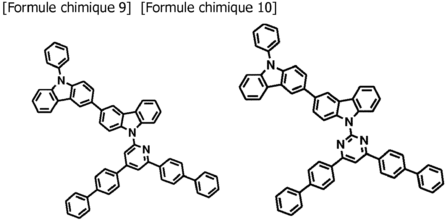
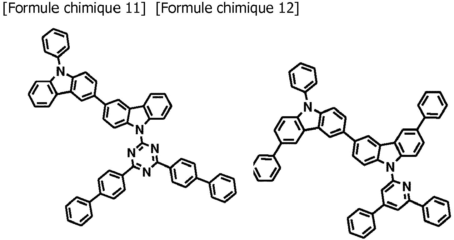
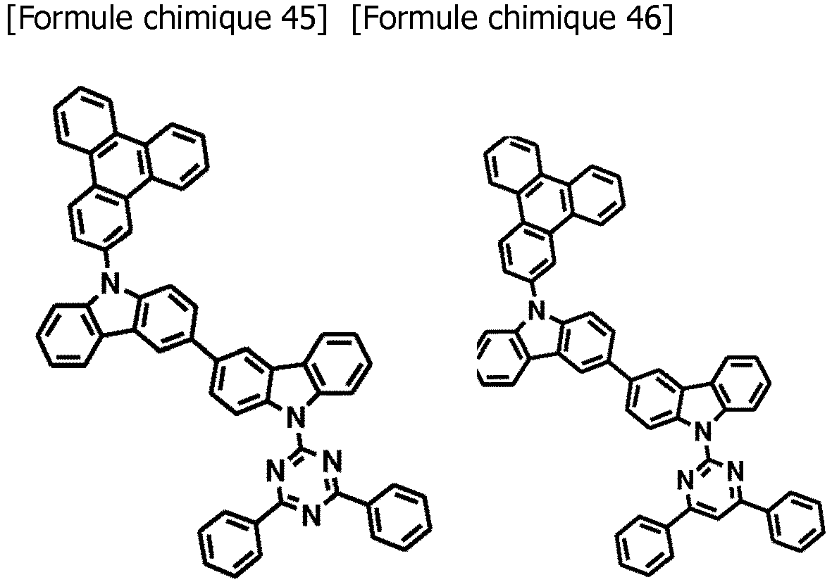
- the compound for an organic optoelectronic device according to the present invention is represented by the following Chemical Formulae 3, 6 to 48, 50 to 52 and 54.
- a compound for an organic optoelectronic device may be represented by one of the following Chemical Formulae A-2 to A-26, but is not limited thereto.
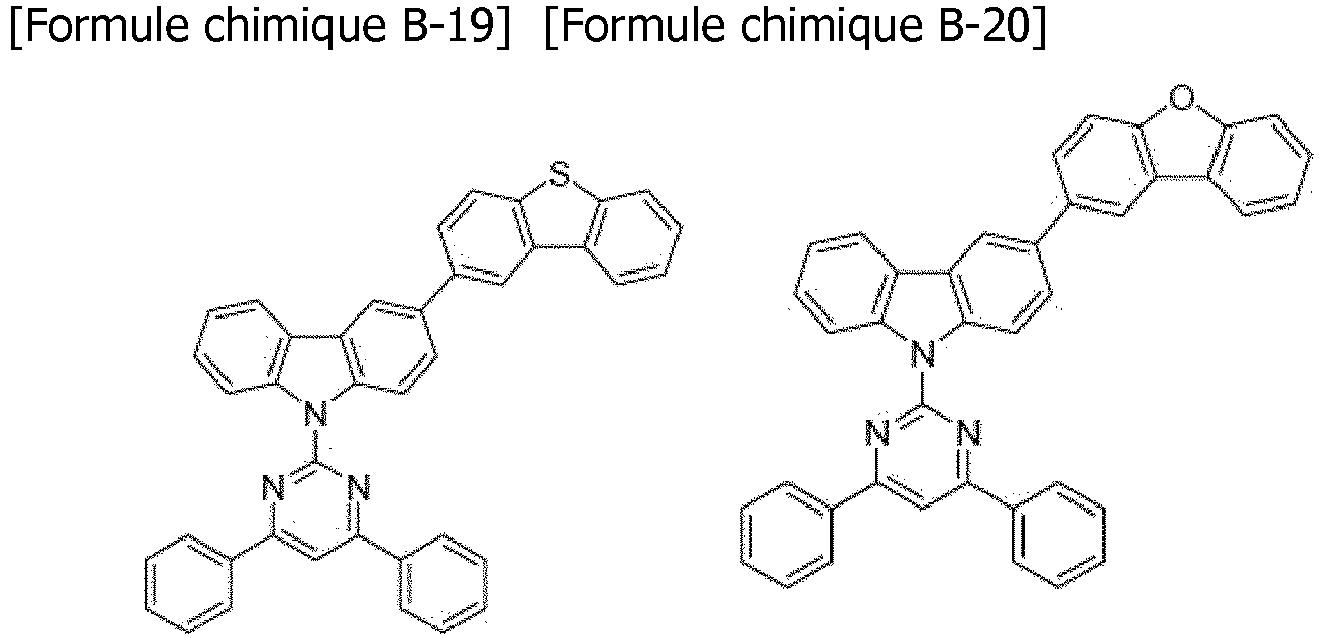
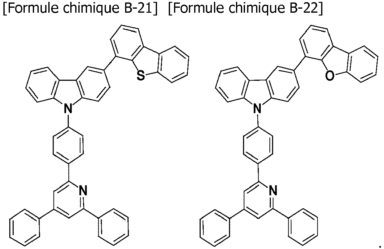
- the compound for an organic optoelectronic device according to the present invention is represented by one of the following Chemical Formulae B-3 to B-8, B-12 to B-17 and B-19 to B-22.
- the compound for an organic optoelectronic device according to the present invention is represented by one of the following Chemical Formulae C-3, C-6 to C-13 and C-15 to C-18.
- the compound for an organic optoelectronic device including the above compounds has a glass transition temperature of greater than or equal to 110°C and a thermal decomposition temperature of greater than or equal to 400°C, indicating improved thermal stability. Thereby, it is possible to produce an organic optoelectronic device having a high efficiency.
- the compound for an organic optoelectronic device including the above compounds may play a role for emitting light or injecting and/or transporting electrons, and also act as a light emitting host with an appropriate dopantln other words, the compound for an organic optoelectronic device may be used as a phosphorescent or fluorescent host material, a blue light emitting dopant material, or an electron transport material.
- the compound for an organic optoelectronic device is used for an organic thin layer, and it may improve the life-span characteristic, efficiency characteristic, electrochemical stability, and thermal stability of an organic photoelectric device and decrease the driving voltage.
- an organic optoelectronic device that includes the compound for an organic optoelectronic device.
- the organic optoelectronic device may include an organic photoelectric device, an organic light emitting diode, an organic solar cell, an organic transistor, an organic photo conductor drum, an organic memory device, and the like.
- the compound for an organic optoelectronic device according to one embodiment may be included in an electrode or an electrode buffer layer in the organic solar cell to improve the quantum efficiency, and it may be used as an electrode material for a gate, a source-drain electrode, or the like in the organic transistor.
- an organic light emitting diode includes an anode, a cathode, and at least one or more organic thin layer between the anode and the cathode, and at least one of the organic thin layer may include the compound for an organic optoelectronic device according to one embodiment.
- the organic thin layer that may include the compound for an organic optoelectronic device may include a layer selected from the group consisting of an emission layer, a hole transport layer (HTL), a hole injection layer (HIL), an electron transport layer (ETL), an electron injection layer (EIL), a hole blocking layer, and a combination thereof.
- the at least one layer includes the compound for an organic optoelectronic device according to one embodiment.
- the compound for an organic optoelectronic device according to one embodiment may be included in an electron transport layer (ETL) or an electron injection layer (EIL).
- the compound for an organic optoelectronic device may be included as a phosphorescent or fluorescent host, and particularly, as a fluorescent blue dopant material.
- FIGS. 1 to 5 are cross-sectional views showing organic light emitting diodes including the compound for an organic optoelectronic device according to one embodiment.
- organic light emitting diodes 100, 200, 300, 400, and 500 include at least one organic thin layer 105 interposed between an anode 120 and a cathode 110.
- the anode 120 includes an anode material laving a large work function to help hole injection into an organic thin layer.
- the anode material includes: a metal such as nickel, platinum, vanadium, chromium, copper, zinc, and gold, or alloys thereof; a metal oxide such as zinc oxide, indium oxide, indium tin oxide (ITO), and indium zinc oxide (IZO); a bonded metal and oxide such as ZnO:AI or SnO 2 :Sb; or a conductive polymer such as poly(3-methylthiophene), poly[3,4-(ethylene-1,2-dioxy)thiophene] (PEDT), polypyrrole, and polyaniline, but is not limited thereto. It is preferable to include a transparent electrode including indium tin oxide (ITO) as an anode.
- ITO indium tin oxide
- the cathode 110 includes a cathode material having a small work function to help electron injection into an organic thin layer.
- the cathode material includes: a metal such as magnesium, calcium, sodium, potassium, titanium, indium, yttrium, lithium, gadolinium, aluminum, silver, tin, and lead, or alloys thereof; or a multi-layered material such as LiF/Al, Liq/Al, LiO 2 /Al, LiF/Ca, LiF/Al, and BaF 2 /Ca, but is not limited thereto. It is preferable to include a metal electrode including aluminum as a cathode.
- the organic light emitting diode 100 includes an organic thin layer 105 including only an emission layer 130.
- a double-layered organic light emitting diode 200 includes an organic thin layer 105 including an emission layer 230 including an electron transport layer (ETL), and a hole transport layer (HTL) 140.
- the organic thin layer 105 includes a double layer of the emission layer 230 and hole transport layer (HTL) 140.
- the emission layer 130 also functions as an electron transport layer (ETL), and the hole transport layer (HTL) 140 layer has an excellent binding property with a transparent electrode such as ITO or an excellent hole transport capability.
- a three-layered organic light emitting diode 300 includes an organic thin layer 105 including an electron transport layer (ETL) 150, an emission layer 130, and a hole transport layer (HTL) 140.
- the emission layer 130 is independently installed, and layers having an excellent electron transport capability or an excellent hole transport capability are separately stacked.
- a four-layered organic light emitting diode 400 includes an organic thin layer 105 including an electron injection layer (EIL) 160, an emission layer 130, a hole transport layer (HTL) 140, and a hole injection layer (HIL) 170 for adherence with the cathode of ITO.
- EIL electron injection layer
- HTL hole transport layer
- HIL hole injection layer
- a five layered organic light emitting diode 500 includes an organic thin layer 105 including an electron transport layer (ETL) 150, an emission layer 130, a hole transport layer (HTL) 140, and a hole injection layer (HIL) 170, and further includes an electron injection layer (EIL) 160 to achieve a low voltage.
- ETL electron transport layer
- HTL hole transport layer
- HIL hole injection layer
- EIL electron injection layer
- the organic thin layer 105 including at least one selected from the group consisting of an electron transport layer (ETL) 150, an electron injection layer (EIL) 160, emission layers 130 and 230, a hole transport layer (HTL) 140, a hole injection layer (HIL) 170, and combinations thereof includes a compound for an organic optoelectronic device.
- the compound for an organic optoelectronic device may be used for an electron transport layer (ETL) 150 including the electron transport layer (ETL) 150 or electron injection layer (EIL) 160.
- ETL electron transport layer
- the material for the organic photoelectric device may be included as a phosphorescent or fluorescent host or a fluorescent blue dopant.
- the organic light emitting diode may be fabricated by: forming an anode on a substrate; forming an organic thin layer in accordance with a dry coating method such as evaporation, sputtering, plasma plating, and ion plating or a wet coating method such as spin coating, dipping, and flow coating; and providing a cathode thereon.
- a dry coating method such as evaporation, sputtering, plasma plating, and ion plating
- a wet coating method such as spin coating, dipping, and flow coating
- Another embodiment provides a display device including the organic light emitting diode according to the above embodiment.
- Example 1 Synthesis of Compound represented by Chemical Formula 4 (not forming part of the present invention)
- a compound represented by the above Chemical Formula 4 as a compound for an organic optoelectronic device was synthesized according to the following Reaction Scheme 1.
- Second Step Synthesis of Compound represented by Chemical Formula 4 3.5 g (8.55 mmol) of an intermediate product marked as the compound A, 2.74 g (10.26 mmol) of 2-chloro-4,6-diphenyl-pyrimidine, NaH, and dimethylformamide were put in a 100 mL round flask and then, agitated at room temperature under a nitrogen flow. Next, an organic solvent therein was distillated and removed under a reduced pressure and treated through a column chromatography, separating and obtaining a compound represented by Chemical Formula 4 3.823 g (yield: 70 %).
- a compound represented by the above Chemical Formula 5 as a compound for an organic optoelectronic device was synthesized according to the following Reaction Scheme 2.
- the compound represented by Chemical Formula 5 was element-analyzed. The result is as follows.
- a compound represented by the above Chemical Formula 14 as a compound for an organic optoelectronic device was synthesized according to the following Reaction Scheme 3.
- a compound represented by the above Chemical Formula A-2 as an exemplary compound for an organic optoelectronic device was synthesized according to the following Reaction Scheme 4.
- a compound represented by the above Chemical Formula A-10 as an exemplary compound for an organic optoelectronic device was synthesized according to the following Reaction Scheme 5.
- a compound represented by the above Chemical Formula A-12 as an exemplary compound for an organic optoelectronic device was synthesized according to the following Reaction Scheme 3.
- a compound represented by the above Chemical Formula B-8 as an exemplary compound for an organic optoelectronic was synthesized according to the following Reaction Scheme 8.
- a compound represented by the above Chemical Formula 3 as an exemplary compound for an organic optoelectronic device was synthesized according to the following Reaction Scheme 10.
- a compound represented by the above Chemical Formula 54 as an exemplary compound for an organic optoelectronic device was synthesized according to the following Reaction Scheme 11.
- Example 13 (not forming part of the present invention)
- An organic light emitting diode was fabricated by using the compound according to Example 1 and lr(PPy) 3 as a dopant.
- 1000 A-thick ITO was used as a positive electrode
- 1000 A-thick aluminum (Al) was used as a cathode.
- a method of manufacturing the organic light emitting diode included cutting an ITO glass substrate having sheet resistance of 15 ⁇ /cm 2 into a size of 50 mm ⁇ 50 mm ⁇ 0.7 mm and ultrasonic wave-cleaning it in acetone, isopropylalcohol, and pure water for 15 minutes respectively and then, UV-ozone cleaning it for 30 minutes.
- a 800 A-thick hole transport layer (HTL) was formed by depositing N,N'-di(1-naphthyl)-N,N'-diphenylbenzidine (NPB) (70 nm) and 4,4',4"-tri(N-carbazolyl)triphenylamine (TCTA) (10 nm) under conditions of a vacuum degree of 650 ⁇ 10 -7 Pa and a deposition rate of 0.1 to 0.3 nm/s.
- NPB N,N'-di(1-naphthyl)-N,N'-diphenylbenzidine
- TCTA 4,4',4"-tri(N-carbazolyl)triphenylamine
- a 300 A-thick emission layer was formed thereon using the compound according to Example 2 under the same vacuum deposit conditions, and lr(PPy) 3 as a phosphorescence dopant was simultaneously deposited.
- the deposition rate of the phosphorescence dopant was adjusted to include 7 wt% of the phosphorescence dopant based on 100 wt% of the emission layer.
- BAIq bis(8-hydroxy-2-methylquinolinolato)-aluminumbiphenoxide
- ETL electron transport layer
- the organic photoelectric device had a structure of ITO/ NPB (70 nm)/ TCTA (10 nm)/ EML (the compound of Example 1 (93 wt%) + lr(PPy) 3 (7 wt%), 30 nm)/ Balq (5 nm)/ Alq 3 (20 nm)/ LiF (1 nm) / Al (100 nm).
- Example 14 (not forming part of the present invention)
- An organic light emitting diode was fabricated according to the same method as Example 13 except for using the compound according to Example 2 as a host for an emission layer instead of the compound according to Example 1.
- Example 15 (not forming part of the present invention)
- An organic light emitting diode was fabricated according to the same method as Example 13 except for using the compound according to Example 4 as a host for an emission layer instead of the compound according to Example 1.
- Example 16 (not forming part of the present invention)
- An organic light emitting diode was fabricated according to the same method as Example 13 except for using the compound according to Example 6 as a host for an emission layer instead of the compound according to Example 1.
- An organic light emitting diode was fabricated according to the same method as Example 13 except for using the compound according to Example 7 as a host for an emission layer instead of the compound according to Example 1.
- An organic light emitting diode was fabricated according to the same method as Example 13 except for using the compound according to Example 10 as a host for an emission layer instead of the compound according to Example 1.
- An organic light emitting diode was fabricated according to the same method as Example 13 except for using the compound according to Example 12 as a host for an emission layer instead of the compound according to Example 1.
- An organic light emitting diode was fabricated according to the same method as Example 13 except for using the compound according to Example 12 as a host for an emission layer instead of the compound according to Example 1.
- An organic light emitting diode was fabricated according to the same method as Example 13 except for using 4,4-N,N-dicarbazolebiphenyl (CBP) as a host for an emission layer instead of the compound according to Example 2.
- CBP 4,4-N,N-dicarbazolebiphenyl
- the fabricated organic light emitting diodes were measured for current value flowing in the unit device while increasing the voltage from 0V to 10V using a current-voltage meter (Keithley 2400), and the measured current value was divided by area to provide the result.
- the fabricated organic light emitting diodes were measured for luminance while increasing the voltage form 0V to 10V using a luminance meter (Minolta Cs-1000A).
- a device fabricated using a material according to the present invention had excellent driving voltage and efficiency compared with one fabricated using CBP, a reference material in terms of luminous efficiency.
- life-span was evaluated by measuring time until 3% luminous efficiency decreased.
- the device fabricated using CBP had a very short life-span of less than one hour, while the device fabricated using the compound of the present invention had a life-span ranging from 10 hours to 60 hours at most.
- the device according to Comparative Example 2 had luminous efficiency ranging from 30 to 35 cd/A, which was remarkably lower than the ones according to Examples 13 to 20.
- the compound according to the present invention may be well applied to an organic light emitting diode.
Landscapes
- Chemical & Material Sciences (AREA)
- Organic Chemistry (AREA)
- Engineering & Computer Science (AREA)
- Materials Engineering (AREA)
- Physics & Mathematics (AREA)
- Spectroscopy & Molecular Physics (AREA)
- Optics & Photonics (AREA)
- Electroluminescent Light Sources (AREA)
- Plural Heterocyclic Compounds (AREA)
- Organic Low-Molecular-Weight Compounds And Preparation Thereof (AREA)
Claims (7)
- Composé destiné à un dispositif optoélectronique organique, en particulier, destiné à un dispositif photoélectrique organique, une diode émettant une lumière organique, une cellule solaire organique, un transistor organique, un tambour de conducteur photo organique, ou un dispositif de mémoire organique, représenté par une des formules chimiques suivantes 3, 6 à 48, 50 à 52, 54, C-3, C-6 à C-13 et C-15 à C-18 :






- Composé destiné à un dispositif optoélectronique organique, en particulier, destiné à un dispositif photoélectrique organique, une diode émettant une lumière organique, une cellule solaire organique, un transistor organique, un tambour de conducteur photo organique, ou un dispositif de mémoire organique, où le composé destiné à un dispositif optoélectronique est représenté par la formule chimique suivante B :
 X1 est choisi dans le groupe constitué de -O- et -S-,les groupes R1 à R6 sont identiques ou différents et sont indépendamment choisis dans le groupe constitué d'atomes d'hydrogène, de deutérium, d'un groupe alkyle en C1 à C20 substitué ou non substitué, d'un groupe aryle en C6 à C30 substitué ou non substitué, et d'un groupe hétéroaryle en C2 à C30 substitué ou non substitué,Ar est un groupe hétéroaryle en C2 à C30 substitué ou non substitué ayant des propriétés électroniques, où le groupe hétéroaryle en C2 à C30 substitué ou non substitué ayant des propriétés électroniques est choisi parmi un groupe pyridinyle substitué ou non substitué, un groupe pyrimidyle substitué ou non substitué et un groupe triazinyle substitué ou non substitué,L est choisi dans le groupe constitué d'une liaison simple, d'un groupe alcénylène en C2 à C10 substitué ou non substitué, d'un groupe alcynylène en C2 à C10 substitué ou non substitué, d'un groupe arylène en C6 à C30 substitué ou non substitué et d'un groupe hétéroarylène en C2 à C30 substitué ou non substitué, et n est un nombre entier allant de 0 à 2.
 - Composé destiné à un dispositif optoélectronique organique selon la revendication 2, où le composé destiné à un dispositif optoélectronique est représenté par les formules chimiques suivantes B-1 ou B-2 :


 X1 est choisi dans le groupe constitué de -O- et -S-,les groupes R1 à R6 sont identiques ou différents et sont indépendamment choisis dans le groupe constitué d'atomes d'hydrogène, de deutérium, d'un groupe alkyle en C1 à C20 substitué ou non substitué, d'un groupe aryle en C6 à C30 substitué ou non substitué, et d'un groupe hétéroaryle en C2 à C30 substitué ou non substitué,Ar est un groupe hétéroaryle en C2 à C30 substitué ou non substitué ayant des propriétés électroniques, où le groupe hétéroaryle en C2 à C30 substitué ou non substitué ayant des propriétés électroniques est choisi parmi un groupe pyridinyle substitué ou non substitué, un groupe pyrimidyle substitué ou non substitué et un groupe triazinyle substitué ou non substitué,L est une liaison simple, un groupe alcénylène en C2 à C10 substitué ou non substitué, un groupe alcynylène en C2 à C10 substitué ou non substitué, un groupe arylène en C6 à C30 substitué ou non substitué et un groupe hétéroarylène en C2 à C30 substitué ou non substitué, etn est un nombre entier allant de 0 à 2.
 - Composé destiné à un dispositif optoélectronique organique selon la revendication 2 ou la revendication 3, où le composé destiné à un dispositif optoélectronique organique est représenté par une des formules chimiques suivantes B-3 à B-8, B-12 à B-17 et B-19 à B-22.


- Diode émettant une lumière organique, comprenant une diode émettant de la lumière organique incluant une anode, une cathode et au moins une ou plusieurs couches fines organiques entre l'anode et la cathode, où l'au moins une couche fine organique, particulièrement l'une parmi une couche d'émission, une couche de transport de trous (HTL), une couche d'injection de trous (HIL), une couche de transport d'électrons (ETL), une couche d'injection d'électrons (EIL), une couche de blocage de trous, et une combinaison de celles-ci, comprend le composé destiné à un dispositif optoélectronique selon l'une quelconque des revendications 1 à 4.
- Diode émettant une lumière organique selon la revendication 5, dans laquelle le composé destiné à un dispositif optoélectronique est utilisé en tant que matériau hôte phosphorescent ou fluorescent dans une couche d'émission ou en tant que matériau dopant bleu fluorescent dans une couche d'émission.
- Dispositif d'affichage comprenant la diode émettant une lumière organique selon la revendication 5 ou la revendication 6.
Priority Applications (2)
| Application Number | Priority Date | Filing Date | Title |
|---|---|---|---|
| EP19155683.6A EP3514846B1 (fr) | 2010-05-03 | 2011-04-29 | Composé pour dispositif opto-électronique organique, diode électroluminescente organique l'incluant et dispositif d'affichage incluant la diode électroluminescente organique |
| EP19155679.4A EP3509121B1 (fr) | 2010-05-03 | 2011-04-29 | Composé pour dispositif opto-électronique organique, diode électroluminescente organique l'incluant et afficheur incluant la diode électroluminescente organique |
Applications Claiming Priority (3)
| Application Number | Priority Date | Filing Date | Title |
|---|---|---|---|
| KR20100041466 | 2010-05-03 | ||
| KR1020100106077A KR20110122051A (ko) | 2010-05-03 | 2010-10-28 | 유기광전소자용 화합물 및 이를 포함하는 유기광전소자 |
| PCT/KR2011/003235 WO2011139055A2 (fr) | 2010-05-03 | 2011-04-29 | Composé pour dispositif optoélectronique organique, diode électroluminescente organique comprenant ledit composé, et dispositif d'affichage comprenant une diode électroluminescente organique |
Related Child Applications (4)
| Application Number | Title | Priority Date | Filing Date |
|---|---|---|---|
| EP19155683.6A Division EP3514846B1 (fr) | 2010-05-03 | 2011-04-29 | Composé pour dispositif opto-électronique organique, diode électroluminescente organique l'incluant et dispositif d'affichage incluant la diode électroluminescente organique |
| EP19155683.6A Division-Into EP3514846B1 (fr) | 2010-05-03 | 2011-04-29 | Composé pour dispositif opto-électronique organique, diode électroluminescente organique l'incluant et dispositif d'affichage incluant la diode électroluminescente organique |
| EP19155679.4A Division EP3509121B1 (fr) | 2010-05-03 | 2011-04-29 | Composé pour dispositif opto-électronique organique, diode électroluminescente organique l'incluant et afficheur incluant la diode électroluminescente organique |
| EP19155679.4A Division-Into EP3509121B1 (fr) | 2010-05-03 | 2011-04-29 | Composé pour dispositif opto-électronique organique, diode électroluminescente organique l'incluant et afficheur incluant la diode électroluminescente organique |
Publications (3)
| Publication Number | Publication Date |
|---|---|
| EP2568030A2 EP2568030A2 (fr) | 2013-03-13 |
| EP2568030A4 EP2568030A4 (fr) | 2014-11-26 |
| EP2568030B1 true EP2568030B1 (fr) | 2019-12-25 |
Family
ID=45392753
Family Applications (3)
| Application Number | Title | Priority Date | Filing Date |
|---|---|---|---|
| EP19155683.6A Active EP3514846B1 (fr) | 2010-05-03 | 2011-04-29 | Composé pour dispositif opto-électronique organique, diode électroluminescente organique l'incluant et dispositif d'affichage incluant la diode électroluminescente organique |
| EP11777536.1A Active EP2568030B1 (fr) | 2010-05-03 | 2011-04-29 | Composé pour dispositif optoélectronique organique, diode électroluminescente organique comprenant ledit composé, et dispositif d'affichage comprenant une diode électroluminescente organique |
| EP19155679.4A Active EP3509121B1 (fr) | 2010-05-03 | 2011-04-29 | Composé pour dispositif opto-électronique organique, diode électroluminescente organique l'incluant et afficheur incluant la diode électroluminescente organique |
Family Applications Before (1)
| Application Number | Title | Priority Date | Filing Date |
|---|---|---|---|
| EP19155683.6A Active EP3514846B1 (fr) | 2010-05-03 | 2011-04-29 | Composé pour dispositif opto-électronique organique, diode électroluminescente organique l'incluant et dispositif d'affichage incluant la diode électroluminescente organique |
Family Applications After (1)
| Application Number | Title | Priority Date | Filing Date |
|---|---|---|---|
| EP19155679.4A Active EP3509121B1 (fr) | 2010-05-03 | 2011-04-29 | Composé pour dispositif opto-électronique organique, diode électroluminescente organique l'incluant et afficheur incluant la diode électroluminescente organique |
Country Status (6)
| Country | Link |
|---|---|
| US (1) | US9543530B2 (fr) |
| EP (3) | EP3514846B1 (fr) |
| JP (1) | JP5938397B2 (fr) |
| KR (1) | KR20110122051A (fr) |
| CN (1) | CN102971395B (fr) |
| WO (1) | WO2011139055A2 (fr) |
Families Citing this family (119)
| Publication number | Priority date | Publication date | Assignee | Title |
|---|---|---|---|---|
| EP2445905A1 (fr) * | 2009-06-24 | 2012-05-02 | Georgia Tech Research Corporation | Hôtes ambipolaires polymérisables pour émetteurs invités phosphorescents |
| JP6049998B2 (ja) | 2009-08-28 | 2016-12-21 | 保土谷化学工業株式会社 | カルバゾール環構造を有する化合物および有機エレクトロルミネッセンス素子 |
| KR20110122051A (ko) | 2010-05-03 | 2011-11-09 | 제일모직주식회사 | 유기광전소자용 화합물 및 이를 포함하는 유기광전소자 |
| WO2011162162A1 (fr) * | 2010-06-24 | 2011-12-29 | 東レ株式会社 | Matériau de dispositif électroluminescent et dispositif électroluminescent |
| KR102004629B1 (ko) * | 2010-08-20 | 2019-07-26 | 유니버셜 디스플레이 코포레이션 | Oled를 위한 바이카르바졸 화합물 |
| JP5623996B2 (ja) * | 2010-09-21 | 2014-11-12 | 株式会社半導体エネルギー研究所 | カルバゾール誘導体 |
| JP5856266B2 (ja) * | 2010-09-21 | 2016-02-09 | 株式会社半導体エネルギー研究所 | 有機半導体素子 |
| US9133173B2 (en) * | 2010-10-15 | 2015-09-15 | Semiconductor Energy Laboratory Co., Ltd. | Carbazole compound, material for light-emitting element, organic semiconductor material, light-emitting element |
| WO2012069121A1 (fr) * | 2010-11-24 | 2012-05-31 | Merck Patent Gmbh | Matériaux pour dispositifs d'électroluminescence organiques |
| EP2662368A4 (fr) | 2010-12-20 | 2014-06-25 | Idemitsu Kosan Co | Dérivé d'hétérocycle aromatique et élément électroluminescent organique utilisant celui-ci |
| KR101478000B1 (ko) * | 2010-12-21 | 2015-01-05 | 롬엔드하스전자재료코리아유한회사 | 신규한 유기 발광 화합물 및 이를 채용하고 있는 유기 전계 발광 소자 |
| JP5870045B2 (ja) | 2011-02-07 | 2016-02-24 | 出光興産株式会社 | ビスカルバゾール誘導体及びそれを用いた有機エレクトロルミネッセンス素子 |
| US10147888B2 (en) * | 2011-02-07 | 2018-12-04 | Idemitsu Kosan Co., Ltd. | Biscarbazole derivative and organic electroluminescent element using same |
| EP2688120B1 (fr) | 2011-03-14 | 2017-08-23 | Toray Industries, Inc. | Matériau d'élément d'émission de lumière et élément d'émission de lumière |
| WO2012128298A1 (fr) * | 2011-03-24 | 2012-09-27 | 出光興産株式会社 | Dérivé de bis-carbazole et élément électroluminescent organique l'utilisant |
| KR20120109744A (ko) * | 2011-03-25 | 2012-10-09 | 롬엔드하스전자재료코리아유한회사 | 신규한 유기 전자재료용 화합물 및 이를 포함하는 유기 전계 발광 소자 |
| JP6197265B2 (ja) * | 2011-03-28 | 2017-09-20 | 東レ株式会社 | 発光素子材料および発光素子 |
| BR112013027966A2 (pt) | 2011-05-12 | 2017-01-17 | Toray Industries | material do dispositivo emissor de luz e dispositivo emissor de luz |
| JP5946692B2 (ja) * | 2011-05-13 | 2016-07-06 | 株式会社半導体エネルギー研究所 | カルバゾール化合物、有機半導体素子、発光素子、発光装置、照明装置、表示装置、電子機器 |
| KR101443756B1 (ko) * | 2011-05-26 | 2014-09-23 | 제일모직 주식회사 | 유기광전자소자용 화합물, 이를 포함하는 유기발광소자 및 상기 유기발광소자를 포함하는 표시장치 |
| KR101354638B1 (ko) | 2011-06-20 | 2014-01-22 | 제일모직주식회사 | 유기광전자소자용 재료, 이를 포함하는 유기발광소자 및 상기 유기발광소자를 포함하는 표시장치 |
| KR20130011955A (ko) * | 2011-07-21 | 2013-01-30 | 롬엔드하스전자재료코리아유한회사 | 신규한 유기 발광 화합물 및 이를 채용하고 있는 유기 전계 발광 소자 |
| WO2013012298A1 (fr) * | 2011-07-21 | 2013-01-24 | Rohm And Haas Electronic Materials Korea Ltd. | Composés 9h-carbazole et dispositifs électroluminescents comprenant ces derniers |
| JP6034005B2 (ja) * | 2011-08-03 | 2016-11-30 | 出光興産株式会社 | ビスカルバゾール誘導体およびこれを用いた有機エレクトロルミネッセンス素子 |
| KR20130020398A (ko) * | 2011-08-19 | 2013-02-27 | 제일모직주식회사 | 유기광전자소자용 화합물, 이를 포함하는 유기발광소자 및 상기 유기발광소자를 포함하는 표시장치 |
| KR102025031B1 (ko) | 2011-11-22 | 2019-11-14 | 이데미쓰 고산 가부시키가이샤 | 방향족 복소고리 유도체, 유기 일렉트로루미네선스 소자용 재료 및 유기 일렉트로루미네선스 소자 |
| JP2013116975A (ja) * | 2011-12-02 | 2013-06-13 | Kyushu Univ | 遅延蛍光材料、有機発光素子および化合物 |
| EP2787549A4 (fr) * | 2011-12-02 | 2015-09-23 | Univ Kyushu Nat Univ Corp | Dispositif organique émettant de la lumière et matière à fluorescence retardée et composant utilisé dans celui-ci |
| CN103959503B (zh) * | 2011-12-05 | 2016-08-24 | 出光兴产株式会社 | 有机电致发光元件用材料以及有机电致发光元件 |
| KR20130062583A (ko) * | 2011-12-05 | 2013-06-13 | 롬엔드하스전자재료코리아유한회사 | 신규한 유기 발광 화합물 및 이를 채용하고 있는 유기 전계 발광 소자 |
| WO2013105206A1 (fr) | 2012-01-10 | 2013-07-18 | 出光興産株式会社 | Matériau pour élément électroluminescent organique, et élément comprenant ce matériau |
| JP5397568B1 (ja) * | 2012-02-15 | 2014-01-22 | 東レ株式会社 | 発光素子材料および発光素子 |
| JP6361138B2 (ja) * | 2012-03-05 | 2018-07-25 | 東レ株式会社 | 発光素子 |
| JP2015155378A (ja) * | 2012-04-18 | 2015-08-27 | 保土谷化学工業株式会社 | トリフェニレン環構造を有する化合物および有機エレクトロルミネッセンス素子 |
| KR20130121479A (ko) * | 2012-04-27 | 2013-11-06 | 롬엔드하스전자재료코리아유한회사 | 신규한 유기 전계 발광 화합물 및 이를 포함하는 유기 전계 발광 소자 |
| CN104507927A (zh) * | 2012-06-18 | 2015-04-08 | 东曹株式会社 | 环状吖嗪化合物、其制造方法、及含有其的有机电致发光元件 |
| TWI564297B (zh) * | 2012-06-18 | 2017-01-01 | Tosoh Corp | ring A compound, a method for producing the same, and an organic electroluminescent device containing the same |
| KR101344787B1 (ko) | 2012-07-04 | 2013-12-26 | 제일모직주식회사 | 유기광전자소자용 화합물, 이를 포함하는 유기발광소자 및 상기 유기발광소자를 포함하는 표시장치 |
| JP2015524610A (ja) * | 2012-07-04 | 2015-08-24 | サムスン エスディアイ カンパニー,リミテッド | 有機発光素子用組成物、これを含む有機発光層および有機発光素子 |
| CN104488105B (zh) | 2012-07-25 | 2017-03-22 | 东丽株式会社 | 发光元件材料和发光元件 |
| JP5966736B2 (ja) * | 2012-07-31 | 2016-08-10 | 東ソー株式会社 | カルバゾール化合物、その製造法、及びその用途 |
| TWI650399B (zh) | 2012-08-03 | 2019-02-11 | 日商半導體能源研究所股份有限公司 | 發光元件 |
| KR101497138B1 (ko) * | 2012-08-21 | 2015-02-27 | 제일모직 주식회사 | 유기광전자소자 및 이를 포함하는 표시장치 |
| JP2014072417A (ja) * | 2012-09-28 | 2014-04-21 | Idemitsu Kosan Co Ltd | 有機エレクトロルミネッセンス素子用材料及び有機エレクトロルミネッセンス素子 |
| US10297761B2 (en) | 2012-12-10 | 2019-05-21 | Idemitsu Kosan Co., Ltd. | Organic electroluminescent element |
| KR102055684B1 (ko) | 2012-12-27 | 2020-01-23 | 삼성디스플레이 주식회사 | 유기 발광 소자 |
| KR102190183B1 (ko) * | 2012-12-28 | 2020-12-11 | 이데미쓰 고산 가부시키가이샤 | 유기 일렉트로 루미네선스 소자 |
| KR101820865B1 (ko) | 2013-01-17 | 2018-01-22 | 삼성전자주식회사 | 유기광전자소자용 재료, 이를 포함하는 유기발광소자 및 상기 유기발광소자를 포함하는 표시장치 |
| KR102065656B1 (ko) * | 2013-02-19 | 2020-01-13 | 덕산네오룩스 주식회사 | 유기전기 소자용 화합물, 이를 이용한 유기전기소자 및 그 전자 장치 |
| JP2016122672A (ja) * | 2013-03-18 | 2016-07-07 | 出光興産株式会社 | 発光装置 |
| US10043982B2 (en) | 2013-04-26 | 2018-08-07 | Semiconductor Energy Laboratory Co., Ltd. | Light-emitting element, light-emitting device, display device, electronic device, and lighting device |
| WO2014185535A1 (fr) * | 2013-05-16 | 2014-11-20 | ダイキン工業株式会社 | Dérivé de fullerène et matériau de semi-conducteur de type n |
| KR102162795B1 (ko) | 2013-06-07 | 2020-10-08 | 삼성디스플레이 주식회사 | 헤테로고리 화합물 및 이를 포함한 유기 발광 소자 |
| KR102117609B1 (ko) | 2013-06-26 | 2020-06-02 | 삼성디스플레이 주식회사 | 헤테로고리 화합물 및 이를 포함한 유기 발광 소자 |
| KR101566434B1 (ko) * | 2013-07-15 | 2015-11-06 | 삼성디스플레이 주식회사 | 유기 발광 장치 |
| KR101547065B1 (ko) | 2013-07-29 | 2015-08-25 | 주식회사 엘지화학 | 헤테로 고리 화합물 및 이를 포함하는 유기 발광 소자 |
| KR102116496B1 (ko) | 2013-08-26 | 2020-05-29 | 삼성디스플레이 주식회사 | 유기 발광 소자 |
| KR101812581B1 (ko) | 2013-10-11 | 2017-12-27 | 제일모직 주식회사 | 유기광전자소자용 유기합화물, 유기 광전자 소자 및 표시 장치 |
| KR102140006B1 (ko) * | 2013-10-11 | 2020-07-31 | 에스에프씨 주식회사 | 유기발광 화합물 및 이를 포함하는 유기전계발광소자 |
| KR20150071624A (ko) * | 2013-12-18 | 2015-06-26 | 롬엔드하스전자재료코리아유한회사 | 유기 전계 발광 화합물 및 이를 포함하는 유기 전계 발광 소자 |
| KR101846436B1 (ko) * | 2014-01-29 | 2018-04-06 | 제일모직 주식회사 | 전자수송보조층용 조성물, 전자수송보조층을 포함하는 유기 광전자 소자 및 표시 장치 |
| WO2015115744A1 (fr) * | 2014-01-29 | 2015-08-06 | 삼성에스디아이 주식회사 | Composition pour couche auxiliaire de transport d'électrons, dispositif optoélectrique organique contenant la couche auxiliaire de transport d'électrons, et dispositif d'affichage |
| KR20150099192A (ko) * | 2014-02-21 | 2015-08-31 | 삼성에스디아이 주식회사 | 유기 광전자 소자 및 표시 장치 |
| WO2015126081A1 (fr) * | 2014-02-21 | 2015-08-27 | 삼성에스디아이 주식회사 | Dispositif optoélectrique organique et appareil d'affichage |
| KR20150108330A (ko) * | 2014-03-17 | 2015-09-25 | 롬엔드하스전자재료코리아유한회사 | 전자 버퍼 재료 및 이를 포함하는 유기 전계 발광 소자 |
| KR101754715B1 (ko) | 2014-04-08 | 2017-07-10 | 롬엔드하스전자재료코리아유한회사 | 복수종의 호스트 재료와 이를 포함하는 유기 전계 발광 소자 |
| KR101773363B1 (ko) | 2014-04-09 | 2017-08-31 | 제일모직 주식회사 | 유기 화합물, 조성물, 유기 광전자 소자 및 표시 장치 |
| KR102255197B1 (ko) | 2014-05-02 | 2021-05-25 | 삼성디스플레이 주식회사 | 유기 발광 소자 |
| US9589727B2 (en) * | 2014-05-12 | 2017-03-07 | Capacitor Sciences Incorporated | Capacitor and method of production thereof |
| CN110085424B (zh) | 2014-05-12 | 2021-05-18 | 柯帕瑟特科学有限责任公司 | 能量储存器件及其制造方法 |
| US10319523B2 (en) | 2014-05-12 | 2019-06-11 | Capacitor Sciences Incorporated | Yanli dielectric materials and capacitor thereof |
| US20170301477A1 (en) | 2016-04-04 | 2017-10-19 | Capacitor Sciences Incorporated | Electro-polarizable compound and capacitor |
| US10347423B2 (en) | 2014-05-12 | 2019-07-09 | Capacitor Sciences Incorporated | Solid multilayer structure as semiproduct for meta-capacitor |
| US10340082B2 (en) | 2015-05-12 | 2019-07-02 | Capacitor Sciences Incorporated | Capacitor and method of production thereof |
| KR101631507B1 (ko) * | 2014-07-01 | 2016-06-20 | 원광대학교산학협력단 | 유기전계발광소자용 정공수송물질 및 이를 이용한 유기전계발광소자 |
| FR3024144B1 (fr) * | 2014-07-28 | 2017-05-19 | Univ De Tours Francois-Rabelais | Nouveaux synthons pour l'elaboration de semi-conducteurs organiques |
| KR101825542B1 (ko) * | 2014-08-26 | 2018-02-05 | 삼성에스디아이 주식회사 | 유기 광전자 소자 및 표시장치 |
| KR102304720B1 (ko) * | 2014-09-19 | 2021-09-27 | 삼성디스플레이 주식회사 | 유기 발광 소자 |
| US20160104855A1 (en) | 2014-10-10 | 2016-04-14 | Semiconductor Energy Laboratory Co., Ltd. | Light-Emitting Element, Display Device, Electronic Device, and Lighting Device |
| KR101825541B1 (ko) * | 2014-10-15 | 2018-02-05 | 삼성에스디아이 주식회사 | 유기 광전자 소자 및 표시 장치 |
| KR101818581B1 (ko) * | 2014-10-31 | 2018-01-15 | 삼성에스디아이 주식회사 | 유기 광전자 소자 및 표시 장치 |
| MX2017005427A (es) | 2014-11-04 | 2017-06-21 | Capacitor Sciences Inc | Dispositivos de almacenamiento de energia y metodos de produccion de los mismos. |
| KR102384649B1 (ko) | 2014-11-10 | 2022-04-11 | 삼성디스플레이 주식회사 | 유기 발광 소자 |
| KR102285388B1 (ko) * | 2014-11-13 | 2021-08-04 | 삼성디스플레이 주식회사 | 유기 발광 소자 |
| KR102385230B1 (ko) | 2014-11-19 | 2022-04-12 | 삼성디스플레이 주식회사 | 유기 발광 소자 |
| KR102363260B1 (ko) * | 2014-12-19 | 2022-02-16 | 삼성디스플레이 주식회사 | 유기 발광 소자 |
| KR101706752B1 (ko) * | 2015-02-17 | 2017-02-27 | 서울대학교산학협력단 | 호스트, 인광 도펀트 및 형광 도펀트를 포함하는 유기발광소자 |
| KR20170118764A (ko) | 2015-02-26 | 2017-10-25 | 캐패시터 사이언시스 인코포레이티드 | 자기-회복 커패시터 및 이들의 생산 방법 |
| TWI704706B (zh) | 2015-03-09 | 2020-09-11 | 日商半導體能源研究所股份有限公司 | 發光元件、顯示裝置、電子裝置及照明設置 |
| US9932358B2 (en) | 2015-05-21 | 2018-04-03 | Capacitor Science Incorporated | Energy storage molecular material, crystal dielectric layer and capacitor |
| US9941051B2 (en) | 2015-06-26 | 2018-04-10 | Capactor Sciences Incorporated | Coiled capacitor |
| US10651392B2 (en) | 2015-09-30 | 2020-05-12 | Samsung Electronics Co., Ltd. | Organic light-emitting device |
| US10026553B2 (en) | 2015-10-21 | 2018-07-17 | Capacitor Sciences Incorporated | Organic compound, crystal dielectric layer and capacitor |
| KR102507371B1 (ko) * | 2015-12-03 | 2023-03-08 | 솔루스첨단소재 주식회사 | 유기 발광 화합물 및 이를 이용한 유기 전계 발광 소자 |
| JP6788314B2 (ja) * | 2016-01-06 | 2020-11-25 | コニカミノルタ株式会社 | 有機エレクトロルミネッセンス素子、有機エレクトロルミネッセンス素子の製造方法、表示装置及び照明装置 |
| US10305295B2 (en) | 2016-02-12 | 2019-05-28 | Capacitor Sciences Incorporated | Energy storage cell, capacitive energy storage module, and capacitive energy storage system |
| US10636575B2 (en) | 2016-02-12 | 2020-04-28 | Capacitor Sciences Incorporated | Furuta and para-Furuta polymer formulations and capacitors |
| US10153087B2 (en) | 2016-04-04 | 2018-12-11 | Capacitor Sciences Incorporated | Electro-polarizable compound and capacitor |
| US10566138B2 (en) | 2016-04-04 | 2020-02-18 | Capacitor Sciences Incorporated | Hein electro-polarizable compound and capacitor thereof |
| US9978517B2 (en) | 2016-04-04 | 2018-05-22 | Capacitor Sciences Incorporated | Electro-polarizable compound and capacitor |
| CN109071501B (zh) * | 2016-05-04 | 2021-07-09 | 辛诺拉有限公司 | 特别用于有机光电器件的有机分子 |
| KR102005867B1 (ko) * | 2016-06-17 | 2019-07-31 | 삼성에스디아이 주식회사 | 유기 광전자 소자용 조성물, 유기 광전자 소자 및 표시 장치 |
| US10137876B2 (en) | 2016-09-30 | 2018-11-27 | Advics Co., Ltd. | Braking control device for vehicle |
| US10395841B2 (en) | 2016-12-02 | 2019-08-27 | Capacitor Sciences Incorporated | Multilayered electrode and film energy storage device |
| WO2019171197A1 (fr) | 2018-03-07 | 2019-09-12 | 株式会社半導体エネルギー研究所 | Élément électroluminescent, dispositif d'affichage, dispositif électronique, composé organique et dispositif d'éclairage |
| KR102206482B1 (ko) | 2018-04-24 | 2021-01-22 | 주식회사 엘지화학 | 신규한 헤테로 고리 화합물 및 이를 이용한 유기발광 소자 |
| CN108774239B (zh) * | 2018-06-14 | 2021-04-20 | 宁波卢米蓝新材料有限公司 | 一种稠环化合物及其制备方法和用途 |
| US12545834B2 (en) | 2018-07-11 | 2026-02-10 | Semiconductor Energy Laboratory Co., Ltd. | Light-emitting device, display device, electronic device, organic compound, and lighting device |
| US12501828B2 (en) * | 2018-12-28 | 2025-12-16 | Samsung Electronics Co., Ltd. | Organic light-emitting device and apparatus including the same |
| JP7341172B2 (ja) | 2019-02-06 | 2023-09-08 | 株式会社半導体エネルギー研究所 | 発光デバイス、電子機器及び照明装置 |
| WO2020217129A1 (fr) | 2019-04-25 | 2020-10-29 | 株式会社半導体エネルギー研究所 | Dispositif électroluminescent, appareil électroluminescent, dispositif électronique et dispositif d'éclairage |
| WO2021044262A1 (fr) | 2019-09-06 | 2021-03-11 | 株式会社半導体エネルギー研究所 | Dispositif électroluminescent, dispositif d'affichage, appareil électronique, composé organique, et dispositif d'éclairage |
| KR102217079B1 (ko) * | 2020-04-03 | 2021-02-22 | 덕산네오룩스 주식회사 | 유기전기 소자용 화합물, 이를 이용한 유기전기소자 및 그 전자 장치 |
| KR102406563B1 (ko) * | 2020-04-03 | 2022-06-10 | 덕산네오룩스 주식회사 | 유기전기 소자용 화합물, 이를 이용한 유기전기소자 및 그 전자 장치 |
| CN113666918A (zh) * | 2020-05-15 | 2021-11-19 | 南京高光半导体材料有限公司 | 一种高热稳定性的有机电致发光化合物及有机电致发光器件 |
| US20220109109A1 (en) | 2020-08-21 | 2022-04-07 | Rohm And Haas Electronic Materials Korea Ltd. | Organic electroluminescent compound, a plurality of host materials and organic electroluminescent device comprising the same |
| KR102283849B1 (ko) | 2020-08-21 | 2021-08-02 | 롬엔드하스전자재료코리아유한회사 | 유기 전계 발광 화합물, 복수 종의 호스트 재료 및 이를 포함하는 유기 전계 발광 소자 |
| JP2022128419A (ja) * | 2021-02-22 | 2022-09-01 | ローム・アンド・ハース・エレクトロニック・マテリアルズ・コリア・リミテッド | 有機エレクトロルミネセント化合物、複数のホスト材料及びそれを含む有機エレクトロルミネセントデバイス |
| KR20230002039A (ko) | 2021-06-29 | 2023-01-05 | 롬엔드하스전자재료코리아유한회사 | 복수 종의 호스트 재료 및 이를 포함하는 유기 전계 발광 소자 |
Citations (6)
| Publication number | Priority date | Publication date | Assignee | Title |
|---|---|---|---|---|
| WO2003078541A1 (fr) * | 2002-03-15 | 2003-09-25 | Idemitsu Kosan Co., Ltd. | Materiau destine a des dispositifs electroluminescents et dispositifs electroluminescents organiques realises a l'aide de ce materiau |
| WO2003080760A1 (fr) * | 2002-03-22 | 2003-10-02 | Idemitsu Kosan Co., Ltd. | Materiau pour dispositifs electroluminescents organiques et dispositifs electroluminescents organiques produits avec ce materiau |
| US20060046172A1 (en) * | 2004-08-30 | 2006-03-02 | Violeta Vaitkeviciene | Polymeric charge transport materials having carbazolyl repeating units |
| WO2006066685A1 (fr) * | 2004-12-17 | 2006-06-29 | Zimmer Gmbh | Systeme de stabilisation intervertebrale |
| JP2008135498A (ja) * | 2006-11-28 | 2008-06-12 | Toray Ind Inc | 発光素子 |
| WO2011132683A1 (fr) * | 2010-04-20 | 2011-10-27 | 出光興産株式会社 | Dérivé de bis-carbazole, matériau pour élément électroluminescent organique, et élément électroluminescent organique l'utilisant |
Family Cites Families (55)
| Publication number | Priority date | Publication date | Assignee | Title |
|---|---|---|---|---|
| JPS6340160A (ja) | 1986-08-06 | 1988-02-20 | Fuji Xerox Co Ltd | 有機半導体及びその有機半導体を用いた電子写真感光体 |
| JPH03205479A (ja) | 1989-07-21 | 1991-09-06 | Ricoh Co Ltd | 電界発光素子 |
| JP3139321B2 (ja) * | 1994-03-31 | 2001-02-26 | 東レ株式会社 | 発光素子 |
| JP3050066B2 (ja) | 1994-11-25 | 2000-06-05 | 東レ株式会社 | 発光素子 |
| JPH08143861A (ja) | 1994-11-25 | 1996-06-04 | Toray Ind Inc | 発光素子 |
| EP0765106B1 (fr) * | 1995-09-25 | 2002-11-27 | Toyo Ink Manufacturing Co., Ltd. | Substance émettant de la lumière pour dispositif organique électroluminescent, et dispositif organique électroluminescent pour lequel la substance est adaptée |
| JP3674133B2 (ja) | 1996-03-18 | 2005-07-20 | 東レ株式会社 | 発光素子 |
| JP3924868B2 (ja) | 1997-11-05 | 2007-06-06 | 東レ株式会社 | 有機積層薄膜発光素子 |
| JP3924869B2 (ja) | 1997-11-05 | 2007-06-06 | 東レ株式会社 | 有機積層薄膜発光素子 |
| JPH11329737A (ja) | 1998-03-13 | 1999-11-30 | Taiho Ind Co Ltd | 有機多層型エレクトロルミネッセンス素子及び有機多層型エレクトロルミネッセンス素子用構造体の合成方法 |
| JP2000286056A (ja) | 1999-03-30 | 2000-10-13 | Fuji Photo Film Co Ltd | エレクトロルミネッセンス素子材料およびエレクトロルミネッセンス素子 |
| US6458475B1 (en) | 1999-11-24 | 2002-10-01 | The Trustee Of Princeton University | Organic light emitting diode having a blue phosphorescent molecule as an emitter |
| JP4357781B2 (ja) | 1999-12-01 | 2009-11-04 | ザ、トラスティーズ オブ プリンストン ユニバーシティ | 有機led用燐光性ドーパントとしての式l2mxの錯体 |
| US6660410B2 (en) * | 2000-03-27 | 2003-12-09 | Idemitsu Kosan Co., Ltd. | Organic electroluminescence element |
| JP2002308837A (ja) | 2001-04-05 | 2002-10-23 | Fuji Photo Film Co Ltd | 新規化合物、およびそれを用いた発光素子 |
| JP2003133075A (ja) | 2001-07-25 | 2003-05-09 | Toray Ind Inc | 発光素子 |
| JP4707082B2 (ja) | 2002-11-26 | 2011-06-22 | コニカミノルタホールディングス株式会社 | 有機エレクトロルミネッセンス素子および表示装置 |
| KR101035818B1 (ko) | 2003-01-24 | 2011-05-20 | 이데미쓰 고산 가부시키가이샤 | 유기 전기발광 소자 |
| KR20050100673A (ko) | 2003-02-12 | 2005-10-19 | 코닌클리케 필립스 일렉트로닉스 엔.브이. | 카바졸 화합물과, 이러한 화합물을 유기 전기 발광디바이스에 사용하는 방법 |
| WO2006025186A1 (fr) | 2004-09-01 | 2006-03-09 | Hirose Engineering Co., Ltd. | Composé de type dicarbazyle, procédé de synthèse de ce composé, polymère de dicarbazyle, et composant luminescent |
| JP2006131519A (ja) | 2004-11-04 | 2006-05-25 | Idemitsu Kosan Co Ltd | 縮合環含有化合物及びそれを用いた有機エレクトロルミネッセンス素子 |
| US8007927B2 (en) | 2007-12-28 | 2011-08-30 | Universal Display Corporation | Dibenzothiophene-containing materials in phosphorescent light emitting diodes |
| WO2006128800A1 (fr) | 2005-05-30 | 2006-12-07 | Ciba Specialty Chemicals Holding Inc. | Dispositif electroluminescent |
| CN101331626B (zh) | 2005-12-15 | 2011-08-17 | 出光兴产株式会社 | 有机电致发光元件用材料及使用其的有机电致发光元件 |
| EP1966270A1 (fr) | 2005-12-20 | 2008-09-10 | Koninklijke Philips Electronics N.V. | Composes de carbazole polymere |
| JP5055818B2 (ja) | 2006-04-19 | 2012-10-24 | コニカミノルタホールディングス株式会社 | 有機エレクトロルミネッセンス素子材料、有機エレクトロルミネッセンス素子、表示装置及び照明装置 |
| EP2080762B1 (fr) * | 2006-11-09 | 2016-09-14 | Nippon Steel & Sumikin Chemical Co., Ltd. | Composé pour un dispositif électroluminescent organique et dispositif électroluminescent organique |
| US7967978B2 (en) | 2006-12-11 | 2011-06-28 | International Business Machines Corporation | Method and apparatus for filter conditioning |
| WO2008090912A1 (fr) * | 2007-01-23 | 2008-07-31 | Konica Minolta Holdings, Inc. | Procédé de fabrication de dispositif électroluminescent organique, dispositif électroluminescent organique fabriqué par le procédé, dispositif d'affichage et dispositif illuminateur |
| JP5399236B2 (ja) * | 2007-03-26 | 2014-01-29 | 新日鉄住金化学株式会社 | 有機電界発光素子用化合物及び有機電界発光素子 |
| WO2008127057A1 (fr) | 2007-04-13 | 2008-10-23 | Cheil Industries Inc. | Matière destinée à un dispositif photoélectrique organique comprenant une unité de transport d'électrons et une unité de transport de trous, et dispositif photoélectrique organique comprenant celle-ci |
| WO2008156105A1 (fr) * | 2007-06-21 | 2008-12-24 | Konica Minolta Holdings, Inc. | Matériau d'élément électroluminescent organique, élément électroluminescent organique, dispositif d'affichage et dispositif d'éclairage |
| KR20090024998A (ko) | 2007-09-05 | 2009-03-10 | 제일모직주식회사 | 분자 내에 정공수송기와 전자수송기를 동시에 가지는바이폴라 유기화합물을 포함하는 유기광전소자용 재료 및이를 이용한 유기광전소자 |
| US20090153034A1 (en) | 2007-12-13 | 2009-06-18 | Universal Display Corporation | Carbazole-containing materials in phosphorescent light emittinig diodes |
| US8221905B2 (en) | 2007-12-28 | 2012-07-17 | Universal Display Corporation | Carbazole-containing materials in phosphorescent light emitting diodes |
| JPWO2010044342A1 (ja) * | 2008-10-15 | 2012-03-15 | コニカミノルタホールディングス株式会社 | 有機エレクトロルミネッセンス素子、有機エレクトロルミネッセンス素子の製造方法、白色有機エレクトロルミネッセンス素子、表示装置及び照明装置 |
| JP5493333B2 (ja) * | 2008-11-05 | 2014-05-14 | コニカミノルタ株式会社 | 有機エレクトロルミネッセンス素子、白色有機エレクトロルミネッセンス素子、表示装置及び照明装置 |
| KR101233375B1 (ko) | 2008-12-24 | 2013-02-15 | 제일모직주식회사 | 신규한 유기광전소자용 화합물 및 이를 포함하는 유기광전소자 |
| KR20100079458A (ko) | 2008-12-31 | 2010-07-08 | 덕산하이메탈(주) | 비스-카바졸 화합물 및 이를 이용한 유기전기소자, 그 단말 |
| US9067947B2 (en) * | 2009-01-16 | 2015-06-30 | Universal Display Corporation | Organic electroluminescent materials and devices |
| WO2010090077A1 (fr) * | 2009-02-06 | 2010-08-12 | コニカミノルタホールディングス株式会社 | Élément électroluminescent organique, et dispositif d'éclairage et dispositif d'affichage comprenant chacun l'élément |
| KR20100094415A (ko) * | 2009-02-17 | 2010-08-26 | 에스에프씨 주식회사 | 시클로아르알킬 유도체 및 이를 이용한 유기전계발광소자 |
| KR101170666B1 (ko) | 2009-03-03 | 2012-08-07 | 덕산하이메탈(주) | 비스카바졸 화합물 및 이를 이용한 유기전기소자, 그 단말 |
| JP5509634B2 (ja) * | 2009-03-16 | 2014-06-04 | コニカミノルタ株式会社 | 有機エレクトロルミネッセンス素子、表示装置、照明装置及び有機エレクトロルミネッセンス素子材料 |
| TWI525089B (zh) * | 2009-03-20 | 2016-03-11 | 半導體能源研究所股份有限公司 | 具有雜芳香族環之咔唑衍生物及使用具有雜芳香族環之咔唑衍生物的發光元件、發光裝置和電子裝置 |
| KR101431644B1 (ko) | 2009-08-10 | 2014-08-21 | 롬엔드하스전자재료코리아유한회사 | 신규한 유기 발광 화합물 및 이를 포함하는 유기 전계 발광 소자 |
| KR101506999B1 (ko) | 2009-11-03 | 2015-03-31 | 제일모직 주식회사 | 유기광전소자용 화합물 및 이를 포함하는 유기광전소자 |
| JP5584702B2 (ja) * | 2009-12-28 | 2014-09-03 | 新日鉄住金化学株式会社 | 有機電界発光素子 |
| KR101212669B1 (ko) | 2009-12-28 | 2012-12-14 | 제일모직주식회사 | 신규한 유기광전소자용 화합물 및 이를 포함하는 유기광전소자 |
| JPWO2011108707A1 (ja) | 2010-03-05 | 2013-06-27 | 出光興産株式会社 | 有機エレクトロルミネッセンス素子用材料及びそれを用いた有機エレクトロルミネッセンス素子 |
| CN102823015B (zh) | 2010-03-31 | 2014-05-14 | 出光兴产株式会社 | 有机电致发光元件用材料和使用其的有机电致发光元件 |
| KR20110122051A (ko) | 2010-05-03 | 2011-11-09 | 제일모직주식회사 | 유기광전소자용 화합물 및 이를 포함하는 유기광전소자 |
| WO2011148909A1 (fr) | 2010-05-24 | 2011-12-01 | 出光興産株式会社 | Elément électroluminescent organique |
| JP2013200939A (ja) | 2010-06-08 | 2013-10-03 | Idemitsu Kosan Co Ltd | 有機エレクトロルミネッセンス素子 |
| JP2012028634A (ja) | 2010-07-26 | 2012-02-09 | Idemitsu Kosan Co Ltd | 有機エレクトロルミネッセンス素子 |
-
2010
- 2010-10-28 KR KR1020100106077A patent/KR20110122051A/ko not_active Ceased
-
2011
- 2011-04-29 EP EP19155683.6A patent/EP3514846B1/fr active Active
- 2011-04-29 CN CN201180022469.XA patent/CN102971395B/zh active Active
- 2011-04-29 EP EP11777536.1A patent/EP2568030B1/fr active Active
- 2011-04-29 JP JP2013508986A patent/JP5938397B2/ja active Active
- 2011-04-29 EP EP19155679.4A patent/EP3509121B1/fr active Active
- 2011-04-29 WO PCT/KR2011/003235 patent/WO2011139055A2/fr not_active Ceased
-
2012
- 2012-11-05 US US13/668,550 patent/US9543530B2/en active Active
Patent Citations (6)
| Publication number | Priority date | Publication date | Assignee | Title |
|---|---|---|---|---|
| WO2003078541A1 (fr) * | 2002-03-15 | 2003-09-25 | Idemitsu Kosan Co., Ltd. | Materiau destine a des dispositifs electroluminescents et dispositifs electroluminescents organiques realises a l'aide de ce materiau |
| WO2003080760A1 (fr) * | 2002-03-22 | 2003-10-02 | Idemitsu Kosan Co., Ltd. | Materiau pour dispositifs electroluminescents organiques et dispositifs electroluminescents organiques produits avec ce materiau |
| US20060046172A1 (en) * | 2004-08-30 | 2006-03-02 | Violeta Vaitkeviciene | Polymeric charge transport materials having carbazolyl repeating units |
| WO2006066685A1 (fr) * | 2004-12-17 | 2006-06-29 | Zimmer Gmbh | Systeme de stabilisation intervertebrale |
| JP2008135498A (ja) * | 2006-11-28 | 2008-06-12 | Toray Ind Inc | 発光素子 |
| WO2011132683A1 (fr) * | 2010-04-20 | 2011-10-27 | 出光興産株式会社 | Dérivé de bis-carbazole, matériau pour élément électroluminescent organique, et élément électroluminescent organique l'utilisant |
Also Published As
| Publication number | Publication date |
|---|---|
| CN102971395B (zh) | 2016-10-05 |
| CN102971395A (zh) | 2013-03-13 |
| WO2011139055A3 (fr) | 2012-04-19 |
| EP2568030A2 (fr) | 2013-03-13 |
| EP3509121B1 (fr) | 2022-02-23 |
| EP3514846A1 (fr) | 2019-07-24 |
| JP5938397B2 (ja) | 2016-06-22 |
| US9543530B2 (en) | 2017-01-10 |
| US20130056720A1 (en) | 2013-03-07 |
| JP2013533604A (ja) | 2013-08-22 |
| EP2568030A4 (fr) | 2014-11-26 |
| EP3509121A1 (fr) | 2019-07-10 |
| KR20110122051A (ko) | 2011-11-09 |
| EP3514846B1 (fr) | 2025-10-01 |
| WO2011139055A2 (fr) | 2011-11-10 |
Similar Documents
| Publication | Publication Date | Title |
|---|---|---|
| EP2568030B1 (fr) | Composé pour dispositif optoélectronique organique, diode électroluminescente organique comprenant ledit composé, et dispositif d'affichage comprenant une diode électroluminescente organique | |
| EP2796530B2 (fr) | Composé pour un élément optoélectronique organique, élément émettant de la lumière organique le comprenant et dispositif d'affichage comprenant l'élément émettant de la lumière organique | |
| EP2508585B1 (fr) | Composé pour dispositif optoélectronique organique, diode électroluminescente organique le contenant et dispositif d'affichage utilisant la diode électroluminescente organique | |
| EP2842954B1 (fr) | Composé pour dispositif optoélectrique organique, dispositif électroluminescent organique le contenant, et dispositif d'affichage contenant ledit dispositif électroluminescent organique | |
| EP2675867B1 (fr) | Matériau pour dispositif optoélectronique organique, diode électroluminescente organique comprenant celui-ci et dispositif d'affichage comprenant la diode électroluminescente organique | |
| EP2799515B1 (fr) | Composé pour dispositif optoélectronique organique, diode organique émettant de la lumière le comprenant et dispositif d'affichage comprenant une diode organique émettant de la lumière | |
| US9559309B2 (en) | Compound for organic optoelectronic device, organic light emitting diode including the same, and display device including the organic light emitting diode | |
| US9419230B2 (en) | Compound for organic optoelectronic device, organic light emitting diode including the same, and display device including the organic light emitting diode | |
| EP2197979B1 (fr) | Nouveau composé pour dispositif photoélectrique organique et dispositif photoélectrique organique comprenant ledit composé | |
| US9548460B2 (en) | Compound for organic optoelectronic device, organic light emitting diode including the same and display including the organic light emitting diode | |
| EP2431445B1 (fr) | Composé pour dispositif photoélectrique organique et dispositif photoélectrique organique comprenant ce composé | |
| EP2663609B1 (fr) | Composé pour dispositif optoélectronique organique, diode électroluminescente organique le comprenant et afficheur comprenant la diode électroluminescente organique | |
| EP2940096A1 (fr) | Composé pour élément optoélectronique organique, élément émetteur de lumière organique le comprenant, et dispositif d'affichage comprenant l'élément émetteur de lumière organique | |
| EP2700695B1 (fr) | Composé pour dispositif optoélectronique organique et élément électroluminescent organique le comprenant | |
| EP2660300A2 (fr) | Nouveau composé et dispositif électroluminescent organique l'utilisant | |
| US20130256644A1 (en) | Compound for organic optoelectronic device, organic light emitting diode including the same and display including the organic light emitting diode | |
| US20130299794A1 (en) | Compound for organic optoelectronic device, organic light emitting diode including the same and display including the organic light emitting diode | |
| CN105670610A (zh) | 有机光电装置用的化合物及包含该化合物的有机光电装置 | |
| KR20140000259A (ko) | 비스카바졸 유도체 및 그것을 이용한 유기 전기발광 소자 | |
| WO2014104545A1 (fr) | Composé pour dispositif optoélectronique organique, élément électroluminescent organique le comprenant et appareil d'affichage comprenant ledit élément électroluminescent organique | |
| EP2998380A1 (fr) | Composé pour dispositif opto-électrique organique, diode électroluminescente organique comprenant ce composé, et dispositif d'affichage comprenant une telle diode électroluminescente organique | |
| US20130285030A1 (en) | Compound for organic optoelectronic device, organic light emitting diode including the same, and display device including the organic light emitting diode |
Legal Events
| Date | Code | Title | Description |
|---|---|---|---|
| PUAI | Public reference made under article 153(3) epc to a published international application that has entered the european phase |
Free format text: ORIGINAL CODE: 0009012 |
|
| 17P | Request for examination filed |
Effective date: 20121106 |
|
| AK | Designated contracting states |
Kind code of ref document: A2 Designated state(s): AL AT BE BG CH CY CZ DE DK EE ES FI FR GB GR HR HU IE IS IT LI LT LU LV MC MK MT NL NO PL PT RO RS SE SI SK SM TR |
|
| DAX | Request for extension of the european patent (deleted) | ||
| A4 | Supplementary search report drawn up and despatched |
Effective date: 20141024 |
|
| RIC1 | Information provided on ipc code assigned before grant |
Ipc: C07D 409/14 20060101ALN20141020BHEP Ipc: C07D 421/14 20060101ALN20141020BHEP Ipc: C09K 11/06 20060101AFI20141020BHEP Ipc: C07D 401/14 20060101ALN20141020BHEP Ipc: C07D 413/14 20060101ALN20141020BHEP Ipc: H01L 51/50 20060101ALI20141020BHEP Ipc: C07D 405/14 20060101ALN20141020BHEP Ipc: C07D 403/14 20060101ALN20141020BHEP |
|
| TPAC | Observations filed by third parties |
Free format text: ORIGINAL CODE: EPIDOSNTIPA |
|
| STAA | Information on the status of an ep patent application or granted ep patent |
Free format text: STATUS: EXAMINATION IS IN PROGRESS |
|
| 17Q | First examination report despatched |
Effective date: 20161031 |
|
| REG | Reference to a national code |
Ref country code: DE Ref legal event code: R079 Ref document number: 602011064236 Country of ref document: DE Free format text: PREVIOUS MAIN CLASS: C09K0011060000 Ipc: H01L0051540000 |
|
| GRAP | Despatch of communication of intention to grant a patent |
Free format text: ORIGINAL CODE: EPIDOSNIGR1 |
|
| STAA | Information on the status of an ep patent application or granted ep patent |
Free format text: STATUS: GRANT OF PATENT IS INTENDED |
|
| RIC1 | Information provided on ipc code assigned before grant |
Ipc: C07D 401/14 20060101ALN20190619BHEP Ipc: C07D 421/14 20060101ALN20190619BHEP Ipc: C07D 405/14 20060101ALN20190619BHEP Ipc: H01L 51/54 20060101AFI20190619BHEP Ipc: C07D 413/14 20060101ALN20190619BHEP Ipc: C09K 11/06 20060101ALI20190619BHEP Ipc: C07D 403/14 20060101ALN20190619BHEP Ipc: C07D 409/14 20060101ALN20190619BHEP |
|
| INTG | Intention to grant announced |
Effective date: 20190717 |
|
| RIC1 | Information provided on ipc code assigned before grant |
Ipc: C09K 11/06 20060101ALI20190705BHEP Ipc: C07D 403/14 20060101ALN20190705BHEP Ipc: C07D 409/14 20060101ALN20190705BHEP Ipc: C07D 413/14 20060101ALN20190705BHEP Ipc: C07D 401/14 20060101ALN20190705BHEP Ipc: C07D 421/14 20060101ALN20190705BHEP Ipc: C07D 405/14 20060101ALN20190705BHEP Ipc: H01L 51/54 20060101AFI20190705BHEP |
|
| GRAS | Grant fee paid |
Free format text: ORIGINAL CODE: EPIDOSNIGR3 |
|
| GRAA | (expected) grant |
Free format text: ORIGINAL CODE: 0009210 |
|
| STAA | Information on the status of an ep patent application or granted ep patent |
Free format text: STATUS: THE PATENT HAS BEEN GRANTED |
|
| AK | Designated contracting states |
Kind code of ref document: B1 Designated state(s): AL AT BE BG CH CY CZ DE DK EE ES FI FR GB GR HR HU IE IS IT LI LT LU LV MC MK MT NL NO PL PT RO RS SE SI SK SM TR |
|
| REG | Reference to a national code |
Ref country code: GB Ref legal event code: FG4D |
|
| REG | Reference to a national code |
Ref country code: CH Ref legal event code: EP |
|
| REG | Reference to a national code |
Ref country code: AT Ref legal event code: REF Ref document number: 1218103 Country of ref document: AT Kind code of ref document: T Effective date: 20200115 |
|
| REG | Reference to a national code |
Ref country code: DE Ref legal event code: R096 Ref document number: 602011064236 Country of ref document: DE |
|
| REG | Reference to a national code |
Ref country code: IE Ref legal event code: FG4D |
|
| REG | Reference to a national code |
Ref country code: NL Ref legal event code: MP Effective date: 20191225 |
|
| PG25 | Lapsed in a contracting state [announced via postgrant information from national office to epo] |
Ref country code: LV Free format text: LAPSE BECAUSE OF FAILURE TO SUBMIT A TRANSLATION OF THE DESCRIPTION OR TO PAY THE FEE WITHIN THE PRESCRIBED TIME-LIMIT Effective date: 20191225 Ref country code: SE Free format text: LAPSE BECAUSE OF FAILURE TO SUBMIT A TRANSLATION OF THE DESCRIPTION OR TO PAY THE FEE WITHIN THE PRESCRIBED TIME-LIMIT Effective date: 20191225 Ref country code: LT Free format text: LAPSE BECAUSE OF FAILURE TO SUBMIT A TRANSLATION OF THE DESCRIPTION OR TO PAY THE FEE WITHIN THE PRESCRIBED TIME-LIMIT Effective date: 20191225 Ref country code: GR Free format text: LAPSE BECAUSE OF FAILURE TO SUBMIT A TRANSLATION OF THE DESCRIPTION OR TO PAY THE FEE WITHIN THE PRESCRIBED TIME-LIMIT Effective date: 20200326 Ref country code: NO Free format text: LAPSE BECAUSE OF FAILURE TO SUBMIT A TRANSLATION OF THE DESCRIPTION OR TO PAY THE FEE WITHIN THE PRESCRIBED TIME-LIMIT Effective date: 20200325 Ref country code: FI Free format text: LAPSE BECAUSE OF FAILURE TO SUBMIT A TRANSLATION OF THE DESCRIPTION OR TO PAY THE FEE WITHIN THE PRESCRIBED TIME-LIMIT Effective date: 20191225 Ref country code: BG Free format text: LAPSE BECAUSE OF FAILURE TO SUBMIT A TRANSLATION OF THE DESCRIPTION OR TO PAY THE FEE WITHIN THE PRESCRIBED TIME-LIMIT Effective date: 20200325 |
|
| REG | Reference to a national code |
Ref country code: LT Ref legal event code: MG4D |
|
| PG25 | Lapsed in a contracting state [announced via postgrant information from national office to epo] |
Ref country code: HR Free format text: LAPSE BECAUSE OF FAILURE TO SUBMIT A TRANSLATION OF THE DESCRIPTION OR TO PAY THE FEE WITHIN THE PRESCRIBED TIME-LIMIT Effective date: 20191225 Ref country code: RS Free format text: LAPSE BECAUSE OF FAILURE TO SUBMIT A TRANSLATION OF THE DESCRIPTION OR TO PAY THE FEE WITHIN THE PRESCRIBED TIME-LIMIT Effective date: 20191225 |
|
| PG25 | Lapsed in a contracting state [announced via postgrant information from national office to epo] |
Ref country code: AL Free format text: LAPSE BECAUSE OF FAILURE TO SUBMIT A TRANSLATION OF THE DESCRIPTION OR TO PAY THE FEE WITHIN THE PRESCRIBED TIME-LIMIT Effective date: 20191225 |
|
| PG25 | Lapsed in a contracting state [announced via postgrant information from national office to epo] |
Ref country code: CZ Free format text: LAPSE BECAUSE OF FAILURE TO SUBMIT A TRANSLATION OF THE DESCRIPTION OR TO PAY THE FEE WITHIN THE PRESCRIBED TIME-LIMIT Effective date: 20191225 Ref country code: RO Free format text: LAPSE BECAUSE OF FAILURE TO SUBMIT A TRANSLATION OF THE DESCRIPTION OR TO PAY THE FEE WITHIN THE PRESCRIBED TIME-LIMIT Effective date: 20191225 Ref country code: PT Free format text: LAPSE BECAUSE OF FAILURE TO SUBMIT A TRANSLATION OF THE DESCRIPTION OR TO PAY THE FEE WITHIN THE PRESCRIBED TIME-LIMIT Effective date: 20200520 Ref country code: EE Free format text: LAPSE BECAUSE OF FAILURE TO SUBMIT A TRANSLATION OF THE DESCRIPTION OR TO PAY THE FEE WITHIN THE PRESCRIBED TIME-LIMIT Effective date: 20191225 Ref country code: NL Free format text: LAPSE BECAUSE OF FAILURE TO SUBMIT A TRANSLATION OF THE DESCRIPTION OR TO PAY THE FEE WITHIN THE PRESCRIBED TIME-LIMIT Effective date: 20191225 |
|
| PG25 | Lapsed in a contracting state [announced via postgrant information from national office to epo] |
Ref country code: IS Free format text: LAPSE BECAUSE OF FAILURE TO SUBMIT A TRANSLATION OF THE DESCRIPTION OR TO PAY THE FEE WITHIN THE PRESCRIBED TIME-LIMIT Effective date: 20200425 Ref country code: SK Free format text: LAPSE BECAUSE OF FAILURE TO SUBMIT A TRANSLATION OF THE DESCRIPTION OR TO PAY THE FEE WITHIN THE PRESCRIBED TIME-LIMIT Effective date: 20191225 Ref country code: SM Free format text: LAPSE BECAUSE OF FAILURE TO SUBMIT A TRANSLATION OF THE DESCRIPTION OR TO PAY THE FEE WITHIN THE PRESCRIBED TIME-LIMIT Effective date: 20191225 |
|
| REG | Reference to a national code |
Ref country code: DE Ref legal event code: R097 Ref document number: 602011064236 Country of ref document: DE |
|
| PG25 | Lapsed in a contracting state [announced via postgrant information from national office to epo] |
Ref country code: ES Free format text: LAPSE BECAUSE OF FAILURE TO SUBMIT A TRANSLATION OF THE DESCRIPTION OR TO PAY THE FEE WITHIN THE PRESCRIBED TIME-LIMIT Effective date: 20191225 Ref country code: DK Free format text: LAPSE BECAUSE OF FAILURE TO SUBMIT A TRANSLATION OF THE DESCRIPTION OR TO PAY THE FEE WITHIN THE PRESCRIBED TIME-LIMIT Effective date: 20191225 |
|
| PLBE | No opposition filed within time limit |
Free format text: ORIGINAL CODE: 0009261 |
|
| STAA | Information on the status of an ep patent application or granted ep patent |
Free format text: STATUS: NO OPPOSITION FILED WITHIN TIME LIMIT |
|
| REG | Reference to a national code |
Ref country code: AT Ref legal event code: MK05 Ref document number: 1218103 Country of ref document: AT Kind code of ref document: T Effective date: 20191225 |
|
| PG25 | Lapsed in a contracting state [announced via postgrant information from national office to epo] |
Ref country code: MC Free format text: LAPSE BECAUSE OF FAILURE TO SUBMIT A TRANSLATION OF THE DESCRIPTION OR TO PAY THE FEE WITHIN THE PRESCRIBED TIME-LIMIT Effective date: 20191225 Ref country code: SI Free format text: LAPSE BECAUSE OF FAILURE TO SUBMIT A TRANSLATION OF THE DESCRIPTION OR TO PAY THE FEE WITHIN THE PRESCRIBED TIME-LIMIT Effective date: 20191225 |
|
| REG | Reference to a national code |
Ref country code: CH Ref legal event code: PL |
|
| 26N | No opposition filed |
Effective date: 20200928 |
|
| PG25 | Lapsed in a contracting state [announced via postgrant information from national office to epo] |
Ref country code: IT Free format text: LAPSE BECAUSE OF FAILURE TO SUBMIT A TRANSLATION OF THE DESCRIPTION OR TO PAY THE FEE WITHIN THE PRESCRIBED TIME-LIMIT Effective date: 20191225 Ref country code: LU Free format text: LAPSE BECAUSE OF NON-PAYMENT OF DUE FEES Effective date: 20200429 Ref country code: FR Free format text: LAPSE BECAUSE OF NON-PAYMENT OF DUE FEES Effective date: 20200430 Ref country code: AT Free format text: LAPSE BECAUSE OF FAILURE TO SUBMIT A TRANSLATION OF THE DESCRIPTION OR TO PAY THE FEE WITHIN THE PRESCRIBED TIME-LIMIT Effective date: 20191225 Ref country code: LI Free format text: LAPSE BECAUSE OF NON-PAYMENT OF DUE FEES Effective date: 20200430 Ref country code: CH Free format text: LAPSE BECAUSE OF NON-PAYMENT OF DUE FEES Effective date: 20200430 |
|
| REG | Reference to a national code |
Ref country code: BE Ref legal event code: MM Effective date: 20200430 |
|
| PG25 | Lapsed in a contracting state [announced via postgrant information from national office to epo] |
Ref country code: PL Free format text: LAPSE BECAUSE OF FAILURE TO SUBMIT A TRANSLATION OF THE DESCRIPTION OR TO PAY THE FEE WITHIN THE PRESCRIBED TIME-LIMIT Effective date: 20191225 Ref country code: BE Free format text: LAPSE BECAUSE OF NON-PAYMENT OF DUE FEES Effective date: 20200430 |
|
| GBPC | Gb: european patent ceased through non-payment of renewal fee |
Effective date: 20200429 |
|
| PG25 | Lapsed in a contracting state [announced via postgrant information from national office to epo] |
Ref country code: GB Free format text: LAPSE BECAUSE OF NON-PAYMENT OF DUE FEES Effective date: 20200429 Ref country code: IE Free format text: LAPSE BECAUSE OF NON-PAYMENT OF DUE FEES Effective date: 20200429 |
|
| PG25 | Lapsed in a contracting state [announced via postgrant information from national office to epo] |
Ref country code: TR Free format text: LAPSE BECAUSE OF FAILURE TO SUBMIT A TRANSLATION OF THE DESCRIPTION OR TO PAY THE FEE WITHIN THE PRESCRIBED TIME-LIMIT Effective date: 20191225 Ref country code: MT Free format text: LAPSE BECAUSE OF FAILURE TO SUBMIT A TRANSLATION OF THE DESCRIPTION OR TO PAY THE FEE WITHIN THE PRESCRIBED TIME-LIMIT Effective date: 20191225 Ref country code: CY Free format text: LAPSE BECAUSE OF FAILURE TO SUBMIT A TRANSLATION OF THE DESCRIPTION OR TO PAY THE FEE WITHIN THE PRESCRIBED TIME-LIMIT Effective date: 20191225 |
|
| PG25 | Lapsed in a contracting state [announced via postgrant information from national office to epo] |
Ref country code: MK Free format text: LAPSE BECAUSE OF FAILURE TO SUBMIT A TRANSLATION OF THE DESCRIPTION OR TO PAY THE FEE WITHIN THE PRESCRIBED TIME-LIMIT Effective date: 20191225 |
|
| REG | Reference to a national code |
Ref country code: DE Ref legal event code: R079 Ref document number: 602011064236 Country of ref document: DE Free format text: PREVIOUS MAIN CLASS: H01L0051540000 Ipc: H10K0085000000 |
|
| P01 | Opt-out of the competence of the unified patent court (upc) registered |
Effective date: 20230528 |
|
| PGFP | Annual fee paid to national office [announced via postgrant information from national office to epo] |
Ref country code: DE Payment date: 20250408 Year of fee payment: 15 |