EP2573904B1 - Oscillateur grand signal commandé en tension - Google Patents
Oscillateur grand signal commandé en tension Download PDFInfo
- Publication number
- EP2573904B1 EP2573904B1 EP12002023.5A EP12002023A EP2573904B1 EP 2573904 B1 EP2573904 B1 EP 2573904B1 EP 12002023 A EP12002023 A EP 12002023A EP 2573904 B1 EP2573904 B1 EP 2573904B1
- Authority
- EP
- European Patent Office
- Prior art keywords
- voltage
- current
- inductance
- switch
- oscillator
- Prior art date
- Legal status (The legal status is an assumption and is not a legal conclusion. Google has not performed a legal analysis and makes no representation as to the accuracy of the status listed.)
- Active
Links
Images








Classifications
-
- H—ELECTRICITY
- H02—GENERATION; CONVERSION OR DISTRIBUTION OF ELECTRIC POWER
- H02J—ELECTRIC POWER NETWORKS; CIRCUIT ARRANGEMENTS OR SYSTEMS FOR SUPPLYING OR DISTRIBUTING ELECTRIC POWER; SYSTEMS FOR STORING ELECTRIC ENERGY
- H02J50/00—Circuit arrangements or systems for wireless supply or distribution of electric power
- H02J50/40—Circuit arrangements or systems for wireless supply or distribution of electric power using two or more transmitting or receiving devices
- H02J50/402—Circuit arrangements or systems for wireless supply or distribution of electric power using two or more transmitting or receiving devices the two or more transmitting or the two or more receiving devices being integrated in the same unit, e.g. power mats with several coils or antennas with several sub-antennas
-
- H—ELECTRICITY
- H02—GENERATION; CONVERSION OR DISTRIBUTION OF ELECTRIC POWER
- H02J—ELECTRIC POWER NETWORKS; CIRCUIT ARRANGEMENTS OR SYSTEMS FOR SUPPLYING OR DISTRIBUTING ELECTRIC POWER; SYSTEMS FOR STORING ELECTRIC ENERGY
- H02J50/00—Circuit arrangements or systems for wireless supply or distribution of electric power
- H02J50/10—Circuit arrangements or systems for wireless supply or distribution of electric power using inductive coupling
- H02J50/12—Circuit arrangements or systems for wireless supply or distribution of electric power using inductive coupling of the resonant type
-
- H—ELECTRICITY
- H02—GENERATION; CONVERSION OR DISTRIBUTION OF ELECTRIC POWER
- H02M—APPARATUS FOR CONVERSION BETWEEN AC AND AC, BETWEEN AC AND DC, OR BETWEEN DC AND DC, AND FOR USE WITH MAINS OR SIMILAR POWER SUPPLY SYSTEMS; CONVERSION OF DC OR AC INPUT POWER INTO SURGE OUTPUT POWER; CONTROL OR REGULATION THEREOF
- H02M3/00—Conversion of DC power input into DC power output
- H02M3/22—Conversion of DC power input into DC power output with intermediate conversion into AC
- H02M3/24—Conversion of DC power input into DC power output with intermediate conversion into AC by static converters
- H02M3/28—Conversion of DC power input into DC power output with intermediate conversion into AC by static converters using discharge tubes with control electrode or semiconductor devices with control electrode to produce the intermediate AC
- H02M3/325—Conversion of DC power input into DC power output with intermediate conversion into AC by static converters using discharge tubes with control electrode or semiconductor devices with control electrode to produce the intermediate AC using devices of a triode or a transistor type requiring continuous application of a control signal
- H02M3/335—Conversion of DC power input into DC power output with intermediate conversion into AC by static converters using discharge tubes with control electrode or semiconductor devices with control electrode to produce the intermediate AC using devices of a triode or a transistor type requiring continuous application of a control signal using semiconductor devices only
- H02M3/338—Conversion of DC power input into DC power output with intermediate conversion into AC by static converters using discharge tubes with control electrode or semiconductor devices with control electrode to produce the intermediate AC using devices of a triode or a transistor type requiring continuous application of a control signal using semiconductor devices only in a self-oscillating arrangement
- H02M3/3385—Conversion of DC power input into DC power output with intermediate conversion into AC by static converters using discharge tubes with control electrode or semiconductor devices with control electrode to produce the intermediate AC using devices of a triode or a transistor type requiring continuous application of a control signal using semiconductor devices only in a self-oscillating arrangement with automatic control of output voltage or current
- H02M3/3387—Conversion of DC power input into DC power output with intermediate conversion into AC by static converters using discharge tubes with control electrode or semiconductor devices with control electrode to produce the intermediate AC using devices of a triode or a transistor type requiring continuous application of a control signal using semiconductor devices only in a self-oscillating arrangement with automatic control of output voltage or current in a push-pull configuration
-
- H—ELECTRICITY
- H02—GENERATION; CONVERSION OR DISTRIBUTION OF ELECTRIC POWER
- H02M—APPARATUS FOR CONVERSION BETWEEN AC AND AC, BETWEEN AC AND DC, OR BETWEEN DC AND DC, AND FOR USE WITH MAINS OR SIMILAR POWER SUPPLY SYSTEMS; CONVERSION OF DC OR AC INPUT POWER INTO SURGE OUTPUT POWER; CONTROL OR REGULATION THEREOF
- H02M7/00—Conversion of AC power input into DC power output; Conversion of DC power input into AC power output
- H02M7/42—Conversion of DC power input into AC power output without possibility of reversal
- H02M7/44—Conversion of DC power input into AC power output without possibility of reversal by static converters
- H02M7/48—Conversion of DC power input into AC power output without possibility of reversal by static converters using discharge tubes with control electrode or semiconductor devices with control electrode
-
- H—ELECTRICITY
- H03—ELECTRONIC CIRCUITRY
- H03B—GENERATION OF OSCILLATIONS, DIRECTLY OR BY FREQUENCY-CHANGING, BY CIRCUITS EMPLOYING ACTIVE ELEMENTS WHICH OPERATE IN A NON-SWITCHING MANNER; GENERATION OF NOISE BY SUCH CIRCUITS
- H03B5/00—Generation of oscillations using amplifier with regenerative feedback from output to input
- H03B5/08—Generation of oscillations using amplifier with regenerative feedback from output to input with frequency-determining element comprising lumped inductance and capacitance
-
- H—ELECTRICITY
- H03—ELECTRONIC CIRCUITRY
- H03B—GENERATION OF OSCILLATIONS, DIRECTLY OR BY FREQUENCY-CHANGING, BY CIRCUITS EMPLOYING ACTIVE ELEMENTS WHICH OPERATE IN A NON-SWITCHING MANNER; GENERATION OF NOISE BY SUCH CIRCUITS
- H03B5/00—Generation of oscillations using amplifier with regenerative feedback from output to input
- H03B5/08—Generation of oscillations using amplifier with regenerative feedback from output to input with frequency-determining element comprising lumped inductance and capacitance
- H03B5/12—Generation of oscillations using amplifier with regenerative feedback from output to input with frequency-determining element comprising lumped inductance and capacitance active element in amplifier being semiconductor device
- H03B5/1206—Generation of oscillations using amplifier with regenerative feedback from output to input with frequency-determining element comprising lumped inductance and capacitance active element in amplifier being semiconductor device using multiple transistors for amplification
- H03B5/1218—Generation of oscillations using amplifier with regenerative feedback from output to input with frequency-determining element comprising lumped inductance and capacitance active element in amplifier being semiconductor device using multiple transistors for amplification the generator being of the balanced type
-
- H—ELECTRICITY
- H03—ELECTRONIC CIRCUITRY
- H03B—GENERATION OF OSCILLATIONS, DIRECTLY OR BY FREQUENCY-CHANGING, BY CIRCUITS EMPLOYING ACTIVE ELEMENTS WHICH OPERATE IN A NON-SWITCHING MANNER; GENERATION OF NOISE BY SUCH CIRCUITS
- H03B5/00—Generation of oscillations using amplifier with regenerative feedback from output to input
- H03B5/08—Generation of oscillations using amplifier with regenerative feedback from output to input with frequency-determining element comprising lumped inductance and capacitance
- H03B5/12—Generation of oscillations using amplifier with regenerative feedback from output to input with frequency-determining element comprising lumped inductance and capacitance active element in amplifier being semiconductor device
- H03B5/1237—Generation of oscillations using amplifier with regenerative feedback from output to input with frequency-determining element comprising lumped inductance and capacitance active element in amplifier being semiconductor device comprising means for varying the frequency of the generator
- H03B5/1262—Generation of oscillations using amplifier with regenerative feedback from output to input with frequency-determining element comprising lumped inductance and capacitance active element in amplifier being semiconductor device comprising means for varying the frequency of the generator the means comprising switched elements
- H03B5/1268—Generation of oscillations using amplifier with regenerative feedback from output to input with frequency-determining element comprising lumped inductance and capacitance active element in amplifier being semiconductor device comprising means for varying the frequency of the generator the means comprising switched elements switched inductors
-
- H—ELECTRICITY
- H03—ELECTRONIC CIRCUITRY
- H03L—AUTOMATIC CONTROL, STARTING, SYNCHRONISATION OR STABILISATION OF GENERATORS OF ELECTRONIC OSCILLATIONS OR PULSES
- H03L7/00—Automatic control of frequency or phase; Synchronisation
- H03L7/06—Automatic control of frequency or phase; Synchronisation using a reference signal applied to a frequency- or phase-locked loop
- H03L7/08—Details of the phase-locked loop
- H03L7/099—Details of the phase-locked loop concerning mainly the controlled oscillator of the loop
-
- H—ELECTRICITY
- H04—ELECTRIC COMMUNICATION TECHNIQUE
- H04B—TRANSMISSION
- H04B5/00—Near-field transmission systems, e.g. inductive or capacitive transmission systems
- H04B5/70—Near-field transmission systems, e.g. inductive or capacitive transmission systems specially adapted for specific purposes
- H04B5/79—Near-field transmission systems, e.g. inductive or capacitive transmission systems specially adapted for specific purposes for data transfer in combination with power transfer
-
- H—ELECTRICITY
- H02—GENERATION; CONVERSION OR DISTRIBUTION OF ELECTRIC POWER
- H02M—APPARATUS FOR CONVERSION BETWEEN AC AND AC, BETWEEN AC AND DC, OR BETWEEN DC AND DC, AND FOR USE WITH MAINS OR SIMILAR POWER SUPPLY SYSTEMS; CONVERSION OF DC OR AC INPUT POWER INTO SURGE OUTPUT POWER; CONTROL OR REGULATION THEREOF
- H02M7/00—Conversion of AC power input into DC power output; Conversion of DC power input into AC power output
- H02M7/42—Conversion of DC power input into AC power output without possibility of reversal
- H02M7/44—Conversion of DC power input into AC power output without possibility of reversal by static converters
- H02M7/48—Conversion of DC power input into AC power output without possibility of reversal by static converters using discharge tubes with control electrode or semiconductor devices with control electrode
- H02M7/4815—Resonant converters
-
- H—ELECTRICITY
- H03—ELECTRONIC CIRCUITRY
- H03J—TUNING RESONANT CIRCUITS; SELECTING RESONANT CIRCUITS
- H03J2200/00—Indexing scheme relating to tuning resonant circuits and selecting resonant circuits
- H03J2200/15—Tuning of resonator by means of digitally controlled inductor bank
-
- Y—GENERAL TAGGING OF NEW TECHNOLOGICAL DEVELOPMENTS; GENERAL TAGGING OF CROSS-SECTIONAL TECHNOLOGIES SPANNING OVER SEVERAL SECTIONS OF THE IPC; TECHNICAL SUBJECTS COVERED BY FORMER USPC CROSS-REFERENCE ART COLLECTIONS [XRACs] AND DIGESTS
- Y02—TECHNOLOGIES OR APPLICATIONS FOR MITIGATION OR ADAPTATION AGAINST CLIMATE CHANGE
- Y02B—CLIMATE CHANGE MITIGATION TECHNOLOGIES RELATED TO BUILDINGS, e.g. HOUSING, HOUSE APPLIANCES OR RELATED END-USER APPLICATIONS
- Y02B70/00—Technologies for an efficient end-user side electric power management and consumption
- Y02B70/10—Technologies improving the efficiency by using switched-mode power supplies [SMPS], i.e. efficient power electronics conversion e.g. power factor correction or reduction of losses in power supplies or efficient standby modes
Definitions
- the present invention relates to the generation of electromagnetic waves by means of a resonant network and in particular to near-field power transmission for RFID and wireless feeds. Furthermore, the current invention relates to the control of the resonant frequency of an oscillator by means of a switched resonant network.
- Wireless power supply of devices can be realized by means of inductive and / or capacitive near-field coupling. This is used in many RFID systems and wireless battery chargers.
- a source unit hereinafter referred to as the base unit, generates an electromagnetic alternating field whose radiation unit is formed as a resonance circuit.
- the resonant circuit allows an alternating field to be generated efficiently with little effort, because the driver circuits generate virtually no switching losses (Zero Voltage ZVS or Zero Current Switching ZCS).
- the filter effect of the resonant circuit influences the spectral power density and suppresses harmonics.
- a generator in the base station drives a resonant circuit with a signal whose frequency and amplitude can be varied to control the power to be transmitted.
- the device to be supplied with energy hereinafter referred to as a load unit, is placed at a distance of a fraction of the wavelength of the alternating electromagnetic field so that between basic and Load unit as good as possible coupling exists. It is optimized to the same polarization, minimum distance and the largest coupling surface. Often, additional soft magnetic materials are used to further increase the coupling and / or to steer the field profile.
- the transmittable power can be increased given the coupling.
- the load resonant circuit should be tuned exactly to the frequency of the alternating magnetic field, but one balances a compromise between recoverable band width and coupling gain.
- System description Wireless Power Transfer shows a resonant circuit driven by a generator.
- a switchable network via a switchable network, a plurality of partial inductances are connected to the resonant circuit in order to concentrate the radiated field energy on the area where load units are positioned.
- the supply is controlled with an upstream voltage or current controller.
- the general disadvantage of wireless feed principles using resonant circuits in the base and / or in the load unit is the resonant frequency detuning. This is due to component tolerances, component aging, coupling and load extraction. This load detuning is undesirable because the impedance of the resonant circuit is frequency selective and a given operating frequency is no longer consistent with the resonant frequency. Consequently, the overall efficiency of the driver circuit and thus the power transmission from base to load unit decreases. In addition, the distortion increases because the driver circuits generate more harmonics.
- FIG. 1 shows the essential circuit, in which the capacitor CS and the inductance LH form a series resonant circuit.
- Capacitor CM and inductor LM are coupled to CS via the controlled transistors Q1a and Q1b and their integrated diodes in two subintervals of the resonant circuit period.
- the coupling control works in both half periods of the resonant circuit, since the current in CM and LM in both directions depends on the driving of the transistors Q1a and Q1b, respectively.
- the capacitor CR is not relevant because it remains short-circuited via the transistor QH and the diode DH; or transistors Q1a and Q1b remain fully open or fully closed when QH is open.
- a controlled resonant network is proposed in a generator whose load resonant circuit can be controlled by variable coupling control (see FIG. 2a ).
- a second capacitor for partial intervals of a resonant circuit period is coupled to the LC resonant circuit (see FIG. 2b ).
- the switch controller compares the resonance voltage with a reference voltage which acts as a control variable and generates the switching signal for the coupling switches from the comparator output signal (see Figure 2c ).
- amplitude fidelity Another important requirement of a base station whose frequency can be controlled is amplitude fidelity. If the frequency is changed, the amplitude should not change. This is particularly difficult during the sudden switching (frequency jumps), since the impedance of the resonant circuit can change greatly depending on the frequency hopping.
- a resonant circuit is formed whose subcomponents can be changed by means of controlled partial interval coupling, it is therefore very important that the coupling interval can be controlled independently of the resonant circuit period and resonant circuit amplitudes.
- the resonant circuit frequency is only a function of the control variable. This independence condition guarantees a stable operation independent of the quality in the resonant network.
- Frequency or phase control loops should have the shortest possible catch times. As a result, frequency or phase changes in the network are corrected immediately.
- a fast control loop is important in order to operate an operating frequency range with a high temporal resolution (short residence time) during a sweep operation.
- the following invention describes a method and its detailed implementations to control the frequency or phase of a generator via a frequency-controlled large signal network.
- the method described meets all mentioned requirements and is characterized by a short fishing time, quality independent stable operation and high efficiency.
- An electrical resonance network according to the preamble of claim 1 is known from US 2003 / 231039A1 known.
- the US 2003/231039 A1 discloses an AC generator / oscillator with a variable capacitance.
- the AC generator / oscillator includes an LC resonant circuit and, via a switching device actuated with the oscillator frequency, another capacitance is periodically coupled to the LC resonant circuit during a subinterval of the resulting resonant circuit period.
- a control input controls the sub-interval and thus controls the frequency of the AC generator / oscillator.
- the control input is used as a manipulated variable of a phase locked loop to bind the oscillator frequency to a reference frequency.
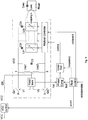
- FIG. 3 the block diagram of a series push-pull oscillator with a controlled capacity in the resonant network.
- This oscillator is used here as a base unit in a wireless feed system, but it can be used as an arbitrary oscillator.
- the switches Qv1 and Qv2 form a series-balanced (half-bridge) stage which alternately switches its midpoint to either VCC 'or to a reference potential (ground).
- the switches Qv1 and Qv2 are always open or closed alternately.
- the switches Qv1 and Qv2 are the same types (either two P-channel or two N-channel MOSFETs, or either two PNP or two NPN IGBTs).
- the in-phase drive signals V1 and V2 are guaranteed by the inverter (Inv).
- the switches Qv1 and Qv2 are complementary types (P / N channel MOSFETs and PNP / NPN bipolar transistors or IGBTs respectively) where Inv is not implemented.
- the switch center is connected to a series resonant circuit consisting of one or more inductors L01 ... L0n and one or more controlled capacitances Ctot with a reference potential (ground). At least An inductance L01 is active in the resonant circuit. If multiple inductors are used, any number of them are coupled to the resonant circuit via switches Q01 ... Q0n.
- a load unit comprises a load resistor (Rload), an off-hook inductance (Lsec), and often, but not necessarily, a capacitor Csec, which tunes a load unit to the resonant frequency of the base unit.
- Rload load resistor
- Lsec off-hook inductance
- Csec capacitor
- a parallel resonant circuit is also used in the load unit (not shown). The tuning in the load unit takes place on series or parallel resonance, but it is not critical because the attenuation of Rload increases the bandwidth significantly.
- the inductors L01 ... L0n are implemented as open coils and couple one or more load units to the base unit resonant circuit. If several inductors L01 ... L0n are used, they are positioned on one surface or on several surfaces that are at an angle to each other. If the corresponding coupling switch Q01... Q0n is closed, the current through the corresponding inductance L01... L0n generates an induction vector.
- the induction field can be distributed arbitrarily on a surface or a limited space.
- the radiated induction field is concentrated in this way on the positions of the load units. Thus, only those inductors L01 ... L0n are coupled to the resonant network, which transmit power to the load units.
- inductors L01 ... L0n coupled to the resonant network.
- inductor L01 which is permanently wired to the resonant network, is used in the power transmission.
- the arrangement can be considered in the near field as an open transformer whose coupling (coupling k) strongly with the geometric positioning and with the Distance from L01 ... L0n to Lsec varies.
- a feedback closes a feedback loop from the resonant network to the switch input V1 or V2. At a pole of the impedance formed by L01 ...
- the switches and the feedback block together also have zero degrees in their transfer function.
- the phase condition is fulfilled so that a sustained vibration can occur.
- the amplitude condition is also satisfied because the resulting attenuation by Rload is less than the gain of the loop (Qv1, Qv2, resonance network and feedback).
- the feedback block extracts a partial current from the resonant network and generates a rectangular driver signal for V1 or V2. This driver signal is additionally tapped and forwarded to a phase locked loop (PLL) as a fist.
- PLL phase locked loop
- phase comparator Compares fist with a reference frequency (fsoll) and filters the resulting error signal in the loop filter. The filtered error signal thus controls the capacitance of the resonant network Ctot.
- VCO Voltage Controlled Oscillator
- the filtered error signal regulates the capacitance Ctot until the oscillator frequency (fist) is again the same as the reference frequency (fsoll).
- the oscillator frequency fist
- the reference frequency fsoll
- different inductance values L01... L0n changes in the load unit, component value changes and changing coupling conditions are compensated.
- the phase error rate is determined by the response time of Ctot and the stability in the PLL.
- Ctot has a response time of half a resonant circuit period.
- the PLL loop can be dimensioned so that they is closed again as soon as possible if it disengages.
- the operating voltage VCC ' is controlled in block VCC control by pcont.
- the oscillator or resonance network current / voltage amplitude and consequently the energy of the radiated induction field is controlled.
- Coilselect controls the switches Q01 ... Q0n and corresponds to a selection signal of the inductors L01 ... L0n, which are coupled to the resonant network.
- Coilselect controls the geometric induction field distribution.
- the block Radicontrol generates the required signals pcont, coilselect, fsoll and loopselect.
- the radiationdata control signal contains parameters required for the generation of pcont, coilselect, fsoll and loopselect.
- Radiationdata contains a first data group, which is required for the generation of pcont. These are data that directly define pcont and / or data that defines how pcont should change over time. Thus Radicontrol generates a control signal (pcont) for VCCcontrol based on a first value of the first data group, which generates pulses to VCC 'and accordingly results in a burst operation in the oscillator. Further generates Radicontrol based on another value of the first data group Control signal (pcont) for VCC control, which allows VCC 'and accordingly the radiated field energy to be changed continuously. Radiationdata contains a second data group, which is required for the generation of coilselect.
- Radiationdata contains a third set of data required to generate fsoll. These are data that directly define fsoll and / or data that defines how fsoll should change over time.
- Radicontrol generates loopselect based on the signal coilselect and if fsoll changes more than one threshold (eg 10%) also based on fsoll. Loopselect modifies the PLL loop gain within the Loopfilters by means of z. Ex. Modifying the charge pump current in the output of the phase comparator. Is z.
- the radiated field energy can be controlled by pcont at any spectral position (fsoll) and at any spatial position. It can be created with a simple modification of radiationdata another radiation image. So z. For example, country-specific reduced field emission values can be generated at arbitrary spectral positions in a simple manner.
- Radicontrol continuously modifies the reference frequency (fsoll) (sweep) and, in another embodiment, stochastically to distribute the induction field spectrally. This is implemented taking into account frequencies not to be used fsoll.
- this reduces the maximum amount in the frequency spectrum and higher powers can be transmitted until the maximum limit value of the guidelines defined by the legislator has been reached.
- other users of the same frequency range are less disturbed and can thereby share the frequency range better.
- several users can negotiate the frequency range among themselves, so interference among each other will be minimal.
- the big advantage of frequency tracking circuits by means of phase locked loop (PLL) is the independence of the oscillator amplitude. In it, the oscillator always oscillates under its ideal conditions (phase and amplitude condition). Consequently, the radiated induction field remains unchanged at frequency changes unchanged.
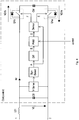
- FIG. 4 shows a block diagram of a controlled large signal capacity (Ctot (control)) according to FIG. 3 , Signal waveforms too FIG. 4 are in FIG. 5 and are used in the further description with its indices.
- the coupling to the oscillator takes place via the terminals 1 and 2.
- the inductance L01 shown here as one of several inductors L01 ... L0n
- the capacitor CM is coupled to C0 via the coupling switches Q1a and Q1b.
- the diodes indicated indicate that the coupling switches can only be controlled in one direction. In opposite current direction Q1a and Q1b remain bridged by the diodes.
- the term switch functionally defines the actively controllable part of Q1a and Q1b.
- the term coupling switch functionally defines the actively controllable part and the diode.
- the first Extremal condition of the switch control adjusts when the coupling switches Q1a and Q1b are always open. Then the resulting total capacity is equal to C0 and thus minimal. Accordingly, the resonant circuit frequency is maximum.
- the second extremal condition of the switch control adjusts when the coupling switches Q1a and Q1b are always closed. Then the resulting total capacity is equal to the parallel circuit of C0 and CM and thus maximum. Accordingly, the resonant circuit frequency is minimal.
- Partial interval coupling means that C0 and CM are coupled together during part of the resulting resonant circuit period. This is to be understood in the following description as a time or angle interval.
- the entire circuit represents a total capacity (Ctot) whose value is controlled by Control.
- the resonant circuit frequency results as the mean value of the entire resonant circuit period.
- the instantaneous resonant circuit frequency changes within the oscillating circuit period between minimum and maximum or maximum and minimum frequency according to the states of the two coupling switches.
- the resulting capacitor voltage V0 is tapped in block V-sense and then fed to the block Sign Detect for sign determination.
- the tapping of the capacitor voltage may also comprise only a partial voltage, it is only important that the sign of the output signal has a defined phase reference to the voltage V0 across the capacitor C0.
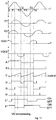
- the resulting waveform is shown in A.
- the subsequent differentiator (Diff) derives A by time and outputs its magnitude, see curve B. This gives positive pulses at each zero crossing 0, T3 and T6 of the resonant circuit voltage V0.
- the pulse width modulator (PWM) generates a sawtooth C in synchronism with the pulses of B (in FIG. 4 not shown, as it is a signal within the PWM modulator). This sawtooth curve C is compared within the PWM block with the control variable control. If control is less than C, the PWM output D is high.
- control is greater than C, then the PWM output D low.
- PWM pulse width modulation
- the modulator can be realized in various ways. It is only important that the PWM signal D is triggered by B and controlled by control in its pulse length. This pulse length corresponds to a controlled delay, which is controlled by the triggering torque (signal B) on control.
- the subsequent block Demux selects a portion of the corresponding half wave using signal A and supplies it to the switches Q1a and Q1b. If A is high, the negated signal D controls the switch Q1a via E. If A is low, the negated signal D controls the switch Q1b via F. If D via A is not linked to the corresponding output E or F, E or F remains high.
- the switch Q1a or Q1b is closed (ON) when E or F is high. If E and F are deep, then Q1a and Q1b are open. The switches always remain closed for at least one half-cycle and bridge their internal diode. This results in smaller forward losses and prevents transient transients from occurring when the diodes are turned on. The diodes can still carry a certain residual current. In any case, the method causes a reduction in losses, especially when the on-resistance of the switches (Rdson) is sufficiently small.
- FIG. 6 a ParallelGegentakt oscillator, which provides over the half-bridge with the same circuit complexity more power.
- a symmetrically tapped coil (Ltap1 and Ltap2) is alternately switched at each end via a switch (Qv1 and Qv2) to a reference potential (ground).
- Qv1 and Qv2 a switch
- Qv1 and Qv2 a switch
- L0 controlled inductors
- auxiliary inductors L01 ... L0n are coupled to Ltap1 and Ltap2. This is implemented alternatively via additional series capacities (not shown).
- the capacitance C0 forms a parallel resonant circuit with Ltap1, tap2, L0 and L01 ... L0n. If several inductors L01 ... L0n are used, any number of them can be coupled to the resonant circuit via switches Q01 ... Q0n. In this case, additional series inductances and their switches can be implemented in any branch Q0n, L0n (not shown). These switches bridge depending on the control Series inductors. Such extended inductance arrangements may be required at high VCCs, higher transmittable powers, and / or more load units.
- a load unit comprises a load resistor (Rload), an off-hook inductance (Lsec), and often, but not necessarily, a capacitor Csec, which tunes a load unit to the resonant frequency of the base unit.
- Rload load resistor
- Lsec off-hook inductance
- Csec capacitor
- the tuning in the load unit takes place on series or parallel resonance, but it is not critical because the attenuation of Rload increases the bandwidth significantly.
- All or any number of inductors Ltap1, Ltap2, L0, L01 ... L0n are implemented as open coils and couple one or more load units to the resonant circuit of the base unit. If several inductances Ltap1, Ltap2, L0, L01 ...
- L0n are used, they are positioned on one surface or on several surfaces which are at an angle to one another. If the corresponding coil coupling switch Q01 ... Q0n closed, the current generated by the corresponding inductance L01 ... L0n an induction vector.
- the induction field can be distributed arbitrarily on a surface or a limited space.
- the radiated induction field is concentrated on the positions of the load units. Thus, only those inductors L01 ... L0n are coupled to the resonant network, which transmit power to the load units. If only one load unit is present, its coupling to the base unit can be improved by multiple inductors L01 ... L0n coupled to the resonant network.
- the arrangement can be considered in the near field as an open transformer whose coupling (coupling k) varies greatly with the geometric positioning and with the distance from Ltap1, Ltap2, L0, L01 ... L0n to Lsec.
- the feedback closes a feedback loop from the resonant network to the switch input of Qv1 and Qv2.
- the coil DR wicks as a filter in the feed line, reducing the harmonic distortion of the push-pull stage (Qv1, Qv2).
- DR acts as a current source on the tap point, thus causing full-wave rectification voltage, the average of which is equal to VCC ', at the tap point.
- the Minimum value of the voltage at the tap corresponds to the voltage zero crossing of the voltage above C0.
- This voltage zero crossing or the minimum value of the voltage at the tapping point of the coils Ltap1, Ltap2 triggers a frequency divider within the feedback block.
- the inverted or non-inverted output of the frequency divider controls Qv1 and Qv2, respectively.
- Is z For example Qv1 closed and Qv2 open, a sinusoidal voltage half-wave forms at the input of the feedback block with half the voltage amplitude of the voltage over C0.
- the frequency divider is triggered and the drive signals of Qv1 and Qv2 change states.
- Qv2 is closed and Qv1 is open. It again forms a sinusoidal voltage half wave with half the voltage amplitude of the voltage across C0.
- phase comparator Phase Comp.
- fsoll reference frequency
- the error signal from the block Phase Comp. is then filtered in the block Loopfilter.
- the filtered error signal controls the inductance L0 of the resonant network. If the oscillator does not oscillate to fsoll, or if the reactance in the oscillator detunes, an error signal is produced at the output of the phase comparator (Phase Comp.).
- the filtered error signal regulates the inductance L0 until the oscillator frequency (fist) is again the same as the reference frequency (fsoll).
- the oscillator frequency fist
- fsoll reference frequency
- different inductance values L01... L0n changes in the load unit, component value changes and changing coupling conditions are compensated.
- the settling speed is determined by the response time of L0 and the stability in the PLL.
- L0 has a response time of half a resonant circuit period.
- the PLL loop can be dimensioned so that it is closed again as soon as possible once it disengages.
- FIG. 7 shows the block diagram of a controlled large signal inductance (L0 (control)) according to FIG. 6 .
- L0 control
- Signal waveforms too FIG. 7 are in FIG. 8 and are used in the further description with its indices.
- the coupling to the oscillator takes place via the connections 1 and 2.
- the resulting total inductance Ltap (from Ltap1 and Ltap2) in FIG. 7 shown. It forms a parallel resonant circuit together with the capacitance C0.
- the inductance LM is coupled to Ltap via the coupling switches Q1a and Q1b.
- the first extremal condition of the switch control adjusts when both coupling switches Q1a and Q1b are always open. Then the resulting total inductance is equal to Ltap and thus maximum.
- the resonant circuit frequency is minimal.
- the second extremal condition of the switch control adjusts when both coupling switches Q1a and Q1b are always closed. Then the resulting total inductance is equal to the parallel connection of Ltap and LM and thus minimal. Accordingly, the resonant circuit frequency is maximum.
- any intermediate value of the two extreme values for the total inductance can be set via the control input control.
- the entire circuit represents a total inductance (L0) whose value is controlled by control.
- the resonant circuit frequency results as the mean value of the entire resonant circuit period.
- the instantaneous resonant circuit frequency changes within the oscillating circuit period between minimum and maximum or maximum and minimum frequency according to the states of the two coupling switches.
- the resulting coil current is tapped in block I-sense and then fed to the block Sign Detect for sign determination.
- the tapping of the coil current may also comprise only a partial current of I0, it is only important that the sign of the output signal has a defined Phase reference to the current I0 in the coil Ltap has.
- the resulting waveform is shown in A.
- the subsequent differentiator (Diff) derives A by time and outputs its magnitude, see curve B. This gives positive pulses at each zero crossing 0, T3 and T6 of resonant circuit current I0.
- the pulse width modulator (PWM) generates a sawtooth C in synchronism with the pulses of B (in FIG. 7 not shown, as it is a signal within the PWM modulator). This sawtooth curve C is compared within the PWM block with the control variable control. If control is less than C, the PWM output D is high. If control is greater than C, the PWM output D is low. Based on the known pulse width modulation (PWM), the modulator can be realized in various ways. It is only important that the PWM output signal D is triggered by B and is controlled by control in its pulse length. This pulse length corresponds to a controlled delay, which is controlled by the triggering torque (signal B) on control.
- the V-Sense block picks up the voltage via Ltap and the Sign Detect block detects the sign of this voltage, see signal J.
- the following differentiator (Diff) derives J by time and outputs its magnitude, see curve K. This yields positive pulses at each zero crossing of the resonant circuit voltage V0 (see V0 zerocrossing in Figure 8 ).
- the pulses of signal K coincide in time with the maxima or minima of the current I0.
- the signal K is connected to A and D in demux to generate the drive signals E 'and F' of the switches Q1a and Q1b.
- the switch Q1a or Q1b is closed (ON) when E 'or F' is high. If E 'or F' is low, Q1a or Q1b is open.
- the diodes can still carry a certain residual current.
- the method causes a reduction in losses, especially when the on-resistance of the switches (Rdson) is sufficiently small.
- the coupling switch Q1a closes and a sinusoidal current half-wave develops in IM.
- the total coupling switch voltage VQ1 VQ1a + VQ1b is zero because both coupling switches are closed.
- the current IM becomes zero again at time T2
- the stored energy in C0 forces a negative voltage jump in the internal diode of Q1b and consequently an interruption of the current flow.
- FIG. 9 a parallel push-pull oscillator according to FIG. 6
- the frequency control here comprises not only a controlled inductance but at least one or more series circuits C01, L01 ... C0n, L0n, which are coupled via switches to the parallel resonant circuit (Ltap1, Ltap2 and C0).
- the switches are integrated here in the block Multicoil Controller and they are used for frequency and induction field control.
- the corresponding input signals are the output of the Loopfilters (control) and coilselect from the block Radicontrol.
- the filtered error signal (control) controls one or more series circuits C01, L01 ...
- the settling speed is determined by the response time of the series circuits C01, L01 ... C0n, L0n and the stability in the PLL.
- the series circuits C01, L01... C0n, L0n have a response time of half a resonant circuit period.
- the PLL loop can be dimensioned so that it is closed again as soon as possible once it disengages.
- the blocks VCC control and Radicontrol as well as their input and output signals behave identically to their identically named in FIG. 3 , This means that the same operating modes have been implemented. All the inductors (L01 ... L0n) coupled to the oscillator and, alternatively, Ltap1, Ltap2 contribute to the energy transfer.
- the oscillator is functional with FIG.
- the coupling switch control of the resonant network according to FIG. 9 is in FIG. 10 shown.
- the corresponding signals are in FIG. 11 and are used in the further description with their indices.
- the coupling to the oscillator takes place via the connections 1 and 2.
- the resulting total inductance Ltap (from Ltap1 and Ltap2) in FIG. 10 shown. It forms a parallel resonant circuit together with the capacitance C0.
- One or more series circuits C01, L01 ... C0n, L0n are coupled to Ltap via one or more coupling switches Q01 ... Q0n.
- the first extremal condition of the switch control adjusts when all the coupling switches Q01 ... Q01n are always open.
- the resulting total inductance is equal to Ltap and thus maximum. Accordingly, the resonant circuit frequency is minimal.
- the second extremal condition of the switch control adjusts when all the coupling switches Q01 and Q01n are always closed. Then the resulting total inductance is minimum and equal to the parallel connection of Ltap and the resulting inductance of all series circuits C01, L01 ... C0n, L0n. Accordingly, the resonant circuit frequency is maximum.
- the series circuits C01, L01... C0n, L0n are dimensioned so that their serially resonating for continuously closed switches Q01... Q01n is lower than the lowest network frequency or lowest oscillator frequency.
- the series circuits act as inductors, and thereby the total inductance of the overall network can be controlled.
- any intermediate value of the two extreme values for the total inductance can be set via the control input control.
- the resonant circuit frequency results as the mean value of the entire resonant circuit period.
- the instantaneous resonant circuit frequency changes within the resonant circuit period corresponding to the states of the coupling switch.
- the resulting coil current is tapped in block I-sense and then fed to the block Sign Detect for sign determination.
- the tapping of the coil current may also comprise only a partial current of I0, it is only important that the sign of the output signal has a defined phase reference to the current I0 in the coil Ltap.
- the resulting waveform is shown in A.
- the subsequent differentiator (Diff) derives A by time and outputs its magnitude, see curve B. This gives positive pulses at each zero crossing 0, T3 and T6 of resonant circuit current I0.
- the pulse width modulator (PWM) generates a sawtooth C in synchronism with the pulses of B (in FIG. 10 not shown, as it is a signal within the PWM modulator). This sawtooth curve C is compared within the PWM block with the control variable control. If control is less than C, the PWM output D is high.
- the modulator can be realized in various ways. It is only important that the PWM output signal D is triggered by B and is controlled by control in its pulse length. This pulse length corresponds to a controlled delay, which is controlled by the triggering torque (signal B) on control.
- the block V-sense seizes the voltage via Ltap and the block Sign Detect detects the sign of this voltage, see signal G.
- the following differentiator (Diff) derives G by time and outputs its magnitude, see curve H. This yields positive pulses at each zero crossing of the resonant circuit voltage V0 (see V0 zerocrossing in Figure 11 ).
- the pulses of signal H coincide in time with the maxima or minima of the current I0.
- the signal H is associated with A and D in demux to generate the drive signals E “and F” for the switches Q01 ... Q0n.
- the drive signals E “and F” are coupled via the AND gates A01 ... A0n to the corresponding coupling switches.
- E "is identical to 01, 03 ... 0n-1 and F” is identical to 02, 04 ... 0n if coilselect releases all ANDs A01 ... A0n on E "and F”.
- the corresponding selection signals coil 01 select ... coil 0n select are coupled by means of signal A to the corresponding inputs of the ANDs. In this way you can change coil 01 select ... coil 0n select at any time.
- a stable driver signal 01 ... 0n always sets in at each network period.
- the switches Q01 ... Q0n are closed (ON) when E “or F” is high. If E “or F” is low, Q01 ... Q0n are open. If A is high, the signal D over E “controls the closing of switch Q01 (see time T1). If A is low, the signal D over F” controls the closing of switch Q02 (see time T4). The transition from high (ON) to low (OFF) in E “and F” controls signal H with A, see times V0 zerocrossing in E “and F”. The signal A selects which switch is controlled. If A is low, switch Q01 opens via E “with H. If A is high, switch Q02 opens via F” with H.
- the switches are always closed for at least one half-cycle, at least partially bypassing their internal diodes. This results in smaller forward losses and prevents transient transients from occurring when the diodes are turned on.
- the diodes can still carry a certain residual current. In any case, the method causes a reduction in losses, especially when the on-resistance of the switches (Rdson) is sufficiently small.
- the coupling switch Q01 closes and a current wave develops in I01
- This current wave defines a coupling period which is twice as long as the interval from T1 to T3 During this entire coupling period, the coupling switch voltage VQ01 is equal to zero At time T3 Further, the current I01 is zeroed at time T3 and then discharges the capacitor C01 with a negative current I01 at the interval T3 to T5, and the current I01 becomes zero again at time T5 , the current flow I01 to E "stops again coupling the series circuit C01, L01 to the rest of the resonance network.
- the coupling switch Q02 closes and a current wave develops in I02
- This current wave defines a coupling period which is twice as long as the interval from T4 to T6 Throughout this coupling period, the coupling switch voltage VQ02 equals zero
- T6 is the whole Energy of the series circuit C02, L02 stored in C02.
- the current I01 passes through the zero point at time T6 and then discharges the capacitance C02 with a positive current I02 in the following coupling half period.
- This coupling half-period is identical to the interval from 0 to T2.
- an inductance (L01... L0n) with only one active element (with only one switch) can thus be driven with a symmetrical current wave.
- the radiation fields in the two inductors L01 and L02 compensate each other. It is further easy to determine that even with a switch (Example Q01) and a series circuit (Ex: C01, L01) results in a symmetrical to the zero line current curve. This results in less Hardware expenditure more favorable spectral distributions (fewer harmonics or smaller distortions) FIG. 6 ,
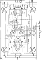
- FIG. 12 shows a detail circuit of a Parallelumbletakt large signal VCOs according to the current invention.
- the oscillator essentially corresponds to that of the FIGS. 6 and 9 , Ltap1, Ltap2 are in one embodiment, the radiation coils of the induction vector (or at least part of it).
- Ltap1, Ltap2 are in one embodiment, the radiation coils of the induction vector (or at least part of it).
- At the ends of the coupled inductance Ltap1, Ltap2 is a respective switch Qv1 and Qv2 to ground.
- the operating voltage is supplied via DR from VCC control here as Switched Mode Power Supply (SMPS).
- SMPS Switched Mode Power Supply
- the resonant circuit is connected. This is a controlled capacity in the simplest case. In another embodiment, these are controlled capacitances / inductors or controlled series circuits of the two.
- RV9 and CV6 form a low pass that attenuates transients.
- QV7, DV3 and RV7 form the voltage minimum detector whose reference voltage is applied to the emitter of QV8 filtered with CV5. The reference voltage is determined by the voltage divider RV6 and RV8.
- QV9 is only responsible for the oscillation and thus always in the normal mode via RV5 conductive.
- the reference voltage is proportional to the average of the input voltage.
- QV7 opens regardless of the output voltage from the SMPS at the minimum voltage via CV6.
- the resulting pulses at the collector QV7 triggers the flip-flop FFV. This causes its outputs Q and IQ to flip. This drives the driver transistors QV3 ...
- the trigger signal from FFV is coupled to the phase comparator (Phase Frequency Detector PFD) as a fist.
- the reference frequency (fsoll) is a controlled frequency divider (RefDiv) of a reference frequency (fref) z. Eg 32MHz derived.
- the PFD corresponds to that of the known circuit of the CMOS module 4046.
- the PFD output signals are fed independently via the resistors RP1... RP4 via a respective current mirror QV8, QV10 or QV7, QV9 to the loop filter CP1, CP2 and FP7 coupled.
- Transconductance amplifier QV11 generates the control current for the controlled admittances in proportion to the control voltage across the loop filter.
- the PLL loop gain is switched via the analog switch SW. This changes the charge pump current of QV9 and QV10, which flows into the loop filter.
- FIG. 13 shows a detail circuit of a controlled capacity according to the block diagram of FIG. 4 ,
- the dashed lines comprise parts of the block diagram.
- waveforms of FIG. 5 referenced with their indexes.
- CM is implemented as a series connection of 2 capacitors CM1 and CM2, which is coupled to C0 via Q1a and Q1b.
- the switch control is operated on a supply voltage +12 '.
- An optocoupler (OPTO) transmits the control information (control) galvanically isolated, since the switch control galvanic by +12 'from the rest of the network is disconnected.
- OPTO optocoupler
- the capacitors C1 and C2 pick up the positive voltage half-wave from V0 and feed it via R1 to the base of transistor Q10.
- Q10 acts as a quasi voltage zero-point detector of the positive half wave.
- D1 and D3 accelerate the shutdown as soon as the voltage across C2 falls below the threshold voltage of Q10.
- the capacitive voltage divider C1, C2 prevents DC coupling to V0.
- a phase predistortion can be achieved via R1, C1 and C2.
- these components are dimensioned so that the Phasenwordrehung is at least as large as the total signal delay of the control circuit. This makes it possible to use the entire control range.
- the components Q9, D2, D4, R3, R4, C3 and C4 work identically to the components around Q10, only they are responsible for the negative half wave of V0.
- the two D flip-flops FF1, FF2 and the NAND gate N1 detect the two positive edges of the output signals of the voltage zero point detectors Q9 and Q10.
- a flip-flop (FF1 or FF2) alternately switches on the Q output as soon as it is triggered on the Clock CK. This state is immediately reset after the runtime of N1 via the corresponding reset input.
- voltage pulses occur at each zero crossing of V0 (signal curve B), which briefly completely drive through the transistor Q2.
- FF5 is configured via the pulses on the set (S) or reset (R) input in such a way that the sawtooth always uses the corresponding switch controls, which is responsible for the corresponding half-wave. This corresponds to the switching signal selection by means of signal curve A. If V0 appears with the positive half-wave, D2 is conducting. The collector of Q9 is high and triggers FF2 over CK. The briefly set output Q of FF2 sets the output Q of FF5 via its set (S) input. The low at the output IQ of FF5 forces a high at the output of N4, which closes Q1a via the drivers Q3, Q4. This is the initial condition for the controlled decoupling of CM1 and CM2 during the positive half cycle of V0.
- FIG. 14 shows a detail circuit of a controlled series circuit of inductance and capacitance according to the block diagram of FIG. 10 ,
- the dashed lines comprise parts of the block diagram.
- waveforms of FIG. 11 referenced with their indexes.
- L01, C01, L02, C02, L03, C03 and L04, C04 are coupled to C0 via Q01 ... Q04.
- the required control signals 01 ... 04 of the coupling switches Q01 ... Q04 are electrically isolated from the outputs of the NAND gates N3 ... N6 via the transformers T1 ... T4 to Q01 ... Q04.
- optocouplers with subsequent driver can be used (not shown).
- the NANDs N3 ... N6 constitute the multiplexer which selects the switch control outputs of the flip-flops FF5 and FF6 depending on the selection signals coil 01 select and coil 02 select latched by FF7 and FF8. If coil 01 select or coil 02 select is high, the corresponding NANDs (N3, N4 or N5, N6) are transparent and loop through the output signals from FF5 and FF6 to the corresponding pair of coupling switches (Q01, Q02 or Q03, Q04). In a further embodiment, all 4 inputs of NANDs N3 ... N6 can be selected via 4 control lines coil 01 select ... coil 04 select. The switch control is operated at a voltage +12 with any reference potential.
- Inductor L1 picks up the positive current half-wave of I0 and supplies it via R1 and C2 to the base of transistor Q10.
- Q10 acts as a quasi-current zero-point detector of the positive half-wave.
- D1 and D3 accelerate the shutdown as soon as the current through C2 changes its sign. Further, C2 prevents DC coupling to I0.
- the current sense network is designed such that a phase predistortion results. This makes it possible to use the entire control range.
- the components Q9, D2, D4, R3, C4 and L2 work identically to the components around Q10, but they are responsible for the negative current half-wave of I0.
- the two D flip-flops FF1, FF2 and the NAND gate N1 detect the two positive edges of the output signals of the current zero detectors Q9 and Q10. To do this, switch on alternately Flip-flop (FF1 or FF2) at output Q high as soon as it is triggered at the clock CK. This state is immediately reset after the runtime of N1 via the corresponding reset input. Thus, at the output of N1, voltage pulses occur at each zero crossing of I0 (signal curve B), which briefly completely drive through the transistor Q2.
- This symmetric implementation guarantees identical behavior with respect to the two current half-waves of I0.
- Q2 is coupled to I0 only during the triggering moment of the short voltage pulses.
- Q7, Q8, R6 and R5 reflect a control current which flows into the capacitor C5 and is controlled by terminal 3 (control) from the loop filter.
- the result is a sawtooth voltage across C5 (curve C), which reaches its lowest value in time with the modulation pulses of Q2.
- This sawtooth voltage triggers FF5 via input CK as soon as its switching threshold is reached. This point in time can be controlled via the control input control because the slope of the sawtooth voltage can be changed by the collector current in Q8 and consequently by control.
- FF5, FF6, N3 and N4 constitute the demux.
- FF5 is configured via the pulses on the set (S) or reset (R) input so that the sawtooth always triggers the corresponding switch, which is responsible for the corresponding half-wave.
- FF5 tilts and its output Q goes low. Since IQ of FF6 remains high, the outputs of N4 and N6 will go high, thus coupling switches Q01 and Q03 will close via drivers Q3, Q4 and Q15, Q16 if coil 01 select and coil 02 select are high. The same happens with the negative half wave of I0.
- the inverted output FF5's IQ is set via the Reset (R) input of FF1 as soon as D1 is conductive and FF1 is triggered via the Clock (CK).
- the advantage of the differentiation is the robustness to transients, which disturb the function only after a change of sign of the total voltage (V0). This makes the "turn off command" of switches Q01 ... Q04 insensitive to transients of the resonant circuit.
- the flip-flop FF6 synchronizes itself, at the latest one oscillation cycle period after switching on the entire circuit.
- the capacitances C01 ... C04 are not populated and replaced by bridges in FIG. 14 , Then, the VCO corresponds to the embodiment according to FIGS. 7 and 8th with several inductances.
- the controller in FIG. 12 generates pcont, coilselect (containing the signals coil 01 select and coil 02 select) and fsoll according to the input data contained in radiationdata. Loopselect is generated by the data coilselect. In another embodiment, loopselect is generated based on the data coilselect and RefDivvalue. RefDivvalue shares fref and thus generates fsoll. In one embodiment, RefDivvalue is unchanged in time and generates a discrete VCO spectral line (measured according to EN300330). This spectral line is controlled by the controller via Refdivvalue and fsoll according to data within radicontrol. Fsoll is constant in it during an energy transfer interval.
- An energy transfer interval is a time-limited segment characterized by an induction vector (measured current in a radiation coil) that is greater than 1 ... 10% of its maximum possible value.
- RefDivvalue changes in time and distributes an induction vector (measured current in a radiation coil) to at least two spectral positions.
- RefDivvalue or fsoll changes so fast that an induction vector (measured current in a radiation coil) is distributed over several spectral lines or one spectral range (measured according to EN300330).
- the controller generates RefDivvalue values, which output consecutively random values from a minimum and maximum limited value range. These values are generated according to a pseudo random sequence (PRS) and describe a sine (x) / x in at least one partial spectrum of the induction vector spectrum (measured current in a radiation coil).
- the controller RefDivvalue generates values which output a continuous sweep sequence as values from a minimum and maximum limited value range. A sweep sequence is characterized in that the output values change periodically from a minimum value to the maximum value and then from the maximum value to the minimum value and so on.
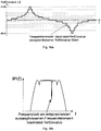
- Figure 15a shows a period of such a sweep sequence (RefDivvalue (t)), wherein the dwell time (time interval which outputs the same RefDivvalue) changes dynamically on the time axis (t) in dependence on RefDivvalue.
- the dwell time time interval which outputs the same RefDivvalue
- the dwell time changes dynamically on the time axis (t) in dependence on RefDivvalue.
- the dwell time time interval which outputs the same RefDivvalue
- the dwell time time interval which outputs the same RefDivvalue
- RefDivvalue not all possible Refvalval values are output in RefDivvalue (t). So will be like in FIG. 16a shown, the value "blacklisted RefDivvalue" not used in the sweep sequence. As a result, fsoll does not generate frequency at point fref divided by "blacklisted RefDivvalue". This also results in no spectral component at the corresponding location in the VCO frequency. In this way, any cuts can be made in IPI max (f) (see FIG. 16b ). It is clear that yourself apply this procedure to any RefDivvalue (t) sequence, whether it is a sweep sequence or a PRS.
- the controller in FIG. 12 generates in one embodiment pcont- and fsoll values, which results in an arbitrary spectral distribution including cuts (eg according to EN300330, REC7003 and ITU-RSM2123).
- Pcont is either determined by the power control between the base unit and the load unit or, if necessary, limited by maximum values of the standards mentioned.
- corresponding RefDivvalues (min, max and one or more blacklist RefDivvalue) are stored as parameters in a memory.
- a memory stores parameters for pcont and parameters that determine the dwell time of RefDivvalue (t).
- the controller can be implemented as a discrete digital network, integrated logic circuit (PLD, FPGA) or as a microcontroller.
- RAM / ROM memories are integrated in integrated circuits (PLD, FPGAs and microcontrollers with integrated memory).
- data input / output interfaces such as eg pcont, radiationdata, coilselect and refdivvalue
- the controller implementation can be implemented extremely compact and cost-effective, depending on your requirements.
- All of the LC based AC generators and all LC oscillator capabilities may be built in conjunction with controlled capacitances and / or controlled inductors and / or controlled combination circuits of both.
- the term “L” stands for inductance or coil and the term “C” stands for capacitance or capacitor.
- the simplest embodiment of the current invention is an AC voltage generator with a tunable resonant network. In this embodiment, one simply leaves the feedback block in the Figures 3 . 6 and 9 path.
- the switches Qv1 and Qv2 are controlled by any external signal.
- the independent (decoupled from the oscillator) Drive signals (V1 and V2) give a higher freedom in the generator design.
Landscapes
- Engineering & Computer Science (AREA)
- Power Engineering (AREA)
- Computer Networks & Wireless Communication (AREA)
- Signal Processing (AREA)
- Inductance-Capacitance Distribution Constants And Capacitance-Resistance Oscillators (AREA)
Claims (13)
- Un générateur de tension alternative ou de courant alternatif dont le réseau de sortie peut être ajusté en fréquence, le réseau de sortie comprenant un réseau résonnant dont l'amplitude du courant / de la tension du réseau résonnant est contrôlée, comprenant:a) au moins un premier commutateur (Qv1) qui est commandé par une tension alternative numérique ou un courant alternatif numérique et dont la charge comprend un réseau résonnant ayant au moins une première inductance (Ltap) et au moins une première capacité (C0),b) au moins une deuxième inductance (LM) ou au moins une deuxième capacité (CM) ou au moins un circuit série d'une troisième inductance (L01) et d'une troisième capacité (C01) qui est couplé au réseau résonnant par au moins un deuxième commutateur au moyen d'un signal de couplage ON/OFF (E, E', E", F, F', F"), dans laquelle la deuxième inductance (LM) ou la deuxième capacité (CM) ou le circuit série de la troisième inductance (L01) et de la troisième capacité (C01) est chargé et déchargé par le réseau résonnant et le signal de couplage ON/OFF (E, E', E", F, F', F") change au moins une fois pendant la période du réseau résonnant et est caractérisé en ce quel'au moins un deuxième commutateur est commandé avec un retard controllé (PWM) qui est synchronisé par un changement de signe du courant et/ou de la tension dans le réseau résonnant, et l'amplitude du courant / de la tension du réseau résonnant de la tension alternative ou du générateur de courant alternatif est commandée indépendamment du réglage de la fréquence par un moyen (commande VCC, DR, SMPS) qui commande la tension de fonctionnement / le courant de fonctionnement du générateur de tension alternative ou de courant alternatif.
- Le générateur de tension alternative ou de courant alternatif selon la revendication 1, dans lequel la fréquence de résonance du réseau résonnant est régulée à une valeur prédéterminée (fsoll) dépendante d'une variable de contrôle (control) dans une boucle fermée.
- Le générateur de tension alternative ou de courant alternatif selon la revendication 1, dans lequel le premier commutateur comprend au moins deux commutateurs (Qv1, Qv2) qui forment un demi pont ou un pont complet ou un circuit push-pull parallèle, et l'amplitude du courant / tension du réseau résonnant du générateur de tension alternative ou de courant alternatif change continuellement ou établit le mode rafale par le moyen (control, VCC, DR, SMPS) déendante d'un signal de commande (pcont).
- Générateur de tension alternative ou de courant alternatif selon la revendication 1, dans lequel le signal de commande du premier et/ou du second commutateur est généré sur la base d'au moins un détecteur de tension ou de courant quasi nul (Q, 9, Q10 ou Q11, Q12 ou QV7, QV8) ayant la même valeur seuil pour la demi-onde positive et négative.
- Oscillateur dont l'amplitude et la fréquence courant / tension sont contrôlées comprenant:a) au moins une première inductance (Ltap) et au moins une première capacité (C0) couplées ensemble et formant au moins une partie d'un réseau résonant,b) au moins une deuxième inductance (LM) ou au moins une deuxième capacité (CM) ou au moins un circuit série d'une troisième inductance (L01) et une troisième capacité (C01),c) au moins un second commutateur commandé par un signal de couplage ON/OFF (E, E', E", F, F', F") pour coupler la seconde inductance (LM) ou la seconde capacité (CM) ou la connexion en série de la troisième inductance (L01) et la troisième capacité (C01) au réseau résonant via un retard contrôlé (PWM), dans lequel la charge et la décharge de la deuxième inductance (LM) ou de la deuxième capacité (CM) ou du circuit série de la troisième inductance (L01) et de la troisième capacité (C01) sont effectuées par le réseau résonnant, et le signal de couplage ON/OFF (E, E', E", F, F', F") change au moins une fois pendant la période du réseau résonnant, etd) au moins un premier commutateur (Qv1) caractérisé en ce quele au moins un premier commutateur (Qv1) est commandé numériquement et est couplé au réseau résonnant de telle sorte que le premier commutateur et le réseau résonnant fonctionnent comme oscillateur et que l'amplitude du courant / tension de l'oscillateur est commandée indépendamment de la commande de fréquence par un moyen (control, VCC, SMPS) qui commande la tension / le courant de fonctionnement de l'oscillateur.
- Oscillateur selon la revendication 5, dans lequel la fréquence de résonance du réseau résonnant est ajustée à une valeur prédéterminée (fsoll) dépendante d'une grandeur de commande (control) dans une boucle fermée.
- Oscillateur selon la revendication 5, dans lequel le premier commutateur comprend au moins deux commutateurs (Qv1, Qv2) qui forment un demi pont partiel ou un pont complet ou un circuit push-pull parallèle et l'amplitude du courant / tension du réseau de résonance de l'oscillateur change continuellement ou établit le mode rafale par les moyens (control, VCC, DR, SMPS) en fonctiond' un signal de commande (pcont).
- Oscillateur selon la revendication 5, dans lequel le signal de commande du premier et/ou du second commutateur est généré sur la base d'au moins un détecteur de tension ou de courant (Q, 9, Q10 ou Q11, Q12 ou QV7, QV8) ayant la même valeur seuil pour la demi-onde positive et négative.
- Oscillateur selon la revendication 5, le premier commutateur comprenant au moins deux commutateurs (Qv1, Qv2) et au moins un détecteur de tension (QV7) qui exploite symétriquement la rétroaction de l'oscillateur sur le réseau de résonance.
- Oscillateur dont l'amplitude et la fréquence courant / tension sont contrôlées, comprenant :a) au moins une première inductance (Ltap) et au moins une première capacité (C0) qui sont couplées l'une à l'autre et forment au moins une partie d'un réseau résonant,b) au moins une deuxième inductance (LM) ou au moins une deuxième capacité (CM) ou au moins un circuit série d'une troisième inductance (L01) et une troisième capacité (C01),c) au moins un second commutateur commandé par un signal de couplage ON/OFF (E, E', E", F, F', F") pour coupler la seconde inductance (LM) ou la seconde capacité (CM) ou la connexion en série de la troisième inductance (L01) et la troisième capacité (C01) au réseau résonant via un retard contrôlé (PWM), dans laquelle la charge et la décharge de la deuxième inductance (LM) ou de la deuxième capacité (CM) ou du circuit série de la troisième inductance (L01) et de la troisième capacité (C01) sont effectuées par le réseau résonnant, et le signal de couplage ON/OFF (E, E', E", F, F', F") change au moins une fois pendant la période du réseau résonnant, etd) au moins un premier commutateur (Qv1) caractérisé en ce quele premier commutateur (Qv1) est commandé numériquement et couplé au réseau résonnant de telle sorte que le premier commutateur et le réseau résonnant fonctionnent comme oscillateur et que le signal de commande du premier et/ou du second commutateur est généré sur la base d'au moins un détecteur de tension ou de courant quasi nul (Q,9, Q10 ou Q11, Q12 ou QV7, QV8) pour la détection des demi-ondes positives et négatives avec le même niveau de seuil et l'amplitude courant / tension de l'oscillateur est commandée par un moyen (control, VCC, SMPS) qui commande la tension / courant de fonctionnement de l'oscillateur.
- Oscillateur selon la revendication 10, dans lequel la fréquence de résonance du réseau résonnant est ajustée à une valeur prédéterminée (fsoll) dépendante d'une grandeur de commande (control) dans une boucle fermée et l'amplitude courant / tension de l'oscillateur est commandée indépendamment de la commande de fréquence par les moyens (control, VCC, SMPS).
- Oscillateur selon la revendication 10, dans lequel le premier commutateur comprend au moins deux commutateurs (Qv1, Qv2) qui forment un demi-pont ou un pont complet ou un circuit push-pull parallèle et l'amplitude du courant / tension du réseau de résonance de l'oscillateur change continuellement ou établit un mode rafale par le moyen (commande VCC, DR, SMPS) dépendant d'un signal de commande (pcont).
- Oscillateur selon la revendication 10, le premier commutateur comprenant au moins deux commutateurs (Qv1, Qv2) et au moins un détecteur de tension (QV7) qui exploite symétriquement la rétroaction de l'oscillateur sur le réseau résonnant.
Priority Applications (1)
| Application Number | Priority Date | Filing Date | Title |
|---|---|---|---|
| EP18000769.2A EP3460952B1 (fr) | 2011-04-04 | 2012-03-22 | Oscillateur régulé par tension pour grands signaux |
Applications Claiming Priority (1)
| Application Number | Priority Date | Filing Date | Title |
|---|---|---|---|
| DE102011016027A DE102011016027A1 (de) | 2011-04-04 | 2011-04-04 | Großsignal VCO |
Related Child Applications (2)
| Application Number | Title | Priority Date | Filing Date |
|---|---|---|---|
| EP18000769.2A Division-Into EP3460952B1 (fr) | 2011-04-04 | 2012-03-22 | Oscillateur régulé par tension pour grands signaux |
| EP18000769.2A Division EP3460952B1 (fr) | 2011-04-04 | 2012-03-22 | Oscillateur régulé par tension pour grands signaux |
Publications (3)
| Publication Number | Publication Date |
|---|---|
| EP2573904A2 EP2573904A2 (fr) | 2013-03-27 |
| EP2573904A3 EP2573904A3 (fr) | 2013-08-07 |
| EP2573904B1 true EP2573904B1 (fr) | 2018-12-05 |
Family
ID=46021961
Family Applications (2)
| Application Number | Title | Priority Date | Filing Date |
|---|---|---|---|
| EP12002023.5A Active EP2573904B1 (fr) | 2011-04-04 | 2012-03-22 | Oscillateur grand signal commandé en tension |
| EP18000769.2A Active EP3460952B1 (fr) | 2011-04-04 | 2012-03-22 | Oscillateur régulé par tension pour grands signaux |
Family Applications After (1)
| Application Number | Title | Priority Date | Filing Date |
|---|---|---|---|
| EP18000769.2A Active EP3460952B1 (fr) | 2011-04-04 | 2012-03-22 | Oscillateur régulé par tension pour grands signaux |
Country Status (3)
| Country | Link |
|---|---|
| US (3) | US8963514B2 (fr) |
| EP (2) | EP2573904B1 (fr) |
| DE (1) | DE102011016027A1 (fr) |
Families Citing this family (29)
| Publication number | Priority date | Publication date | Assignee | Title |
|---|---|---|---|---|
| TWI430640B (zh) * | 2010-07-21 | 2014-03-11 | Global Unichip Corp | Clock data recovery system |
| EP2614581B1 (fr) * | 2010-09-10 | 2015-11-11 | ST-Ericsson SA | Alimentation à découpage à sorties symétriques |
| TWI663806B (zh) * | 2018-02-12 | 2019-06-21 | Fu Da Tong Technology Co., Ltd. | 感應式電源供應系統之供電模組及其訊號偵測方法 |
| CN103199634B (zh) * | 2013-03-01 | 2015-12-02 | 西安理工大学 | 磁耦合谐振式无线电能传输相控电容调谐装置 |
| US20190089183A9 (en) * | 2013-10-23 | 2019-03-21 | Apple Inc. | Transmitter and receiver communication for inductive power transfer systems |
| US9673784B2 (en) | 2013-11-21 | 2017-06-06 | Apple Inc. | Using pulsed biases to represent DC bias for charging |
| US9369183B2 (en) * | 2014-05-15 | 2016-06-14 | Qualcomm Incorporated | Systems and methods for measuring power and impedance in wireless power charging systems |
| US20150372494A1 (en) * | 2014-06-20 | 2015-12-24 | Funai Electric Co., Ltd. | Wireless power supply device |
| BR112017004943B1 (pt) | 2014-09-16 | 2022-07-19 | Koninklijke Philips N.V. | Transmissor de energia para fornecer de modo sem fio energia para um receptor de energia por meio de um sinal indutivo de potência, método para operar um transmissor de energia, e sistema de transferência de potência sem fio |
| US9385790B1 (en) * | 2014-12-31 | 2016-07-05 | Texas Instruments Incorporated | Periodic bandwidth widening for inductive coupled communications |
| TWI552529B (zh) * | 2015-02-04 | 2016-10-01 | 茂達電子股份有限公司 | 解調電路及使用其的無線充電裝置 |
| CN106469935B (zh) * | 2015-08-11 | 2019-07-19 | 纽艾吉科技有限公司 | 无线充电系统及其无线送电装置及无线送电方法 |
| CN108781002B (zh) | 2015-10-22 | 2021-07-06 | 韦特里西提公司 | 无线能量传输系统中的动态调谐 |
| CA3008661C (fr) * | 2015-12-22 | 2025-06-03 | Thermatool Corp. | Système d’alimentation électrique haute fréquence à sortie hautement régulée pour chauffer une pièce à usiner |
| CN105553007B (zh) * | 2015-12-29 | 2018-05-22 | 成都芯源系统有限公司 | 一种升降压电池充电电路及其控制电路和控制方法 |
| CN105680578B (zh) * | 2016-04-11 | 2018-06-12 | 重庆大学 | 无线电能传输系统副边异常保护方法 |
| US10727697B2 (en) * | 2016-09-14 | 2020-07-28 | Witricity Corporation | Power flow controller synchronization |
| US10601250B1 (en) | 2016-09-22 | 2020-03-24 | Apple Inc. | Asymmetric duty control of a half bridge power converter |
| US10020813B1 (en) * | 2017-01-09 | 2018-07-10 | Microsoft Technology Licensing, Llc | Scaleable DLL clocking system |
| US10978899B2 (en) | 2017-02-02 | 2021-04-13 | Apple Inc. | Wireless charging system with duty cycle control |
| US11064573B2 (en) * | 2017-07-24 | 2021-07-13 | Haier Us Appliance Solutions, Inc. | Determining resonant frequency for quasi-resonant induction cooking devices |
| US10511347B2 (en) * | 2017-11-14 | 2019-12-17 | Nxp B.V. | Device detection in contactless communication systems |
| US11108256B2 (en) * | 2019-08-01 | 2021-08-31 | Monolithic Power Systems, Inc. | Multi-port battery charge and discharge system |
| EP3816860B1 (fr) * | 2019-11-01 | 2023-01-18 | Nxp B.V. | Transpondeur rfid et procédé de fonctionnement d'un transpondeur rfid |
| TWI760730B (zh) * | 2020-04-21 | 2022-04-11 | 美律實業股份有限公司 | 耳機充電及資料傳輸系統 |
| US11462944B2 (en) * | 2020-06-04 | 2022-10-04 | Aira, Inc. | Resonant class D wireless transmitter |
| US11515839B2 (en) * | 2020-11-02 | 2022-11-29 | Texas Instruments Incorporated | Isolated power transfer via coupled oscillators |
| CN114744735B (zh) * | 2022-06-10 | 2022-08-26 | 成都星联芯通科技有限公司 | 一种充电设备及电池系统 |
| TWI870144B (zh) * | 2023-12-06 | 2025-01-11 | 亞福儲能股份有限公司 | 無線供電系統以及用於無線供電系統的操作方法 |
Family Cites Families (11)
| Publication number | Priority date | Publication date | Assignee | Title |
|---|---|---|---|---|
| US4438386A (en) * | 1981-09-10 | 1984-03-20 | Westinghouse Electric Corp. | Static VAR generation for transmission line compensation of subsynchronous resonance |
| US6586895B2 (en) | 2001-05-08 | 2003-07-01 | Thomson Licensing S.A. | Raster distortion correction circuit |
| CA2390845C (fr) * | 2002-06-18 | 2004-10-26 | Magneto-Inductive Systems Limited | Appareil et methode de controle permanent d'impedance reactive variable |
| JP4778432B2 (ja) | 2003-05-23 | 2011-09-21 | オークランド ユニサービシズ リミテッド | 周波数制御共振形コンバータ |
| CN101194423B (zh) * | 2005-06-09 | 2010-05-12 | 艾利森电话股份有限公司 | 可调谐电路装置以及提供该电路装置的方法 |
| GB2433381B (en) * | 2005-12-16 | 2008-03-05 | Nicholas Patrick Roland Hill | Resonant circuits |
| US8385474B2 (en) * | 2007-09-21 | 2013-02-26 | Qualcomm Incorporated | Signal generator with adjustable frequency |
| US7737797B2 (en) * | 2007-11-07 | 2010-06-15 | Mediatek Inc. | Controllable oscillating system and related method for selectively adjusting currents passing through cross-coupling driving device |
| US8446046B2 (en) * | 2008-10-03 | 2013-05-21 | Access Business Group International Llc | Power system |
| GB2467931A (en) * | 2009-02-19 | 2010-08-25 | Cambridge Silicon Radio Ltd | Tuning circuit with mutually coupled inductors |
| GB0911568D0 (en) * | 2009-07-03 | 2009-08-12 | Eosemi Ltd | Improvements in the fine tuning of electronic oscillators |
-
2011
- 2011-04-04 DE DE102011016027A patent/DE102011016027A1/de not_active Ceased
-
2012
- 2012-03-22 EP EP12002023.5A patent/EP2573904B1/fr active Active
- 2012-03-22 EP EP18000769.2A patent/EP3460952B1/fr active Active
- 2012-03-27 US US13/506,095 patent/US8963514B2/en active Active
-
2015
- 2015-01-08 US US14/592,343 patent/US9479112B2/en active Active
-
2016
- 2016-09-08 US US15/259,373 patent/US10079512B2/en active Active
Non-Patent Citations (1)
| Title |
|---|
| None * |
Also Published As
| Publication number | Publication date |
|---|---|
| US10079512B2 (en) | 2018-09-18 |
| US20120249197A1 (en) | 2012-10-04 |
| US9479112B2 (en) | 2016-10-25 |
| US20160380483A1 (en) | 2016-12-29 |
| EP2573904A2 (fr) | 2013-03-27 |
| EP3460952A1 (fr) | 2019-03-27 |
| US8963514B2 (en) | 2015-02-24 |
| DE102011016027A1 (de) | 2012-10-04 |
| US20150137863A1 (en) | 2015-05-21 |
| EP3460952B1 (fr) | 2020-10-28 |
| EP2573904A3 (fr) | 2013-08-07 |
Similar Documents
| Publication | Publication Date | Title |
|---|---|---|
| EP3460952B1 (fr) | Oscillateur régulé par tension pour grands signaux | |
| EP3451490B1 (fr) | Transmission d'énergie électrique sans fil optimisée au niveau d'accouplement | |
| DE3789691T2 (de) | Schwingende Gleichrichterschaltung. | |
| DE2036866C2 (de) | Gleichspannungswandler-Schaltungsanordnung | |
| EP2765701A2 (fr) | Transmission d'énergie électrique sans fil avec couplage à résonance | |
| EP1257048A2 (fr) | Dispositif de régulation pour convertisseur résonant | |
| DE10259088A1 (de) | Resonanzkonverter mit Spannungsregelung und Verfahren zum Treiben von veränderlichen Lasten | |
| EP0901664A1 (fr) | Procede et dispositif de transmission sans contact d'energie ou de donnees | |
| WO2015063683A1 (fr) | Procédé de réglage de l'énergie transmise entre des résonateurs d'un système destiné à la transmission d'énergie sans contact, et ensemble résonateur | |
| EP2479975B1 (fr) | Capacité de grand signal commandée et inductivité | |
| DE102020118393A1 (de) | Kontaktlose energieversorgungseinrichtung | |
| WO2018122116A1 (fr) | Circuit convertisseur et procédé permettant de le commander | |
| DE112017005586T5 (de) | Leistungssender und Verfahren zum drahtlosen Übertragen von Leistung | |
| DE102014208880B4 (de) | Treiberschaltung für eine Induktivität und aktive Sendeeinrichtung mit einer Treiberschaltung | |
| WO2016071029A1 (fr) | Systeme de transmission, procédé et système pour véhicules | |
| EP0371555B1 (fr) | Disposition de circuit pour l'alimentation d'une charge | |
| DE102011090131B4 (de) | Ladevorrichtung zur Ladung des Energiespeichers eines tragbaren elektrischen Geräts | |
| EP3539814B1 (fr) | Dispositif de charge pour véhicules automobiles à commande de circuit sur le côté récepteur | |
| DE102004062401A1 (de) | Leistungswandler | |
| DE102016107068A1 (de) | Phasensynchronisierter modulierbarer resonanter elektro-optischer Modulator zum Schalten von Hochleistungslaserpulsen | |
| RU2459342C1 (ru) | Резонансный преобразователь постоянного напряжения в постоянное и переменное и способ управления его выходным напряжением | |
| EP2151067B1 (fr) | Dispositif de transmission inductive pour énergie électrique et données | |
| DE102016114941A1 (de) | System und Verfahren zur induktiven Energieübertragung | |
| DE60205277T2 (de) | Einrichtung zur überwachung der sendeantennen von elektromagnetischen detektionssystemen | |
| DE10143251A1 (de) | Regelvorrichtung für einen resonanten Konverter |
Legal Events
| Date | Code | Title | Description |
|---|---|---|---|
| PUAI | Public reference made under article 153(3) epc to a published international application that has entered the european phase |
Free format text: ORIGINAL CODE: 0009012 |
|
| 17P | Request for examination filed |
Effective date: 20120411 |
|
| AK | Designated contracting states |
Kind code of ref document: A2 Designated state(s): AL AT BE BG CH CY CZ DE DK EE ES FI FR GB GR HR HU IE IS IT LI LT LU LV MC MK MT NL NO PL PT RO RS SE SI SK SM TR |
|
| AX | Request for extension of the european patent |
Extension state: BA ME |
|
| PUAL | Search report despatched |
Free format text: ORIGINAL CODE: 0009013 |
|
| AK | Designated contracting states |
Kind code of ref document: A3 Designated state(s): AL AT BE BG CH CY CZ DE DK EE ES FI FR GB GR HR HU IE IS IT LI LT LU LV MC MK MT NL NO PL PT RO RS SE SI SK SM TR |
|
| AX | Request for extension of the european patent |
Extension state: BA ME |
|
| RIC1 | Information provided on ipc code assigned before grant |
Ipc: H02J 17/00 20060101AFI20130628BHEP Ipc: H03J 3/22 20060101ALI20130628BHEP Ipc: H03J 3/20 20060101ALI20130628BHEP Ipc: H02M 3/338 20060101ALI20130628BHEP |
|
| STAA | Information on the status of an ep patent application or granted ep patent |
Free format text: STATUS: EXAMINATION IS IN PROGRESS |
|
| 17Q | First examination report despatched |
Effective date: 20180119 |
|
| REG | Reference to a national code |
Ref country code: DE Ref legal event code: R079 Ref document number: 502012013927 Country of ref document: DE Free format text: PREVIOUS MAIN CLASS: H02J0017000000 Ipc: H02M0003338000 |
|
| GRAP | Despatch of communication of intention to grant a patent |
Free format text: ORIGINAL CODE: EPIDOSNIGR1 |
|
| STAA | Information on the status of an ep patent application or granted ep patent |
Free format text: STATUS: GRANT OF PATENT IS INTENDED |
|
| RIC1 | Information provided on ipc code assigned before grant |
Ipc: H02J 50/00 20160101AFI20180525BHEP |
|
| RIC1 | Information provided on ipc code assigned before grant |
Ipc: H02J 50/12 20160101ALI20180618BHEP Ipc: H02M 3/338 20060101AFI20180618BHEP Ipc: H02M 7/48 20070101ALI20180618BHEP Ipc: H02J 50/40 20160101ALI20180618BHEP |
|
| INTG | Intention to grant announced |
Effective date: 20180703 |
|
| GRAJ | Information related to disapproval of communication of intention to grant by the applicant or resumption of examination proceedings by the epo deleted |
Free format text: ORIGINAL CODE: EPIDOSDIGR1 |
|
| STAA | Information on the status of an ep patent application or granted ep patent |
Free format text: STATUS: EXAMINATION IS IN PROGRESS |
|
| GRAR | Information related to intention to grant a patent recorded |
Free format text: ORIGINAL CODE: EPIDOSNIGR71 |
|
| GRAS | Grant fee paid |
Free format text: ORIGINAL CODE: EPIDOSNIGR3 |
|
| STAA | Information on the status of an ep patent application or granted ep patent |
Free format text: STATUS: GRANT OF PATENT IS INTENDED |
|
| GRAA | (expected) grant |
Free format text: ORIGINAL CODE: 0009210 |
|
| INTC | Intention to grant announced (deleted) | ||
| INTG | Intention to grant announced |
Effective date: 20181024 |
|
| GRAA | (expected) grant |
Free format text: ORIGINAL CODE: 0009210 |
|
| STAA | Information on the status of an ep patent application or granted ep patent |
Free format text: STATUS: THE PATENT HAS BEEN GRANTED |
|
| AK | Designated contracting states |
Kind code of ref document: B1 Designated state(s): AL AT BE BG CH CY CZ DE DK EE ES FI FR GB GR HR HU IE IS IT LI LT LU LV MC MK MT NL NO PL PT RO RS SE SI SK SM TR |
|
| REG | Reference to a national code |
Ref country code: GB Ref legal event code: FG4D Free format text: NOT ENGLISH |
|
| REG | Reference to a national code |
Ref country code: CH Ref legal event code: EP |
|
| REG | Reference to a national code |
Ref country code: AT Ref legal event code: REF Ref document number: 1074303 Country of ref document: AT Kind code of ref document: T Effective date: 20181215 |
|
| REG | Reference to a national code |
Ref country code: IE Ref legal event code: FG4D Free format text: LANGUAGE OF EP DOCUMENT: GERMAN |
|
| REG | Reference to a national code |
Ref country code: DE Ref legal event code: R096 Ref document number: 502012013927 Country of ref document: DE |
|
| REG | Reference to a national code |
Ref country code: DE Ref legal event code: R084 Ref document number: 502012013927 Country of ref document: DE |
|
| REG | Reference to a national code |
Ref country code: CH Ref legal event code: PK Free format text: BERICHTIGUNGEN |
|
| RIC2 | Information provided on ipc code assigned after grant |
Ipc: H02M 7/48 20070101ALI20180618BHEP Ipc: H02J 50/40 20160101ALI20180618BHEP Ipc: H02J 50/12 20160101ALI20180618BHEP Ipc: H02M 3/338 20060101AFI20180618BHEP |
|
| REG | Reference to a national code |
Ref country code: NL Ref legal event code: MP Effective date: 20181205 |
|
| REG | Reference to a national code |
Ref country code: LT Ref legal event code: MG4D |
|
| PG25 | Lapsed in a contracting state [announced via postgrant information from national office to epo] |
Ref country code: ES Free format text: LAPSE BECAUSE OF FAILURE TO SUBMIT A TRANSLATION OF THE DESCRIPTION OR TO PAY THE FEE WITHIN THE PRESCRIBED TIME-LIMIT Effective date: 20181205 Ref country code: BG Free format text: LAPSE BECAUSE OF FAILURE TO SUBMIT A TRANSLATION OF THE DESCRIPTION OR TO PAY THE FEE WITHIN THE PRESCRIBED TIME-LIMIT Effective date: 20190305 Ref country code: NO Free format text: LAPSE BECAUSE OF FAILURE TO SUBMIT A TRANSLATION OF THE DESCRIPTION OR TO PAY THE FEE WITHIN THE PRESCRIBED TIME-LIMIT Effective date: 20190305 Ref country code: LT Free format text: LAPSE BECAUSE OF FAILURE TO SUBMIT A TRANSLATION OF THE DESCRIPTION OR TO PAY THE FEE WITHIN THE PRESCRIBED TIME-LIMIT Effective date: 20181205 Ref country code: FI Free format text: LAPSE BECAUSE OF FAILURE TO SUBMIT A TRANSLATION OF THE DESCRIPTION OR TO PAY THE FEE WITHIN THE PRESCRIBED TIME-LIMIT Effective date: 20181205 Ref country code: LV Free format text: LAPSE BECAUSE OF FAILURE TO SUBMIT A TRANSLATION OF THE DESCRIPTION OR TO PAY THE FEE WITHIN THE PRESCRIBED TIME-LIMIT Effective date: 20181205 Ref country code: HR Free format text: LAPSE BECAUSE OF FAILURE TO SUBMIT A TRANSLATION OF THE DESCRIPTION OR TO PAY THE FEE WITHIN THE PRESCRIBED TIME-LIMIT Effective date: 20181205 |
|
| PG25 | Lapsed in a contracting state [announced via postgrant information from national office to epo] |
Ref country code: SE Free format text: LAPSE BECAUSE OF FAILURE TO SUBMIT A TRANSLATION OF THE DESCRIPTION OR TO PAY THE FEE WITHIN THE PRESCRIBED TIME-LIMIT Effective date: 20181205 Ref country code: RS Free format text: LAPSE BECAUSE OF FAILURE TO SUBMIT A TRANSLATION OF THE DESCRIPTION OR TO PAY THE FEE WITHIN THE PRESCRIBED TIME-LIMIT Effective date: 20181205 Ref country code: AL Free format text: LAPSE BECAUSE OF FAILURE TO SUBMIT A TRANSLATION OF THE DESCRIPTION OR TO PAY THE FEE WITHIN THE PRESCRIBED TIME-LIMIT Effective date: 20181205 Ref country code: GR Free format text: LAPSE BECAUSE OF FAILURE TO SUBMIT A TRANSLATION OF THE DESCRIPTION OR TO PAY THE FEE WITHIN THE PRESCRIBED TIME-LIMIT Effective date: 20190306 |
|
| REG | Reference to a national code |
Ref country code: GB Ref legal event code: 746 Effective date: 20190509 |
|
| PG25 | Lapsed in a contracting state [announced via postgrant information from national office to epo] |
Ref country code: NL Free format text: LAPSE BECAUSE OF FAILURE TO SUBMIT A TRANSLATION OF THE DESCRIPTION OR TO PAY THE FEE WITHIN THE PRESCRIBED TIME-LIMIT Effective date: 20181205 |
|
| PG25 | Lapsed in a contracting state [announced via postgrant information from national office to epo] |
Ref country code: PT Free format text: LAPSE BECAUSE OF FAILURE TO SUBMIT A TRANSLATION OF THE DESCRIPTION OR TO PAY THE FEE WITHIN THE PRESCRIBED TIME-LIMIT Effective date: 20190405 Ref country code: PL Free format text: LAPSE BECAUSE OF FAILURE TO SUBMIT A TRANSLATION OF THE DESCRIPTION OR TO PAY THE FEE WITHIN THE PRESCRIBED TIME-LIMIT Effective date: 20181205 Ref country code: CZ Free format text: LAPSE BECAUSE OF FAILURE TO SUBMIT A TRANSLATION OF THE DESCRIPTION OR TO PAY THE FEE WITHIN THE PRESCRIBED TIME-LIMIT Effective date: 20181205 Ref country code: IT Free format text: LAPSE BECAUSE OF FAILURE TO SUBMIT A TRANSLATION OF THE DESCRIPTION OR TO PAY THE FEE WITHIN THE PRESCRIBED TIME-LIMIT Effective date: 20181205 |
|
| PG25 | Lapsed in a contracting state [announced via postgrant information from national office to epo] |
Ref country code: IS Free format text: LAPSE BECAUSE OF FAILURE TO SUBMIT A TRANSLATION OF THE DESCRIPTION OR TO PAY THE FEE WITHIN THE PRESCRIBED TIME-LIMIT Effective date: 20190405 Ref country code: SK Free format text: LAPSE BECAUSE OF FAILURE TO SUBMIT A TRANSLATION OF THE DESCRIPTION OR TO PAY THE FEE WITHIN THE PRESCRIBED TIME-LIMIT Effective date: 20181205 Ref country code: RO Free format text: LAPSE BECAUSE OF FAILURE TO SUBMIT A TRANSLATION OF THE DESCRIPTION OR TO PAY THE FEE WITHIN THE PRESCRIBED TIME-LIMIT Effective date: 20181205 Ref country code: SM Free format text: LAPSE BECAUSE OF FAILURE TO SUBMIT A TRANSLATION OF THE DESCRIPTION OR TO PAY THE FEE WITHIN THE PRESCRIBED TIME-LIMIT Effective date: 20181205 Ref country code: EE Free format text: LAPSE BECAUSE OF FAILURE TO SUBMIT A TRANSLATION OF THE DESCRIPTION OR TO PAY THE FEE WITHIN THE PRESCRIBED TIME-LIMIT Effective date: 20181205 |
|
| REG | Reference to a national code |
Ref country code: DE Ref legal event code: R097 Ref document number: 502012013927 Country of ref document: DE |
|
| PLBE | No opposition filed within time limit |
Free format text: ORIGINAL CODE: 0009261 |
|
| STAA | Information on the status of an ep patent application or granted ep patent |
Free format text: STATUS: NO OPPOSITION FILED WITHIN TIME LIMIT |
|
| PG25 | Lapsed in a contracting state [announced via postgrant information from national office to epo] |
Ref country code: DK Free format text: LAPSE BECAUSE OF FAILURE TO SUBMIT A TRANSLATION OF THE DESCRIPTION OR TO PAY THE FEE WITHIN THE PRESCRIBED TIME-LIMIT Effective date: 20181205 Ref country code: MC Free format text: LAPSE BECAUSE OF FAILURE TO SUBMIT A TRANSLATION OF THE DESCRIPTION OR TO PAY THE FEE WITHIN THE PRESCRIBED TIME-LIMIT Effective date: 20181205 Ref country code: SI Free format text: LAPSE BECAUSE OF FAILURE TO SUBMIT A TRANSLATION OF THE DESCRIPTION OR TO PAY THE FEE WITHIN THE PRESCRIBED TIME-LIMIT Effective date: 20181205 |
|
| 26N | No opposition filed |
Effective date: 20190906 |
|
| PG25 | Lapsed in a contracting state [announced via postgrant information from national office to epo] |
Ref country code: LU Free format text: LAPSE BECAUSE OF NON-PAYMENT OF DUE FEES Effective date: 20190322 |
|
| REG | Reference to a national code |
Ref country code: BE Ref legal event code: MM Effective date: 20190331 |
|
| PG25 | Lapsed in a contracting state [announced via postgrant information from national office to epo] |
Ref country code: IE Free format text: LAPSE BECAUSE OF NON-PAYMENT OF DUE FEES Effective date: 20190322 |
|
| PG25 | Lapsed in a contracting state [announced via postgrant information from national office to epo] |
Ref country code: BE Free format text: LAPSE BECAUSE OF NON-PAYMENT OF DUE FEES Effective date: 20190331 |
|
| PG25 | Lapsed in a contracting state [announced via postgrant information from national office to epo] |
Ref country code: TR Free format text: LAPSE BECAUSE OF FAILURE TO SUBMIT A TRANSLATION OF THE DESCRIPTION OR TO PAY THE FEE WITHIN THE PRESCRIBED TIME-LIMIT Effective date: 20181205 |
|
| PG25 | Lapsed in a contracting state [announced via postgrant information from national office to epo] |
Ref country code: MT Free format text: LAPSE BECAUSE OF FAILURE TO SUBMIT A TRANSLATION OF THE DESCRIPTION OR TO PAY THE FEE WITHIN THE PRESCRIBED TIME-LIMIT Effective date: 20181205 |
|
| REG | Reference to a national code |
Ref country code: AT Ref legal event code: MM01 Ref document number: 1074303 Country of ref document: AT Kind code of ref document: T Effective date: 20190322 |
|
| PG25 | Lapsed in a contracting state [announced via postgrant information from national office to epo] |
Ref country code: AT Free format text: LAPSE BECAUSE OF NON-PAYMENT OF DUE FEES Effective date: 20190322 |
|
| PG25 | Lapsed in a contracting state [announced via postgrant information from national office to epo] |
Ref country code: CY Free format text: LAPSE BECAUSE OF FAILURE TO SUBMIT A TRANSLATION OF THE DESCRIPTION OR TO PAY THE FEE WITHIN THE PRESCRIBED TIME-LIMIT Effective date: 20181205 |
|
| PG25 | Lapsed in a contracting state [announced via postgrant information from national office to epo] |
Ref country code: HU Free format text: LAPSE BECAUSE OF FAILURE TO SUBMIT A TRANSLATION OF THE DESCRIPTION OR TO PAY THE FEE WITHIN THE PRESCRIBED TIME-LIMIT; INVALID AB INITIO Effective date: 20120322 |
|
| PG25 | Lapsed in a contracting state [announced via postgrant information from national office to epo] |
Ref country code: MK Free format text: LAPSE BECAUSE OF FAILURE TO SUBMIT A TRANSLATION OF THE DESCRIPTION OR TO PAY THE FEE WITHIN THE PRESCRIBED TIME-LIMIT Effective date: 20181205 |
|
| PGFP | Annual fee paid to national office [announced via postgrant information from national office to epo] |
Ref country code: DE Payment date: 20250331 Year of fee payment: 14 |
|
| PGFP | Annual fee paid to national office [announced via postgrant information from national office to epo] |
Ref country code: CH Payment date: 20250401 Year of fee payment: 14 |
|
| REG | Reference to a national code |
Ref country code: CH Ref legal event code: U11 Free format text: ST27 STATUS EVENT CODE: U-0-0-U10-U11 (AS PROVIDED BY THE NATIONAL OFFICE) Effective date: 20260401 |
|
| PGFP | Annual fee paid to national office [announced via postgrant information from national office to epo] |
Ref country code: GB Payment date: 20260330 Year of fee payment: 15 |
|
| PGFP | Annual fee paid to national office [announced via postgrant information from national office to epo] |
Ref country code: FR Payment date: 20260330 Year of fee payment: 15 |