EP3451490B1 - Transmission d'énergie électrique sans fil optimisée au niveau d'accouplement - Google Patents
Transmission d'énergie électrique sans fil optimisée au niveau d'accouplement Download PDFInfo
- Publication number
- EP3451490B1 EP3451490B1 EP18000770.0A EP18000770A EP3451490B1 EP 3451490 B1 EP3451490 B1 EP 3451490B1 EP 18000770 A EP18000770 A EP 18000770A EP 3451490 B1 EP3451490 B1 EP 3451490B1
- Authority
- EP
- European Patent Office
- Prior art keywords
- resonant circuit
- mode
- sws
- switch
- voltage
- Prior art date
- Legal status (The legal status is an assumption and is not a legal conclusion. Google has not performed a legal analysis and makes no representation as to the accuracy of the status listed.)
- Active
Links
Images


Classifications
-
- H—ELECTRICITY
- H02—GENERATION; CONVERSION OR DISTRIBUTION OF ELECTRIC POWER
- H02J—ELECTRIC POWER NETWORKS; CIRCUIT ARRANGEMENTS OR SYSTEMS FOR SUPPLYING OR DISTRIBUTING ELECTRIC POWER; SYSTEMS FOR STORING ELECTRIC ENERGY
- H02J50/00—Circuit arrangements or systems for wireless supply or distribution of electric power
- H02J50/10—Circuit arrangements or systems for wireless supply or distribution of electric power using inductive coupling
- H02J50/12—Circuit arrangements or systems for wireless supply or distribution of electric power using inductive coupling of the resonant type
-
- H—ELECTRICITY
- H02—GENERATION; CONVERSION OR DISTRIBUTION OF ELECTRIC POWER
- H02J—ELECTRIC POWER NETWORKS; CIRCUIT ARRANGEMENTS OR SYSTEMS FOR SUPPLYING OR DISTRIBUTING ELECTRIC POWER; SYSTEMS FOR STORING ELECTRIC ENERGY
- H02J50/00—Circuit arrangements or systems for wireless supply or distribution of electric power
- H02J50/40—Circuit arrangements or systems for wireless supply or distribution of electric power using two or more transmitting or receiving devices
-
- H—ELECTRICITY
- H02—GENERATION; CONVERSION OR DISTRIBUTION OF ELECTRIC POWER
- H02J—ELECTRIC POWER NETWORKS; CIRCUIT ARRANGEMENTS OR SYSTEMS FOR SUPPLYING OR DISTRIBUTING ELECTRIC POWER; SYSTEMS FOR STORING ELECTRIC ENERGY
- H02J50/00—Circuit arrangements or systems for wireless supply or distribution of electric power
- H02J50/005—Mechanical details of housing or structure aiming to accommodate the power transfer means, e.g. mechanical integration of coils, antennas or transducers into emitting or receiving devices
Definitions
- the current invention relates to the wireless transmission of electrical energy by means of inductively or capacitively coupled resonance circuits. Furthermore, the current invention relates to the control of the coupling, to the control of the power to be transmitted and the resonance rectification.
- Wireless energy supply of devices can be realized by means of inductive and / or capacitive near field coupling.
- a transmitter unit generates an alternating electromagnetic field. This electromagnetic alternating field is coupled to the consumer, hereinafter referred to as the receiver unit, via coupled coils (inductive coupling) or via an open capacitor (capacitive coupling).
- the degree of coupling (k) decreases and the power that can be received at the receiver unit decreases.
- the coupling capacitance is reduced and in the case of coupled coils the leakage inductance increases. This effect is compensated by compensating the leakage inductance with capacitors or compensating the coupling capacitor with inductances. This creates at least one resonant circuit on the source and receiver unit side of the energy transmission path. These Resonant circuits compensate for the leakage inductance or coupling capacitance, provided that the resonant circuits are tuned to the same resonance frequency and the energy transmission path is operated at this resonance frequency.
- a changing coupling (k) due to changing geometric properties of the coupling path and / or a changing secondary quality (Qsec) of the receiving resonant circuit of the receiver unit is a main problem that needs to be solved.
- Qsec is a function of the load resistance RL, which in reality is mostly not constant. Often you need a stable output voltage or a stable output current and RL is determined by the consumer and the output power (e.g. light, warmth, volume, intensity of movement, etc.). It is therefore desirable to develop a method which allows a wireless energy transmission path to be operated as optimally as possible independently of the load resistance RL. This includes controlling Qsec independently of RL and optimizing Qsec to increase or control the efficiency and / or range of the power transmission. Such a method should operate simply, inexpensively, efficiently and reliably.
- a resonant circuit, according to the preamble of the current invention, to operate in a first mode as a parallel resonant circuit as a receiver of wireless power and to operate in a second mode as a series resonant circuit as a receiver of wireless power, is from the US 20160049800 A1 known.
- the parallel resonant circuit is the rectification of a resonant circuit which operates as a parallel resonant circuit in a first mode and as a series resonant circuit in a second mode WO 2014/131938 A1 known.
- the prior art does not include rectification in the event that the resonant circuit operates as a series resonant circuit.
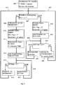
- the block diagram in Figure 1 shows a transmitter unit 1, which supplies one or more receiver units (e.g. 2, 3) wirelessly with energy via one or more coupling factors (e.g. k, k ').
- 1 comprises a large signal VCO 101 which is supplied with the necessary operating voltage from a controlled power source 102.
- 102 is advantageously designed as a controlled and / or regulated switched-mode power supply (SMPS) or linear power supply.
- SMPS switched-mode power supply
- large signal VCO here stands for an oscillator, the active element 104 of which essentially operates in switching mode, but is alternatively also designed as a linear amplifier. Half and full bridge amplifiers are used for this.
- the inverting amplifier 104 drives a resonant circuit, e.g. E.g. a series resonant circuit, consisting of the capacitance C1 and the primary coil L1 of the wireless transmission path.
- a resonant circuit e.g. E.g. a series resonant circuit, consisting of the capacitance C1 and the primary coil L1 of the wireless transmission path.
- One or more reactive elements are controlled in their value by a current or a voltage in order to control the frequency of the oscillator.
- the frequency control advantageously comprises at least one coupling switch which couples at least one inductance or at least one capacitance to the remaining resonant circuit over a variable coupling interval that is less than or equal to one resonant circuit period (not shown in FIG Figure 1 ).
- An inverter 103 closes a feedback loop on the input of 104 and ensures a continuous current or voltage oscillation in the resonant circuit (positive feedback).
- the large-signal VCO is equipped with a parallel push-pull stage which drives a parallel resonant circuit composed of L1 and C1 (not shown in FIG Figure 1 ).
- the descriptions of all the following properties of the transmitter unit are identical for the large-signal VCO with a series resonant circuit and the large-signal VCO with a parallel resonant circuit.
- a resonant circuit signal (output signal fist from 103) is compared in a phase comparator 105 with a desired value (fsoll).
- fsoll is generated in a frequency synthesizer 106 by means of a reference frequency (fref).
- 106 essentially corresponds to a programmable frequency divider, the divider value of which remains stored as a variable in a register within 106.
- the output signal from 105 is filtered by means of a loop filter 107 and then sent to the adjustable capacitance C1 as a control variable. If 101 does not swing to fsoll, 105 generates an error signal at the output which, after filtering with 107 C1, readjusts until fist becomes equal to fsoll.
- 1 emits electromagnetic energy, the frequency of which is regulated to fsoll.
- Any kind of frequency detuning such as For example, component tolerances, aging of the components or changes in a coupled load are corrected within a few oscillating circuit periods.
- An overcoupling detector (OC1) 108 essentially detects a supercritically coupled energy transmission path. This essentially corresponds to the simplified condition k ⁇ Qsec> 1, where Qsec corresponds to the quality of a coupled receiver unit and k to the coupling factor of the coupling path between the transmitter and receiver unit. In the following description, the product k ⁇ Qsec is referred to as energy coupling or, for short, coupling.
- the power or energy received in the receiver unit depends on the square of the coupling. If several receiver units are coupled to 1, the sum of all received powers of all receiver units defines how much power 1 radiates as a minimum. If 1 emits more power than the sum of all received powers of all receiver units, then the difference corresponds to the power that is lost via the stray field.
- the individual partial couplings k ⁇ Qs and k ' ⁇ Qp thus characterize the power or energy transmission of the partial transmission links.
- the notation k ⁇ Qsec summarizes all partial transmission links from several receiver units and is used below as a resultant reaction to 1 for determining the coupling.
- 109 analyzes the period and / or frequency of the oscillator and signals the overcoupling operation to the function controller 109 via the output signal OCT as soon as more than one common pole appears in the resonance mechanism.
- 109 changes, in response to the OCT signal, the oscillator operation via 102 and / or 106. This includes reducing or suspending the emitted field by reducing and / or switching off the operating voltage of the oscillator in 102. Alternatively, or in combination of these measures, the frequency of the oscillator changed via 106. In doing so, 109 changes the divisor variable in 106. This changes the Coupling properties (coupling factor k) of the transmission path or reduces or prevents the transmission of energy. In this way it is guaranteed that essentially only power is emitted as long as the energy transmission path is not operating in the supercritically coupled operating state.
- the supply voltage of 104 is controlled in such a way that the emitted power is as great as it is required in one or more receiver units in order to supply one or more RL with the necessary power.
- the supply voltage from 104 is responsive to FSKLdata via 109 and 102 either in the amplitude changed or sampled or alternatively controlled as a combination of the two.
- FSKLdata contain data which correspond to a control difference between a reference value and an output value determined by the RL. This is determined in 2 and / or 3 and transmitted to 1 wirelessly. This is done, for example, via an additional connection such as WLAN, Bluetooth, Zigbee or as in Fig.1 shown via modulation of the field emitted by 1. Either load modulation or frequency modulation is used for this.
- the data demodulator 111 detects phase adjustment values in accordance with FSKLdata and uses them to generate the messages sent by 2 and / or 3. These messages are transmitted in time division multiplex.
- the divider variable in 106 is sequentially changed from the constant reference frequency fref in such a way that a predetermined frequency spectrum results in fsoll.
- This predetermined frequency spectrum includes e.g. a discrete frequency, an approximate rectangle or a Sin (x) / x etc.
- these specified spectra have zeros or areas in which no power is emitted.
- 106 does not divide any divider values of fref which result in these frequency zeros in fsoll. In this way, any frequency bands can also be generated with any precision relative to fref in the emitted field.
- the power source 102 is modulated in amplitude with a bit sequence continuously or temporarily in accordance with the data Tdata via a further input.
- Tdata are carried to 106 (dashed connection).
- 106 changes the divider value continuously or temporarily in a range around the value specified by 109 with a bit sequence in Tdata. This corresponds to frequency shift keying (FSK) and thus modulates the emitted field in frequency based on Tdata.
- the data stream Tdata is generated in 109 and processed in 109, 102 or 106 such that it corresponds to a Manchester code or a differential Manchester code. Alternatively, this code is implemented as unipolar.
- Tdata in 102 or 106 is ignored if Tdata is not sent.
- a datasend signal is used which takes into account or ignores Tdata in 102 or 106 (not shown in Figure 1 ).
- Figure 1 further shows a receiver unit 2 with a series resonant circuit and a further receiver unit 3 with a parallel resonant circuit, the inductances L2s and L2p of which are coupled to the transmitter unit 1 by inductive coupling.
- the number of two receiver units is arbitrary and shows a power transmission from one transmitter unit to at least one receiver unit. It is also possible whether a receiver unit is used for coupling by means of a series or parallel resonant circuit.
- the load control 200 in FIG. 2 and 300 in FIG. 3 rectify the received AC voltage, filter it and convert it in order to drive at least one RL each.
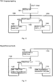
- FIG. 2a shows a block diagram of the receiver unit 2 with the receiving oscillating circuit L2s and C2s.
- the rectifier 203 rectifies the two High frequency half waves equal.
- a coupling switch OCSW couples the rectified AC voltage to a step-up converter 201, consisting of the inductance Lup, switch SWup, diode Dup and capacitor CL, which drives the load resistor RL.
- the diode Df is the freewheeling diode when the OCSW opens and current is still flowing in Lup.
- An overcoupling detector OCdet essentially detects a supercritically coupled energy transmission path. OCdet analyzes the period and / or the frequency of the received alternating voltage using a reference frequency OCfref and signals the overcoupling operation to the controller 202 via the output signal OCL.Similar to 108 in the transmitter unit, OCL changes its state as soon as more than one common pole appears in the resonance mechanism. In response to the OCL signal, 202 opens switch OCSW, which maximizes the effective resistance RL 'at output 203. This minimizes Qs in 2 and minimizes or eliminates the energy transfer. In this way it is guaranteed that essentially only power is received and transmitted to RL as long as the energy transmission path is not operating in the supercritically coupled operating state.
- 201 reduces the pulse width signal PWM and thus generates a shorter control interval in SWup.
- the effective resistance RL 'at output 203 increases. This reduces Qs and results in a smaller coupling of the energy transmission path. In this way it is guaranteed that the energy transmission path always remains below the supercritical coupling state.
- At least part of one or more RL is changed in order to control the coupling (see dashed line in Figure 2a ).
- a main load is advantageously controlled if several partial loads determine an entire RL.
- 202 controls an operating voltage and / or the clock frequency of at least one Processor to change its load.
- Such a processor can be part of a multimedia or any computer unit such as e.g. For example graphic processor (GPU), arithmetic processor, etc.
- 202 controls the voltage or the current of a display background lighting by means of LEDs, or 202 controls the basic brightness or contrast of an OLED display (not shown in FIG Figure 2a ). These displays are part of cell phones, tablets, laptops, glasses, wristband electronics or TVs. Further, 202 controls the voltage or current to charge batteries or drive motors.
- 202 regulates the emitted power in the transmitter unit via FSKLdata and or 202 regulates the output voltage at RL via 201.
- 202 measures the output voltage or output current via or through RL and compares the measured value with a reference value.
- the resulting system deviation value is coupled to SWm together with other data as a serial data stream FSKLdata.
- the data stream FSKLdata advantageously corresponds to a Manchester code or differential Manchester code and is alternatively implemented as a unipolar. Since the power regulation or output voltage regulation via RL in combination with the data transmission by means of FSKLdata in 1 takes place more slowly than the regulation in 201, 201 regulates the fast load changes and 1 regulates the slow load changes.
- Figure 2b shows the secondary quality as a function of the load resistance RL 'of the receiver unit 2 acting on the series resonant circuit (L2s, C2s). Values of 12.5 ⁇ H for L2s and a frequency of 125kHz are taken into account as an example. The smaller RL ', the larger Qs and the better can be compensate for small coupling factors (k). It is clear that the frequency and value information can be changed as required in the explanations.
- FIG. 3a shows a block diagram of the receiver unit 3 with the receiving oscillating circuit L2p and C2p.
- the rectifier 303 rectifies the two high-frequency half-waves.
- a coupling switch OCSW couples the rectified AC voltage to a buck converter 301, consisting of the inductance Ldn, switch SWdn, diode Ddn and capacitor CL, which drives the load resistor RL.
- the inductance Lp and the capacitance Cp filter the rectified voltage at the output of 303.
- An overcoupling detector OCdet essentially detects a supercritically coupled energy transmission path. OCdet analyzes the period and / or the frequency of the received alternating voltage using a reference frequency OCfref and signals the overcoupling operation to the controller 302 via the output signal OCL. Similar to 108 in the transmitter unit, OCL changes its state as soon as more than one pole is established in the resonance mechanism. In response to the OCL signal, the two switches OCSW close 302, which minimizes the effective resistance RL 'on the parallel resonant circuit L2p, C2p. This minimizes Qp in FIG. 3 and minimizes or eliminates the transfer of energy. In this way it is guaranteed that essentially only power is received and transmitted to RL as long as the energy transmission path is not operating in the supercritically coupled operating state.
- 301 reduces the pulse width signal PWM and thus generates a longer control interval in SWdn. As a result, the effective resistance RL 'at output 303 is reduced. This reduces Qp and results in a smaller coupling of the energy transmission path. In this way it is guaranteed that the energy transmission path always remains below the supercritical coupling state.
- At least part of one or more RL is changed in order to control the coupling (see dashed line in Figure 3a ).
- a main load is advantageously controlled if several partial loads determine an entire RL.
- 302 controls an operating voltage and / or the clock frequency of at least one processor in order to change its load.
- Such a processor can be part of a multimedia or any computer unit such as e.g. For example graphic processor (GPU), arithmetic processor, etc.
- 302 controls the voltage or the current of a display background lighting by means of LEDs, or 302 controls the basic brightness or contrast of an OLED display. These displays are part of cell phones, tablets, laptops, glasses, wristband electronics or TVs. Further, 302 controls voltage or current to charge batteries or drive motors.
- 302 regulates the radiated power in the transmitter unit via FSKLdata and or 302 regulates the output voltage at RL via 301.
- 302 measures the output voltage or output current via or through RL and compares the measured value with a reference value.
- the resulting system deviation value is coupled to SWm together with other data as a serial data stream FSKLdata.
- the data stream FSKLdata advantageously corresponds to a Manchester code or differential Manchester code and is alternatively implemented as a unipolar. Since the power regulation or output voltage regulation via RL in combination with the data transmission by means of FSKLdata in 1 takes place more slowly than the regulation in 301, 301 regulates the fast load changes and 1 regulates the slow load changes.
- the output signals from 109 which 102 and / or 106 depending on OCT in the transmitting unit 1 of the Figure 1 control, react with a time delay compared to the OCSW output signals of receiver units 2 and 3 (see Figures 2a and 3a ), if the wireless energy transmission link operates in the supercritically coupled state.
- Electrical energy advantageously remains in L1 and C1 and consequently in the radiated field. As a result, the wireless energy transmission path can immediately transmit power again to receiver units (e.g. 2 and / or 3) as soon as one or more couple with 1 again.
- Figure 3b shows the secondary quality as a function of the load resistance RL 'of the receiver unit 3 acting on the parallel resonant circuit (L2p, C2p). Values of 12.5 ⁇ H for L2p and a frequency of 125kHz are taken into account as an example. The larger RL ', the larger Qp and the easier it is to compensate for small coupling factors (k).
- the rectified AC voltage Vr is additionally coupled to 202 and 302 in order to generate all partial operating voltages that are required for operation in FIGS.
- 202 and 302 include voltage stabilization circuits.
- a maximum voltage of Vr is detected in 202 and 302 (overvoltage protection), and as soon as the maximum voltage value is exceeded, the coupling is reduced or minimized via the Qsec. This is done as described above using 201, 202, 301, 302 and / or by controlling RL, but in the opposite direction as described above, so that the coupling is reduced. In this way 2 and 3 are protected from overvoltage.
- 202 and 302 include analog-to-digital converters.
- Vr or a frequency reference e.g. For example, OCfref is used as a clock generator in 202 and 302.
- the frequency reference e.g., OCfref is generated by a crystal oscillator.
- single or multiple clock frequencies are derived from the timing of Vr in order to process input signals in synchronism with the received electromagnetic field.
- FIG. 11 shows an embodiment of the control method of a sequential coupling control of the receiver units 2 and 3 as shown in FIGS Figures 2a, 2b and 3a, 3b are described above.
- the initial condition is no prior coupling between 1 and 2 and / or 3.
- An increasing coupling factor (k) is also assumed, a situation that often occurs in practice as soon as 1 and 2 and / or 3 approach.
- the method described applies generally without any further restriction with regard to FIGS. 2 and 3 and is based on the description of FIGS Figures 2a, 2b , 3a and 3b referenced.
- step 400 this ensures the greatest range, e.g. E.g. when 1 and 2 and / or 3 are approaching.
- step 401 it is detected whether overcoupling is occurring, signaled here with a logic "1" via the signal OCL. If OCL does not indicate any cross-coupling (e.g. OCL with logical "0"), 2 or 3 can continue to operate with maximum quality (output path "No").
- status registers are written e.g. E.g. the OCL flag, which is part of FSKLdata and 1 notifies the coupling status of 2 and / or 3.
- the communication of new FSKLdata is enabled by means of SendENA with a logical "1".
- the time constant (LinkTimer) is set in 403 and is decremented in loops 404, 405 and 408 as long as it has not expired.
- a predefined "Constant A” is loaded into the LinkTimer and continuously decremented. If the counter reading in the LinkTimer becomes zero, the pulse duty factor in the PWM control signal of 201, 301 and / or RL is increased 406 in such a way that the quality Qsec increases. As a result, the coupling increases.
- the feedback path 407 initiates a renewed detection of the coupling with 401. This loop ensures that the wireless energy transmission path can always be operated with the most critical coupling possible or that it approaches this value. If the signal OCL is detected with a logic “1” in 401 (output “YES”), in 409 RL is decoupled from 1 via OCSW in 2 and / or 3. As a result, the coupling between 1 and 2 and / or 3 is minimal.
- step 410 status registers are written e.g. E.g. the OCL flag, which is part of the FSKLdata and 1 notifies the coupling status of 2 and / or 3.
- the communication of new FSKLdata is interrupted by means of SendENA with a logic "0".
- FSKLdata is transmitted in a different frequency band (such as e.g. Bluetooth, WLAN, Zigbee or NFC) and the control by means of SendENA is not implemented.
- the pulse duty factor in the PWM control signal from 201, 301 and / or RL is controlled in such a way that the quality Qsec is reduced the next time 1 and 2 and / or 3 are recoupled.
- the time constant (OCTimer) is set in 412 and is decremented in loops 413, 415 and 416 as long as it has not expired.
- a predefined "KonstanteB" is used in the OCTimer loaded and continuously decremented. If the count in the OCTimer goes to zero, 414 couples RL in 2 and / or 3 to 1 by means of OCSW. As a result, RL is again coupled to 1, the coupling being smaller between 1 and 2 and / or 3.
- the feedback path 417 initiates renewed detection of the overcoupling with 401. This loop ensures that the coupling always moves away from the supercritical state and the wireless energy transmission path never gets stuck in the overcoupling state.
- the two feedback paths 407 and 417 together maximize the coupling of the wireless energy transmission paths between 1 and 2 and / or 3.
- the stray field is advantageously minimized, which means lower emissions and fewer interference fields.
- Figure 4 shows the coupling control or coupling optimization in the event that the output voltage VOUT is not reached via RL. If the maximum VOUT is exceeded, the pulse duty factor in PWM is reduced in 2 and / or 3 regardless of the coupling control. Alternatively or as a combination, RL in 2 and / or 3 is controlled in such a way that the maximum VOUT is not exceeded.
- 202 and 302 contain VOUT regulations as they are used in common SMPS. These regulations essentially regulate the fast, small load changes in 2 and / or 3. 1 takes over the sluggish regulation by means of 102 via FSKLdata and 109.
- the flow control of the steps in Figure 4 is processed by an internal cycle of 202 and 302.
- this clock pulse is synchronous with the time profile of Vr and consequently synchronous with the received electromagnetic field.
- the steps in FIG Figure 4 processed by an internal clock of 202 and 302, which is not synchronous with the electromagnetic field (e.g. OCfref).
- FIG Figure 5a Another embodiment of the current invention is shown in FIG Figure 5a an oscillating circuit L0, C01 and C02, which at the same resonance frequency in a first mode, hereinafter referred to as series mode, operates in series resonance and in a second mode, hereinafter referred to as parallel mode, operates in parallel resonance.
- C01 and C02 are connected in series with L0 via the full-wave rectifier 501.
- L0 corresponding to L2s, L2p in Figure 1 receives the electromagnetic field emitted by the transmitter unit 1.
- the mode switch SWS / P2 which contains two switches, one each parallel to the grounded diodes of 501.
- the positive output of 501 is coupled via a series filter inductance Lf to the charging capacitor CL and to the load resistor RL.
- a further full-wave rectifier 503 is connected in parallel with L0, the positive output of which is coupled to CL and RL via a further mode switch SWS / P1.
- the control signal S / P from SWS / P1 and SWS / P2 is generated in the S / P controller 502.
- 502 is largely identical in terms of its functions and includes processing steps similar to 202 in FIG Figure 2a and 302 in Figure 3a . This mainly affects the signals VOUT, OCL and FSKLdata. This also applies to the internal clock, the internal supply and the control of RL (not shown here). The internal supply and the clock derivation from the received magnetic field takes place via VrS and / or VrP.
- the output of 503 is also coupled via a tap from Lf to CL.
- Vr is needed either from 501 or from 503 of Lf.
- additional switches SWOV and a diode DOV are implemented in the current path from Lf to CL.
- SWOV and DOV act together as a protection circuit in a protection mode.
- OCdet and the FSKLdata modulation using Cm and SWm are implemented in the same way as in 202 and / or 302.
- the diodes of 501 rectify the resonance voltage and conduct it to the load RL via Lf, which as a filter inductance approximates sinusoidal current flow in the resonant circuit load.
- Lf which as a filter inductance approximates sinusoidal current flow in the resonant circuit load.
- SWS / P1 and SWS / P2 can be viewed as non-existent in series mode.
- Symmetry condition should be complied with as far as possible in order to distribute the resonant circuit resonance voltage evenly over C01 and C02.
- the midpoint of SWS / P2 thus becomes an alternating voltage zero point and 501 interrupts the flow of current to Lf, since the voltages over 501 reach a maximum of half the voltage over L0.
- Figure 5c the currents of the positive half-wave (solid arrows) and the currents of the negative half-wave (dashed arrows) are shown.
- L0, C01 and C02 act as a current source.
- the diodes of 503 rectify the resonance voltage and direct it to the load RL.
- 501 and Lf can be considered non-existent in parallel mode. If Lf still carries energy from a previous series mode, 501 conducts until Lf has discharged.
- a signal is present at output S / P of 502 (e.g. "1" level), which leaves SWS / P1 and SWS / P2 closed, which corresponds to the parallel mode.
- S / P of 502 e.g. "1" level
- the wireless energy transmission path is essentially always in resonance coupling.
- one or more receiver loads (RLs) are actually coupled to the transmitter unit and guarantee optimal adaptation.
- SWS / P1 is in the ground lead of 503 and the positive output of 503 is directly connected to Lf or a tap thereof.
- Lf is located between the ground and the center of SWS / P2 instead of between the midpoint SWOV and CL.
- CL is connected directly to the midpoint of SWOV.
- Lf is located between the ground and the center of SWS / P2 instead of between the midpoint SWOV and CL.
- the SWS / P1 is located in the ground lead of 503 and the positive output of 503 is connected directly to CL.
- SWS / P1 is not connected directly to ground, but is connected to a tap from Lf.
- L0 has a center tap and 503 is implemented as a full-wave rectifier, see FIG Figure 6a . Thanks to the center tap of L0, two diodes can be saved in 603.
- the series / parallel mode switching is identical to Figure 5a about S / P. The same applies to the series mode as in Figures 5a and 5b .
- the parallel mode only generates half of the output voltage at the output of 603 compared to the circuit after Figures 5a and 5c . So that 601 is safely decoupled, the output of 603 is coupled to CL via a tap from Lf. This transforms the output voltage of 603 to the output of 601 and blocks its upper two diodes. This leaves only the current path from the tap from Lf to RL as it is in Figure 6b is shown.
- the rectification voltage is coupled to 602 via Vr for both series and parallel modes.
- the diodes in 501, 503, 601 and 603 are at least partially implemented as synchronous rectifiers.
- SWS / P2 and SWOV are then part of 501 and 601.
- the synchronous rectifiers can then be used as normal synchronous rectifiers at a level in S / P (e.g. "0").
- S / P e.g. "1" level
- at least part of the synchronous rectifier is imperatively conductive, ie two diodes are necessarily short-circuited by SWS / P2.
- Figure 5e shows the quality characteristics as a function of RL of the circuit of the Figure 5a at the same frequency and L0 as in the Figures 2b and 3b .
- the circuit With low RL values (see Qs area), the circuit delivers high quality values in series mode.
- the circuit At the RL value, at which the Q values in series and parallel mode are equal, the circuit reaches its lowest maximum quality value Qsec.
- the circuit delivers high quality values in parallel mode (see Qp area).
- VOUT is regulated via S / P without considering the control of 1 via FSKLdata.
- VOUT is regulated via S / P and FSKLdata, ie taking into account the control of 1 via FSKLdata.
- S / P takes over the quick adjustment, 102 in Figure 1 via 109 and by means of FSKLdata the slow adjustment.
- VOUT is regulated via S / P in such a way that 502 and / or 602 receives FSKLdata from at least one other coupled receiver unit (e.g. 2 and / or 3) and sends its own output signals S / P and / or FSKLdata are dependent on the previously received FSKLdata from at least one other coupled receiver unit (e.g. 2 and / or 3).
- S / P and / or FSKLdata output signals react in their values (PWM duty cycle and / or serially transmitted data) to previously received FSKLdata from at least one other coupled receiver unit (e.g. 2 and / or 3).
- Figure 7 shows a state machine which describes the timing of parts within 502 and 602, respectively.
- the Figure 8 State 702: coupling optimization
- the Figure 9 State 701: coupling limitation
- Figure 10 State 703: output regulation
- the output voltage is written to a desired setpoint value Vsoll.
- the output current is regulated to a desired setpoint value Isoll.
- the current is measured through one or more RLs and fed back to 502 and / or 602.
- the timers described for the Figures 8-11 are controlled by a clock or several clocks with the following properties: At least one clock is either synchronous with at least one of the signals Vrs, Vrp and Vr or at least one clock is synchronous with OCfref.
- one or more clock signals can be varied in frequency in further exemplary embodiments of the current invention.
- Pseudorandom generators are used to divide clock signals from Vrs, Vrp, Vr or OCfref, which have quasi-random properties.
- the spectral mixing products and interferences of the control loops described below are blurred. This minimizes the maxima of the interference radiation of the electromagnetic radiation due to load changes and / or control or regulating behavior.
- S / P is set to series mode in the case of a minimum RL initial value (e.g. incandescent lamp), or S / P is set to parallel mode in the case of a maximum RL initial value (e.g. LED) .
- a constant Konst1 is loaded into the OptiTimer.
- Step 802 stores the current output voltage VOUT in the variable Vcompare.
- 803 checks whether OptiTimer has already expired or whether OptiTimer has reached a defined end value (e.g. counter reading "0").
- Const1 defines the loop time of 702, which is minimal at half a period of the received electromagnetic field, provided it is synchronized via Vrs, Vrp or Vr.
- the loop time of 702 is synchronized by OCfref and is minimally less than half a period of the received electromagnetic field. Ie series / parallel mode switch back and forth faster than in the half-period cycle of the received electromagnetic field.
- the OCL flag which is a message part of FSKLdata
- the OCTimer is loaded with a constant Konst3.
- 912 again compares how 904 the OCTimer to its final value and decrements OCTimer via 914 and 915 to 912 refers to 913.
- the reset SWOV RL then couples again with 1.
- OCL is reset again in 916 and the state machine is set to 702 again. It is obvious that 701 can be simplified further or the OCTimer loops can be combined can be.
- Konst2 and Konst3 are the same or different and are further such that OCTimer does not reach its final value for at least half a period of the received electromagnetic field.
- state 703 is active. In this, S / P changes its state to 1001. If RL is in the range Qs or Qp, the quality Qsec is immediately reduced (see curve in Figure 5e ). Qsec changes e.g. E.g. from A to B or from z. Example C to D and consequently the smaller coupling reduces the output variable VOUT. 1002 then compares again whether VOUT is greater than Vsoll. If VOUT is less than Vsoll, OVS is reset in 1005 and the loop at input 1002 is closed via 1006.
- the protection mode is active.
- RL decouples from 1 and Qsec becomes minimal.
- the power or energy transferred from 1 to 2 or 3 is advantageously also minimal. This reduces VOUT.
- the feedback 1004 causes a dwell within 703 until VOUT is less than Vsoll. If this is the case, state 703 changes to 702. If overcoupling occurs in 703, 703 changes to 701. In this way, operation with supercritical coupling is always avoided.
- the wireless energy transmission path is continuously optimized for maximum critical coupling by means of series-parallel mode (S / P signal) and with continuous overcoupling protection (S / P and OVS signals) or follows the curve in for each RL value Figure 5e .
- the control by means of FSKLdata which transfers the control difference, or, if several RLs are available, the sum of a control difference, is transferred to 1 Figure 11 shown.
- 1101 loads a constant Konst4 into the FSKLTimer.
- 1102 detects whether FSKLTimer has reached a defined end value (e.g. counter reading "0"). If this final value has not yet been reached, 1105 decrements the FSKLTimer and inserts a new current system deviation value (Vsoll-VOUT) into a loop array.
- the feedback 1106 effects this loop cycle until the FSKLTimer reaches its end value.
- 1103 calculates an average system deviation value, which is transferred to 1 within FSKLdata.
- the calculation of the averaged system deviation value within 1103 includes, in one embodiment, dividing the sum of all system deviation values in the loop array by Const4.
- the control deviation loop operates continuously. As described, 1 controls the output power and consequently also the receivable power in 2 and / or 3. If rather little power is received, the state machine pauses according to Figure 7 long in 702. This has the effect of increasing the coupling and the radiated transmit power, since FSKLdata controls the radiated power. If VOUT reaches Vsoll, 702 changes to 703. 703 does not optimize the coupling, which means that the steady-state accuracy (control difference equal to zero) and optimal coupling do not always converge. For this reason, in an exemplary embodiment of the current invention, a correction value is included in 1103, which takes into account the dwell time or percentage dwell time or the ratio of the states 702 and 703. Alternatively, in a further exemplary embodiment, the dwell time or percentage dwell time is also included in 701 or weighted accordingly.
- the constants Konst1 - Konst4 can be used to optimize parameters such as control characteristics, response time, efficiency, etc. for different dynamic loads RLs depending on the desired requirements.
- switch SWOV is in series between 501 and Lf in Figure 5a or in series between 601 and Lf in Figure 6a placed.
- the protection mode is then implemented by means of series mode in the S / P signal and open SWOV by means of the OVS signal (not shown). In this way, smaller losses are advantageously achieved in protection mode, since no current flows.
- FIGS Figures 5a and 6a additionally combined with a buck converter or boost converter and / or with a combined buck converter-boost converter (see Figure 12 ).
- the electromagnetic field lines emitted by 1 are generated by L0 and the series parallel receiver circuit according to Figure 5a receive. 1203 corresponds to 503, 1201 corresponds to 501 and the SWOV switches are not implemented in parallel to the rectifier diodes, but are part of the following buck and boost converter 1205.
- the other circuit parts are unchanged Figure 5a .
- the output of filters Lf, Cf feeds 1205, where SWOV corresponds to the buck converter and Df corresponds to its freewheeling diode.
- SWup corresponds to the step-up converter switch and Dup its clamping diode.
- the exit controller 1204 communicates with the S / P controller over the bus.
- the signals VOUT, internal clock signals (e.g. OCfref or clocks derived from VrP or VrS), OVS and S / P are transmitted in analog or digital form between 1202 and 1204.
- 1205 transforms RL by means of the corresponding control signals Dn and / or Up.
- the circuits in the Figures 5a and 6a have the disadvantage that the quality cannot be controlled arbitrarily over the entire RL range (see curve in Figure 5e ). For example, for the RL range from 2.5 to 40 ohms, a quality Qsec less than 4 always results.
- 1202 and 1204 jointly optimize the behavior described above and maximize a constant Qsec over a wide RL range.
- the state machine after Figure 7 still applies, 701, 702 and 703 have been modified.
- the quality is optimized for the maximum critical coupling possible via S / P and 1205 (state 702).
- the fast output control is made via S / P and / or 1205 or VOUT is limited (state 703).
- the slower regulation takes place via FSKLdata to 1. This advantageously results in the highest possible coupling, which is always smaller than supercritical and results in the smallest possible energy emission of 1. In fact, on average, ideally only as much energy is emitted as is required at RL. In this way, this approximates a wire connection between 1 and RL as closely as possible.
- RL is calculated using an additional RL current measurement in 1204 (not shown in FIG Figure 12 ). Since L0 represents a design parameter, L0 or point X is stored in memory in 1204 and / or 1202. 1204 controls the S / P signal via the bus and at the same time defines the operating mode of 1205.
- Im Series mode works 1205 with the highest possible boost converter transformation. If supercritical coupling is detected by OCL, then 701 first of all reduces the transformation in 1205 and only secondly the mode is changed by S / P. In parallel mode, 1205 works with the highest possible buck converter transformation. If supercritical coupling is detected by OCL, then 701 firstly reduces the transformation in 1205 and only secondly S / P is changed.
- the transformation in 701 (not shown) is not only decremented in value, but also significantly reduced (e.g. halved).
- the transformation from 1205 is only slowly increased (for example, incremented). In this way, any cross-coupling is always quickly removed and the system then slowly approaches the maximum possible Qsec again.
- 1202 and 1204 are implemented as combined subroutines of a software control in a microcontroller.
- FSKLdata is not modulated by means of frequency keying (Cm, SWm), but rather by briefly switching the S / P signal through FSKLdata or a serial bit sequence that reacts to FSKLdata.
- This modulates the coupling as a function of FSKLdata and corresponds to a load modulation which is detected in FIG.
- a receiver detects FSKLdata messages from other receivers. The coupling via Qsec is modified by other receivers in response to FSKLdata received from other receivers.
- this behavior is initiated by an authorization. This authorization takes place via a different message channel (e.g. WLAN, Bluetooth or NFC).
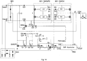
- Figure 14 shows a detailed implementation according to Figure 6a whose switch SWS / P1 is now not in the positive current path to Lf, but is implemented from ground to the center tap of L0. All components of Figure 6a can be found under the same reference in Figure 14 Find.
- One half of 601 can advantageously be combined with SWS / P2 and the other half of 601 with SWOV.
- the components A1 - A4, R1 - R4 and the gate resistors correspond to a standard circuit of commercially available synchronous rectifier driver ICs such as. E.g. TEA1761 and TEA1791.
- the operating voltage supply for these ICs is in Figure 14 Not shown.
- the output of synchronous rectifier 601 / SWOV drives RL through Lf, DOV and CL.
- Caux1 and Caux2 branch off a small amount of resonant circuit energy and generate a small stable negative voltage (approx. -1.4V) in Vaux, which is coupled to the source of Q5.
- S / P and OVS are "0"
- Q5, Q4, Q2, SWS / P1 and Q6 are not conductive.
- all switches in 601 / SWS / P2 and 601 / SWOV work as normal synchronous rectifiers. This corresponds to the series mode.
- Q3 enables zero voltage switching (ZVS) in SWS / P1 when switching from series to parallel mode.
- Q3 only blocks if the tap from L0 is not more negative than approx. -0.7V. This occurs once per oscillation half-wave in the oscillating circuit L0, C0.
- 601 / SWOV is controlled. If OVS is "0", Q6 blocks and 601 / SWOV works as a synchronous rectifier. If OVS is "1", Q6 leads. B3 and B4 generate a voltage drop via R3 and R4, which makes the switch SWOV mandatory. S / P switches to parallel mode so that the circuit is in protection mode. In this case it flows Current rectified in 603 no longer through DOV in RL, but via switches SWOV and SWS / P2 to ground and finally via SWS / P2 back to L0.
- the gate resistances of the MOSFET transistors in Figure 14 are low-resistance and prevent oscillations in the gate control.
- the diodes D2 - D5 are anti-saturation diodes and accelerate the switching behavior of the bipolar transistors.
- DOV is implemented as an active switch. This switch is then controlled by OVS or by a synchronous rectifier driver.
- Cm is coupled to C02 by SWm if FSKLdata goes to "1".
- Q7 blocks via D6. If FSKLdata is "0", Q7 conducts until there is no longer any gate voltage at SWm.
- 603 is implemented as a synchronous rectifier according to 601 and its synchronous rectifier drivers A3 and A4.
- FF1 is not clocked via the quasi voltage zero point from the center tap of L0, but by a peak value detector of Vr (not shown in FIG Figure 14 ).
- Vr peak value detector
- the concepts described in this invention can be used in any multimedia device such as tablet, mobile phone, TV, portable player, camera, glasses, wristwatch or wristband control unit with display, in every mobile power-operated tool, in all electrical household appliances and in electronically equipped clothing (wearable electronics ) can be used.
- the concepts described in this invention are not only suitable for consumer devices, but also for devices in medical technology, including medical implants, in mechanical engineering, in agriculture, in mining or on production platforms, in aerospace and seafaring Electromobility and for automobile and motor vehicle applications.
Landscapes
- Engineering & Computer Science (AREA)
- Computer Networks & Wireless Communication (AREA)
- Power Engineering (AREA)
- Near-Field Transmission Systems (AREA)
- Transmitters (AREA)
- Circuits Of Receivers In General (AREA)
- Dc-Dc Converters (AREA)
Claims (13)
- Procédé de couplage d'une énergie sans fil à une charge (RL), comprenant :la réception d'énergie sans fil dans un récepteur au moyen d'un circuit résonnant (L0, C01, C02) qui est formé par au moins un condensateur (C01, C02) et au moins une bobine (L0),la commutation du circuit résonant (L0, C01, C02) par un premier commutateur (SWS/P2) entre un premier mode et un second mode, dans lequel dans le premier mode le circuit résonant fonctionne en résonance parallèle et dans le second mode le circuit résonant fonctionne en résonance série et caractérisé par;le redressement pleine onde par un premier redresseur (501, 601) d'une tension alternative générée par l'énergie sans fil reçue dans le second mode du circuit résonnant et alimentant la charge (RL), dans lequel le premier commutateur (SWS/P2) comprend deux transistors connectés en parallèle à deux diodes du premier redresseur (501, 601) de telle sorte qu'un transistor ponte à chaque fois une diode et que le milieu du circuit des deux diodes avec les deux transistors du premier commutateur (SWS/P2) montés en parallèle représente un point zéro de tension alternative du circuit résonnant dans au moins l'un des deux modes, et dans lequel le premier mode est actif lorsque le premier commutateur (SWS/P2) est fermé, et dans lequel les deux transistors du premier commutateur (SWS/P2) dans le deuxième mode réalisent au moins partiellement le redressement pleine onde,le redressement par un second redresseur (503, 603) d'une tension alternative générée par l'énergie sans fil reçue dans le premier mode du circuit résonnant parallèle,le couplage de la tension alternative redressée du second redresseur à la charge par un second commutateur (SWS/P1) dans le premier mode,le découplage de la tension alternative redressée du second redresseur de la charge par le second commutateur (SWS/P1) dans le second mode, etla génération des signaux de commande des premier et second commutateurs.
- Procédé selon la revendication 1, dans lequel les transistors du premier commutateur et leurs diodes connectées en parallèle sont chacun combinés dans un MOSFET, et le circuit résonnant (L0, C01, C02) sort la puissance sans fil reçue vers la charge (RL) dans les premier et second modes.
- Procédé selon la revendication 1, dans lequel la commutation du circuit résonant (L0, C01, C02) entre le premier et le second mode :a1) répond à la charge (RL) ; oua2) répond à une tension aux bornes de la charge (RL), oua3) répond à un courant à travers la charge (RL), oua4) répond à un surcouplage détecté de la liaison de transmission d'énergie sans fil sur laquelle l'énergie sans fil est reçue.
- Procédé selon la revendication 1, dans lequel le circuit résonnant a la même fréquence de résonance dans les premier et second modes, et/ou dans lequel au moins un condensateur (C01, C02) et au moins une bobine (L0) forment
le circuit résonnant à la fois dans le premier mode et dans le second mode. - Procédé selon la revendication 1, dans lequel le redressement pleine onde dans le deuxième mode comprend en outre:
le redressement synchrone par les deux transistors du premier commutateur (SWS/P2) de la tension alternative générée par l'énergie sans fil reçue dans le second mode du circuit résonnant. - Procédé selon la revendication 1, dans lequel le redressement du circuit résonant parallèle dans le premier mode comprend en outre:
le redressement pleine onde par le deuxième redresseur (503, 603) de la tension alternative générée par l'énergie sans fil reçue dans le premier mode du circuit résonant. - Un récepteur pour recevoir de l'énergie sans fil, comprenant:un circuit résonnant (L0, C01, C02) pour recevoir de l'énergie sans fil formé par au moins un condensateur (C01, C02) et au moins une bobine (L0),un premier commutateur (SWS/P2) pour commuter le circuit résonnant (L0, C01, C02) entre un premier mode et un second mode, dans lequel dans le premier mode le circuit résonnant fonctionne en résonance parallèle et dans le second mode le circuit résonnant fonctionne en résonance série et caractérisé par ;un premier redresseur (501, 601) pour redresser à double alternance la tension du circuit résonnant dans le second mode pour alimenter une charge (RL), dans lequel le premier commutateur (SWS/P2) comprend deux transistors connectés en parallèle à deux diodes du premier redresseur (501, 601) de telle sorte que, dans chaque cas, un transistor ponte une diode et le centre du circuit des deux diodes avec les deux transistors du premier commutateur (SWS/P2) connectés en parallèle représente un point zéro de tension alternative du circuit résonnant dans au moins l'un des deux modes, et dans lequel le premier mode est actif lorsque le premier commutateur (SWS/P2) est fermé, et dans lequel les deux transistors du premier commutateur (SWS/P2) font partie du redresseur pleine onde dans le second mode, etun deuxième redresseur (503, 603), en parallèle avec au moins une bobine, pour générer une tension de circuit résonnant parallèle redressée, etun second commutateur (SWS/P1) pour coupler la tension de circuit résonnant parallèle redressé à la charge (RL) dans le premier mode, et pour découpler la tension de circuit résonnant parallèle redressé de la charge (RL) dans le second mode, dans lequel un contrôleur génère les signaux de commande des premier et second commutateurs.
- Le récepteur selon la revendication 7, dans lequel les transistors du premier commutateur et leurs diodes connectées en parallèle sont chacun combinés en un MOSFET, et/ou
dans lequel le circuit résonnant (L0, C01, C02) émet une puissance sans fil reçue vers la charge (RL) dans les premier et second modes. - Le récepteur selon la revendication 7, dans lequel la commutation du circuit résonant (L0, C01, C02) entre le premier et le second mode:a1) répond à la charge (RL) ; oua2) répond à une tension aux bornes de la charge (RL), oua3) répond à un courant à travers la charge (RL), oua4) répond à un surcouplage détecté de la liaison de transmission d'énergie sans fil sur laquelle le récepteur reçoit de l'énergie.
- Le récepteur selon la revendication 7, dans lequel le circuit résonnant a la même fréquence de résonance dans les premier et second modes, et/ou dans lequel au moins un condensateur (C01, C02) et au moins une bobine (L0) forment le circuit résonnant à la fois dans le premier mode et dans le second mode.
- Le récepteur selon la revendication 7, dans lequel les deux transistors du premier commutateur (SWS/P2) font partie d'un redresseur synchrone du premier redresseur.
- Le récepteur selon la revendication 7, dans lequel le deuxième redresseur (503, 603) est mis en œuvre comme un redresseur pleine onde (503, 603) ou un redresseur bidirectionnel (603).
- Le récepteur selon la revendication 7, dans lequel le circuit résonnant (L0, C01, C02) forme un circuit résonnant symétrique d'au moins trois composants réactifs et dans lequel deux des trois composants réactifs sont du même type et au moins une partie de la tension de résonance du circuit résonnant symétrique dans au moins l'un des deux modes est distribuée de manière égale aux composants réactifs du même type, et/ou dans lequel le circuit résonant (L0, C01, C02) forme un circuit résonant symétrique d'au moins trois composants réactifs et ces trois composants réactifs forment le circuit résonant à la fois dans le premier mode et dans le second mode.
Priority Applications (1)
| Application Number | Priority Date | Filing Date | Title |
|---|---|---|---|
| EP21000270.5A EP4009485A3 (fr) | 2014-12-29 | 2015-11-30 | Transmission d'énergie électrique sans fil optimisée au niveau de couplage |
Applications Claiming Priority (2)
| Application Number | Priority Date | Filing Date | Title |
|---|---|---|---|
| DE102014019621.6A DE102014019621A1 (de) | 2014-12-29 | 2014-12-29 | Kopplungsoptimierte elektrische drahtlose Energieübertragung |
| EP15003405.6A EP3041112B1 (fr) | 2014-12-29 | 2015-11-30 | Transmission d'energie electrique sans fil a couplage optimise |
Related Parent Applications (2)
| Application Number | Title | Priority Date | Filing Date |
|---|---|---|---|
| EP15003405.6A Division-Into EP3041112B1 (fr) | 2014-12-29 | 2015-11-30 | Transmission d'energie electrique sans fil a couplage optimise |
| EP15003405.6A Division EP3041112B1 (fr) | 2014-12-29 | 2015-11-30 | Transmission d'energie electrique sans fil a couplage optimise |
Related Child Applications (2)
| Application Number | Title | Priority Date | Filing Date |
|---|---|---|---|
| EP21000270.5A Division-Into EP4009485A3 (fr) | 2014-12-29 | 2015-11-30 | Transmission d'énergie électrique sans fil optimisée au niveau de couplage |
| EP21000270.5A Division EP4009485A3 (fr) | 2014-12-29 | 2015-11-30 | Transmission d'énergie électrique sans fil optimisée au niveau de couplage |
Publications (2)
| Publication Number | Publication Date |
|---|---|
| EP3451490A1 EP3451490A1 (fr) | 2019-03-06 |
| EP3451490B1 true EP3451490B1 (fr) | 2021-11-24 |
Family
ID=54783325
Family Applications (3)
| Application Number | Title | Priority Date | Filing Date |
|---|---|---|---|
| EP21000270.5A Pending EP4009485A3 (fr) | 2014-12-29 | 2015-11-30 | Transmission d'énergie électrique sans fil optimisée au niveau de couplage |
| EP15003405.6A Active EP3041112B1 (fr) | 2014-12-29 | 2015-11-30 | Transmission d'energie electrique sans fil a couplage optimise |
| EP18000770.0A Active EP3451490B1 (fr) | 2014-12-29 | 2015-11-30 | Transmission d'énergie électrique sans fil optimisée au niveau d'accouplement |
Family Applications Before (2)
| Application Number | Title | Priority Date | Filing Date |
|---|---|---|---|
| EP21000270.5A Pending EP4009485A3 (fr) | 2014-12-29 | 2015-11-30 | Transmission d'énergie électrique sans fil optimisée au niveau de couplage |
| EP15003405.6A Active EP3041112B1 (fr) | 2014-12-29 | 2015-11-30 | Transmission d'energie electrique sans fil a couplage optimise |
Country Status (3)
| Country | Link |
|---|---|
| US (3) | US10411511B2 (fr) |
| EP (3) | EP4009485A3 (fr) |
| DE (1) | DE102014019621A1 (fr) |
Families Citing this family (14)
| Publication number | Priority date | Publication date | Assignee | Title |
|---|---|---|---|---|
| EP2765701B1 (fr) * | 2013-02-08 | 2020-01-01 | Markus Rehm | Transmission d'énergie électrique sans fil avec couplage à résonance |
| JP6437954B2 (ja) * | 2016-06-02 | 2018-12-12 | パナソニック株式会社 | 無線給電方法 |
| US10879739B2 (en) * | 2017-04-12 | 2020-12-29 | Integrated Device Technology, Inc. | Wireless power transmitter reactive energy control |
| CN108365683B (zh) * | 2018-02-10 | 2021-04-27 | 合肥工业大学 | 一种基于电流源的无线能量传输结构 |
| ES2826433T3 (es) * | 2018-02-19 | 2021-05-18 | Naptilus Tech Lab S L | Aparato sintonizador y rectificador para receptor de transferencia de potencia inalámbrica |
| US12057711B2 (en) * | 2018-02-19 | 2024-08-06 | Naptilus Technology Lab, S.L. | Tuner and rectifier circuit for wireless power receiver |
| US10205381B1 (en) * | 2018-05-10 | 2019-02-12 | Vlt, Inc. | Start-up control in power systems using fixed-ratio power conversion |
| US11296552B2 (en) * | 2018-06-12 | 2022-04-05 | Nanyang Technological University | Transmitter device, wireless power transfer system, and methods of forming the same |
| JP6773257B1 (ja) * | 2019-04-26 | 2020-10-21 | 三菱電機株式会社 | エレベータ |
| JP6729920B1 (ja) * | 2019-08-08 | 2020-07-29 | 株式会社レーザーシステム | 共振装置、電力伝送装置、及び電力伝送方法 |
| US11495995B2 (en) * | 2019-09-23 | 2022-11-08 | Stmicroelectronics Asia Pacific Pte Ltd | Advanced overvoltage protection strategy for wireless power transfer |
| JP6849778B1 (ja) * | 2019-12-05 | 2021-03-31 | パナソニック株式会社 | 無線送電器、および無線受電器 |
| CN116057811B (zh) * | 2020-08-18 | 2024-11-19 | 微芯片技术股份有限公司 | 用于无线功率接收器的装置、无线功率接收器及其操作方法 |
| US12341984B2 (en) * | 2022-12-14 | 2025-06-24 | Qualcomm Incorporated | Truncation error signaling and adaptive dither for lossy bandwidth compression |
Citations (2)
| Publication number | Priority date | Publication date | Assignee | Title |
|---|---|---|---|---|
| US5831348A (en) * | 1996-06-03 | 1998-11-03 | Mitsubishi Denki Kabushiki Kaisha | Secondary circuit device for wireless transmit-receive system and induction coil for wireless transmit-receive system |
| WO2014178345A1 (fr) * | 2013-04-30 | 2014-11-06 | 矢崎総業株式会社 | Système d'alimentation électrique et circuit résonant |
Family Cites Families (24)
| Publication number | Priority date | Publication date | Assignee | Title |
|---|---|---|---|---|
| US8232970B2 (en) * | 2007-01-03 | 2012-07-31 | Apple Inc. | Scan sequence generator |
| JP5340017B2 (ja) * | 2009-04-28 | 2013-11-13 | 三洋電機株式会社 | 電池内蔵機器と充電台 |
| US8390249B2 (en) * | 2009-11-30 | 2013-03-05 | Broadcom Corporation | Battery with integrated wireless power receiver and/or RFID |
| US10693853B2 (en) * | 2010-07-23 | 2020-06-23 | At&T Intellectual Property I, Lp | Method and system for policy enforcement in trusted ad hoc networks |
| KR101750415B1 (ko) * | 2010-12-16 | 2017-06-26 | 삼성전자주식회사 | 정류기를 보호하는 보호기, 상기 보호기를 포함하는 무선전력 수신 장치 |
| JP5677875B2 (ja) * | 2011-03-16 | 2015-02-25 | 日立マクセル株式会社 | 非接触電力伝送システム |
| KR101813011B1 (ko) * | 2011-05-27 | 2017-12-28 | 삼성전자주식회사 | 무선 전력 및 데이터 전송 시스템 |
| JP5840886B2 (ja) * | 2011-07-25 | 2016-01-06 | ソニー株式会社 | 検知装置、受電装置、送電装置、非接触電力伝送システム及び検知方法 |
| US9508487B2 (en) * | 2011-10-21 | 2016-11-29 | Qualcomm Incorporated | Systems and methods for limiting voltage in wireless power receivers |
| KR101304314B1 (ko) * | 2012-01-30 | 2013-09-11 | 전자부품연구원 | 임피던스 매칭이 가능한 무선 전력 송신장치 |
| US9531441B2 (en) * | 2012-02-21 | 2016-12-27 | Lg Innotek Co., Ltd. | Wireless power receiver and method of managing power thereof |
| KR101882273B1 (ko) * | 2012-05-09 | 2018-07-30 | 삼성전자주식회사 | 무선 전력 수신 장치 및 방법, 무선 전력 전송 장치 및 방법 |
| WO2014039088A1 (fr) * | 2012-09-07 | 2014-03-13 | Access Business Group International Llc | Système et procédé de transfert de puissance bidirectionnel sans fil |
| CN104854771B (zh) * | 2012-10-29 | 2019-07-19 | 苹果公司 | 感应电力传输系统的接收器和用于控制该接收器的方法 |
| US9608454B2 (en) * | 2012-12-03 | 2017-03-28 | WIPQTUS Inc. | Wireless power system with a self-regulating wireless power receiver |
| EP2765701B1 (fr) * | 2013-02-08 | 2020-01-01 | Markus Rehm | Transmission d'énergie électrique sans fil avec couplage à résonance |
| EP2962379A4 (fr) * | 2013-02-27 | 2017-03-15 | Nokia Technologies OY | Chargeur sans fil |
| CN105378498B (zh) * | 2013-07-10 | 2017-11-14 | 阿尔卑斯电气株式会社 | 蓄电装置状态估计方法 |
| WO2015093990A1 (fr) * | 2013-12-20 | 2015-06-25 | Auckland Uniservices Limited | Circuit de détection de transfert de puissance inductif comportant un doubleur de courant de sortie |
| CN105874700A (zh) * | 2014-01-07 | 2016-08-17 | 伏达科技 | 用于无线功率传输系统的谐波消减设备 |
| DE102014108667A1 (de) * | 2014-06-20 | 2015-12-24 | Technische Universität Braunschweig | Stromrichter und Computerprogramm |
| JP2016059115A (ja) * | 2014-09-08 | 2016-04-21 | 東芝テック株式会社 | 非接触電力伝送装置 |
| WO2016064725A1 (fr) * | 2014-10-20 | 2016-04-28 | Momentum Dynamics Corporation | Procédé et appareil de correction de facteur de puissance intrinsèque |
| EP3070536B1 (fr) | 2015-03-19 | 2019-05-01 | ETA SA Manufacture Horlogère Suisse | Mouvement horloger comprenant un dispositif d'entraînement d'un affichage analogique |
-
2014
- 2014-12-29 DE DE102014019621.6A patent/DE102014019621A1/de not_active Withdrawn
-
2015
- 2015-11-30 EP EP21000270.5A patent/EP4009485A3/fr active Pending
- 2015-11-30 EP EP15003405.6A patent/EP3041112B1/fr active Active
- 2015-11-30 EP EP18000770.0A patent/EP3451490B1/fr active Active
- 2015-12-02 US US14/757,186 patent/US10411511B2/en active Active
-
2019
- 2019-07-23 US US16/519,227 patent/US11411434B2/en active Active
-
2022
- 2022-06-21 US US17/845,413 patent/US20220360111A1/en not_active Abandoned
Patent Citations (3)
| Publication number | Priority date | Publication date | Assignee | Title |
|---|---|---|---|---|
| US5831348A (en) * | 1996-06-03 | 1998-11-03 | Mitsubishi Denki Kabushiki Kaisha | Secondary circuit device for wireless transmit-receive system and induction coil for wireless transmit-receive system |
| WO2014178345A1 (fr) * | 2013-04-30 | 2014-11-06 | 矢崎総業株式会社 | Système d'alimentation électrique et circuit résonant |
| US20160049800A1 (en) * | 2013-04-30 | 2016-02-18 | Yazaki Corporation | Power supply system and resonance circuit |
Also Published As
| Publication number | Publication date |
|---|---|
| US20160190816A1 (en) | 2016-06-30 |
| US10411511B2 (en) | 2019-09-10 |
| EP3041112B1 (fr) | 2019-02-06 |
| US20190348867A1 (en) | 2019-11-14 |
| EP4009485A2 (fr) | 2022-06-08 |
| EP3041112A1 (fr) | 2016-07-06 |
| DE102014019621A1 (de) | 2016-06-30 |
| US11411434B2 (en) | 2022-08-09 |
| EP4009485A3 (fr) | 2022-08-17 |
| EP3451490A1 (fr) | 2019-03-06 |
| US20220360111A1 (en) | 2022-11-10 |
Similar Documents
| Publication | Publication Date | Title |
|---|---|---|
| EP3451490B1 (fr) | Transmission d'énergie électrique sans fil optimisée au niveau d'accouplement | |
| EP2573904B1 (fr) | Oscillateur grand signal commandé en tension | |
| DE102012007477B4 (de) | Verfahren zum Betreiben eines LLC-Resonanzwandlers für ein Leuchtmittel, Wandler und LED-Konverter | |
| DE112009001290B4 (de) | Stromversorgungsvorrichtung, Leuchte und Fahrzeug | |
| EP1257048B1 (fr) | Dispositif de régulation pour convertisseur résonant | |
| EP3134952B1 (fr) | Système de transmission et procédé de charge par induction d'un véhicule à propulsion électrique, et ensemble véhicule | |
| EP2765701A2 (fr) | Transmission d'énergie électrique sans fil avec couplage à résonance | |
| DE102013012937A1 (de) | Zweimodiger Wireless-Power-Empfänger | |
| DE112019001196T5 (de) | Kontaktlose energieübertragungsvorrichtung | |
| DE102020118393B4 (de) | Kontaktlose energieversorgungseinrichtung | |
| DE112017005586T5 (de) | Leistungssender und Verfahren zum drahtlosen Übertragen von Leistung | |
| EP2795785A1 (fr) | Dispositif de commande pour un onduleur chargé par un réseau de charge résonant | |
| WO2016071029A1 (fr) | Systeme de transmission, procédé et système pour véhicules | |
| DE102012007450B4 (de) | Wandler für ein Leuchtmittel, LED-Konverter und Verfahren zum Betreiben eines LLC-Resonanzwandlers | |
| DE69807118T2 (de) | Vorschaltgerät für eine gasentlampe | |
| WO2020007812A1 (fr) | Procédé pour faire fonctionner un circuit destiné à produire un champ électromagnétique et circuit | |
| EP3782274B1 (fr) | Circuit de fonctionnement pour charges à led, présentant un circuit en demi-pont | |
| EP1901592A1 (fr) | Appareil électrique doté d'une commande à onduleur asymétrique | |
| DE10061385A1 (de) | Spannungswandler für mehrere unabhängige Verbraucher | |
| DE10143251A1 (de) | Regelvorrichtung für einen resonanten Konverter | |
| DE102015223589A1 (de) | Schaltwandler mit zyklischer Frequenzänderung | |
| DE102013222892B4 (de) | LED-Konverter und Verfahren zum Steuern einer Wandlerschaltung eines LED-Konverters | |
| EP1174991A2 (fr) | Convertisseur | |
| EP3345457B1 (fr) | Ensemble comportant un ballast pour dispositif d'éclairage | |
| DE112013007554T5 (de) | Resonanztyp-Hochfrequenz-Stromversorgungsvorrichtung |
Legal Events
| Date | Code | Title | Description |
|---|---|---|---|
| PUAI | Public reference made under article 153(3) epc to a published international application that has entered the european phase |
Free format text: ORIGINAL CODE: 0009012 |
|
| STAA | Information on the status of an ep patent application or granted ep patent |
Free format text: STATUS: REQUEST FOR EXAMINATION WAS MADE |
|
| 17P | Request for examination filed |
Effective date: 20181015 |
|
| AC | Divisional application: reference to earlier application |
Ref document number: 3041112 Country of ref document: EP Kind code of ref document: P |
|
| AK | Designated contracting states |
Kind code of ref document: A1 Designated state(s): AL AT BE BG CH CY CZ DE DK EE ES FI FR GB GR HR HU IE IS IT LI LT LU LV MC MK MT NL NO PL PT RO RS SE SI SK SM TR |
|
| STAA | Information on the status of an ep patent application or granted ep patent |
Free format text: STATUS: EXAMINATION IS IN PROGRESS |
|
| 17Q | First examination report despatched |
Effective date: 20200115 |
|
| REG | Reference to a national code |
Ref country code: DE Ref legal event code: R079 Ref document number: 502015015437 Country of ref document: DE Free format text: PREVIOUS MAIN CLASS: H02J0050000000 Ipc: H02J0050120000 |
|
| GRAP | Despatch of communication of intention to grant a patent |
Free format text: ORIGINAL CODE: EPIDOSNIGR1 |
|
| STAA | Information on the status of an ep patent application or granted ep patent |
Free format text: STATUS: GRANT OF PATENT IS INTENDED |
|
| RIC1 | Information provided on ipc code assigned before grant |
Ipc: H02J 50/12 20160101AFI20210715BHEP Ipc: H02J 50/40 20160101ALI20210715BHEP Ipc: H02J 50/00 20160101ALN20210715BHEP |
|
| INTG | Intention to grant announced |
Effective date: 20210817 |
|
| GRAS | Grant fee paid |
Free format text: ORIGINAL CODE: EPIDOSNIGR3 |
|
| GRAA | (expected) grant |
Free format text: ORIGINAL CODE: 0009210 |
|
| STAA | Information on the status of an ep patent application or granted ep patent |
Free format text: STATUS: THE PATENT HAS BEEN GRANTED |
|
| AC | Divisional application: reference to earlier application |
Ref document number: 3041112 Country of ref document: EP Kind code of ref document: P |
|
| AK | Designated contracting states |
Kind code of ref document: B1 Designated state(s): AL AT BE BG CH CY CZ DE DK EE ES FI FR GB GR HR HU IE IS IT LI LT LU LV MC MK MT NL NO PL PT RO RS SE SI SK SM TR |
|
| REG | Reference to a national code |
Ref country code: DE Ref legal event code: R084 Ref document number: 502015015437 Country of ref document: DE Ref country code: GB Ref legal event code: FG4D Free format text: NOT ENGLISH |
|
| REG | Reference to a national code |
Ref country code: DE Ref legal event code: R096 Ref document number: 502015015437 Country of ref document: DE |
|
| REG | Reference to a national code |
Ref country code: AT Ref legal event code: REF Ref document number: 1450606 Country of ref document: AT Kind code of ref document: T Effective date: 20211215 |
|
| REG | Reference to a national code |
Ref country code: IE Ref legal event code: FG4D Free format text: LANGUAGE OF EP DOCUMENT: GERMAN |
|
| REG | Reference to a national code |
Ref country code: LT Ref legal event code: MG9D |
|
| REG | Reference to a national code |
Ref country code: NL Ref legal event code: MP Effective date: 20211124 |
|
| PG25 | Lapsed in a contracting state [announced via postgrant information from national office to epo] |
Ref country code: RS Free format text: LAPSE BECAUSE OF FAILURE TO SUBMIT A TRANSLATION OF THE DESCRIPTION OR TO PAY THE FEE WITHIN THE PRESCRIBED TIME-LIMIT Effective date: 20211124 Ref country code: LT Free format text: LAPSE BECAUSE OF FAILURE TO SUBMIT A TRANSLATION OF THE DESCRIPTION OR TO PAY THE FEE WITHIN THE PRESCRIBED TIME-LIMIT Effective date: 20211124 Ref country code: FI Free format text: LAPSE BECAUSE OF FAILURE TO SUBMIT A TRANSLATION OF THE DESCRIPTION OR TO PAY THE FEE WITHIN THE PRESCRIBED TIME-LIMIT Effective date: 20211124 Ref country code: BG Free format text: LAPSE BECAUSE OF FAILURE TO SUBMIT A TRANSLATION OF THE DESCRIPTION OR TO PAY THE FEE WITHIN THE PRESCRIBED TIME-LIMIT Effective date: 20220224 |
|
| PG25 | Lapsed in a contracting state [announced via postgrant information from national office to epo] |
Ref country code: IS Free format text: LAPSE BECAUSE OF FAILURE TO SUBMIT A TRANSLATION OF THE DESCRIPTION OR TO PAY THE FEE WITHIN THE PRESCRIBED TIME-LIMIT Effective date: 20220324 Ref country code: SE Free format text: LAPSE BECAUSE OF FAILURE TO SUBMIT A TRANSLATION OF THE DESCRIPTION OR TO PAY THE FEE WITHIN THE PRESCRIBED TIME-LIMIT Effective date: 20211124 Ref country code: PT Free format text: LAPSE BECAUSE OF FAILURE TO SUBMIT A TRANSLATION OF THE DESCRIPTION OR TO PAY THE FEE WITHIN THE PRESCRIBED TIME-LIMIT Effective date: 20220324 Ref country code: PL Free format text: LAPSE BECAUSE OF FAILURE TO SUBMIT A TRANSLATION OF THE DESCRIPTION OR TO PAY THE FEE WITHIN THE PRESCRIBED TIME-LIMIT Effective date: 20211124 Ref country code: NO Free format text: LAPSE BECAUSE OF FAILURE TO SUBMIT A TRANSLATION OF THE DESCRIPTION OR TO PAY THE FEE WITHIN THE PRESCRIBED TIME-LIMIT Effective date: 20220224 Ref country code: NL Free format text: LAPSE BECAUSE OF FAILURE TO SUBMIT A TRANSLATION OF THE DESCRIPTION OR TO PAY THE FEE WITHIN THE PRESCRIBED TIME-LIMIT Effective date: 20211124 Ref country code: LV Free format text: LAPSE BECAUSE OF FAILURE TO SUBMIT A TRANSLATION OF THE DESCRIPTION OR TO PAY THE FEE WITHIN THE PRESCRIBED TIME-LIMIT Effective date: 20211124 Ref country code: HR Free format text: LAPSE BECAUSE OF FAILURE TO SUBMIT A TRANSLATION OF THE DESCRIPTION OR TO PAY THE FEE WITHIN THE PRESCRIBED TIME-LIMIT Effective date: 20211124 Ref country code: GR Free format text: LAPSE BECAUSE OF FAILURE TO SUBMIT A TRANSLATION OF THE DESCRIPTION OR TO PAY THE FEE WITHIN THE PRESCRIBED TIME-LIMIT Effective date: 20220225 Ref country code: ES Free format text: LAPSE BECAUSE OF FAILURE TO SUBMIT A TRANSLATION OF THE DESCRIPTION OR TO PAY THE FEE WITHIN THE PRESCRIBED TIME-LIMIT Effective date: 20211124 |
|
| PG25 | Lapsed in a contracting state [announced via postgrant information from national office to epo] |
Ref country code: SM Free format text: LAPSE BECAUSE OF FAILURE TO SUBMIT A TRANSLATION OF THE DESCRIPTION OR TO PAY THE FEE WITHIN THE PRESCRIBED TIME-LIMIT Effective date: 20211124 Ref country code: SK Free format text: LAPSE BECAUSE OF FAILURE TO SUBMIT A TRANSLATION OF THE DESCRIPTION OR TO PAY THE FEE WITHIN THE PRESCRIBED TIME-LIMIT Effective date: 20211124 Ref country code: RO Free format text: LAPSE BECAUSE OF FAILURE TO SUBMIT A TRANSLATION OF THE DESCRIPTION OR TO PAY THE FEE WITHIN THE PRESCRIBED TIME-LIMIT Effective date: 20211124 Ref country code: LU Free format text: LAPSE BECAUSE OF NON-PAYMENT OF DUE FEES Effective date: 20211130 Ref country code: EE Free format text: LAPSE BECAUSE OF FAILURE TO SUBMIT A TRANSLATION OF THE DESCRIPTION OR TO PAY THE FEE WITHIN THE PRESCRIBED TIME-LIMIT Effective date: 20211124 Ref country code: DK Free format text: LAPSE BECAUSE OF FAILURE TO SUBMIT A TRANSLATION OF THE DESCRIPTION OR TO PAY THE FEE WITHIN THE PRESCRIBED TIME-LIMIT Effective date: 20211124 Ref country code: CZ Free format text: LAPSE BECAUSE OF FAILURE TO SUBMIT A TRANSLATION OF THE DESCRIPTION OR TO PAY THE FEE WITHIN THE PRESCRIBED TIME-LIMIT Effective date: 20211124 Ref country code: BE Free format text: LAPSE BECAUSE OF NON-PAYMENT OF DUE FEES Effective date: 20211130 |
|
| REG | Reference to a national code |
Ref country code: BE Ref legal event code: MM Effective date: 20211130 |
|
| REG | Reference to a national code |
Ref country code: DE Ref legal event code: R097 Ref document number: 502015015437 Country of ref document: DE |
|
| PG25 | Lapsed in a contracting state [announced via postgrant information from national office to epo] |
Ref country code: MC Free format text: LAPSE BECAUSE OF FAILURE TO SUBMIT A TRANSLATION OF THE DESCRIPTION OR TO PAY THE FEE WITHIN THE PRESCRIBED TIME-LIMIT Effective date: 20211124 |
|
| PLBE | No opposition filed within time limit |
Free format text: ORIGINAL CODE: 0009261 |
|
| STAA | Information on the status of an ep patent application or granted ep patent |
Free format text: STATUS: NO OPPOSITION FILED WITHIN TIME LIMIT |
|
| PG25 | Lapsed in a contracting state [announced via postgrant information from national office to epo] |
Ref country code: IE Free format text: LAPSE BECAUSE OF NON-PAYMENT OF DUE FEES Effective date: 20211130 Ref country code: AL Free format text: LAPSE BECAUSE OF FAILURE TO SUBMIT A TRANSLATION OF THE DESCRIPTION OR TO PAY THE FEE WITHIN THE PRESCRIBED TIME-LIMIT Effective date: 20211124 |
|
| 26N | No opposition filed |
Effective date: 20220825 |
|
| PG25 | Lapsed in a contracting state [announced via postgrant information from national office to epo] |
Ref country code: SI Free format text: LAPSE BECAUSE OF FAILURE TO SUBMIT A TRANSLATION OF THE DESCRIPTION OR TO PAY THE FEE WITHIN THE PRESCRIBED TIME-LIMIT Effective date: 20211124 |
|
| REG | Reference to a national code |
Ref country code: AT Ref legal event code: MM01 Ref document number: 1450606 Country of ref document: AT Kind code of ref document: T Effective date: 20211130 |
|
| PG25 | Lapsed in a contracting state [announced via postgrant information from national office to epo] |
Ref country code: AT Free format text: LAPSE BECAUSE OF NON-PAYMENT OF DUE FEES Effective date: 20211130 |
|
| PG25 | Lapsed in a contracting state [announced via postgrant information from national office to epo] |
Ref country code: IT Free format text: LAPSE BECAUSE OF FAILURE TO SUBMIT A TRANSLATION OF THE DESCRIPTION OR TO PAY THE FEE WITHIN THE PRESCRIBED TIME-LIMIT Effective date: 20211124 |
|
| PG25 | Lapsed in a contracting state [announced via postgrant information from national office to epo] |
Ref country code: CY Free format text: LAPSE BECAUSE OF FAILURE TO SUBMIT A TRANSLATION OF THE DESCRIPTION OR TO PAY THE FEE WITHIN THE PRESCRIBED TIME-LIMIT Effective date: 20211124 |
|
| PG25 | Lapsed in a contracting state [announced via postgrant information from national office to epo] |
Ref country code: HU Free format text: LAPSE BECAUSE OF FAILURE TO SUBMIT A TRANSLATION OF THE DESCRIPTION OR TO PAY THE FEE WITHIN THE PRESCRIBED TIME-LIMIT; INVALID AB INITIO Effective date: 20151130 |
|
| PG25 | Lapsed in a contracting state [announced via postgrant information from national office to epo] |
Ref country code: MK Free format text: LAPSE BECAUSE OF FAILURE TO SUBMIT A TRANSLATION OF THE DESCRIPTION OR TO PAY THE FEE WITHIN THE PRESCRIBED TIME-LIMIT Effective date: 20211124 |
|
| PG25 | Lapsed in a contracting state [announced via postgrant information from national office to epo] |
Ref country code: TR Free format text: LAPSE BECAUSE OF FAILURE TO SUBMIT A TRANSLATION OF THE DESCRIPTION OR TO PAY THE FEE WITHIN THE PRESCRIBED TIME-LIMIT Effective date: 20211124 |
|
| PG25 | Lapsed in a contracting state [announced via postgrant information from national office to epo] |
Ref country code: MT Free format text: LAPSE BECAUSE OF FAILURE TO SUBMIT A TRANSLATION OF THE DESCRIPTION OR TO PAY THE FEE WITHIN THE PRESCRIBED TIME-LIMIT Effective date: 20211124 |
|
| REG | Reference to a national code |
Ref country code: CH Ref legal event code: U11 Free format text: ST27 STATUS EVENT CODE: U-0-0-U10-U11 (AS PROVIDED BY THE NATIONAL OFFICE) Effective date: 20251201 |
|
| PGFP | Annual fee paid to national office [announced via postgrant information from national office to epo] |
Ref country code: DE Payment date: 20251201 Year of fee payment: 11 |
|
| PGFP | Annual fee paid to national office [announced via postgrant information from national office to epo] |
Ref country code: GB Payment date: 20251125 Year of fee payment: 11 |
|
| PGFP | Annual fee paid to national office [announced via postgrant information from national office to epo] |
Ref country code: FR Payment date: 20251128 Year of fee payment: 11 |
|
| PGFP | Annual fee paid to national office [announced via postgrant information from national office to epo] |
Ref country code: CH Payment date: 20251201 Year of fee payment: 11 |