EP2677302A1 - Verfahren und vorrichtung zur messung der lebensdauer eines trägers - Google Patents
Verfahren und vorrichtung zur messung der lebensdauer eines trägers Download PDFInfo
- Publication number
- EP2677302A1 EP2677302A1 EP11858857.3A EP11858857A EP2677302A1 EP 2677302 A1 EP2677302 A1 EP 2677302A1 EP 11858857 A EP11858857 A EP 11858857A EP 2677302 A1 EP2677302 A1 EP 2677302A1
- Authority
- EP
- European Patent Office
- Prior art keywords
- excitation
- light
- carrier lifetime
- decaying
- light emitted
- Prior art date
- Legal status (The legal status is an assumption and is not a legal conclusion. Google has not performed a legal analysis and makes no representation as to the accuracy of the status listed.)
- Granted
Links
Images








Classifications
-
- H—ELECTRICITY
- H10—SEMICONDUCTOR DEVICES; ELECTRIC SOLID-STATE DEVICES NOT OTHERWISE PROVIDED FOR
- H10P—GENERIC PROCESSES OR APPARATUS FOR THE MANUFACTURE OR TREATMENT OF DEVICES COVERED BY CLASS H10
- H10P74/00—Testing or measuring during manufacture or treatment of wafers, substrates or devices
-
- G—PHYSICS
- G01—MEASURING; TESTING
- G01N—INVESTIGATING OR ANALYSING MATERIALS BY DETERMINING THEIR CHEMICAL OR PHYSICAL PROPERTIES
- G01N21/00—Investigating or analysing materials by the use of optical means, i.e. using sub-millimetre waves, infrared, visible or ultraviolet light
- G01N21/62—Systems in which the material investigated is excited whereby it emits light or causes a change in wavelength of the incident light
- G01N21/63—Systems in which the material investigated is excited whereby it emits light or causes a change in wavelength of the incident light optically excited
- G01N21/64—Fluorescence; Phosphorescence
- G01N21/6408—Fluorescence; Phosphorescence with measurement of decay time, time resolved fluorescence
-
- G—PHYSICS
- G01—MEASURING; TESTING
- G01N—INVESTIGATING OR ANALYSING MATERIALS BY DETERMINING THEIR CHEMICAL OR PHYSICAL PROPERTIES
- G01N21/00—Investigating or analysing materials by the use of optical means, i.e. using sub-millimetre waves, infrared, visible or ultraviolet light
- G01N21/62—Systems in which the material investigated is excited whereby it emits light or causes a change in wavelength of the incident light
- G01N21/63—Systems in which the material investigated is excited whereby it emits light or causes a change in wavelength of the incident light optically excited
- G01N21/64—Fluorescence; Phosphorescence
-
- G—PHYSICS
- G01—MEASURING; TESTING
- G01N—INVESTIGATING OR ANALYSING MATERIALS BY DETERMINING THEIR CHEMICAL OR PHYSICAL PROPERTIES
- G01N21/00—Investigating or analysing materials by the use of optical means, i.e. using sub-millimetre waves, infrared, visible or ultraviolet light
- G01N21/62—Systems in which the material investigated is excited whereby it emits light or causes a change in wavelength of the incident light
- G01N21/63—Systems in which the material investigated is excited whereby it emits light or causes a change in wavelength of the incident light optically excited
- G01N21/64—Fluorescence; Phosphorescence
- G01N21/6489—Photoluminescence of semiconductors
-
- G—PHYSICS
- G01—MEASURING; TESTING
- G01N—INVESTIGATING OR ANALYSING MATERIALS BY DETERMINING THEIR CHEMICAL OR PHYSICAL PROPERTIES
- G01N21/00—Investigating or analysing materials by the use of optical means, i.e. using sub-millimetre waves, infrared, visible or ultraviolet light
- G01N21/62—Systems in which the material investigated is excited whereby it emits light or causes a change in wavelength of the incident light
- G01N21/66—Systems in which the material investigated is excited whereby it emits light or causes a change in wavelength of the incident light electrically excited, e.g. electroluminescence
-
- H—ELECTRICITY
- H10—SEMICONDUCTOR DEVICES; ELECTRIC SOLID-STATE DEVICES NOT OTHERWISE PROVIDED FOR
- H10P—GENERIC PROCESSES OR APPARATUS FOR THE MANUFACTURE OR TREATMENT OF DEVICES COVERED BY CLASS H10
- H10P74/00—Testing or measuring during manufacture or treatment of wafers, substrates or devices
- H10P74/20—Testing or measuring during manufacture or treatment of wafers, substrates or devices characterised by the properties tested or measured, e.g. structural or electrical properties
- H10P74/203—Structural properties, e.g. testing or measuring thicknesses, line widths, warpage, bond strengths or physical defects
-
- G—PHYSICS
- G01—MEASURING; TESTING
- G01N—INVESTIGATING OR ANALYSING MATERIALS BY DETERMINING THEIR CHEMICAL OR PHYSICAL PROPERTIES
- G01N21/00—Investigating or analysing materials by the use of optical means, i.e. using sub-millimetre waves, infrared, visible or ultraviolet light
- G01N21/17—Systems in which incident light is modified in accordance with the properties of the material investigated
- G01N21/1717—Systems in which incident light is modified in accordance with the properties of the material investigated with a modulation of one or more physical properties of the sample during the optical investigation, e.g. electro-reflectance
- G01N2021/1719—Carrier modulation in semiconductors
-
- G—PHYSICS
- G01—MEASURING; TESTING
- G01R—MEASURING ELECTRIC VARIABLES; MEASURING MAGNETIC VARIABLES
- G01R31/00—Arrangements for testing electric properties; Arrangements for locating electric faults; Arrangements for electrical testing characterised by what is being tested not provided for elsewhere
- G01R31/26—Testing of individual semiconductor devices
- G01R31/265—Contactless testing
- G01R31/2656—Contactless testing using non-ionising electromagnetic radiation, e.g. optical radiation
Definitions
- This invention relates to a measurement method and to an apparatus for measuring the carrier lifetime of a material, by first exciting the carriers inside the material, then measuring the emitted light (luminescence).
- the analysis of light emission or luminescence from a material is a wide-spread method for determining material properties such as impurity levels, crystal defects, in the field of semiconductors and other materials.
- Some methods for generating luminescence include electroluminescence or photoluminescence.
- the free carriers are generated by applying electricity to the material, or generated by applying an excitation light source such as that of a laser, both resulting in light emission via the recombination of the electron-hole pairs.
- the electron-hole pairs recombine spontaneously by some probabilistic time after their generation (either electrical or by light excitation).
- the typical time required for the process to decay is called decay time, or carrier lifetime.
- the carrier lifetime, as well as other characteristics of the emitted light can be used to determine the condition of the material by means of their dependence on impurities and defects inside the crystal.
- the conventional methods for analyzing solar cell efficiency are based on electrical biasing measurement methods, solar light simulation and others requiring physical contact with the device. Also these methods require the fabrication process to reach near completion before they can be performed. It is difficult to implement such processes in mass production environments without slowing down the fabrication or causing scratches and affecting the cleanliness due to contact application.
- Patent Literature 2 Another example of existing methods is described in Patent Literature 2, where time-correlated single photon counting methods or a streak camera method is used to obtain the carrier lifetime of a material.
- the single photon counting method the emission decay trace is measured directly however the time required to obtain the histogram is too long to be practically applied to the full wafer area.
- the streak camera method is forbiddingly costly.
- the purpose of the present invention is to offer a new method and an apparatus using this method for obtaining information on the energy carriers, by monitoring the light emitted from a material without physical contact and at high speed, in order to implement a low cost carrier lifetime measurement system.
- the present invention targets applications where the need for measuring the spatial variation of the carrier lifetime typically in semiconductors is imminent.
- the carrier lifetime measurement method in the present invention consists of obtaining an integrated intensity via accumulated light emitted from a material. This emission is induced by periodically repeated carrier excitations. Decaying emissions follow immediately, are optically separated from the emission occurring during the excitation, and integrated during a time which spans several periods of the excitation cycles.
- the light accumulation may start precisely at the end or after the end of each excitation period, or even partway through the excitation period.
- Included in the present invention is a means for periodically modulating or intermittently blocking the excitation source before it is applied to the material.
- Included in the present invention is also a means for periodically modulating or intermittently blocking the light emitted from the material before it reaches the light accumulation device.
- the light accumulation device can be an array of several detector cells, each of which accumulating light spanning several periods of the decaying emission cycles.
- the detector cells may be arranged in a two dimensional array in order to measure simultaneously the carrier lifetime of an area of the material.
- another method included in this invention can be described a line of detectors moving across the material in order to also obtain the information related to the carrier lifetime of an area on the material.
- the present invention includes a method where multiple measurements of the lifetime are measured as described above, with increasing modulation frequencies until a non-linear change in the integrated intensity is detected. Using this frequency dependence, it is possible to quantify the lifetime information. Furthermore, taking the ratio of the intensities at different frequencies, it is possible to normalize the intensity dependence of the emission and isolate the carrier lifetime dependence, making it possible to compare areas of different emission intensities.
- the present invention includes the method of comparing intensities measured at a given modulation frequency to that of the intensity measured without modulation also in order to remove the intensity component of the emission and make possible the isolation of the carrier lifetime component.
- the method for isolating the carrier lifetime component of the intensity is also possible by taking the ratio of intensities measured at modulations which are relatively offset in phase.
- the carrier lifetime component isolation of the intensity is possible by comparing intensities for measurements using intermittent excitation of different duty ratios, where opposite duties are applied to the excitation side compared to the detection side.
- the present invention includes the methods where the excitation applied to the material is either optical or electrical.
- the carrier lifetime measurement apparatus of the present invention consists of an excitation apparatus for exciting energy carriers in the material and a detecting apparatus which accumulates the resulting light emission from that material.
- the present invention also implies an inspection system which may contain such an apparatus. It uses the accumulated optical signal, for which the excitations are periodically applied and immediately followed by decaying emission. These emissions are optically filtered before reaching the light accumulation device while the intensity integration spans several periods of the decaying emission cycle.
- the apparatus of the present invention includes an excitation source and a modulation apparatus to generate the above mentioned periodicity in the excitation.
- This excitation source can be of either optical or electrical nature.
- the apparatus of the present invention includes an apparatus for separating the light emitted by the material when it is emitted during the excitation, from the light emitted by the material during the decaying emission period.
- This apparatus can be a light modulating apparatus, or an apparatus that periodically blocks the light, while a plurality of decaying emission light cycles can be spanned during the integration by the light accumulation device.
- the present invention includes the cases when the light accumulation starts precisely at the end, or after the end of the repeated excitation period, or even partway through the excitation period.
- the apparatus of the present invention can be made using a multitude of detector cells arranged in an array, each of which accumulates light spanning several periods of the decaying emission cycles.
- the detector cells may be arranged in a two dimensional array in order to measure simultaneously the carrier lifetime of an area of the material, obtaining a correspondence between a position on the material and a detector cell along with the respective information related to the carrier lifetime.
- Another configuration for the above included can be a line of detector cells positioned normal moving across the material in order to also obtain the information related to the carrier lifetime of an area on the material.
- the apparatus of the present invention may also have a wavelength filter or light polarizing filter between the material and the light detection device.
- the apparatus of the present invention for which includes a periodic excitation apparatus, can be constructed such that a control section makes use of the integrated intensity measured as described above for different excitation cycle frequencies, to compare them in order to remove the intensity component of the signal, and to isolate and quantify the carrier lifetime component.
- the apparatus of the present invention for which includes a periodic excitation apparatus can be constructed such that a control section makes use of the integrated intensity measured as described above for different excitation cycle frequencies, then compare them with the intensity measured continuously in order to remove the intensity component of the signal, and to isolate and quantify the carrier lifetime component.
- the apparatus of the present invention for which includes a periodic excitation apparatus can be constructed such that a control section makes use of the integrated intensity measured as described above applying different periodic modulation waveforms, to compare them in order to remove the intensity component of the signal, and to isolate and quantify the carrier lifetime component.
- the apparatus of the present invention for which includes a periodic excitation apparatus can be constructed such that a control section makes use of the integrated intensity measured as described above applying different relative phase shifts of the modulation, then compare them with the intensity measured continuously in order to remove the intensity component of the signal, and to isolate and quantify the carrier lifetime component.
- the apparatus of the present invention for which includes a periodic excitation apparatus can be constructed such that a control section makes use of the integrated intensity measured as described above applying different excitation duty ratios of opposite phase between the excitation and the detection, then compare them with the intensity measured continuously in order to remove the intensity component of the signal, and to isolate and quantify the carrier lifetime component.
- the present invention enables the measurement of information related to the carrier lifetime inside of a material, without physical contact, by monitoring the light emitted from that material.
- this invention makes it possible to measure the uniformity of the carrier lifetime over an area of the material.
- the current invention measures the light emitted (luminescence) from that material.
- the energy of a non-valence electron in the crystal of a material is determined by the position of the conduction band, but can also be determined by a variety of states such as non-radiative centers, impurity levels, or other defect states. If an electron is in a non-thermal-equilibrium excited state, it will eventually recombine with a hole within a probable time giving rise to a carrier lifetime. That recombination causes an energy conversion which can be in the form of light emission, or in the form of vibrations or heat in the material. If the carrier recombines due to defects, impurities or cracks in the crystal, then the probability of emitting light due to natural recombination will be reduced. Because of this, in general the carrier lifetime is shorter in the presence of a high density of crystal defects. Therefore a measurement of the carrier lifetime is an important means of evaluating the material's defect levels and its crystal quality.
- the ability to measure the carrier lifetime distribution across the entire solar cell surface without contact and at high speed would enable the monitoring of the solar cell manufacturing process, especially between individual processing steps. For example, even before the solar cell fabrication process is completed, within the steps required to form the necessary high quality p-n junction, crystal growth, ion implantation, conducting layer annealing or other non-reversible processes, measurement of the carrier lifetime across the entire surface would allow an evaluation immediately after that very step. Based on the result expressed as an image of the carrier lifetime uniformity, not only could the process be halted and defective material not be allowed to continue into production, but also this information could be used to pin-point the problematic areas and help improve the production yield.
- the present invention seeks to provide a low cost and high speed method and apparatus for measuring the carrier lifetime of a material via contact-less monitoring of the material luminescence. It is characterized by its ability to distinguish or separate the light emitted during carrier excitation from the light emitted after this excitation. It is further characterized by the ability to record a signal based on the repeated accumulation of the separated light.
- photoluminescence is used to evaluate the carrier lifetime.
- photoluminescence light is used to excite the electrons which recombine with holes to emit light.
- present invention is not limited to photoluminescence and the present invention can also be carried out using electroluminescence where the excitation process is electrical.
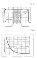
- Figure 1 shows a graph representing the continuous excitation and luminescent emission for a wafer such a silicon at a given position, where the horizontal axis is time and the vertical axis is emission intensity.
- the continuous intensity of the luminescence has an amplitude given by AcwP, where Acw is the amplitude of the excitation, and P is the probability that the excited energy gets reconverted to light.
- the hatched area represents the integrated intensity AcwPTm of the luminescence during a time Tm during which the measurement takes place.
- Figure 2 shows a graph representing the decaying light emission from a material such as silicon after light excitation, and the corresponding carrier lifetime position, with time as the horizontal axis and normalized emission intensity as the vertical axis.
- the probabilistic distribution is described by an exponential decay curve.
- the probability distribution for the light reemission is APe-t/ ⁇ (where e is the natural number) as shown in Figure 2 .
- This time T is to be defined as the carrier lifetime.
- the carrier lifetime ⁇ can be described as the time required for the 1/e fraction of the luminescence to decay with respect to its initial intensity.
- the graph of Figure 3 shows the relationship between time and the emission intensity from the material when given a sharp pulse of excitation.
- the thick continuous line of Figure 3 describes the light emission.
- the curve shows an increase of intensity during the sharp pulse, followed by a decrease in emission after the end of the excitation.
- the time integrated intensity of this emission described as the hatched region in Figure 3 , resulting from an excitation pulse of amplitude Ap during a time Tp, is simply PTpAp.
- This accumulated intensity of the emission has dependence on the emission probability P, however the carrier lifetime component still cannot be separated or extracted from it.
- the emission shown in Figure 3 shows the characteristic described in Figure 2 of the exponential decay APe-t/T on the falling edge in which carrier lifetime parameter T is convoluted.
- the decaying emission portion of Figure 3 following the increase and decrease of the excitation, is isolated in order to measure the carrier lifetime.
- the pulse duration can be very short, a very fast device for detecting the light is necessary.
- the decaying emission intensity can be very weak, it is necessary to have an apparatus that continuously and repeatedly acquires the emission signal in order to obtain a reasonable signal.
- the apparatus 1 of Figure 4 contains an excitation apparatus 10 and a detecting apparatus 20.
- the excitation apparatus 10 includes an excitation source 11 and a modulation device 12.
- the detecting apparatus 20 is composed of a modulation device 21, a filter 22 and a light accumulation device 23.
- the excitation source 11 is typically a continuous emission solid state laser while 12 and 21 are acousto-optic modulators.
- 23 is a device that integrates light by accumulating it over time and at specific positions, such as for example a CCD (charge coupled device) array.
- 22 is a wavelength filter or an optical polarization filter.
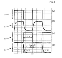
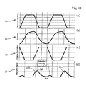
- the light 14 has a waveform described by excitation emitted by 11 and modulated by 12 and is shown in Figure 5 (a) .
- the continuous light 13 of Figure 4 enters the acousto-optic modulator 12 which rapidly switches its refractive index to allow light to pass.
- the intensity of the resulting light intensity at 14 therefore rises and drops in a square wave manner as described in Figure 5 (a) .
- the modulated light 14 shown in Figure 5 (a) has a duty ration of 50%.
- the luminescence 24 emitted from a semiconducting material 30 such as silicon excited by the modulated excitation 14 has intensity variations shown in Figure 5 (b) . Just like described in Figure 3 , the luminescence 24 sharply rises in intensity upon the start of the sharp excitation rise of 14, then shows decaying intensity when the excitation drops.
- the modulation waveform applied by the modulation device 21 on the detection side of the apparatus is shown in Figure 5 (c) .
- the modulator 21 is designed to be reversely synchronized with the modulated excitation 14 waveform shown in Figure 5 (a) , in such a way that when the excitation intensity drops in 14, the light begins to be allowed through in the acousto-optic modulation 21. Both modulators 12 and 21 and thus synchronized using a control signal and set to operate in such a mutually reversed modulation.
- the separated light 25, originating from the light 24 emitted from the semiconductor material 30 due to the modulated excitation 14, and allowed to pass by the modulator 21 is shown in Figure 5 (d) .
- the light allowed to pass through begins at the end of the excitation 14 therefore only contains the decaying intensity portion of the emission as shown in the hatched area 26.
- Figure 5 (b) represents the emission 24 of a single point from a certain area on the semiconductor material 30 from which the decaying light 26 is separated. The area of that single point is then reflected as a single pixel or cell of the CCD detector array in the detection apparatus 23.
- the intensity of light 25 shown in Figure 5 (d) then passes through filter 22 before reaching the detecting device 23, so that only some components of the decaying light 26 are extracted.
- the CCD detector cells of the detecting device 23 accumulate light during a certain integration time and the integrated intensity is then stored in memory. With respect to this integration time, the modulations of Figures 5 (a), (c) are much faster such that several cycles of the decaying light 25 shown in Figure 5 (d) can be accumulated in a single measurement.
- the carrier lifetime T characterizes the light 26, the decaying part of the emission immediately following the end of the excitation, and this light is accumulated multiple times by the measurement apparatus in order to effectively extract the carrier lifetime information.
- the decay light 26 accumulated by the detecting device 23 as an integrated intensity, and normalized with respect to their high frequency saturation value, is shown in the graph of Figure 6 , plotted as a function of the frequency of the excitation and detection modulation devices 12 and 21.
- the vertical axis shows the intensity, and the horizontal axis the modulation frequency.
- the resulting simulation of the intensity, for a fixed integration time, is shown in Figure 6 where the curves for discrete steps of material carrier lifetime of 50nsec, 70nsec, 100nsec, 150nsec, 200nsec, 300nsec and 500nsec are plotted.
- the graph of Figure 6 shows that at low modulation frequency, when the modulation period is much longer than the carrier lifetime parameter T, nearly no light or relatively very little of the emission decay light 26 is accumulated during the integration time. And as the frequency is increased, proportionally more and more of decayed light 26 is accumulated so that the intensity increases linearly.
- the theoretical saturation level of the intensity is 1 ⁇ 4 of the luminescence intensity AcwP shown in Figure 1 for the case of continuous excitation.
- Figure 6 shows a solid line at 50% of the saturation intensity for a series of different carrier life times. Near the crossing of the integrated intensity of each curve and the 50% line, a region of near-linear trend is seen as function of the logarithmic frequency scale is seen.
- a frequency in this range is desirable when selecting a single frequency for the excitation modulation frequency and the detection modulation frequency of the modulations shown in Figures 5 (a) and (c) respectively.
- Figure 6 shows that the normalized integrated intensity will increase for a longer carrier lifetime, or decrease for a shorter carrier lifetime.
- each of the measurement intensity should represent the carrier lifetime for that corresponding region of the material.
- the measured intensity should be high, and for short carrier lifetime the measured intensity should be low, such that the value of the carrier lifetime is directly represented by the intensity of the measured signal.
- the modulation frequency at which the integrated intensity is 50% of its saturation value is known as F
- the relationship described in Figure 7 is not limited to the carrier lifetime range 50nsec to 500nsec.
- the above relationship is not limited to the crossing when the integrated intensity reaches 50% of its saturation value.
- a similar linear relationship can be obtained for relative intensity crossings of, for example, 40% or 60%.
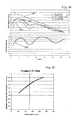
- Figures 9 through 11 show the simulated results of a method for extracting the carrier lifetime information, using assumed material properties of the emission probability and carrier lifetime as a function of position.
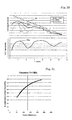
- Figure 9 shows the hypothetical simulation data for a material that has relatively different properties and trends for the emission probability and the carrier lifetime as function of position.
- the horizontal X axis represents position on the material. This material is assumed to have emission efficiency slowly decreasing from the left toward the right, while its carrier lifetime characteristics vary in a sort of wavelike trend as shown in the Figure.
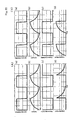
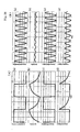
- Figure 10 (A) the simulated measurement at 1 MHz modulation is shown in Figure 10 (A) , where the applied excitation modulation 12 and the detection modulation 21 are reversed in phase.
- the waveforms of Figure 10 (A) are the same as those shown in Figure 5, (a) the excitation modulation waveform, (b) the waveform of the luminescence emitted from the material, (c) the detection side modulation, and (d) the resultant separated decaying portion of the light intensity.
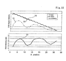
- Figure 11 shows a graph of this intensity as a function of position for a modulation frequency of 1 MHz as curve 31 plotted in a double dotted dashed line.
- Figure 10 (B) shows (a) the excitation modulation waveform, (b) the waveform of the luminescence emitted from the material, (c) the detection side modulation, and (d) the resultant separated decaying portion of the light intensity, where the applied excitation modulation 12 and the detection modulation 21 are reversed in phase, however for a modulation frequency of 10MHz.
- Figure 11 the resulting integrated intensity as a function of position is shown as curve 32 plotted in a continuous line.
- the excitation modulation of 12 and the detection modulation of 21 were assumed to have perfectly sharp square wave rise and drop characteristics, and moreover to be operating in perfect synchronization.
- an actual modulating device may not have the inability to produce such a square wave, slight deviations from perfect synchronizations and also the effects of noise in the system may affect the final modulation waveform characteristics.
- the present invention's method and apparatus can still extract the information related to the carrier lifetime as described above, even though deviations from perfect timing, from ideal excitation modulation waveform or from ideal detection modulation waveforms exist.
- the excitation light emitted by 11 is modulated by 12 resulting in a trapezoidal waveform shown in Figure 13 (a) .
- the light emitted by the material is shown in (b).
- a similar trapezoidal modulation is applied on the detector side by 21 and shown in (c).
- the modulation waveforms of (a) and (c) are modulating and synchronized at the same frequency and mutually reverse in phase.
- the waveform of the resulting light 25 which has been extracted from the luminescence 24 before reaching the detecting device 23, is shown in (d).
- a portion of the light 26a of light 25 shown in (d) does not contain only light from the decaying intensity, but also contains some portion of the light emitted during excitation.
- Figure 14 shows the result of applying the waveforms of Figure 13 (a) and (c) at a frequency of 1 MHz, where the double dotted dashed line 31 a represents the integrated intensity of the separated light 25 reaching the CCD detector.
- the resulting integrated intensity curve 32a is plotted as a continuous line in the Figure.
- the ratio of the intensity measured for 1 MHz modulation and the intensity measure for 10MH modulation is shown as trace 33a.
- This curve bears strong resemblance to the carrier lifetime data shown in Figure 9 . That is, even using the modulation characteristics of Figure 13 and using the ratio of the intensity obtained at 2 different frequencies, the information pertaining to the carrier lifetime can be extracted.
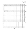
- an excitation resembling a sinusoidal waveform is used and shown in (a).
- the light emitted by the material 24 is shown in (b).
- a similar sinusoidal modulation is applied on the detector side and shown in (c).
- the modulation waveforms of (a) and (c) are modulating and synchronized at the same frequency and mutually reverse in phase.
- the waveform of the resulting light 25 which has been extracted from the luminescence 24 before reaching the detecting device 23, is shown in (d).
- a portion of the light 26a of light 25 shown in (d) does not contain only light from the decaying intensity, but also contains some portion of the light emitted during excitation.
- Figure 18 shows a near linear relationship between the carrier lifetime and the ratio of two integrated intensities measured at frequencies 1 MHz and 10MHz, as well as the ratio of these frequencies.
- Figure 18 hence shows that even for a sinusoidal modulation the measurement and ratio of 2 different modulation frequencies has a correspondence to the information relating to the carrier lifetime.
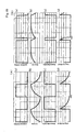
- the modulation waveforms of Figure 19 (A) are the same as those of 10 (A).
- a square wave excitation modulation is shown in (a) and a square wave detection modulation in (c).
- the waveforms in (a) and (c) are synchronized at 1 MHz and mutually opposite in phase.
- the separated light to be accumulated by the CCD during the integration is shown in (d).
- the result of applying this to the material properties as a function of position is shown in curve 31 c of Figure 20 plotted as a double dotted dashed line.
- the modulation waveforms of Figure 19 (B) are the same as those of Figure 16 , where the excitation modulation (a) and the detection modulation (c) are sinusoidal curves.
- the modulations of (a) and (c) are applied at the same frequency and are phase shifted by 180 degrees. Further, they are applied at the same 1 MHz frequency as the square wave modulations of Figure 19 (A) (a) and (c) .
- the result of this sinusoidal modulation is shown as curve 32c in Figure 20 , plotted as a solid line.
- the ratio of the square wave modulated intensity 31 c versus the sinusoidal wave modulated intensity 32c is shown as curve 33c of Figure 20 . It shows that this curve closely resembles the curve describing the carrier lifetime material data of Figure 9 .
- the ratio of the square wave modulated intensity versus the sinusoidal wave modulated intensity is plotted in Figure 21 with respect to nominal carrier lifetime. From Figure 21 , we see that the trend for increased intensity ratio corresponds to the increasing carrier lifetime.
- the simulation described by Figure 22 is the case where the ratio of the intensities is taken between two waveforms but for which the relative phase between the excitation modulation waveform and the detection modulation waveforms are offset.
- the modulation waveforms of Figure 22 (A) are the same as those of 10 (A) or 19 (A).
- the square waveforms in (a) and (c) are synchronized at 1 MHz and mutually phase shifted by 180 degrees.
- the separated light to be accumulated by the CCD during the integration is shown in (d).
- the result of applying this to the material properties as a function of position is shown in curve 31 d of Figure 23 plotted as a double dotted dashed line.
- the modulation waveforms of Figure 22 (B) display zero mutual phase shift. Both waveforms shown in (a) and (c) are square waves of duty ratio 50% applied synchronously at 1 MHz. The resulting distribution of applying this to the material properties is shown in figure 32d of Figure 23 .
- the ratio of the modulated intensity 31 d versus the modulated intensity 32d is shown as curve 33d of Figure 23 . It shows that this curve closely resembles the curve describing the carrier lifetime material data of Figure 9 .
- Figure 24 shows the relationship between nominal carrier lifetime and the ratio (integrated intensity resulting from modulations of Figure 22 (A) / integrated intensity resulting from modulations of Figure 22 (B) ). From Figure 24 we see that the carrier lifetime information can be extracted using the ratio of integrated intensities measured using different relatively phase-shifted square waves modulations on the detection side (c) with respect to the excitation square waves (a).
- the modulation waveforms of Figure 25 (A) are the same as those of Figures 10 (A ), 19 (A) or 21 (A) , where the excitation modulation is shown in (a) and the detection modulation is shown in (c) are mutually inverted square waves synchronized at 1 MHz.
- the modulation waveforms of Figure 25 (B) are also utually inverted square waves synchronized at 1 MHz with excitation modulation shown in (a) and detection modulation shown in (c).
- Figure 25 (A ) which shows modulations with duty ratio of 50:50
- those in Figure 25 (B) have a modulation duty ratio of 90:10.
- Figure 27 shows the relationship between nominal carrier lifetime and the ratio (integrated intensity resulting from modulations of Figure 25 (A) / integrated intensity resulting from modulations of Figure 25 (B)) . From Figure 27 we see that the carrier lifetime information can be extracted using the ratio of intensities measured using modulation waveforms of different duty ratios.
- the ratio of the intensity obtained using a square wave modulation at 1 MHz shown in Figure 28 (A) with respect to the intensity obtained using a sinusoidal wavelength modulated at 10 MHz shown in Figure 29 (B) can also be used to extract the information pertaining to the carrier lifetime.
- the apparatus 40 in the preferred embodiment of Figure 30 describes the ideal configuration for implementing the measurement method described up to this point.
- the excitation apparatus 10 is made up of an excitation source 11 and an excitation modulation device 12.
- the excitation source 11 is a solid state laser and the modulation device 12 an acousto-optic modulator.
- the light 13 emitted by the excitation source, modulated by 12 becomes the modulated excitation light 14.
- the lens 41 placed after the modulation device 12 serves to guide the excitation light 14 onto a certain region in an area of the material 30.
- Lens 41 can be a collimator lens, a large focusing lens, a defocusing lens or a combination of these, such that the excitation is optimized at the position of material 30.
- the detection apparatus 20 is made up of a modulation device 21 and a light detecting device 23.
- the modulation device 21 is an acousto-optic modulator.
- a collimator lens 42 is positioned between the material and the modulation device 21.
- the luminescence 24 emitted from the material 30 from a certain region passes through the collimator lens 42, some of that light passes through modulation device 21, such that the separated light 25 reaches the detecting device 23.
- the detecting device 23 is an array of detector cells from a CCD, before which a camera lens 43 is placed to focus the separated light 25.
- the detection device 21 can be equipped with filter 22 shown in Figure 4 if necessary.
- the luminescence 24 emitted from the material 30 from several positions in an area are integrated simultaneously by each of the CCD detector cell making it possible to obtain the carrier lifetime information and correlate that information with each position. Furthermore, for each of the CCD detector cell, the measured integrated intensity is processed and compared to obtain a distribution curve such as 33 in Figure 11 , in order to extract the information pertaining to the carrier lifetime of individual points within a large area on the material.
- material 30 can be moved step-wise or continuously in a direction normal to these rows by a translation motion device 45, in such a way that the CCD detector device 23 may sequentially acquire luminescence from a large area of material 30. This can also be accomplished by fixing the position of material 30 while moving the measurement apparatus 40.
- the measurement apparatus 40 is equipped with a modulation control unit 46. From this control unit 46, the excitation modulation device 12 and the detector modulation device 21 are controlled, and as shown in each Figure, applies modulations to the excitation light and the emitted light.
- the measurement apparatus 40 is also equipped with central control and processing unit 47, which controls the excitation source 11 as well as the modulation devices 12 and 21. Also, for each integration time during which the accumulated emission intensity is digitized by the CCD measurement device, saved to memory by the control and processing unit 47, where intensity ratios are taken resulting in curves such as shown in 33 of Figure 11 . For each detector cell of the CCD results a pixel with an intensity correlated to the carrier lifetime at a certain position within an area of material 30.
- the information processed by unit 47 giving the carrier life time for positions on the material within a certain area can then be displayed as carrier lifetime values in a table, or the result can be represented as a shade in an image. In the latter case each of the CCD detector cells are represented by a pixel in that image.
- the measurement apparatus 40A is equipped with a beam splitter 51 to separate the luminescence 24 emitted from material 30, then the separated light is collimated using a second camera lens 52. This portion of the emitted light does not go through the detector modulation device, and is accumulated by a second measurement device 53.
- the accumulation of both a modulated intensity of the luminescence 24 and non-modulated intensity of the luminescence 24 can be performed in a single measurement.
- a second modulation device could also be inserted between the beam splitter 51 and the detector device 53 in order to enable the measurement of two different modulations of the luminescence 24 in a single measurement.
- the present invention is not limited to the above embodiments.
- the excitation source 11 were an intermittently pulsed laser
- the modulation device 12 would not be required in order to obtain modulations with a variety of duty ratios.
- the detector device were such that it was possible to intermittently impede the signal from be accumulated into memory within that device, then even without the modulation device 21 it would be possible to isolate the decay luminescence, integrate that signal over a fixed integration time to similarly extract the carrier lifetime information.
- excitation source 10 it is also possible to replace the excitation source 10 with a device which is not a light source, but that can excite carriers within material 30 periodically using electrical excitation so that light is emitted during the electron-hole pair recombination via an electroluminescent process, thereby enabling measurement of the carrier lifetime.
Landscapes
- Health & Medical Sciences (AREA)
- Nuclear Medicine, Radiotherapy & Molecular Imaging (AREA)
- Physics & Mathematics (AREA)
- Life Sciences & Earth Sciences (AREA)
- Chemical & Material Sciences (AREA)
- Analytical Chemistry (AREA)
- Biochemistry (AREA)
- General Health & Medical Sciences (AREA)
- General Physics & Mathematics (AREA)
- Immunology (AREA)
- Pathology (AREA)
- Investigating, Analyzing Materials By Fluorescence Or Luminescence (AREA)
- Testing Or Measuring Of Semiconductors Or The Like (AREA)
Applications Claiming Priority (1)
| Application Number | Priority Date | Filing Date | Title |
|---|---|---|---|
| PCT/JP2011/053154 WO2012111093A1 (ja) | 2011-02-15 | 2011-02-15 | キャリア寿命の測定方法および測定装置 |
Publications (3)
| Publication Number | Publication Date |
|---|---|
| EP2677302A1 true EP2677302A1 (de) | 2013-12-25 |
| EP2677302A4 EP2677302A4 (de) | 2016-03-02 |
| EP2677302B1 EP2677302B1 (de) | 2017-10-11 |
Family
ID=46672058
Family Applications (1)
| Application Number | Title | Priority Date | Filing Date |
|---|---|---|---|
| EP11858857.3A Not-in-force EP2677302B1 (de) | 2011-02-15 | 2011-02-15 | Verfahren und vorrichtung zur messung der lebensdauer eines trägers |
Country Status (8)
| Country | Link |
|---|---|
| US (1) | US9029801B2 (de) |
| EP (1) | EP2677302B1 (de) |
| JP (1) | JP5843114B2 (de) |
| KR (1) | KR101506101B1 (de) |
| CN (1) | CN103080730B (de) |
| CA (1) | CA2805718C (de) |
| TW (1) | TWI567377B (de) |
| WO (1) | WO2012111093A1 (de) |
Cited By (1)
| Publication number | Priority date | Publication date | Assignee | Title |
|---|---|---|---|---|
| CN110208276A (zh) * | 2019-07-02 | 2019-09-06 | 长沙而道新能源科技有限公司 | 一种结构砼表观缺陷测定仪及其检测设备 |
Families Citing this family (14)
| Publication number | Priority date | Publication date | Assignee | Title |
|---|---|---|---|---|
| US9269034B2 (en) * | 2012-08-21 | 2016-02-23 | Empire Technology Development Llc | Orthogonal encoding for tags |
| DE102013109010B4 (de) | 2013-08-21 | 2019-03-14 | Presens - Precision Sensing Gmbh | Verfahren zur Bestimmung einer Veränderlichen einer Probe |
| DE102013112885A1 (de) * | 2013-11-21 | 2015-05-21 | Osram Opto Semiconductors Gmbh | Verfahren zur optischen Charakterisierung eines optoelektronischen Halbleitermaterials und Vorrichtung zur Durchführung des Verfahrens |
| DE102015111213B4 (de) * | 2015-07-10 | 2023-05-04 | Infineon Technologies Ag | Verfahren zum Verringern einer bipolaren Degradation bei einem SiC-Halbleiterbauelement und Halbleiterbauelement |
| WO2017082218A1 (ja) * | 2015-11-09 | 2017-05-18 | 国立研究開発法人理化学研究所 | 光子検出装置、光子検出方法、蛍光相関分光測定装置、蛍光相互相関分光測定装置、動的光散乱測定装置、及び、蛍光顕微鏡 |
| CN105629147A (zh) * | 2015-12-28 | 2016-06-01 | 清华大学 | Led载流子寿命测试系统 |
| FR3066590A1 (fr) * | 2017-05-22 | 2018-11-23 | Centre National De La Recherche Scientifique - Cnrs - | Spectroscopie quantitative de densite de defauts electroniques dans un photorecepteur en couches minces, notamment dans une cellule solaire |
| JP7000198B2 (ja) | 2018-02-16 | 2022-01-19 | 浜松ホトニクス株式会社 | キャリア寿命測定方法及びキャリア寿命測定装置 |
| US10935492B2 (en) * | 2018-04-13 | 2021-03-02 | Applied Materials, Inc. | Metrology for OLED manufacturing using photoluminescence spectroscopy |
| CN110470965B (zh) * | 2019-07-09 | 2020-07-28 | 同济大学 | 一种半导体表面态载流子寿命测试方法 |
| WO2023126910A2 (en) | 2022-01-03 | 2023-07-06 | Einat Ronen | Multi-modal diagnostic device and database service for ophthalmology and neurology |
| KR102704988B1 (ko) * | 2022-02-07 | 2024-09-06 | 한국에너지기술연구원 | 캐리어 수명 측정 장치 및 방법 |
| EP4257958A1 (de) * | 2022-04-05 | 2023-10-11 | Centre national de la recherche scientifique | Verfahren und vorrichtung zur bestimmung der effektiven elektronenlebensdauer in einer probe |
| WO2025084986A1 (en) * | 2023-10-17 | 2025-04-24 | National University Of Singapore | Method and system for luminescence characterisation of a semiconductor device |
Family Cites Families (18)
| Publication number | Priority date | Publication date | Assignee | Title |
|---|---|---|---|---|
| JPS6017327A (ja) * | 1983-07-08 | 1985-01-29 | Omron Tateisi Electronics Co | 温度測定装置 |
| JPS63312649A (ja) | 1987-06-16 | 1988-12-21 | Kawasaki Steel Corp | 半導体中の不純物準位およびキャリヤ寿命同時測定方法 |
| JP2889307B2 (ja) * | 1990-03-26 | 1999-05-10 | 株式会社東芝 | ▲iv▼族半導体のキャリアライフタイム測定法 |
| JPH0410574A (ja) | 1990-04-27 | 1992-01-14 | Nec Corp | 半導体装置 |
| JPH0714893A (ja) | 1993-06-21 | 1995-01-17 | Sumitomo Metal Mining Co Ltd | 半導体中の多数キャリア寿命の測定方法 |
| JPH10267844A (ja) * | 1997-03-25 | 1998-10-09 | Jasco Corp | 時間分解蛍光検出器およびそれを用いた蛍光分析装置、方法 |
| DE10056770A1 (de) * | 2000-11-14 | 2002-05-23 | Barre Stephan | Verfahren und Vorrichtung zur Messung von Eigenschaften einer Probe in mehreren Punkten der Probe |
| TW508714B (en) * | 2001-12-21 | 2002-11-01 | Chen Miin Jang | Inspection method of interface quality between silicon semiconductor and gate insulation layer in metal oxide semiconductor device |
| JP2003207453A (ja) * | 2002-01-16 | 2003-07-25 | Hitachi High-Technologies Corp | 蛍光,燐光測定装置 |
| JP4188653B2 (ja) * | 2002-10-01 | 2008-11-26 | 浜松ホトニクス株式会社 | 蛍光測定装置 |
| US6965431B2 (en) | 2003-02-28 | 2005-11-15 | Ut-Battelle, Llc | Integrated tunable optical sensor (ITOS) system |
| JP2005091346A (ja) * | 2003-08-14 | 2005-04-07 | Taiyo Denki Kk | 蛍光検出方法および蛍光検出装置 |
| JP2006038638A (ja) * | 2004-07-27 | 2006-02-09 | Matsushita Electric Ind Co Ltd | 半導体膜の品質を検査するための検査システム及びこれを用いた検査方法 |
| CN103185854B (zh) | 2006-05-05 | 2015-07-01 | Bt成像股份有限公司 | 利用发光成像测试间接带隙半导体器件的方法和系统 |
| JP5093795B2 (ja) | 2007-01-11 | 2012-12-12 | 株式会社フジクラ | 蛍光寿命測定装置及び成膜装置、蛍光寿命測定方法 |
| EP2108129A4 (de) | 2007-01-30 | 2013-06-12 | Ge Healthcare Bio Sciences | Zeitgesteuertes fluoreszenz-abbildungssystem |
| DE102008013068B4 (de) * | 2008-03-06 | 2012-06-21 | Institut Für Solarenergieforschung Gmbh | Verfahren und Vorrichtung zur ortsaufgelösten Bestimmung von Ladungsträgerlebensdauern in Halbleiterstrukturen |
| DE102008044879A1 (de) * | 2008-08-29 | 2010-03-04 | Fraunhofer-Gesellschaft zur Förderung der angewandten Forschung e.V. | Verfahren zur Bestimmung der Überschussladungsträgerlebensdauer in einer Halbleiterschicht |
-
2011
- 2011-02-15 US US13/817,062 patent/US9029801B2/en active Active
- 2011-02-15 JP JP2012557699A patent/JP5843114B2/ja not_active Expired - Fee Related
- 2011-02-15 CN CN201180041790.2A patent/CN103080730B/zh not_active Expired - Fee Related
- 2011-02-15 CA CA2805718A patent/CA2805718C/en active Active
- 2011-02-15 KR KR1020137004053A patent/KR101506101B1/ko not_active Expired - Fee Related
- 2011-02-15 EP EP11858857.3A patent/EP2677302B1/de not_active Not-in-force
- 2011-02-15 WO PCT/JP2011/053154 patent/WO2012111093A1/ja not_active Ceased
-
2012
- 2012-02-14 TW TW101104715A patent/TWI567377B/zh not_active IP Right Cessation
Non-Patent Citations (1)
| Title |
|---|
| See references of WO2012111093A1 * |
Cited By (2)
| Publication number | Priority date | Publication date | Assignee | Title |
|---|---|---|---|---|
| CN110208276A (zh) * | 2019-07-02 | 2019-09-06 | 长沙而道新能源科技有限公司 | 一种结构砼表观缺陷测定仪及其检测设备 |
| CN110208276B (zh) * | 2019-07-02 | 2023-03-31 | 广州越监工程质量安全检测中心有限公司 | 一种结构砼表观缺陷测定仪及其检测设备 |
Also Published As
| Publication number | Publication date |
|---|---|
| JP5843114B2 (ja) | 2016-01-13 |
| WO2012111093A1 (ja) | 2012-08-23 |
| CN103080730B (zh) | 2016-03-09 |
| CA2805718C (en) | 2016-04-12 |
| US20130140431A1 (en) | 2013-06-06 |
| US9029801B2 (en) | 2015-05-12 |
| TW201250230A (en) | 2012-12-16 |
| JPWO2012111093A1 (ja) | 2014-07-03 |
| TWI567377B (zh) | 2017-01-21 |
| KR20130054355A (ko) | 2013-05-24 |
| EP2677302A4 (de) | 2016-03-02 |
| KR101506101B1 (ko) | 2015-03-25 |
| CA2805718A1 (en) | 2012-08-23 |
| EP2677302B1 (de) | 2017-10-11 |
| CN103080730A (zh) | 2013-05-01 |
Similar Documents
| Publication | Publication Date | Title |
|---|---|---|
| EP2677302B1 (de) | Verfahren und vorrichtung zur messung der lebensdauer eines trägers | |
| KR101096629B1 (ko) | 전계 발광 시료 분석 장치 | |
| TWI641851B (zh) | 用於在發光二極體結構中之內部量子效率之非接觸量測的方法及裝置 | |
| JP2975815B2 (ja) | 半導体発光素子の評価装置及び評価方法 | |
| JP6565112B2 (ja) | 太陽電池の評価方法及び評価装置 | |
| CN101339092A (zh) | Led芯片/晶圆/外延片的非接触式检测方法及检测装置 | |
| CN101561475A (zh) | 一种led发光特性的非接触检测方法及装置 | |
| KR102812847B1 (ko) | 펄스 전류에 의해 여기되는 순간 흡수 분광기 | |
| Kasemann et al. | Spatially resolved silicon solar cell characterization using infrared imaging methods | |
| JPH0864652A (ja) | エピタキシャルウェハの検査方法 | |
| CN114779036B (zh) | 具有时间和空间分辨力的功率器件热分布测量方法及系统 | |
| CN106199368B (zh) | 非接触硅基光电器件少数载流子寿命检测仪及检测方法 | |
| JP3011504B2 (ja) | 半導体発光素子の評価装置 | |
| US7480043B2 (en) | Method for analyzing the reliability of optoelectronic elements rapidly | |
| JPH05251537A (ja) | ウエハフォトルミネスセンスマッピング装置 | |
| Lin et al. | Ultrafast Gated Hyperspectral Imaging System for Spatial-Spectral-Temporal-Resolved Electroluminescence of Miniaturized Light-Emitting Diodes | |
| KR20080088971A (ko) | 실리콘 웨이퍼의 결정 구조 분석 방법 | |
| Jacob et al. | Recombination Analysis of Maxeon IBC Production Cells by Time-Resolved Photoluminescence | |
| WO2025084986A1 (en) | Method and system for luminescence characterisation of a semiconductor device | |
| CN113984727A (zh) | 一种半导体缺陷对荧光寿命影响的检测装置及检测方法 | |
| Azkona et al. | Characterization of silicon solar cells by means of their luminescence under high frequency sinusoidal excitations | |
| JPH04139852A (ja) | 半導体基板の検査方法 |
Legal Events
| Date | Code | Title | Description |
|---|---|---|---|
| PUAI | Public reference made under article 153(3) epc to a published international application that has entered the european phase |
Free format text: ORIGINAL CODE: 0009012 |
|
| 17P | Request for examination filed |
Effective date: 20130130 |
|
| AK | Designated contracting states |
Kind code of ref document: A1 Designated state(s): AL AT BE BG CH CY CZ DE DK EE ES FI FR GB GR HR HU IE IS IT LI LT LU LV MC MK MT NL NO PL PT RO RS SE SI SK SM TR |
|
| DAX | Request for extension of the european patent (deleted) | ||
| RA4 | Supplementary search report drawn up and despatched (corrected) |
Effective date: 20160203 |
|
| RIC1 | Information provided on ipc code assigned before grant |
Ipc: G01R 31/265 20060101ALI20160128BHEP Ipc: H01L 21/66 20060101ALI20160128BHEP Ipc: G01N 21/64 20060101AFI20160128BHEP |
|
| GRAP | Despatch of communication of intention to grant a patent |
Free format text: ORIGINAL CODE: EPIDOSNIGR1 |
|
| RIC1 | Information provided on ipc code assigned before grant |
Ipc: G01R 31/265 20060101ALI20170308BHEP Ipc: G01N 21/17 20060101ALI20170308BHEP Ipc: H01L 21/66 20060101ALI20170308BHEP Ipc: G01N 21/64 20060101AFI20170308BHEP |
|
| INTG | Intention to grant announced |
Effective date: 20170328 |
|
| GRAS | Grant fee paid |
Free format text: ORIGINAL CODE: EPIDOSNIGR3 |
|
| GRAA | (expected) grant |
Free format text: ORIGINAL CODE: 0009210 |
|
| AK | Designated contracting states |
Kind code of ref document: B1 Designated state(s): AL AT BE BG CH CY CZ DE DK EE ES FI FR GB GR HR HU IE IS IT LI LT LU LV MC MK MT NL NO PL PT RO RS SE SI SK SM TR |
|
| REG | Reference to a national code |
Ref country code: GB Ref legal event code: FG4D |
|
| REG | Reference to a national code |
Ref country code: CH Ref legal event code: EP |
|
| REG | Reference to a national code |
Ref country code: IE Ref legal event code: FG4D |
|
| REG | Reference to a national code |
Ref country code: AT Ref legal event code: REF Ref document number: 936486 Country of ref document: AT Kind code of ref document: T Effective date: 20171115 |
|
| REG | Reference to a national code |
Ref country code: DE Ref legal event code: R096 Ref document number: 602011042407 Country of ref document: DE |
|
| REG | Reference to a national code |
Ref country code: NL Ref legal event code: MP Effective date: 20171011 |
|
| REG | Reference to a national code |
Ref country code: LT Ref legal event code: MG4D |
|
| REG | Reference to a national code |
Ref country code: AT Ref legal event code: MK05 Ref document number: 936486 Country of ref document: AT Kind code of ref document: T Effective date: 20171011 |
|
| PG25 | Lapsed in a contracting state [announced via postgrant information from national office to epo] |
Ref country code: NL Free format text: LAPSE BECAUSE OF FAILURE TO SUBMIT A TRANSLATION OF THE DESCRIPTION OR TO PAY THE FEE WITHIN THE PRESCRIBED TIME-LIMIT Effective date: 20171011 |
|
| PG25 | Lapsed in a contracting state [announced via postgrant information from national office to epo] |
Ref country code: LT Free format text: LAPSE BECAUSE OF FAILURE TO SUBMIT A TRANSLATION OF THE DESCRIPTION OR TO PAY THE FEE WITHIN THE PRESCRIBED TIME-LIMIT Effective date: 20171011 Ref country code: SE Free format text: LAPSE BECAUSE OF FAILURE TO SUBMIT A TRANSLATION OF THE DESCRIPTION OR TO PAY THE FEE WITHIN THE PRESCRIBED TIME-LIMIT Effective date: 20171011 Ref country code: FI Free format text: LAPSE BECAUSE OF FAILURE TO SUBMIT A TRANSLATION OF THE DESCRIPTION OR TO PAY THE FEE WITHIN THE PRESCRIBED TIME-LIMIT Effective date: 20171011 Ref country code: ES Free format text: LAPSE BECAUSE OF FAILURE TO SUBMIT A TRANSLATION OF THE DESCRIPTION OR TO PAY THE FEE WITHIN THE PRESCRIBED TIME-LIMIT Effective date: 20171011 Ref country code: NO Free format text: LAPSE BECAUSE OF FAILURE TO SUBMIT A TRANSLATION OF THE DESCRIPTION OR TO PAY THE FEE WITHIN THE PRESCRIBED TIME-LIMIT Effective date: 20180111 |
|
| PG25 | Lapsed in a contracting state [announced via postgrant information from national office to epo] |
Ref country code: IS Free format text: LAPSE BECAUSE OF FAILURE TO SUBMIT A TRANSLATION OF THE DESCRIPTION OR TO PAY THE FEE WITHIN THE PRESCRIBED TIME-LIMIT Effective date: 20180211 Ref country code: BG Free format text: LAPSE BECAUSE OF FAILURE TO SUBMIT A TRANSLATION OF THE DESCRIPTION OR TO PAY THE FEE WITHIN THE PRESCRIBED TIME-LIMIT Effective date: 20180111 Ref country code: HR Free format text: LAPSE BECAUSE OF FAILURE TO SUBMIT A TRANSLATION OF THE DESCRIPTION OR TO PAY THE FEE WITHIN THE PRESCRIBED TIME-LIMIT Effective date: 20171011 Ref country code: AT Free format text: LAPSE BECAUSE OF FAILURE TO SUBMIT A TRANSLATION OF THE DESCRIPTION OR TO PAY THE FEE WITHIN THE PRESCRIBED TIME-LIMIT Effective date: 20171011 Ref country code: LV Free format text: LAPSE BECAUSE OF FAILURE TO SUBMIT A TRANSLATION OF THE DESCRIPTION OR TO PAY THE FEE WITHIN THE PRESCRIBED TIME-LIMIT Effective date: 20171011 Ref country code: GR Free format text: LAPSE BECAUSE OF FAILURE TO SUBMIT A TRANSLATION OF THE DESCRIPTION OR TO PAY THE FEE WITHIN THE PRESCRIBED TIME-LIMIT Effective date: 20180112 Ref country code: RS Free format text: LAPSE BECAUSE OF FAILURE TO SUBMIT A TRANSLATION OF THE DESCRIPTION OR TO PAY THE FEE WITHIN THE PRESCRIBED TIME-LIMIT Effective date: 20171011 |
|
| REG | Reference to a national code |
Ref country code: DE Ref legal event code: R097 Ref document number: 602011042407 Country of ref document: DE |
|
| PG25 | Lapsed in a contracting state [announced via postgrant information from national office to epo] |
Ref country code: DK Free format text: LAPSE BECAUSE OF FAILURE TO SUBMIT A TRANSLATION OF THE DESCRIPTION OR TO PAY THE FEE WITHIN THE PRESCRIBED TIME-LIMIT Effective date: 20171011 Ref country code: CZ Free format text: LAPSE BECAUSE OF FAILURE TO SUBMIT A TRANSLATION OF THE DESCRIPTION OR TO PAY THE FEE WITHIN THE PRESCRIBED TIME-LIMIT Effective date: 20171011 Ref country code: EE Free format text: LAPSE BECAUSE OF FAILURE TO SUBMIT A TRANSLATION OF THE DESCRIPTION OR TO PAY THE FEE WITHIN THE PRESCRIBED TIME-LIMIT Effective date: 20171011 Ref country code: SK Free format text: LAPSE BECAUSE OF FAILURE TO SUBMIT A TRANSLATION OF THE DESCRIPTION OR TO PAY THE FEE WITHIN THE PRESCRIBED TIME-LIMIT Effective date: 20171011 |
|
| PLBE | No opposition filed within time limit |
Free format text: ORIGINAL CODE: 0009261 |
|
| STAA | Information on the status of an ep patent application or granted ep patent |
Free format text: STATUS: NO OPPOSITION FILED WITHIN TIME LIMIT |
|
| PG25 | Lapsed in a contracting state [announced via postgrant information from national office to epo] |
Ref country code: RO Free format text: LAPSE BECAUSE OF FAILURE TO SUBMIT A TRANSLATION OF THE DESCRIPTION OR TO PAY THE FEE WITHIN THE PRESCRIBED TIME-LIMIT Effective date: 20171011 Ref country code: IT Free format text: LAPSE BECAUSE OF FAILURE TO SUBMIT A TRANSLATION OF THE DESCRIPTION OR TO PAY THE FEE WITHIN THE PRESCRIBED TIME-LIMIT Effective date: 20171011 Ref country code: SM Free format text: LAPSE BECAUSE OF FAILURE TO SUBMIT A TRANSLATION OF THE DESCRIPTION OR TO PAY THE FEE WITHIN THE PRESCRIBED TIME-LIMIT Effective date: 20171011 Ref country code: PL Free format text: LAPSE BECAUSE OF FAILURE TO SUBMIT A TRANSLATION OF THE DESCRIPTION OR TO PAY THE FEE WITHIN THE PRESCRIBED TIME-LIMIT Effective date: 20171011 |
|
| REG | Reference to a national code |
Ref country code: CH Ref legal event code: PL |
|
| 26N | No opposition filed |
Effective date: 20180712 |
|
| PG25 | Lapsed in a contracting state [announced via postgrant information from national office to epo] |
Ref country code: MC Free format text: LAPSE BECAUSE OF FAILURE TO SUBMIT A TRANSLATION OF THE DESCRIPTION OR TO PAY THE FEE WITHIN THE PRESCRIBED TIME-LIMIT Effective date: 20171011 |
|
| REG | Reference to a national code |
Ref country code: IE Ref legal event code: MM4A |
|
| REG | Reference to a national code |
Ref country code: BE Ref legal event code: MM Effective date: 20180228 |
|
| PG25 | Lapsed in a contracting state [announced via postgrant information from national office to epo] |
Ref country code: LU Free format text: LAPSE BECAUSE OF NON-PAYMENT OF DUE FEES Effective date: 20180215 Ref country code: SI Free format text: LAPSE BECAUSE OF FAILURE TO SUBMIT A TRANSLATION OF THE DESCRIPTION OR TO PAY THE FEE WITHIN THE PRESCRIBED TIME-LIMIT Effective date: 20171011 Ref country code: CH Free format text: LAPSE BECAUSE OF NON-PAYMENT OF DUE FEES Effective date: 20180228 Ref country code: LI Free format text: LAPSE BECAUSE OF NON-PAYMENT OF DUE FEES Effective date: 20180228 |
|
| REG | Reference to a national code |
Ref country code: FR Ref legal event code: ST Effective date: 20181031 |
|
| PG25 | Lapsed in a contracting state [announced via postgrant information from national office to epo] |
Ref country code: IE Free format text: LAPSE BECAUSE OF NON-PAYMENT OF DUE FEES Effective date: 20180215 |
|
| PG25 | Lapsed in a contracting state [announced via postgrant information from national office to epo] |
Ref country code: BE Free format text: LAPSE BECAUSE OF NON-PAYMENT OF DUE FEES Effective date: 20180228 Ref country code: FR Free format text: LAPSE BECAUSE OF NON-PAYMENT OF DUE FEES Effective date: 20180228 |
|
| PG25 | Lapsed in a contracting state [announced via postgrant information from national office to epo] |
Ref country code: MT Free format text: LAPSE BECAUSE OF NON-PAYMENT OF DUE FEES Effective date: 20180215 |
|
| PG25 | Lapsed in a contracting state [announced via postgrant information from national office to epo] |
Ref country code: TR Free format text: LAPSE BECAUSE OF FAILURE TO SUBMIT A TRANSLATION OF THE DESCRIPTION OR TO PAY THE FEE WITHIN THE PRESCRIBED TIME-LIMIT Effective date: 20171011 |
|
| PG25 | Lapsed in a contracting state [announced via postgrant information from national office to epo] |
Ref country code: PT Free format text: LAPSE BECAUSE OF FAILURE TO SUBMIT A TRANSLATION OF THE DESCRIPTION OR TO PAY THE FEE WITHIN THE PRESCRIBED TIME-LIMIT Effective date: 20171011 Ref country code: HU Free format text: LAPSE BECAUSE OF FAILURE TO SUBMIT A TRANSLATION OF THE DESCRIPTION OR TO PAY THE FEE WITHIN THE PRESCRIBED TIME-LIMIT; INVALID AB INITIO Effective date: 20110215 |
|
| PG25 | Lapsed in a contracting state [announced via postgrant information from national office to epo] |
Ref country code: CY Free format text: LAPSE BECAUSE OF FAILURE TO SUBMIT A TRANSLATION OF THE DESCRIPTION OR TO PAY THE FEE WITHIN THE PRESCRIBED TIME-LIMIT Effective date: 20171011 Ref country code: MK Free format text: LAPSE BECAUSE OF NON-PAYMENT OF DUE FEES Effective date: 20171011 |
|
| PG25 | Lapsed in a contracting state [announced via postgrant information from national office to epo] |
Ref country code: AL Free format text: LAPSE BECAUSE OF FAILURE TO SUBMIT A TRANSLATION OF THE DESCRIPTION OR TO PAY THE FEE WITHIN THE PRESCRIBED TIME-LIMIT Effective date: 20171011 |
|
| PGFP | Annual fee paid to national office [announced via postgrant information from national office to epo] |
Ref country code: GB Payment date: 20220209 Year of fee payment: 12 |
|
| PGFP | Annual fee paid to national office [announced via postgrant information from national office to epo] |
Ref country code: DE Payment date: 20220421 Year of fee payment: 12 |
|
| REG | Reference to a national code |
Ref country code: DE Ref legal event code: R119 Ref document number: 602011042407 Country of ref document: DE |
|
| GBPC | Gb: european patent ceased through non-payment of renewal fee |
Effective date: 20230215 |
|
| PG25 | Lapsed in a contracting state [announced via postgrant information from national office to epo] |
Ref country code: GB Free format text: LAPSE BECAUSE OF NON-PAYMENT OF DUE FEES Effective date: 20230215 |
|
| PG25 | Lapsed in a contracting state [announced via postgrant information from national office to epo] |
Ref country code: GB Free format text: LAPSE BECAUSE OF NON-PAYMENT OF DUE FEES Effective date: 20230215 Ref country code: DE Free format text: LAPSE BECAUSE OF NON-PAYMENT OF DUE FEES Effective date: 20230901 |