EP2690666A1 - Procédé de fabrication d'un élément de conversion photoélectrique - Google Patents
Procédé de fabrication d'un élément de conversion photoélectrique Download PDFInfo
- Publication number
- EP2690666A1 EP2690666A1 EP12763547.2A EP12763547A EP2690666A1 EP 2690666 A1 EP2690666 A1 EP 2690666A1 EP 12763547 A EP12763547 A EP 12763547A EP 2690666 A1 EP2690666 A1 EP 2690666A1
- Authority
- EP
- European Patent Office
- Prior art keywords
- layer
- amorphous silicon
- type amorphous
- type
- silicon layer
- Prior art date
- Legal status (The legal status is an assumption and is not a legal conclusion. Google has not performed a legal analysis and makes no representation as to the accuracy of the status listed.)
- Ceased
Links
Images




Classifications
-
- H—ELECTRICITY
- H10—SEMICONDUCTOR DEVICES; ELECTRIC SOLID-STATE DEVICES NOT OTHERWISE PROVIDED FOR
- H10F—INORGANIC SEMICONDUCTOR DEVICES SENSITIVE TO INFRARED RADIATION, LIGHT, ELECTROMAGNETIC RADIATION OF SHORTER WAVELENGTH OR CORPUSCULAR RADIATION
- H10F71/00—Manufacture or treatment of devices covered by this subclass
- H10F71/10—Manufacture or treatment of devices covered by this subclass the devices comprising amorphous semiconductor material
-
- H—ELECTRICITY
- H10—SEMICONDUCTOR DEVICES; ELECTRIC SOLID-STATE DEVICES NOT OTHERWISE PROVIDED FOR
- H10F—INORGANIC SEMICONDUCTOR DEVICES SENSITIVE TO INFRARED RADIATION, LIGHT, ELECTROMAGNETIC RADIATION OF SHORTER WAVELENGTH OR CORPUSCULAR RADIATION
- H10F10/00—Individual photovoltaic cells, e.g. solar cells
- H10F10/10—Individual photovoltaic cells, e.g. solar cells having potential barriers
- H10F10/14—Photovoltaic cells having only PN homojunction potential barriers
- H10F10/146—Back-junction photovoltaic cells, e.g. having interdigitated base-emitter regions on the back side
-
- H—ELECTRICITY
- H10—SEMICONDUCTOR DEVICES; ELECTRIC SOLID-STATE DEVICES NOT OTHERWISE PROVIDED FOR
- H10F—INORGANIC SEMICONDUCTOR DEVICES SENSITIVE TO INFRARED RADIATION, LIGHT, ELECTROMAGNETIC RADIATION OF SHORTER WAVELENGTH OR CORPUSCULAR RADIATION
- H10F10/00—Individual photovoltaic cells, e.g. solar cells
- H10F10/10—Individual photovoltaic cells, e.g. solar cells having potential barriers
- H10F10/16—Photovoltaic cells having only PN heterojunction potential barriers
- H10F10/164—Photovoltaic cells having only PN heterojunction potential barriers comprising heterojunctions with Group IV materials, e.g. ITO/Si or GaAs/SiGe photovoltaic cells
- H10F10/165—Photovoltaic cells having only PN heterojunction potential barriers comprising heterojunctions with Group IV materials, e.g. ITO/Si or GaAs/SiGe photovoltaic cells the heterojunctions being Group IV-IV heterojunctions, e.g. Si/Ge, SiGe/Si or Si/SiC photovoltaic cells
- H10F10/166—Photovoltaic cells having only PN heterojunction potential barriers comprising heterojunctions with Group IV materials, e.g. ITO/Si or GaAs/SiGe photovoltaic cells the heterojunctions being Group IV-IV heterojunctions, e.g. Si/Ge, SiGe/Si or Si/SiC photovoltaic cells the Group IV-IV heterojunctions being heterojunctions of crystalline and amorphous materials, e.g. silicon heterojunction [SHJ] photovoltaic cells
-
- H—ELECTRICITY
- H10—SEMICONDUCTOR DEVICES; ELECTRIC SOLID-STATE DEVICES NOT OTHERWISE PROVIDED FOR
- H10F—INORGANIC SEMICONDUCTOR DEVICES SENSITIVE TO INFRARED RADIATION, LIGHT, ELECTROMAGNETIC RADIATION OF SHORTER WAVELENGTH OR CORPUSCULAR RADIATION
- H10F71/00—Manufacture or treatment of devices covered by this subclass
- H10F71/10—Manufacture or treatment of devices covered by this subclass the devices comprising amorphous semiconductor material
- H10F71/103—Manufacture or treatment of devices covered by this subclass the devices comprising amorphous semiconductor material including only Group IV materials
-
- H—ELECTRICITY
- H10—SEMICONDUCTOR DEVICES; ELECTRIC SOLID-STATE DEVICES NOT OTHERWISE PROVIDED FOR
- H10F—INORGANIC SEMICONDUCTOR DEVICES SENSITIVE TO INFRARED RADIATION, LIGHT, ELECTROMAGNETIC RADIATION OF SHORTER WAVELENGTH OR CORPUSCULAR RADIATION
- H10F77/00—Constructional details of devices covered by this subclass
- H10F77/10—Semiconductor bodies
- H10F77/14—Shape of semiconductor bodies; Shapes, relative sizes or dispositions of semiconductor regions within semiconductor bodies
- H10F77/148—Shapes of potential barriers
-
- H—ELECTRICITY
- H10—SEMICONDUCTOR DEVICES; ELECTRIC SOLID-STATE DEVICES NOT OTHERWISE PROVIDED FOR
- H10F—INORGANIC SEMICONDUCTOR DEVICES SENSITIVE TO INFRARED RADIATION, LIGHT, ELECTROMAGNETIC RADIATION OF SHORTER WAVELENGTH OR CORPUSCULAR RADIATION
- H10F77/00—Constructional details of devices covered by this subclass
- H10F77/20—Electrodes
- H10F77/206—Electrodes for devices having potential barriers
- H10F77/211—Electrodes for devices having potential barriers for photovoltaic cells
- H10F77/219—Arrangements for electrodes of back-contact photovoltaic cells
-
- H—ELECTRICITY
- H10—SEMICONDUCTOR DEVICES; ELECTRIC SOLID-STATE DEVICES NOT OTHERWISE PROVIDED FOR
- H10F—INORGANIC SEMICONDUCTOR DEVICES SENSITIVE TO INFRARED RADIATION, LIGHT, ELECTROMAGNETIC RADIATION OF SHORTER WAVELENGTH OR CORPUSCULAR RADIATION
- H10F77/00—Constructional details of devices covered by this subclass
- H10F77/30—Coatings
- H10F77/306—Coatings for devices having potential barriers
- H10F77/311—Coatings for devices having potential barriers for photovoltaic cells
-
- Y—GENERAL TAGGING OF NEW TECHNOLOGICAL DEVELOPMENTS; GENERAL TAGGING OF CROSS-SECTIONAL TECHNOLOGIES SPANNING OVER SEVERAL SECTIONS OF THE IPC; TECHNICAL SUBJECTS COVERED BY FORMER USPC CROSS-REFERENCE ART COLLECTIONS [XRACs] AND DIGESTS
- Y02—TECHNOLOGIES OR APPLICATIONS FOR MITIGATION OR ADAPTATION AGAINST CLIMATE CHANGE
- Y02E—REDUCTION OF GREENHOUSE GAS [GHG] EMISSIONS, RELATED TO ENERGY GENERATION, TRANSMISSION OR DISTRIBUTION
- Y02E10/00—Energy generation through renewable energy sources
- Y02E10/50—Photovoltaic [PV] energy
- Y02E10/547—Monocrystalline silicon PV cells
-
- Y—GENERAL TAGGING OF NEW TECHNOLOGICAL DEVELOPMENTS; GENERAL TAGGING OF CROSS-SECTIONAL TECHNOLOGIES SPANNING OVER SEVERAL SECTIONS OF THE IPC; TECHNICAL SUBJECTS COVERED BY FORMER USPC CROSS-REFERENCE ART COLLECTIONS [XRACs] AND DIGESTS
- Y02—TECHNOLOGIES OR APPLICATIONS FOR MITIGATION OR ADAPTATION AGAINST CLIMATE CHANGE
- Y02P—CLIMATE CHANGE MITIGATION TECHNOLOGIES IN THE PRODUCTION OR PROCESSING OF GOODS
- Y02P70/00—Climate change mitigation technologies in the production process for final industrial or consumer products
- Y02P70/50—Manufacturing or production processes characterised by the final manufactured product
Definitions
- the present invention relates to a method of producing a photovoltaic element.
- Patent Document 1 discloses a photovoltaic element comprising a semiconductor substrate comprising monocrystalline silicon and having a light-receiving surface and a back surface provided on a side opposite the light-receiving surface; a first semiconductor layer and a second semiconductor layer comprising amorphous silicon, formed along a predetermined direction over the back surface, and in which layers of different conductive types are alternately placed along the back surface; an insulating layer formed straddling from a region over the second semiconductor layer to a region over the first semiconductor layer; a transparent electrode layer covering the first semiconductor layer and the second semiconductor layer; and a collective electrode layer formed over the transparent electrode layer.
- characteristics of an interface between a semiconductor substrate comprising monocrystalline silicon and a semiconductor layer comprising amorphous silicon significantly affect the power generation efficiency.
- a contact resistance or the like in the electricity-collecting electrode in which carriers are extracted from the semiconductor substrate also significantly affects the power generation efficiency.
- a method of producing a photovoltaic element comprising a first step in which a first amorphous semiconductor-based layer is formed over a light-receiving surface of a crystalline semiconductor-based substrate, a second step in which a second amorphous semiconductor-based layer is formed over a back surface of the crystalline semiconductor-based substrate, and a third step in which, after the first step and the second step are completed, protection layers are formed over the first amorphous semiconductor-based layer and the second amorphous semiconductor-based layer.
- a power generation characteristic of a photovoltaic element can be improved.
- FIG. 1 is a cross sectional diagram of a photovoltaic element 10.
- the photovoltaic element 10 comprises a reflection prevention layer 12, an n-type amorphous silicon layer 14, an i-type amorphous silicon layer 16, an n-type monocrystalline silicon substrate 18, an i-n layered section 21, an i-p layered section 31, an insulating layer 24, an n-side electrode section 25, and a p-side electrode section 35.
- an arrow A shown in FIG. 1 indicates a direction of incidence of light such as solar light to the photovoltaic element 10.
- a "light-receiving surface” refers to a surface in which the light such as solar light is primarily incident.
- a “back surface” refers to a surface on a side opposite the light-receiving surface.
- the n-type monocrystalline silicon substrate 18 is a power generation layer which receives the incident light from the light-receiving surface and generates carriers.
- the n-type monocrystalline silicon substrate 18 is employed, but the present invention is not limited to such a configuration, and, alternatively, a crystalline semiconductor-based substrate of an n-conductive type or a p-conductive type may be employed.
- a polycrystalline silicon substrate, a gallium arsenide substrate (GaAs), an indium phosphide substrate (InP), or the like may be employed.
- the i-type amorphous silicon layer 16 and the n-type amorphous silicon layer 14 are passivation layers formed over the light-receiving surface of the n-type monocrystalline silicon substrate 18.
- the i-type amorphous silicon layer 16 and the n-type amorphous silicon layer 14 form an amorphous semiconductor-based layer formed over the light-receiving surface.
- the i-type amorphous silicon layer 16 is a layer comprising an intrinsic amorphous semiconductor film.
- the n-type amorphous silicon layer 14 is a layer comprising an amorphous semiconductor film including a dopant of an n-conductive type.
- the n-type amorphous silicon layer 14 preferably has an n-type dopant concentration greater than or equal to 1 x 10 21 /cm 3 .
- the amorphous silicon layer in the present embodiment includes a microcrystalline semiconductor film.
- the microcrystalline semiconductor film is a film in which crystal grains are precipitated in the amorphous semiconductor.
- An average grain size of the crystal grains is, although not limited to the following, estimated to be greater than or equal to 1 nm and less than or equal to 80 nm.
- the reflection prevention layer 12 is formed over the n-type amorphous silicon layer 14, and reduces reflection of light incident from the light-receiving surface of the photovoltaic element 10.
- the reflection prevention layer 12 also functions as a protection layer which protects a surface of the n-type amorphous silicon layer 14.
- the reflection prevention layer 12 is preferably formed from a transparent material, and is preferably made from a material and to a thickness with an index of refraction such that, in relation to the index of refraction of the layer covered by the reflection prevention layer 12, reflection of light incident from the light-receiving surface of the photovoltaic element 10 is reduced.
- the reflection prevention layer 12 is formed of, for example, aluminum oxide, aluminum nitride, silicon nitride, silicon oxide, or the like.
- the i-n layered section 21 is formed over the back surface of the n-type monocrystalline silicon substrate 18, and comprises an i-type amorphous silicon layer 22 and an n-type amorphous silicon layer 23.
- the i-n layered section 21 is preferably placed such that a larger amount of current can be collected in the n-side electrode section 25 to be described later from within the surface of the photovoltaic element 10.
- the i-n layered section 21 is preferably formed, for example, in a comb-like shape in which a plurality of finger sections extend in parallel with each other.
- the i-type amorphous silicon layer 22 is a passivation layer formed over the back surface of the n-type monocrystalline silicon substrate 18.
- the n-type amorphous silicon layer 23 is formed over the i-type amorphous silicon layer 22.
- the i-type amorphous silicon layer 22 and the n-type amorphous silicon layer 23 form a part of the amorphous semiconductor-based layer formed over the back surface.
- the i-type amorphous silicon layer 22 is a layer comprising an intrinsic amorphous semiconductor film.
- the n-type amorphous silicon layer 23 is a layer comprising an amorphous semiconductor film including a dopant of an n-conductive type.
- the n-type amorphous silicon layer 23 preferably has an n-type dopant concentration greater than or equal to 1 x 10 21 /cm 3 .
- the insulating layer 24 is formed for electrically insulating the i-n layered section 21 and the i-p layered section 31.
- the insulating layer 24 also functions as a protection layer formed over the n-type amorphous silicon layer 23.
- the insulating layer 24 may be of any material having an electrical insulating characteristic, and may preferably include, for example, aluminum nitride, silicon nitride, silicon oxide, or the like.
- the n-side electrode section 25 is an electrode member provided in order to collect and extract electricity generated in the photovoltaic element 10.
- the n-side electrode section 25 comprises a transparent conductive layer 26, a metal layer 27, a first electrode section 28, and a second electrode section 29.
- the transparent conductive layer 26 is formed over the n-type amorphous silicon layer 23.
- the transparent conductive layer 26 is formed from at least one of metal oxides such as indium oxide (In 2 O 3 ), zinc oxide (ZnO), tin oxide (SnO 2 ), titanium oxide (TiO 2 ), and indium tin oxide (ITO) .
- metal oxides such as indium oxide (In 2 O 3 ), zinc oxide (ZnO), tin oxide (SnO 2 ), titanium oxide (TiO 2 ), and indium tin oxide (ITO) .
- ITO indium tin oxide
- the metal layer 27 is formed over the transparent conductive layer 26.
- the metal layer 27 is a seed layer formed, for example, from a metal such as copper (Cu) or an alloy.
- the "seed layer” refers to a layer which forms a starting point for plating growth.
- the first electrode section 28 is an electrode formed over the metal layer 27 by plating.
- the first electrode layer 28 is formed, for example, from copper (Cu).
- the second electrode section 29 is an electrode formed over the first electrode section 28 by plating.
- the second electrode section 29 is formed, for example, from tin (Sn).
- the i-p layered section 31 is formed over the back surface of the n-type monocrystalline silicon substrate 18 in a manner to be alternately placed with the i-n layered section 21.
- the i-p layered section 31 comprises an i-type amorphous silicon layer 32 and a p-type amorphous silicon layer 33, and is preferably placed such that a larger amount of current can be collected in the p-side electrode section 35 to be described later from within the surface of the photovoltaic element 10.
- the i-p layered section 31 is preferably formed, for example, in a comb-like shape in which a plurality of finger sections extend in parallel with each other.
- the i-type amorphous silicon layer 32 is a passivation layer formed over the back surface of the n-type monocrystalline silicon substrate 18.
- the p-type amorphous silicon layer 33 is formed over the i-type amorphous silicon layer 32.
- the i-type amorphous silicon layer 32 and the p-type amorphous silicon layer 33 form a part of an amorphous semiconductor-based layer formed over the back surface.
- the i-type amorphous silicon layer 32 is a layer comprising an intrinsic amorphous semiconductor film.
- the p-type amorphous silicon layer 33 is a layer comprising an amorphous semiconductor film including a dopant of a p-conductive type.
- the p-type amorphous silicon layer 33 preferably has a p-type dopant concentration greater than or equal to 1 x 10 21 /cm 3 .
- the p-side electrode section 35 is an electrode member provided for collecting and extracting electricity generated in the photovoltaic element 10.
- the p-side electrode section 35 comprises a transparent conductive layer 36, a metal layer 37, a first electrode section 38, and a second electrode section 39.
- the transparent conductive layer 36 is formed over the p-type amorphous silicon layer 33.
- the metal layer 37, the first electrode section 38, and the second electrode section 39 are formed over the transparent conductive layer 36.
- the materials or the like of the transparent conductive layer 36, the metal layer 37, the first electrode section 38, and the second electrode section 39 are the same as those of the transparent conductive layer 26, the metal layer 27, the first electrode section 28, and the second electrode section 29, and will not be described in detail.
- FIG. 2 is a flowchart showing steps of a method of producing the photovoltaic element 10.
- the method of producing the photovoltaic element 10 is not limited to the production method shown in each step. In each step, for example, sputtering, plasma CVD, screen printing, plating, or the like may be suitably employed.
- the n-type monocrystalline silicon substrate 18 is prepared and the light-receiving surface and the back surface of the n-type monocrystalline silicon substrate 18 are cleaned (S1) .
- the cleaning of the n-type monocrystalline silicon substrate 18 can be achieved using, for example, an aqueous solution of HF or the like.
- a texture structure is formed on the light-receiving surface of the n-type monocrystalline silicon substrate 18 (S2).
- an anisotropic etching solution such as an aqueous solution of potassium hydroxide (aqueous solution of KOH) is employed.
- a projection-recess shape of a pyramid form is formed on the light-receiving surface of the n-type monocrystalline silicon substrate 18.
- each of the i-type amorphous silicon layer 16, the n-type amorphous silicon layer 14, the i-type amorphous silicon layer 22a, and the n-type amorphous silicon layer 23a may be formed, for example, through plasma CVD or the like.
- an insulting layer 24a is formed over the n-type amorphous silicon layer 23a (S4).
- the insulating layer 24a may be formed, for example, through a thin film formation method such as sputtering or plasma CVD.
- the reflection prevention layer 12 is formed over the n-type amorphous silicon layer 14 (S5).
- the reflection prevention layer 12 may be formed, for example, through a thin film formation method such as sputtering or plasma CVD.
- the insulating layer 24a is etched, to remove a part of the insulating layer 24a (S6) .
- a part positioned over the region for forming the i-p layered section 31 over the n-type monocrystalline silicon substrate 18 in the later steps is removed, to form an insulating layer 24b.
- an acidic etching solution such as an aqueous solution of HF is used for the etching of the insulating layer 24a.
- the i-type amorphous silicon layer 22a and the n-type amorphous silicon layer 23a are etched (S7) .
- the i-type amorphous silicon layer 22a and the n-type amorphous silicon layer 23a parts other than the part covered by the insulating layer 24b is removed.
- the part in which the insulating layer 24b is not positioned is exposed, to form the i-type amorphous silicon layer 22 and the n-type amorphous silicon layer 23.
- an alkaline etching solution such as an aqueous solution including sodium hydroxide (NaOH) is used.
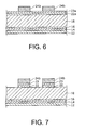
- an i-type amorphous silicon layer 32a and a p-type amorphous silicon layer 33a are formed to cover the insulating layer 24b, the i-type amorphous silicon layer 22, the n-type amorphous silicon layer 23, and the exposed back surface of the n-type monocrystalline silicon substrate 18 (S8) .
- the i-type amorphous silicon layer 32a and the p-type amorphous silicon layer 33a may be formed, for example, through plasma CVD.
- a portion of a part positioned over the insulating layer 24b is etched (S9) .
- an i-type amorphous silicon layer 32b and a p-type amorphous silicon layer 33b are formed.
- an alkaline etching solution such as an aqueous solution including sodium hydroxide (NaOH) is used.
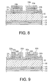
- the insulating layer 24b is etched to further remove a part of the insulating layer 24b (S10). Specifically, using the i-type amorphous silicon layer 32b and the p-type amorphous silicon layer 33b as a mask, the exposed part of the insulating layer 24b is etched and removed, to form the insulating layer 24. In this process, for the etching of the insulating layer 24b, for example, an acidic etching solution such as an aqueous solution of HF is used.
- a transparent conductive layer 26a and a metal layer 27a are formed (S11) .
- the transparent conductive layer 26a and the metal layer 27a are formed through a thin film formation method such as plasma CVD or sputtering.
- the transparent conductive layer 26a and the metal layer 27a a part positioned over the insulating layer 24 is partitioned, to form the transparent conductive layers 26 and 36 and the metal layers 27 and 37 (S12).
- the transparent conductive layer 26a and the metal layer 27a are partitioned, for example, through etching using a resist mask.
- the first electrode section 28 and the second electrode section 29 are sequentially formed over the metal layer 27, and the first electrode section 38 and the second electrode section 39 are sequentially formed over the metal layer 37 (S13) .
- the n-side electrode section 25 and the p-side electrode section 35 are formed.
- an interface between the n-type monocrystalline silicon substrate 18 and the i-type amorphous silicon layer 16 and an interface between the n-type monocrystalline silicon substrate 18 and the i-type amorphous silicon layers 22 and 32 are preferably maintained clean. Due to a difference in the degree of vacuum during film formation and wrap-around of the material gas, or the like, the degree of contamination on the surface opposite the surface on which the film is formed is greater during the film formation of the reflection prevention layer 12 and the insulating layer 24 than during the film formation of the i-type amorphous silicon films 22 and 32.
- the reflection prevention layer 12 and the insulating layer 24 are formed after the i-type amorphous silicon layer 16 and the n-type amorphous silicon layer 14 are formed over the light-receiving surface of the n-type monocrystalline silicon substrate 18 and the i-type amorphous silicon layer 22 and the n-type amorphous silicon layer 23 are formed over the back surface, so that the reflection prevention layer 12 and the insulating layer 24 are formed after both surfaces of the n-type monocrystalline silicon substrate 18 are covered at least with the i-type amorphous silicon layers 16 and 22.
- the i-type amorphous silicon layers 16, 22, and 32 can preferably function as passivation layers, and the power generation characteristic of the photovoltaic element 10 can be improved.
- the insulating layer 24 positioned on the back surface side is formed before the reflection prevention layer 12 positioned on the light-receiving surface side is formed. That is, the insulating layer 24 is formed to cover the n-type amorphous silicon layer 23, and to consequently prevent wrap-around of the material gas to a region over the n-type amorphous silicon layer 23 when the reflection prevention layer 12 is later formed.
- the surface of the n-type amorphous silicon layer 23 which is in contact with the n-side electrode section 25 which directly contributes to the collection of carriers can be maintained clean, and the contact resistance with the n-side electrode section 25 can be reduced. Therefore, the electricity collection efficiency in the n-side electrode section 25 can be improved and the power generation characteristic of the photovoltaic element 10 can be improved.
- the insulating layer 24a has a higher mechanical strength compared to the n-type amorphous silicon layer 23a.
- the insulating layer 24a By covering the region over the n-type amorphous silicon layer 23a with the insulating layer 24a, it is possible to inhibit damaging of the surface of the n-type amorphous silicon layer 23a during the production steps of the photovoltaic element 10, to improve electrical contact with the n-side electrode section 25, and to reduce the contact resistance. Therefore, the electricity collection efficiency at the n-side electrode section 25 can be improved and the power generation characteristic of the photovoltaic element 10 can be improved.
Landscapes
- Photovoltaic Devices (AREA)
- Life Sciences & Earth Sciences (AREA)
- Engineering & Computer Science (AREA)
- Sustainable Energy (AREA)
- Sustainable Development (AREA)
Applications Claiming Priority (2)
| Application Number | Priority Date | Filing Date | Title |
|---|---|---|---|
| JP2011067625 | 2011-03-25 | ||
| PCT/JP2012/057006 WO2012132995A1 (fr) | 2011-03-25 | 2012-03-19 | Procédé de fabrication d'un élément de conversion photoélectrique |
Publications (2)
| Publication Number | Publication Date |
|---|---|
| EP2690666A1 true EP2690666A1 (fr) | 2014-01-29 |
| EP2690666A4 EP2690666A4 (fr) | 2014-09-03 |
Family
ID=46930727
Family Applications (1)
| Application Number | Title | Priority Date | Filing Date |
|---|---|---|---|
| EP12763547.2A Ceased EP2690666A4 (fr) | 2011-03-25 | 2012-03-19 | Procédé de fabrication d'un élément de conversion photoélectrique |
Country Status (4)
| Country | Link |
|---|---|
| US (1) | US9257593B2 (fr) |
| EP (1) | EP2690666A4 (fr) |
| JP (1) | JP5891382B2 (fr) |
| WO (1) | WO2012132995A1 (fr) |
Cited By (1)
| Publication number | Priority date | Publication date | Assignee | Title |
|---|---|---|---|---|
| CN114342079A (zh) * | 2019-08-30 | 2022-04-12 | 株式会社日本显示器 | 检测装置 |
Families Citing this family (12)
| Publication number | Priority date | Publication date | Assignee | Title |
|---|---|---|---|---|
| US8597970B2 (en) | 2011-12-21 | 2013-12-03 | Sunpower Corporation | Hybrid polysilicon heterojunction back contact cell |
| JP6179900B2 (ja) * | 2012-03-30 | 2017-08-16 | パナソニックIpマネジメント株式会社 | 太陽電池及びその製造方法 |
| US9312406B2 (en) | 2012-12-19 | 2016-04-12 | Sunpower Corporation | Hybrid emitter all back contact solar cell |
| US9196758B2 (en) | 2013-12-20 | 2015-11-24 | Sunpower Corporation | Solar cell emitter region fabrication with differentiated p-type and n-type region architectures |
| JP6311968B2 (ja) * | 2014-03-14 | 2018-04-18 | パナソニックIpマネジメント株式会社 | 太陽電池 |
| US9825191B2 (en) * | 2014-06-27 | 2017-11-21 | Sunpower Corporation | Passivation of light-receiving surfaces of solar cells with high energy gap (EG) materials |
| US9837576B2 (en) | 2014-09-19 | 2017-12-05 | Sunpower Corporation | Solar cell emitter region fabrication with differentiated P-type and N-type architectures and incorporating dotted diffusion |
| US9525083B2 (en) | 2015-03-27 | 2016-12-20 | Sunpower Corporation | Solar cell emitter region fabrication with differentiated P-type and N-type architectures and incorporating a multi-purpose passivation and contact layer |
| US11355657B2 (en) | 2015-03-27 | 2022-06-07 | Sunpower Corporation | Metallization of solar cells with differentiated p-type and n-type region architectures |
| US9502601B1 (en) | 2016-04-01 | 2016-11-22 | Sunpower Corporation | Metallization of solar cells with differentiated P-type and N-type region architectures |
| JP6583753B2 (ja) * | 2018-03-08 | 2019-10-02 | パナソニックIpマネジメント株式会社 | 太陽電池 |
| JP2021044384A (ja) * | 2019-09-11 | 2021-03-18 | パナソニック株式会社 | 太陽電池セル |
Family Cites Families (14)
| Publication number | Priority date | Publication date | Assignee | Title |
|---|---|---|---|---|
| JPH0613639A (ja) * | 1992-06-24 | 1994-01-21 | Sanyo Electric Co Ltd | 光起電力装置 |
| JP2003298078A (ja) * | 2002-03-29 | 2003-10-17 | Ebara Corp | 光起電力素子 |
| US20070169808A1 (en) * | 2006-01-26 | 2007-07-26 | Kherani Nazir P | Solar cell |
| NO20061668L (no) * | 2006-04-12 | 2007-10-15 | Renewable Energy Corp | Solcelle og fremgangsmate for fremstilling av samme |
| KR20100015622A (ko) * | 2007-03-16 | 2010-02-12 | 비피 코포레이션 노쓰 아메리카 인코포레이티드 | 태양 전지 |
| JP5230222B2 (ja) | 2008-02-21 | 2013-07-10 | 三洋電機株式会社 | 太陽電池 |
| TWI478359B (zh) * | 2008-09-05 | 2015-03-21 | 半導體能源研究所股份有限公司 | 光電轉換裝置 |
| JP2010258043A (ja) * | 2009-04-21 | 2010-11-11 | Sanyo Electric Co Ltd | 太陽電池 |
| WO2011005447A2 (fr) * | 2009-06-22 | 2011-01-13 | International Business Machines Corporation | Structure de détecteur optique à semi-conducteur |
| US7927910B2 (en) * | 2009-06-28 | 2011-04-19 | Sino-American Silicon Products Inc. | Manufacturing method of solar cell |
| JP2011035092A (ja) * | 2009-07-31 | 2011-02-17 | Sanyo Electric Co Ltd | 裏面接合型太陽電池及びそれを用いた太陽電池モジュール |
| CN102044579B (zh) * | 2009-09-07 | 2013-12-18 | Lg电子株式会社 | 太阳能电池 |
| FR2953999B1 (fr) * | 2009-12-14 | 2012-01-20 | Total Sa | Cellule photovoltaique heterojonction a contact arriere |
| EP2690668A4 (fr) * | 2011-03-25 | 2014-09-03 | Sanyo Electric Co | Procédé de production d'un élément de conversion photoélectrique |
-
2012
- 2012-03-19 EP EP12763547.2A patent/EP2690666A4/fr not_active Ceased
- 2012-03-19 WO PCT/JP2012/057006 patent/WO2012132995A1/fr not_active Ceased
- 2012-03-19 JP JP2013507402A patent/JP5891382B2/ja not_active Expired - Fee Related
-
2013
- 2013-09-17 US US14/029,367 patent/US9257593B2/en not_active Expired - Fee Related
Cited By (1)
| Publication number | Priority date | Publication date | Assignee | Title |
|---|---|---|---|---|
| CN114342079A (zh) * | 2019-08-30 | 2022-04-12 | 株式会社日本显示器 | 检测装置 |
Also Published As
| Publication number | Publication date |
|---|---|
| US20140017850A1 (en) | 2014-01-16 |
| JPWO2012132995A1 (ja) | 2014-07-28 |
| US9257593B2 (en) | 2016-02-09 |
| EP2690666A4 (fr) | 2014-09-03 |
| JP5891382B2 (ja) | 2016-03-23 |
| WO2012132995A1 (fr) | 2012-10-04 |
Similar Documents
| Publication | Publication Date | Title |
|---|---|---|
| US9257593B2 (en) | Method for producing photoelectric conversion element | |
| JP5705968B2 (ja) | 光電変換装置及びその製造方法 | |
| EP2434548B1 (fr) | Cellule solaire et son procédé de fabrication | |
| EP2219222B1 (fr) | Cellule solaire et son procédé de fabrication | |
| JP5879538B2 (ja) | 光電変換装置及びその製造方法 | |
| KR101661768B1 (ko) | 태양전지 및 이의 제조 방법 | |
| EP2693488A1 (fr) | Dispositif de conversion photoélectrique et son procédé de production | |
| EP2479794A1 (fr) | Cellule solaire | |
| CN108140680B (zh) | 光电转换装置及其制造方法 | |
| KR101985835B1 (ko) | 광기전력소자 및 제조 방법 | |
| US20180069144A1 (en) | Solar cell and method for manufacturing same | |
| KR20130058497A (ko) | 태양전지 및 그 제조 방법 | |
| CN110010720A (zh) | 太阳能单电池的制造方法和太阳能单电池 | |
| JPWO2013094233A1 (ja) | 太陽電池の製造方法 | |
| KR20130067208A (ko) | 광기전력소자 및 그 제조 방법 | |
| EP2849233A1 (fr) | Cellule solaire | |
| CN111834475A (zh) | 太阳能单电池和太阳能电池组件 | |
| US20140024168A1 (en) | Method for producing photoelectric conversion device | |
| US9070822B2 (en) | Method for producing photoelectric conversion element | |
| US20170012164A1 (en) | Method of forming electrode pattern and method of manufacturing solar cell | |
| CN110098266A (zh) | 太阳能单电池和太阳能单电池的制造方法 | |
| WO2012132614A1 (fr) | Dispositif de conversion photoélectrique | |
| WO2012132064A1 (fr) | Élément photovoltaïque | |
| WO2012132616A1 (fr) | Procédé de fabrication d'un élément de conversion photoélectrique |
Legal Events
| Date | Code | Title | Description |
|---|---|---|---|
| PUAI | Public reference made under article 153(3) epc to a published international application that has entered the european phase |
Free format text: ORIGINAL CODE: 0009012 |
|
| 17P | Request for examination filed |
Effective date: 20130911 |
|
| AK | Designated contracting states |
Kind code of ref document: A1 Designated state(s): AL AT BE BG CH CY CZ DE DK EE ES FI FR GB GR HR HU IE IS IT LI LT LU LV MC MK MT NL NO PL PT RO RS SE SI SK SM TR |
|
| DAX | Request for extension of the european patent (deleted) | ||
| A4 | Supplementary search report drawn up and despatched |
Effective date: 20140806 |
|
| RIC1 | Information provided on ipc code assigned before grant |
Ipc: H01L 31/20 20060101ALI20140731BHEP Ipc: H01L 31/0352 20060101ALI20140731BHEP Ipc: H01L 31/0747 20120101ALI20140731BHEP Ipc: H01L 31/0216 20140101ALI20140731BHEP Ipc: H01L 31/068 20120101ALI20140731BHEP Ipc: H01L 31/0224 20060101ALI20140731BHEP Ipc: H01L 31/04 20140101AFI20140731BHEP |
|
| RAP1 | Party data changed (applicant data changed or rights of an application transferred) |
Owner name: PANASONIC INTELLECTUAL PROPERTY MANAGEMENT CO., LT |
|
| STAA | Information on the status of an ep patent application or granted ep patent |
Free format text: STATUS: EXAMINATION IS IN PROGRESS |
|
| 17Q | First examination report despatched |
Effective date: 20161219 |
|
| STAA | Information on the status of an ep patent application or granted ep patent |
Free format text: STATUS: THE APPLICATION HAS BEEN REFUSED |
|
| REG | Reference to a national code |
Ref country code: DE Ref legal event code: R003 |
|
| 18R | Application refused |
Effective date: 20180819 |