EP2693202B1 - Procédé de fabrication d'un dispositif destiné à améliorer un champ optoélectrique - Google Patents
Procédé de fabrication d'un dispositif destiné à améliorer un champ optoélectrique Download PDFInfo
- Publication number
- EP2693202B1 EP2693202B1 EP12764916.8A EP12764916A EP2693202B1 EP 2693202 B1 EP2693202 B1 EP 2693202B1 EP 12764916 A EP12764916 A EP 12764916A EP 2693202 B1 EP2693202 B1 EP 2693202B1
- Authority
- EP
- European Patent Office
- Prior art keywords
- recesses
- metal
- protrusions
- structure layer
- fine protrusions
- Prior art date
- Legal status (The legal status is an assumption and is not a legal conclusion. Google has not performed a legal analysis and makes no representation as to the accuracy of the status listed.)
- Not-in-force
Links
- 238000004519 manufacturing process Methods 0.000 title claims description 15
- 229910052751 metal Inorganic materials 0.000 claims description 99
- 239000002184 metal Substances 0.000 claims description 99
- 239000000758 substrate Substances 0.000 claims description 68
- 230000005684 electric field Effects 0.000 claims description 43
- 230000003287 optical effect Effects 0.000 claims description 43
- 230000002708 enhancing effect Effects 0.000 claims description 37
- 239000010408 film Substances 0.000 claims description 36
- 239000010931 gold Substances 0.000 claims description 34
- 229910052709 silver Inorganic materials 0.000 claims description 28
- BQCADISMDOOEFD-UHFFFAOYSA-N Silver Chemical compound [Ag] BQCADISMDOOEFD-UHFFFAOYSA-N 0.000 claims description 27
- 239000004332 silver Substances 0.000 claims description 27
- 229910052737 gold Inorganic materials 0.000 claims description 23
- 229910052782 aluminium Inorganic materials 0.000 claims description 22
- XAGFODPZIPBFFR-UHFFFAOYSA-N aluminium Chemical compound [Al] XAGFODPZIPBFFR-UHFFFAOYSA-N 0.000 claims description 22
- PCHJSUWPFVWCPO-UHFFFAOYSA-N gold Chemical compound [Au] PCHJSUWPFVWCPO-UHFFFAOYSA-N 0.000 claims description 22
- 238000000034 method Methods 0.000 claims description 16
- 229910001593 boehmite Inorganic materials 0.000 claims description 15
- FAHBNUUHRFUEAI-UHFFFAOYSA-M hydroxidooxidoaluminium Chemical compound O[Al]=O FAHBNUUHRFUEAI-UHFFFAOYSA-M 0.000 claims description 15
- 230000005284 excitation Effects 0.000 claims description 12
- 238000007740 vapor deposition Methods 0.000 claims description 11
- 239000004411 aluminium Substances 0.000 claims description 9
- PNEYBMLMFCGWSK-UHFFFAOYSA-N aluminium oxide Inorganic materials [O-2].[O-2].[O-2].[Al+3].[Al+3] PNEYBMLMFCGWSK-UHFFFAOYSA-N 0.000 claims description 9
- 229910001680 bayerite Inorganic materials 0.000 claims description 8
- 238000001027 hydrothermal synthesis Methods 0.000 claims description 8
- 239000010409 thin film Substances 0.000 claims description 8
- BASFCYQUMIYNBI-UHFFFAOYSA-N platinum Chemical compound [Pt] BASFCYQUMIYNBI-UHFFFAOYSA-N 0.000 claims description 7
- 238000010030 laminating Methods 0.000 claims description 5
- 239000010949 copper Substances 0.000 claims description 4
- 230000008021 deposition Effects 0.000 claims description 4
- RYGMFSIKBFXOCR-UHFFFAOYSA-N Copper Chemical compound [Cu] RYGMFSIKBFXOCR-UHFFFAOYSA-N 0.000 claims description 3
- 229910052802 copper Inorganic materials 0.000 claims description 3
- 229910052697 platinum Inorganic materials 0.000 claims description 3
- 238000001069 Raman spectroscopy Methods 0.000 description 24
- 238000001878 scanning electron micrograph Methods 0.000 description 16
- 239000011521 glass Substances 0.000 description 10
- 238000001237 Raman spectrum Methods 0.000 description 7
- 239000008187 granular material Substances 0.000 description 7
- OKKJLVBELUTLKV-UHFFFAOYSA-N Methanol Chemical compound OC OKKJLVBELUTLKV-UHFFFAOYSA-N 0.000 description 6
- 238000009835 boiling Methods 0.000 description 6
- 238000009826 distribution Methods 0.000 description 6
- XLYOFNOQVPJJNP-UHFFFAOYSA-N water Substances O XLYOFNOQVPJJNP-UHFFFAOYSA-N 0.000 description 5
- CSCPPACGZOOCGX-UHFFFAOYSA-N Acetone Chemical compound CC(C)=O CSCPPACGZOOCGX-UHFFFAOYSA-N 0.000 description 4
- 238000000151 deposition Methods 0.000 description 4
- 150000002739 metals Chemical class 0.000 description 4
- 238000001228 spectrum Methods 0.000 description 4
- 238000004416 surface enhanced Raman spectroscopy Methods 0.000 description 4
- 238000005259 measurement Methods 0.000 description 3
- 229910044991 metal oxide Inorganic materials 0.000 description 3
- 150000004706 metal oxides Chemical class 0.000 description 3
- 238000007254 oxidation reaction Methods 0.000 description 3
- 238000004544 sputter deposition Methods 0.000 description 3
- 239000000126 substance Substances 0.000 description 3
- LFQSCWFLJHTTHZ-UHFFFAOYSA-N Ethanol Chemical compound CCO LFQSCWFLJHTTHZ-UHFFFAOYSA-N 0.000 description 2
- VYPSYNLAJGMNEJ-UHFFFAOYSA-N Silicium dioxide Chemical compound O=[Si]=O VYPSYNLAJGMNEJ-UHFFFAOYSA-N 0.000 description 2
- 230000001419 dependent effect Effects 0.000 description 2
- 238000010586 diagram Methods 0.000 description 2
- 230000000694 effects Effects 0.000 description 2
- 230000001939 inductive effect Effects 0.000 description 2
- 230000035945 sensitivity Effects 0.000 description 2
- 229910002706 AlOOH Inorganic materials 0.000 description 1
- 229910001111 Fine metal Inorganic materials 0.000 description 1
- XUIMIQQOPSSXEZ-UHFFFAOYSA-N Silicon Chemical compound [Si] XUIMIQQOPSSXEZ-UHFFFAOYSA-N 0.000 description 1
- RTAQQCXQSZGOHL-UHFFFAOYSA-N Titanium Chemical compound [Ti] RTAQQCXQSZGOHL-UHFFFAOYSA-N 0.000 description 1
- 238000005054 agglomeration Methods 0.000 description 1
- 230000002776 aggregation Effects 0.000 description 1
- 229910045601 alloy Inorganic materials 0.000 description 1
- 239000000956 alloy Substances 0.000 description 1
- 229910021502 aluminium hydroxide Inorganic materials 0.000 description 1
- WNROFYMDJYEPJX-UHFFFAOYSA-K aluminium hydroxide Chemical compound [OH-].[OH-].[OH-].[Al+3] WNROFYMDJYEPJX-UHFFFAOYSA-K 0.000 description 1
- 238000007743 anodising Methods 0.000 description 1
- VYXSBFYARXAAKO-WTKGSRSZSA-N chembl402140 Chemical compound Cl.C1=2C=C(C)C(NCC)=CC=2OC2=C\C(=N/CC)C(C)=CC2=C1C1=CC=CC=C1C(=O)OCC VYXSBFYARXAAKO-WTKGSRSZSA-N 0.000 description 1
- 229910052681 coesite Inorganic materials 0.000 description 1
- 238000004891 communication Methods 0.000 description 1
- 229910052906 cristobalite Inorganic materials 0.000 description 1
- 238000001514 detection method Methods 0.000 description 1
- 229940079593 drug Drugs 0.000 description 1
- 239000003814 drug Substances 0.000 description 1
- 238000005530 etching Methods 0.000 description 1
- 229910001679 gibbsite Inorganic materials 0.000 description 1
- 230000001678 irradiating effect Effects 0.000 description 1
- 230000001788 irregular Effects 0.000 description 1
- 239000007788 liquid Substances 0.000 description 1
- 230000000873 masking effect Effects 0.000 description 1
- 230000003647 oxidation Effects 0.000 description 1
- 238000000206 photolithography Methods 0.000 description 1
- 239000011148 porous material Substances 0.000 description 1
- 230000003405 preventing effect Effects 0.000 description 1
- 229910052710 silicon Inorganic materials 0.000 description 1
- 239000010703 silicon Substances 0.000 description 1
- 239000000377 silicon dioxide Substances 0.000 description 1
- 238000003980 solgel method Methods 0.000 description 1
- 229910052682 stishovite Inorganic materials 0.000 description 1
- 239000010936 titanium Substances 0.000 description 1
- 229910052719 titanium Inorganic materials 0.000 description 1
- 229910052905 tridymite Inorganic materials 0.000 description 1
Images



Classifications
-
- G—PHYSICS
- G01—MEASURING; TESTING
- G01N—INVESTIGATING OR ANALYSING MATERIALS BY DETERMINING THEIR CHEMICAL OR PHYSICAL PROPERTIES
- G01N21/00—Investigating or analysing materials by the use of optical means, i.e. using sub-millimetre waves, infrared, visible or ultraviolet light
- G01N21/62—Systems in which the material investigated is excited whereby it emits light or causes a change in wavelength of the incident light
- G01N21/63—Systems in which the material investigated is excited whereby it emits light or causes a change in wavelength of the incident light optically excited
- G01N21/65—Raman scattering
- G01N21/658—Raman scattering enhancement Raman, e.g. surface plasmons
-
- G—PHYSICS
- G01—MEASURING; TESTING
- G01J—MEASUREMENT OF INTENSITY, VELOCITY, SPECTRAL CONTENT, POLARISATION, PHASE OR PULSE CHARACTERISTICS OF INFRARED, VISIBLE OR ULTRAVIOLET LIGHT; COLORIMETRY; RADIATION PYROMETRY
- G01J3/00—Spectrometry; Spectrophotometry; Monochromators; Measuring colours
- G01J3/28—Investigating the spectrum
- G01J3/44—Raman spectrometry; Scattering spectrometry ; Fluorescence spectrometry
-
- C—CHEMISTRY; METALLURGY
- C03—GLASS; MINERAL OR SLAG WOOL
- C03C—CHEMICAL COMPOSITION OF GLASSES, GLAZES OR VITREOUS ENAMELS; SURFACE TREATMENT OF GLASS; SURFACE TREATMENT OF FIBRES OR FILAMENTS MADE FROM GLASS, MINERALS OR SLAGS; JOINING GLASS TO GLASS OR OTHER MATERIALS
- C03C17/00—Surface treatment of glass, not in the form of fibres or filaments, by coating
- C03C17/06—Surface treatment of glass, not in the form of fibres or filaments, by coating with metals
- C03C17/09—Surface treatment of glass, not in the form of fibres or filaments, by coating with metals by deposition from the vapour phase
-
- C—CHEMISTRY; METALLURGY
- C23—COATING METALLIC MATERIAL; COATING MATERIAL WITH METALLIC MATERIAL; CHEMICAL SURFACE TREATMENT; DIFFUSION TREATMENT OF METALLIC MATERIAL; COATING BY VACUUM EVAPORATION, BY SPUTTERING, BY ION IMPLANTATION OR BY CHEMICAL VAPOUR DEPOSITION, IN GENERAL; INHIBITING CORROSION OF METALLIC MATERIAL OR INCRUSTATION IN GENERAL
- C23C—COATING METALLIC MATERIAL; COATING MATERIAL WITH METALLIC MATERIAL; SURFACE TREATMENT OF METALLIC MATERIAL BY DIFFUSION INTO THE SURFACE, BY CHEMICAL CONVERSION OR SUBSTITUTION; COATING BY VACUUM EVAPORATION, BY SPUTTERING, BY ION IMPLANTATION OR BY CHEMICAL VAPOUR DEPOSITION, IN GENERAL
- C23C14/00—Coating by vacuum evaporation, by sputtering or by ion implantation of the coating forming material
- C23C14/06—Coating by vacuum evaporation, by sputtering or by ion implantation of the coating forming material characterised by the coating material
- C23C14/14—Metallic material, boron or silicon
- C23C14/18—Metallic material, boron or silicon on other inorganic substrates
-
- C—CHEMISTRY; METALLURGY
- C23—COATING METALLIC MATERIAL; COATING MATERIAL WITH METALLIC MATERIAL; CHEMICAL SURFACE TREATMENT; DIFFUSION TREATMENT OF METALLIC MATERIAL; COATING BY VACUUM EVAPORATION, BY SPUTTERING, BY ION IMPLANTATION OR BY CHEMICAL VAPOUR DEPOSITION, IN GENERAL; INHIBITING CORROSION OF METALLIC MATERIAL OR INCRUSTATION IN GENERAL
- C23C—COATING METALLIC MATERIAL; COATING MATERIAL WITH METALLIC MATERIAL; SURFACE TREATMENT OF METALLIC MATERIAL BY DIFFUSION INTO THE SURFACE, BY CHEMICAL CONVERSION OR SUBSTITUTION; COATING BY VACUUM EVAPORATION, BY SPUTTERING, BY ION IMPLANTATION OR BY CHEMICAL VAPOUR DEPOSITION, IN GENERAL
- C23C14/00—Coating by vacuum evaporation, by sputtering or by ion implantation of the coating forming material
- C23C14/58—After-treatment
- C23C14/5846—Reactive treatment
- C23C14/5853—Oxidation
-
- C—CHEMISTRY; METALLURGY
- C23—COATING METALLIC MATERIAL; COATING MATERIAL WITH METALLIC MATERIAL; CHEMICAL SURFACE TREATMENT; DIFFUSION TREATMENT OF METALLIC MATERIAL; COATING BY VACUUM EVAPORATION, BY SPUTTERING, BY ION IMPLANTATION OR BY CHEMICAL VAPOUR DEPOSITION, IN GENERAL; INHIBITING CORROSION OF METALLIC MATERIAL OR INCRUSTATION IN GENERAL
- C23C—COATING METALLIC MATERIAL; COATING MATERIAL WITH METALLIC MATERIAL; SURFACE TREATMENT OF METALLIC MATERIAL BY DIFFUSION INTO THE SURFACE, BY CHEMICAL CONVERSION OR SUBSTITUTION; COATING BY VACUUM EVAPORATION, BY SPUTTERING, BY ION IMPLANTATION OR BY CHEMICAL VAPOUR DEPOSITION, IN GENERAL
- C23C28/00—Coating for obtaining at least two superposed coatings either by methods not provided for in a single one of groups C23C2/00 - C23C26/00 or by combinations of methods provided for in subclasses C23C and C25C or C25D
- C23C28/30—Coatings combining at least one metallic layer and at least one inorganic non-metallic layer
- C23C28/32—Coatings combining at least one metallic layer and at least one inorganic non-metallic layer including at least one pure metallic layer
- C23C28/322—Coatings combining at least one metallic layer and at least one inorganic non-metallic layer including at least one pure metallic layer only coatings of metal elements only
-
- C—CHEMISTRY; METALLURGY
- C23—COATING METALLIC MATERIAL; COATING MATERIAL WITH METALLIC MATERIAL; CHEMICAL SURFACE TREATMENT; DIFFUSION TREATMENT OF METALLIC MATERIAL; COATING BY VACUUM EVAPORATION, BY SPUTTERING, BY ION IMPLANTATION OR BY CHEMICAL VAPOUR DEPOSITION, IN GENERAL; INHIBITING CORROSION OF METALLIC MATERIAL OR INCRUSTATION IN GENERAL
- C23C—COATING METALLIC MATERIAL; COATING MATERIAL WITH METALLIC MATERIAL; SURFACE TREATMENT OF METALLIC MATERIAL BY DIFFUSION INTO THE SURFACE, BY CHEMICAL CONVERSION OR SUBSTITUTION; COATING BY VACUUM EVAPORATION, BY SPUTTERING, BY ION IMPLANTATION OR BY CHEMICAL VAPOUR DEPOSITION, IN GENERAL
- C23C28/00—Coating for obtaining at least two superposed coatings either by methods not provided for in a single one of groups C23C2/00 - C23C26/00 or by combinations of methods provided for in subclasses C23C and C25C or C25D
- C23C28/30—Coatings combining at least one metallic layer and at least one inorganic non-metallic layer
- C23C28/34—Coatings combining at least one metallic layer and at least one inorganic non-metallic layer including at least one inorganic non-metallic material layer, e.g. metal carbide, nitride, boride, silicide layer and their mixtures, enamels, phosphates and sulphates
- C23C28/345—Coatings combining at least one metallic layer and at least one inorganic non-metallic layer including at least one inorganic non-metallic material layer, e.g. metal carbide, nitride, boride, silicide layer and their mixtures, enamels, phosphates and sulphates with at least one oxide layer
-
- B—PERFORMING OPERATIONS; TRANSPORTING
- B82—NANOTECHNOLOGY
- B82Y—SPECIFIC USES OR APPLICATIONS OF NANOSTRUCTURES; MEASUREMENT OR ANALYSIS OF NANOSTRUCTURES; MANUFACTURE OR TREATMENT OF NANOSTRUCTURES
- B82Y20/00—Nanooptics, e.g. quantum optics or photonic crystals
-
- B—PERFORMING OPERATIONS; TRANSPORTING
- B82—NANOTECHNOLOGY
- B82Y—SPECIFIC USES OR APPLICATIONS OF NANOSTRUCTURES; MEASUREMENT OR ANALYSIS OF NANOSTRUCTURES; MANUFACTURE OR TREATMENT OF NANOSTRUCTURES
- B82Y40/00—Manufacture or treatment of nanostructures
-
- C—CHEMISTRY; METALLURGY
- C03—GLASS; MINERAL OR SLAG WOOL
- C03C—CHEMICAL COMPOSITION OF GLASSES, GLAZES OR VITREOUS ENAMELS; SURFACE TREATMENT OF GLASS; SURFACE TREATMENT OF FIBRES OR FILAMENTS MADE FROM GLASS, MINERALS OR SLAGS; JOINING GLASS TO GLASS OR OTHER MATERIALS
- C03C2218/00—Methods for coating glass
- C03C2218/30—Aspects of methods for coating glass not covered above
- C03C2218/32—After-treatment
Definitions
- the present invention is related to a method for producing an optical electrical field enhancing device equipped with a metal structure of fine protrusions and recesses capable of inducing localized Plasmon.
- Raman spectroscopy is a technique that obtains the spectrum of Raman scattered light (Raman spectrum) by spectrally analyzing scattered light obtained by irradiating a substance with a single wavelength light beam, and is utilized to identify substances.
- SERS Surface Enhanced Raman Scattering
- SERS utilizes the principle that when light is irradiated onto a metal body, particularly a metal body having nano order protrusions and recesses on the surface thereof, while the metal body is in contact with a substance, optical electrical field enhancement occurs due to localized plasmon resonance, and the intensity of Raman scattered light of a sample in contact with the surface of the metal body is amplified.
- Surface enhanced Raman scattering can be executed by employing a substrate having a metal structure of protrusions and recesses on the surface thereof as a carrier (substrate) that holds test subjects.
- Si substrates, on the surface of which protrusions and recesses are provided, having metal films formed on the surface having the protrusions and recesses, are mainly employed as substrates having metal structures of protrusions and recesses on the surfaces thereof (refer to Patent Documents 1 through 3).
- Non Patent Document 1 Optics Express, Vol. 17, No. 21, pp. 18556
- the metal structure of fine protrusions and recesses producing method is complex and it is difficult to form metal structures of fine protrusions and recesses having large areas in the inventions of Patent Documents 1 through 3 that employ photolithography and etching to form the structures of fine protrusions and recesses and the invention of Patent Document 4 that employs anodic oxidation to form the structures of fine protrusions and recesses. Therefore, it is considered that the cost of substrates per unit area is high. In addition, it is extremely difficult to form the aforementioned metal structures of fine protrusions and recesses on complex substrates such as liquid containers constituted by a plurality of protrusions and recesses.
- the present invention has been developed in view of the foregoing circumstances. It is an object of the present invention to provide method for producing an optical electrical field enhancing device on substrates having arbitrary shapes, over comparatively large areas, and at low cost.
- an optical electrical field enhancing device comprising:
- the metal structure layer has a different shape from the structure layer.
- the second metal is gold, silver, copper, aluminium or platinum.
- the second metal is gold and the thickness of the film formed by vapour deposition is 30 nm or greater.
- the second metal is preferably silver and the thickness of the film formed by vapour deposition is 150 nm or less.
- the method for producing an optical electrical field enhancing device of the present invention enables an optical electrical field enhancing device to be obtained with a metal structure layer of fine protrusions and recesses having sizes of the order of several tens of nanometers by the simple steps of: the thin film forming step that forms a thin film formed from aluminium (hereafter sometimes referred to as the first metal) or alumina on a substrate; the structure layer of fine protrusions and recesses forming step that forms a structure layer of fine protrusions and recesses from bayerite and/or boehmite, by causing the thin aluminium or alumina film formed on the substrate to undergo a hydrothermal reaction; and the metal layer forming step that forms the metal structure layer of fine protrusions and recesses constituted by a second metal on the surface of the structure layer of fine protrusions and recesses.
- each of the steps can be applied to substrates having comparatively large areas and substrates having arbitrary shapes. Therefore, it is possible to produce optical electrical field enhancing devices having large areas and optical electrical field enhancing devices having desired shapes.
- An optical electrical field enhancing device obtained by the production method of the present invention is capable of effectively inducing localized plasmon at the surface of the metal structure of fine protrusions and recesses when light is irradiated onto the fine metal protrusions and recesses on the surface thereof.
- the localized plasmon generates an optical electrical field enhancing effect.
- light generated by a test subject placed on the optical electrical field enhancing device when light is irradiated onto the region at which the test subject is placed will be amplified by the optical electrical field enhancing effect, and it becomes possible to detect the generated light at high sensitivity.
- the optical electrical field enhancing device can be favorably employed as a surface enhanced Raman substrate that effectively amplifies Raman signals, to achieve improvements in detection sensitivity.
- Figure 1 illustrates a method for producing an optical electrical field enhancing substrate, to form an optical electrical field enhancing device, and is a collection of sectional diagrams that illustrate each step of the method.
- a plank shaped transparent substrate main body 11 is prepared.
- the transparent substrate main body 11 is cleansed with acetone and methanol. Thereafter, aluminum is employed as a first metal, and an aluminum film 20 is formed on the surface of the transparent substrate main body 11 at a thickness of approximately several tens of nanometers by the sputtering method as a thin film forming step.
- the transparent substrate main body 11 having the aluminum film 20 thereon is immersed in boiling pure water then taken out after several minutes (approximately 5 minutes) as a structure layer of fine protrusions and recesses forming step.
- the boiling treatment (hydrothermal reaction) renders the aluminum film 20 transparent, and produces a transparent structure layer of fine protrusions and recesses 22 formed by bayerite or boehmite.
- a second metal is vapor deposited onto the structure layer of fine protrusions and recesses 22, as a metal layer forming step.
- a plank shaped substrate was employed in the example described above. However, the steps of the method may be applied to substrates of any desired shape.
- Aluminum is an example of the first metal that undergoes the hydrothermal reaction in the structure layer of fine protrusions and recesses forming step.
- a metal oxide such as alumina (Al(OH) 3 ) may be employed.
- a structure of fine protrusions and recesses having complex triangular pyramid structures (refer to Figure 3 ) formed of either or both of bayerite (Al[OH] 3 ) and boehmite (AlOOH) can be formed, by aluminum or alumina undergoing the hydrothermal reaction.
- the method for forming the thin film from aluminium or alumina onto the substrate 11 is not limited to the sputtering method.
- the film may alternatively be formed by the heated vapor deposition method or by the sol gel method.
- the hydrothermal reaction is not limited to the boiling process.
- the substrate on which the film of the first metal has been formed may be exposed to high temperature steam, to cause the first metal to react with the high temperature steam.
- the second metal that constitutes the metal structure layer of fine protrusions and recesses 24 may be any metal that generates localized plasmon when irradiated with excitation light.
- metals include: gold (Au), silver (Ag), copper (Cu), aluminum (Al), platinum (Pt), and alloys having these metals as their main components. Au and Ag are particularly preferable.
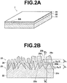
- Figure 2A is a perspective view that illustrates the optical electrical field enhancing substrate 1.
- Figure 2B is a magnified view of a portion IIB of the side surface of the optical electrical field enhancing substrate 1 illustrated in Figure 2A .
- the optical electrical field enhancing substrate 1 is constituted by the substrate 11, the structure layer of fine protrusions and recesses 22 having the structure of fine protrusions and recesses 23 on the surface thereof provided on the substrate 11, and the metal structure layer of fine protrusions and recesses 24 (metal layer) formed on the surface of the structure of fine protrusions and recesses 23.
- Localized plasmon resonance is induced by light (hereinafter, excitation light) irradiated onto a structure of fine protrusions and recesses 25 of the metal structure layer of fine protrusions and recesses 24, and an enhanced optical electrical field is generated on the surface of the metal structure layer of fine protrusions and recesses 24 by the localized plasmon resonance.
- the transparent structure of fine protrusions and recesses 23 formed by boehmite has an overall saw toothed cross section, although the sizes (the sizes of the peak angles) and orientations of the protrusions vary.
- the transparent structure of fine protrusions and recesses 23 is that on which the metal structure layer of fine protrusions and recesses 24 can be formed, and has an average pitch and an average depth which are less than the wavelength of the excitation light. Note that here, the pitch of the transparent structure of fine protrusions and recesses 23 is the distance among the peaks of adjacent protrusions having recesses therebetween, and the depth is the distance from the peaks of the protrusions to the bottoms of the recesses adjacent thereto.
- excitation light can be caused to enter from either the front surface or the back surface of the substrate to generate the optical electrical enhancing field at the surface of the metal layer 24.
- signal light such as Raman signal light can also be detected from either the front surface or the back surface of the substrate.
- transparent refers to a transmissivity of 50% or greater with respect to irradiated light and with respect to light generated by a test subject due to the irradiated light. Note that it is more preferable for the transmissivity with respect to these types of light to be 75% or greater, and even more preferably, 90% or greater.
- the metal structure layer of fine protrusions and recesses 24 is formed along the surface of the structure layer of fine protrusions and recesses 22, and may have substantially the same structure of fine protrusions and recesses as the structure of fine protrusions and recesses 23.
- the structure of fine protrusions and recesses 25 of the metal structure layer of fine protrusions and recesses 24 may have protrusions and recesses of shapes different from the structure of fine protrusions and recesses 23 of the structure layer of fine protrusions and recesses 22, as illustrated in Figure 2B .
- the structure of fine protrusions and recesses of the metal layer will have substantially the same structure of fine protrusions and recesses as the structure of fine protrusions and recesses 23 of the structure layer of fine protrusions and recesses 22. If the thickness of vapor deposited metal is thick, the metal structure layer of fine protrusions and recesses 24 will have a structure of fine protrusions and recesses in which the distances among adjacent protrusions is less than the distances among corresponding protrusions of the structure of fine protrusions and recesses 23, as illustrated in Figure 2B .
- Protrusions 24a of the metal structure layer of fine protrusions and recesses 24 are rounded, and the distances among adjacent protrusions are smaller compared to a case in which a metal film is formed along the structure of fine protrusions and recesses 23 of the structure layer of fine protrusions and recesses 22.
- portions at which the distance Wm between a protrusion 25a and an adjacent protrusion 25b in the structure of fine protrusions and recesses 25 of the metal structure layer of fine protrusions and recesses 24 is less than the distance Wb between a protrusion 23a and a protrusion 23b of the structure of fine protrusions and recesses 23 of the substrate corresponding to the protrusions 25a and 25b to be present, as illustrated in Figure 2B .
- the distance Wm between the adjacent protrusions 25a and 25b is defined as the distance from the peak of the lower protrusion 25b to a position of the protrusion 25a having half the depth Dm/2 of the depth Dm of the deepest portion of a recess 25c between the adjacent protrusions 25a and 25b.
- the distance Wb between the adjacent protrusions 23a and 23b is defined as the distance from the peak of the lower protrusion 23b to a position of the protrusion 23a having half the depth Db/2 of the depth Db of the deepest portion of a recess 23c between the adjacent protrusions 23a and 23b.
- the structure of fine protrusions and recesses 25 of the metal structure layer of fine protrusions and recesses 24 is a structure of fine protrusions and recesses in which at least one of the length of the protrusions in the direction perpendicular to the substrate and the length of the protrusions in the direction parallel to the substrate is less than the wavelength of excitation light, such that localized plasmon can be generated on the surface of the metal structure layer of fine protrusions and recesses 24.
- the protrusions of the metal structure layer of fine protrusions and recesses 24 prefferably be granules formed by agglomeration of metal. It is desirable for the aspect ratio (length in the direction perpendicular to the substrate/length in the direction parallel to the substrate) of the granular protrusions to be 0.5 or greater.
- the average depth from the peaks of the protrusions to the bottoms of recesses adjacent thereto is desirable for the average pitch among the peaks of adjacent protrusions having recesses therebetween to be 200nm or less in the structure of fine protrusions and recesses 25 of the metal structure layer of fine protrusions and recesses 24.
- the thickness of the metal structure layer of fine protrusions and recesses formed on the structure of fine protrusions and recesses of the substrate is 400 nm or less in the case that gold is used as the metal and for the thickness to be 90 nm or less in the case that silver is used as the metal.
- a metal structure of fine protrusions and recesses capable of generating an efficiently enhanced optical electrical field can be obtained, by vapor depositing amounts of gold or silver corresponding to these thicknesses.
- the distances among all adjacent protrusions in the structure of fine protrusions and recesses of the metal structure layer of fine protrusions and recesses it is not necessary for the distances among all adjacent protrusions in the structure of fine protrusions and recesses of the metal structure layer of fine protrusions and recesses to be less than the distances among corresponding adjacent protrusions in the structure of fine protrusions and recesses of the substrate.
- the optical electrical field enhancing effect will become more significant as the number of adjacent protrusions of the metal structure layer of fine protrusions and recesses having distances less than the distances of corresponding adjacent protrusions in the structure of fine protrusions and recesses of the substrate increases.
- a dielectric or a third metal different from the second metal is then laminated on the metal structure layer (24). Interference effects and oxidization preventing effects can be imparted by laminating two or more types of metals or by laminating a dielectric on the second metal.
- the oxidization of silver can be suppressed by providing a silver layer as the second metal, and by laminating gold on the silver layer.
- the thickness of the dielectric is to be 50nm or less.
- SiO 2 may be laminated at a thickness of 10nm on the metal structure layer of fine protrusions and recesses, for example.
- a glass substrate (BK-7: Eagle 2000 by Corning) was employed as the transparent substrate main body 11.
- the glass substrate main body 11 underwent ultrasonic cleansing (45kHz) with acetone for 5 minutes and with methanol for 5 minutes. Then, a 25nm thick layer of aluminum 20 was formed on the glass substrate 11 using a sputtering apparatus (by Canon Anelva) . Note that a surface shape measuring device (by TENCOR) was employed to measure the thickness of the aluminum layer, and the thickness was confirmed to be 25nm ( ⁇ 10%).
- Figure 3 illustrates the results of observing the surface of the boehmite layer 22 with a SEM (S4100 by Hitachi).
- the white portions of Figure 3 are protrusions, and the gray portions are recesses.
- the patterns of protrusions and recesses are irregular, but are formed across the entirety of the surfaces of the boehmite layer, and the in plane uniformity of the structure of fine protrusions and recesses is high. It can be understood that the structure of protrusions and recesses is constituted by a great number of peak shaped protrusions from the photograph of the surface of the boehmite layer illustrated in Figure 3 .
- Note that the cross section of the structure of protrusions and recesses of the boehmite layer is saw toothed as schematically illustrated in Figure 2B .
- the vapor deposited film thickness is measured by preparing glass substrates for measuring thickness separately from the samples, masking a portion of the surface of each glass substrate for measuring thickness, performing vapor deposition by placing the glass substrates for measuring thickness in a vapor deposition chamber with the substrates of the samples, removing the tape from the glass substrates for measuring thickness following vapor deposition, then measuring the thickness from surfaces where the tape is peeled off, on which metal has not been vapor deposited, to the surface of the vapor deposited metal.
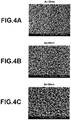
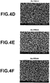
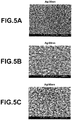
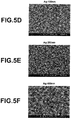
- the silver in the case of Ag vapor deposition, as the thickness of the silver formed by vapor deposition increases, the silver gradually at thicknesses from 30nm through 90nm to from island structures as illustrated in Figures 5A through 5C , and it is considered that the silver film layer gradually becomes flat. As illustrated in Figures 5D through 5F , the silver forms larger granular structures within thicknesses from 150nm through 400nm.
- Raman scattered light was detected employing a microscopic Raman spectroscope (HR800).
- HR800 Raman spectroscope
- a laser beam having a peak wavelength of 785nm was employed as the excitation light beam, and observation was performed at a magnification of 20x.
- the laser power was 0.5mW immediately after an objective lens, and the irradiation time was 10 seconds.
- Figure 6 and Figure 7 are graphs that illustrate Raman shift spectrum distributions detected by the microscopic Raman spectroscope.
- Figure 6 illustrates the Raman spectrum obtained for a sample onto which 60 ⁇ m of Au was vapor deposited
- Figure 7 illustrates the Raman spectrum obtained for a sample onto which 60 ⁇ m of Ag was vapor deposited.
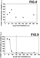
- Figure 8 is a graph that plots peak intensities of 1360cm -1 after removing white noise against Au vapor deposited film thickness as the horizontal axis, using Raman shift spectrum distributions obtained by detecting Raman scattered light at the front surfaces of the substrates for each of the samples on which Au was vapor deposited.
- the reason for the decrease in signal intensities is considered to be because the degree of optical electrical field enhancement deteriorates because the granule sizes increase, the granules contact each other, and become electrically continuous with each other.
- the signal intensity is greatest at the film thickness of 90nm. However, sufficient optical electrical enhancing effects are obtained at film thicknesses from 150nm through 400nm, and amplified Raman signals are detected.
- Figure 9 is a graph that plots peak intensities of 1360cm -1 after removing white noise against Ag vapor deposited film thickness as the horizontal axis, using Raman shift spectrum distributions obtained by detecting Raman scattered light at the front surfaces of the substrates for each of the samples on which Ag was vapor deposited.
- signal intensities decrease drastically when the film thickness becomes 150nm or greater and that substantially no signals are obtained in the case of silver.
- the reason for the decrease in signal intensities is considered to be because the degree of optical electrical field enhancement deteriorates because the granule sizes increase, the granules contact each other, and become electrically continuous with each other, as in the case of gold.
- the silver layer gradually becomes flat while the film thickness is relatively thin, then silver is further accumulated on the flattened silver layer. Therefore, it is considered that the silver layer readily becomes electrically continuous, resulting in the significant degrease in the optical electrical field intensity.
Landscapes
- Chemical & Material Sciences (AREA)
- Materials Engineering (AREA)
- Chemical Kinetics & Catalysis (AREA)
- Engineering & Computer Science (AREA)
- Organic Chemistry (AREA)
- Mechanical Engineering (AREA)
- Metallurgy (AREA)
- Inorganic Chemistry (AREA)
- Physics & Mathematics (AREA)
- Health & Medical Sciences (AREA)
- Life Sciences & Earth Sciences (AREA)
- Spectroscopy & Molecular Physics (AREA)
- General Physics & Mathematics (AREA)
- General Chemical & Material Sciences (AREA)
- Geochemistry & Mineralogy (AREA)
- Nuclear Medicine, Radiotherapy & Molecular Imaging (AREA)
- Analytical Chemistry (AREA)
- Biochemistry (AREA)
- General Health & Medical Sciences (AREA)
- Immunology (AREA)
- Pathology (AREA)
- Investigating, Analyzing Materials By Fluorescence Or Luminescence (AREA)
- Other Surface Treatments For Metallic Materials (AREA)
- Investigating Or Analysing Materials By Optical Means (AREA)
Claims (5)
- Procédé de fabrication d'un dispositif d'amélioration de champ optoélectrique (1) comprenant :la formation d'un film fin (20) à partir d'aluminium ou d'alumine sur un substrat (11) ;la formation d'une couche de structure (22) de saillies et évidements fins ayant un pas moyen et une profondeur moyenne qui sont inférieurs à la longueur d'onde de lumière d'excitation provenant de la bayerite et/ou de la boehmite en faisant subir au film fin d'aluminium ou d'alumine (20) une réaction hydrothermique, le pas étant la distance entre les pics de saillies adjacentes ayant des évidements entre elles, et la profondeur étant la distance depuis les pics des saillies jusqu'aux bas des évidements adjacents à celles-ci ;la formation d'une couche de structure métallique (24) de saillies et évidements fins constituée par un deuxième métal sur la surface de la couche de structure (22) de saillies et évidements fins par dépôt en phase vapeur, le deuxième métal étant capable de générer un plasmon localisé lorsqu'il est irradié par de la lumière d'excitation,la couche de structure métallique (24) étant telle qu'au moins une de la hauteur des saillies dans la direction perpendiculaire au substrat (11) et la longueur des saillies dans la direction parallèle au substrat (11) est inférieure à la longueur d'onde de lumière d'excitation ; etla stratification d'un métal diélectrique ou d'un troisième métal différent du deuxième métal sur la couche de structure métallique (24).
- Procédé selon la revendication 1, dans lequel la couche de structure métallique (24) a une forme différente de la couche de structure (22).
- Procédé selon la revendication 1 ou 2, dans lequel le deuxième métal est de l'or, de l'argent, du cuivre, de l'aluminium ou du platine.
- Procédé selon la revendication 3, dans lequel le deuxième métal est de l'or, et l'épaisseur du film formé par dépôt en phase vapeur est de 30 nm ou plus.
- Procédé selon la revendication 3, dans lequel le deuxième métal est de l'argent, et l'épaisseur du film formé par dépôt en phase vapeur est de 150 nm ou moins.
Applications Claiming Priority (2)
| Application Number | Priority Date | Filing Date | Title |
|---|---|---|---|
| JP2011077868A JP5801587B2 (ja) | 2011-03-31 | 2011-03-31 | 光電場増強デバイスの製造方法 |
| PCT/JP2012/002072 WO2012132385A1 (fr) | 2011-03-31 | 2012-03-26 | Procédé de fabrication d'un dispositif destiné à améliorer un champ optoélectrique |
Publications (3)
| Publication Number | Publication Date |
|---|---|
| EP2693202A1 EP2693202A1 (fr) | 2014-02-05 |
| EP2693202A4 EP2693202A4 (fr) | 2014-09-03 |
| EP2693202B1 true EP2693202B1 (fr) | 2017-11-15 |
Family
ID=46930161
Family Applications (1)
| Application Number | Title | Priority Date | Filing Date |
|---|---|---|---|
| EP12764916.8A Not-in-force EP2693202B1 (fr) | 2011-03-31 | 2012-03-26 | Procédé de fabrication d'un dispositif destiné à améliorer un champ optoélectrique |
Country Status (5)
| Country | Link |
|---|---|
| US (1) | US20140034235A1 (fr) |
| EP (1) | EP2693202B1 (fr) |
| JP (1) | JP5801587B2 (fr) |
| CN (1) | CN103492861B (fr) |
| WO (1) | WO2012132385A1 (fr) |
Families Citing this family (9)
| Publication number | Priority date | Publication date | Assignee | Title |
|---|---|---|---|---|
| JP6145861B2 (ja) | 2012-08-15 | 2017-06-14 | 富士フイルム株式会社 | 光電場増強デバイス、光測定装置および方法 |
| JP2014190834A (ja) * | 2013-03-27 | 2014-10-06 | Fujifilm Corp | 光電場増強デバイスおよびその製造方法 |
| JP6229387B2 (ja) * | 2013-09-12 | 2017-11-15 | 大日本印刷株式会社 | 光学部材、及びその製造方法 |
| JP6337127B2 (ja) * | 2014-08-27 | 2018-06-06 | 富士フイルム株式会社 | 光電場増強デバイスおよび光電場増強デバイスの製造方法 |
| CN105158228B (zh) * | 2015-07-30 | 2018-07-20 | 西北大学 | 基于勃姆石纳米薄膜的sers基底及制备方法 |
| CN109073642A (zh) | 2015-09-17 | 2018-12-21 | 格哈德·马勒 | 用于生物感测和其它应用的传感器设备 |
| CN106093007A (zh) * | 2016-06-20 | 2016-11-09 | 上海理工大学 | 一种表面增强拉曼散射基底及其制备方法 |
| CN108275651A (zh) * | 2018-01-22 | 2018-07-13 | 临沂大学 | 一种表面增强拉曼散射基底的制备方法 |
| FR3158725B1 (fr) * | 2024-01-31 | 2026-01-16 | Saint Gobain | Substrat de vitrage |
Citations (2)
| Publication number | Priority date | Publication date | Assignee | Title |
|---|---|---|---|---|
| EP2618133A1 (fr) * | 2010-09-17 | 2013-07-24 | FUJIFILM Corporation | Dispositif de renforcement de champ optique-électrique |
| EP2618134A1 (fr) * | 2010-09-17 | 2013-07-24 | FUJIFILM Corporation | Procédé de mesure de lumière et dispositif de mesure de lumière utilisant un dispositif d'amélioration de champ électro-optique |
Family Cites Families (16)
| Publication number | Priority date | Publication date | Assignee | Title |
|---|---|---|---|---|
| US4252843A (en) * | 1977-02-18 | 1981-02-24 | Minnesota Mining And Manufacturing Company | Process for forming a microstructured transmission and reflectance modifying coating |
| US4190321A (en) * | 1977-02-18 | 1980-02-26 | Minnesota Mining And Manufacturing Company | Microstructured transmission and reflectance modifying coating |
| JPH09202649A (ja) * | 1996-01-24 | 1997-08-05 | Central Glass Co Ltd | 花弁状透明アルミナ膜及びその形成法 |
| US6406777B1 (en) * | 2000-06-14 | 2002-06-18 | The United States Of America As Represented By The Secretary Of The Navy | Metal and glass structure for use in surface enhanced Raman spectroscopy and method for fabricating same |
| US7361313B2 (en) | 2003-02-18 | 2008-04-22 | Intel Corporation | Methods for uniform metal impregnation into a nanoporous material |
| US6970239B2 (en) | 2002-06-12 | 2005-11-29 | Intel Corporation | Metal coated nanocrystalline silicon as an active surface enhanced Raman spectroscopy (SERS) substrate |
| JP4163606B2 (ja) | 2003-12-10 | 2008-10-08 | 富士フイルム株式会社 | 微細構造体、微細構造体の作製方法、ラマン分光方法および装置 |
| JP2006145230A (ja) | 2004-11-16 | 2006-06-08 | Canon Inc | 被分析物担体およびその製造方法 |
| JP2007240361A (ja) * | 2006-03-09 | 2007-09-20 | Sekisui Chem Co Ltd | 局在プラズモン増強センサ |
| JP4639241B2 (ja) * | 2007-02-20 | 2011-02-23 | キヤノン株式会社 | 光学用部材、それを用いた光学系及び光学用部材の製造方法 |
| JP2009109395A (ja) * | 2007-10-31 | 2009-05-21 | Fujifilm Corp | 微細構造体の作製方法、微細構造体、ラマン分光用デバイス、ラマン分光装置、分析装置、検出装置、および質量分析装置 |
| JP2009236830A (ja) * | 2008-03-28 | 2009-10-15 | Sumitomo Precision Prod Co Ltd | 被分析物担体、及び、その製造方法 |
| JP5466226B2 (ja) * | 2009-03-04 | 2014-04-09 | 有限会社マイテック | 表面増強ラマン散乱活性測定基板 |
| US8427639B2 (en) * | 2009-05-07 | 2013-04-23 | Nant Holdings Ip, Llc | Surfaced enhanced Raman spectroscopy substrates |
| US20110128535A1 (en) * | 2009-11-30 | 2011-06-02 | David Eugene Baker | Nano-Structured Substrates, Articles, and Methods Thereof |
| JP2012132743A (ja) * | 2010-12-21 | 2012-07-12 | Fujifilm Corp | 光電場増強デバイスおよび光検出装置 |
-
2011
- 2011-03-31 JP JP2011077868A patent/JP5801587B2/ja not_active Expired - Fee Related
-
2012
- 2012-03-26 WO PCT/JP2012/002072 patent/WO2012132385A1/fr not_active Ceased
- 2012-03-26 EP EP12764916.8A patent/EP2693202B1/fr not_active Not-in-force
- 2012-03-26 CN CN201280016792.0A patent/CN103492861B/zh not_active Expired - Fee Related
-
2013
- 2013-09-30 US US14/041,877 patent/US20140034235A1/en not_active Abandoned
Patent Citations (2)
| Publication number | Priority date | Publication date | Assignee | Title |
|---|---|---|---|---|
| EP2618133A1 (fr) * | 2010-09-17 | 2013-07-24 | FUJIFILM Corporation | Dispositif de renforcement de champ optique-électrique |
| EP2618134A1 (fr) * | 2010-09-17 | 2013-07-24 | FUJIFILM Corporation | Procédé de mesure de lumière et dispositif de mesure de lumière utilisant un dispositif d'amélioration de champ électro-optique |
Also Published As
| Publication number | Publication date |
|---|---|
| WO2012132385A1 (fr) | 2012-10-04 |
| EP2693202A1 (fr) | 2014-02-05 |
| JP2012211839A (ja) | 2012-11-01 |
| CN103492861B (zh) | 2016-08-10 |
| US20140034235A1 (en) | 2014-02-06 |
| JP5801587B2 (ja) | 2015-10-28 |
| EP2693202A4 (fr) | 2014-09-03 |
| CN103492861A (zh) | 2014-01-01 |
Similar Documents
| Publication | Publication Date | Title |
|---|---|---|
| EP2693202A1 (fr) | Procédé de fabrication d'un dispositif destiné à améliorer un champ optoélectrique | |
| EP2690427B1 (fr) | Dispositif de renforcement de champ électrique optique et dispositif de mesure pourvu d'un tel dispositif | |
| EP2618133B1 (fr) | Dispositif de renforcement de champ optique-électrique | |
| EP2618134B1 (fr) | Procédé de mesure de lumière et dispositif de mesure de lumière utilisant un dispositif d'amélioration de champ électro-optique | |
| EP3966159A1 (fr) | Substrats de spectroscopie raman exaltée de surface et procédé de fabrication associé | |
| WO2009017846A1 (fr) | Substrats pour spectroscopie de raman amplifiée en surface à revêtements de métal discontinus | |
| Bechelany et al. | Extended domains of organized nanorings of silver grains as surface-enhanced Raman scattering sensors for molecular detection | |
| US10094956B2 (en) | Optical field enhancement device and manufacturing method of the same | |
| JP2004279364A (ja) | センサチップおよびセンサチップの製造方法並びにそのセンサチップを用いたセンサ | |
| JP2009103651A (ja) | 光電場増強デバイス、表面増強ラマン分光方法および表面増強ラマン分光装置 | |
| JP6337127B2 (ja) | 光電場増強デバイスおよび光電場増強デバイスの製造方法 | |
| JP2014016221A (ja) | 光電場増強デバイスおよびその製造方法 | |
| US9645087B2 (en) | Measuring apparatus where a distance between a surface of a transparent substrate on which a marker pattern is formed and a front surface is within a depth of focus of a detecting means | |
| JP7794472B2 (ja) | 表面増強ラマン散乱基板の製造方法 | |
| Hu et al. | Metal-coated Si nanograss as highly sensitive SERS sensors | |
| Bhatia et al. | Facile synthesis of graphene-coupled silver nanostructure-based hybrid SERS for trace-level SERS detection of thiram | |
| PL219899B1 (pl) | Sposób pokrywania hydrofilowych ciał stałych złotymi strukturami | |
| Dar et al. | Synthesis of Gold-Decorated Al Nanostructures as Platforms for SERS Detection | |
| PL224311B1 (pl) | Sposób otrzymywania platformy do badań substancji chemicznych techniką wzmocnionej powierzchniowo spektroskopii Ramana i otrzymana tym sposobem platforma | |
| UA90717U (uk) | СПОСІБ ОДЕРЖАННЯ ПЛІВКИ З Au НАНОЧАСТИНКАМИ ДЛЯ ПОВЕРХНЕВОГО ПІДСИЛЕННЯ КОМБІНАЦІЙНОГО РОЗСІЯННЯ СВІТЛА | |
| Adiguzel et al. | A Nanopatterned Silver–Polymer Platform for Ultrasensitive, Label-Free Diagnosis of Pancreatic Cancer |
Legal Events
| Date | Code | Title | Description |
|---|---|---|---|
| PUAI | Public reference made under article 153(3) epc to a published international application that has entered the european phase |
Free format text: ORIGINAL CODE: 0009012 |
|
| 17P | Request for examination filed |
Effective date: 20131023 |
|
| AK | Designated contracting states |
Kind code of ref document: A1 Designated state(s): AL AT BE BG CH CY CZ DE DK EE ES FI FR GB GR HR HU IE IS IT LI LT LU LV MC MK MT NL NO PL PT RO RS SE SI SK SM TR |
|
| DAX | Request for extension of the european patent (deleted) | ||
| A4 | Supplementary search report drawn up and despatched |
Effective date: 20140806 |
|
| RIC1 | Information provided on ipc code assigned before grant |
Ipc: B82Y 15/00 20110101ALI20140731BHEP Ipc: B82Y 20/00 20110101ALI20140731BHEP Ipc: G01N 21/65 20060101AFI20140731BHEP |
|
| 17Q | First examination report despatched |
Effective date: 20160616 |
|
| RIC1 | Information provided on ipc code assigned before grant |
Ipc: G01N 21/65 20060101AFI20170519BHEP Ipc: B82Y 40/00 20110101ALN20170519BHEP Ipc: B82Y 15/00 20110101ALN20170519BHEP Ipc: C23C 14/58 20060101ALI20170519BHEP Ipc: C23C 14/18 20060101ALI20170519BHEP Ipc: B82Y 20/00 20110101ALN20170519BHEP Ipc: C23C 28/00 20060101ALI20170519BHEP Ipc: C03C 17/09 20060101ALI20170519BHEP |
|
| GRAP | Despatch of communication of intention to grant a patent |
Free format text: ORIGINAL CODE: EPIDOSNIGR1 |
|
| INTG | Intention to grant announced |
Effective date: 20170707 |
|
| GRAS | Grant fee paid |
Free format text: ORIGINAL CODE: EPIDOSNIGR3 |
|
| GRAA | (expected) grant |
Free format text: ORIGINAL CODE: 0009210 |
|
| AK | Designated contracting states |
Kind code of ref document: B1 Designated state(s): AL AT BE BG CH CY CZ DE DK EE ES FI FR GB GR HR HU IE IS IT LI LT LU LV MC MK MT NL NO PL PT RO RS SE SI SK SM TR |
|
| REG | Reference to a national code |
Ref country code: CH Ref legal event code: EP Ref country code: GB Ref legal event code: FG4D Ref country code: AT Ref legal event code: REF Ref document number: 946766 Country of ref document: AT Kind code of ref document: T Effective date: 20171115 |
|
| REG | Reference to a national code |
Ref country code: IE Ref legal event code: FG4D |
|
| REG | Reference to a national code |
Ref country code: DE Ref legal event code: R096 Ref document number: 602012039842 Country of ref document: DE |
|
| REG | Reference to a national code |
Ref country code: NL Ref legal event code: MP Effective date: 20171115 |
|
| REG | Reference to a national code |
Ref country code: LT Ref legal event code: MG4D |
|
| REG | Reference to a national code |
Ref country code: AT Ref legal event code: MK05 Ref document number: 946766 Country of ref document: AT Kind code of ref document: T Effective date: 20171115 |
|
| PG25 | Lapsed in a contracting state [announced via postgrant information from national office to epo] |
Ref country code: LT Free format text: LAPSE BECAUSE OF FAILURE TO SUBMIT A TRANSLATION OF THE DESCRIPTION OR TO PAY THE FEE WITHIN THE PRESCRIBED TIME-LIMIT Effective date: 20171115 Ref country code: NO Free format text: LAPSE BECAUSE OF FAILURE TO SUBMIT A TRANSLATION OF THE DESCRIPTION OR TO PAY THE FEE WITHIN THE PRESCRIBED TIME-LIMIT Effective date: 20180215 Ref country code: NL Free format text: LAPSE BECAUSE OF FAILURE TO SUBMIT A TRANSLATION OF THE DESCRIPTION OR TO PAY THE FEE WITHIN THE PRESCRIBED TIME-LIMIT Effective date: 20171115 Ref country code: ES Free format text: LAPSE BECAUSE OF FAILURE TO SUBMIT A TRANSLATION OF THE DESCRIPTION OR TO PAY THE FEE WITHIN THE PRESCRIBED TIME-LIMIT Effective date: 20171115 Ref country code: FI Free format text: LAPSE BECAUSE OF FAILURE TO SUBMIT A TRANSLATION OF THE DESCRIPTION OR TO PAY THE FEE WITHIN THE PRESCRIBED TIME-LIMIT Effective date: 20171115 Ref country code: SE Free format text: LAPSE BECAUSE OF FAILURE TO SUBMIT A TRANSLATION OF THE DESCRIPTION OR TO PAY THE FEE WITHIN THE PRESCRIBED TIME-LIMIT Effective date: 20171115 |
|
| PG25 | Lapsed in a contracting state [announced via postgrant information from national office to epo] |
Ref country code: HR Free format text: LAPSE BECAUSE OF FAILURE TO SUBMIT A TRANSLATION OF THE DESCRIPTION OR TO PAY THE FEE WITHIN THE PRESCRIBED TIME-LIMIT Effective date: 20171115 Ref country code: RS Free format text: LAPSE BECAUSE OF FAILURE TO SUBMIT A TRANSLATION OF THE DESCRIPTION OR TO PAY THE FEE WITHIN THE PRESCRIBED TIME-LIMIT Effective date: 20171115 Ref country code: BG Free format text: LAPSE BECAUSE OF FAILURE TO SUBMIT A TRANSLATION OF THE DESCRIPTION OR TO PAY THE FEE WITHIN THE PRESCRIBED TIME-LIMIT Effective date: 20180215 Ref country code: LV Free format text: LAPSE BECAUSE OF FAILURE TO SUBMIT A TRANSLATION OF THE DESCRIPTION OR TO PAY THE FEE WITHIN THE PRESCRIBED TIME-LIMIT Effective date: 20171115 Ref country code: AT Free format text: LAPSE BECAUSE OF FAILURE TO SUBMIT A TRANSLATION OF THE DESCRIPTION OR TO PAY THE FEE WITHIN THE PRESCRIBED TIME-LIMIT Effective date: 20171115 Ref country code: GR Free format text: LAPSE BECAUSE OF FAILURE TO SUBMIT A TRANSLATION OF THE DESCRIPTION OR TO PAY THE FEE WITHIN THE PRESCRIBED TIME-LIMIT Effective date: 20180216 |
|
| PG25 | Lapsed in a contracting state [announced via postgrant information from national office to epo] |
Ref country code: CZ Free format text: LAPSE BECAUSE OF FAILURE TO SUBMIT A TRANSLATION OF THE DESCRIPTION OR TO PAY THE FEE WITHIN THE PRESCRIBED TIME-LIMIT Effective date: 20171115 Ref country code: CY Free format text: LAPSE BECAUSE OF FAILURE TO SUBMIT A TRANSLATION OF THE DESCRIPTION OR TO PAY THE FEE WITHIN THE PRESCRIBED TIME-LIMIT Effective date: 20171115 Ref country code: EE Free format text: LAPSE BECAUSE OF FAILURE TO SUBMIT A TRANSLATION OF THE DESCRIPTION OR TO PAY THE FEE WITHIN THE PRESCRIBED TIME-LIMIT Effective date: 20171115 Ref country code: DK Free format text: LAPSE BECAUSE OF FAILURE TO SUBMIT A TRANSLATION OF THE DESCRIPTION OR TO PAY THE FEE WITHIN THE PRESCRIBED TIME-LIMIT Effective date: 20171115 Ref country code: SK Free format text: LAPSE BECAUSE OF FAILURE TO SUBMIT A TRANSLATION OF THE DESCRIPTION OR TO PAY THE FEE WITHIN THE PRESCRIBED TIME-LIMIT Effective date: 20171115 |
|
| REG | Reference to a national code |
Ref country code: DE Ref legal event code: R097 Ref document number: 602012039842 Country of ref document: DE |
|
| PG25 | Lapsed in a contracting state [announced via postgrant information from national office to epo] |
Ref country code: IT Free format text: LAPSE BECAUSE OF FAILURE TO SUBMIT A TRANSLATION OF THE DESCRIPTION OR TO PAY THE FEE WITHIN THE PRESCRIBED TIME-LIMIT Effective date: 20171115 Ref country code: RO Free format text: LAPSE BECAUSE OF FAILURE TO SUBMIT A TRANSLATION OF THE DESCRIPTION OR TO PAY THE FEE WITHIN THE PRESCRIBED TIME-LIMIT Effective date: 20171115 Ref country code: PL Free format text: LAPSE BECAUSE OF FAILURE TO SUBMIT A TRANSLATION OF THE DESCRIPTION OR TO PAY THE FEE WITHIN THE PRESCRIBED TIME-LIMIT Effective date: 20171115 Ref country code: SM Free format text: LAPSE BECAUSE OF FAILURE TO SUBMIT A TRANSLATION OF THE DESCRIPTION OR TO PAY THE FEE WITHIN THE PRESCRIBED TIME-LIMIT Effective date: 20171115 |
|
| PLBE | No opposition filed within time limit |
Free format text: ORIGINAL CODE: 0009261 |
|
| STAA | Information on the status of an ep patent application or granted ep patent |
Free format text: STATUS: NO OPPOSITION FILED WITHIN TIME LIMIT |
|
| 26N | No opposition filed |
Effective date: 20180817 |
|
| REG | Reference to a national code |
Ref country code: CH Ref legal event code: PL |
|
| PG25 | Lapsed in a contracting state [announced via postgrant information from national office to epo] |
Ref country code: MC Free format text: LAPSE BECAUSE OF FAILURE TO SUBMIT A TRANSLATION OF THE DESCRIPTION OR TO PAY THE FEE WITHIN THE PRESCRIBED TIME-LIMIT Effective date: 20171115 Ref country code: SI Free format text: LAPSE BECAUSE OF FAILURE TO SUBMIT A TRANSLATION OF THE DESCRIPTION OR TO PAY THE FEE WITHIN THE PRESCRIBED TIME-LIMIT Effective date: 20171115 |
|
| REG | Reference to a national code |
Ref country code: BE Ref legal event code: MM Effective date: 20180331 |
|
| REG | Reference to a national code |
Ref country code: IE Ref legal event code: MM4A |
|
| PG25 | Lapsed in a contracting state [announced via postgrant information from national office to epo] |
Ref country code: LU Free format text: LAPSE BECAUSE OF NON-PAYMENT OF DUE FEES Effective date: 20180326 |
|
| PG25 | Lapsed in a contracting state [announced via postgrant information from national office to epo] |
Ref country code: IE Free format text: LAPSE BECAUSE OF NON-PAYMENT OF DUE FEES Effective date: 20180326 |
|
| PG25 | Lapsed in a contracting state [announced via postgrant information from national office to epo] |
Ref country code: CH Free format text: LAPSE BECAUSE OF NON-PAYMENT OF DUE FEES Effective date: 20180331 Ref country code: LI Free format text: LAPSE BECAUSE OF NON-PAYMENT OF DUE FEES Effective date: 20180331 Ref country code: BE Free format text: LAPSE BECAUSE OF NON-PAYMENT OF DUE FEES Effective date: 20180331 |
|
| PG25 | Lapsed in a contracting state [announced via postgrant information from national office to epo] |
Ref country code: FR Free format text: LAPSE BECAUSE OF NON-PAYMENT OF DUE FEES Effective date: 20180331 |
|
| PG25 | Lapsed in a contracting state [announced via postgrant information from national office to epo] |
Ref country code: MT Free format text: LAPSE BECAUSE OF NON-PAYMENT OF DUE FEES Effective date: 20180326 |
|
| PG25 | Lapsed in a contracting state [announced via postgrant information from national office to epo] |
Ref country code: TR Free format text: LAPSE BECAUSE OF FAILURE TO SUBMIT A TRANSLATION OF THE DESCRIPTION OR TO PAY THE FEE WITHIN THE PRESCRIBED TIME-LIMIT Effective date: 20171115 |
|
| PGFP | Annual fee paid to national office [announced via postgrant information from national office to epo] |
Ref country code: DE Payment date: 20200310 Year of fee payment: 9 Ref country code: GB Payment date: 20200318 Year of fee payment: 9 |
|
| PG25 | Lapsed in a contracting state [announced via postgrant information from national office to epo] |
Ref country code: PT Free format text: LAPSE BECAUSE OF FAILURE TO SUBMIT A TRANSLATION OF THE DESCRIPTION OR TO PAY THE FEE WITHIN THE PRESCRIBED TIME-LIMIT Effective date: 20171115 Ref country code: HU Free format text: LAPSE BECAUSE OF FAILURE TO SUBMIT A TRANSLATION OF THE DESCRIPTION OR TO PAY THE FEE WITHIN THE PRESCRIBED TIME-LIMIT; INVALID AB INITIO Effective date: 20120326 |
|
| PG25 | Lapsed in a contracting state [announced via postgrant information from national office to epo] |
Ref country code: MK Free format text: LAPSE BECAUSE OF NON-PAYMENT OF DUE FEES Effective date: 20171115 |
|
| PG25 | Lapsed in a contracting state [announced via postgrant information from national office to epo] |
Ref country code: AL Free format text: LAPSE BECAUSE OF FAILURE TO SUBMIT A TRANSLATION OF THE DESCRIPTION OR TO PAY THE FEE WITHIN THE PRESCRIBED TIME-LIMIT Effective date: 20171115 Ref country code: IS Free format text: LAPSE BECAUSE OF FAILURE TO SUBMIT A TRANSLATION OF THE DESCRIPTION OR TO PAY THE FEE WITHIN THE PRESCRIBED TIME-LIMIT Effective date: 20180315 |
|
| REG | Reference to a national code |
Ref country code: DE Ref legal event code: R119 Ref document number: 602012039842 Country of ref document: DE |
|
| GBPC | Gb: european patent ceased through non-payment of renewal fee |
Effective date: 20210326 |
|
| PG25 | Lapsed in a contracting state [announced via postgrant information from national office to epo] |
Ref country code: DE Free format text: LAPSE BECAUSE OF NON-PAYMENT OF DUE FEES Effective date: 20211001 Ref country code: GB Free format text: LAPSE BECAUSE OF NON-PAYMENT OF DUE FEES Effective date: 20210326 |