EP2696290A1 - Speicherschaltungssystem und -Verfahren - Google Patents
Speicherschaltungssystem und -Verfahren Download PDFInfo
- Publication number
- EP2696290A1 EP2696290A1 EP13191794.0A EP13191794A EP2696290A1 EP 2696290 A1 EP2696290 A1 EP 2696290A1 EP 13191794 A EP13191794 A EP 13191794A EP 2696290 A1 EP2696290 A1 EP 2696290A1
- Authority
- EP
- European Patent Office
- Prior art keywords
- memory
- dram
- circuits
- circuit
- integrated circuit
- Prior art date
- Legal status (The legal status is an assumption and is not a legal conclusion. Google has not performed a legal analysis and makes no representation as to the accuracy of the status listed.)
- Granted
Links
Images













Classifications
-
- G—PHYSICS
- G06—COMPUTING OR CALCULATING; COUNTING
- G06F—ELECTRIC DIGITAL DATA PROCESSING
- G06F12/00—Accessing, addressing or allocating within memory systems or architectures
-
- G—PHYSICS
- G06—COMPUTING OR CALCULATING; COUNTING
- G06F—ELECTRIC DIGITAL DATA PROCESSING
- G06F13/00—Interconnection of, or transfer of information or other signals between, memories, input/output devices or central processing units
- G06F13/14—Handling requests for interconnection or transfer
- G06F13/16—Handling requests for interconnection or transfer for access to memory bus
- G06F13/1668—Details of memory controller
- G06F13/1673—Details of memory controller using buffers
-
- G—PHYSICS
- G06—COMPUTING OR CALCULATING; COUNTING
- G06F—ELECTRIC DIGITAL DATA PROCESSING
- G06F13/00—Interconnection of, or transfer of information or other signals between, memories, input/output devices or central processing units
- G06F13/14—Handling requests for interconnection or transfer
- G06F13/16—Handling requests for interconnection or transfer for access to memory bus
-
- G—PHYSICS
- G06—COMPUTING OR CALCULATING; COUNTING
- G06F—ELECTRIC DIGITAL DATA PROCESSING
- G06F13/00—Interconnection of, or transfer of information or other signals between, memories, input/output devices or central processing units
- G06F13/14—Handling requests for interconnection or transfer
- G06F13/16—Handling requests for interconnection or transfer for access to memory bus
- G06F13/1605—Handling requests for interconnection or transfer for access to memory bus based on arbitration
- G06F13/1652—Handling requests for interconnection or transfer for access to memory bus based on arbitration in a multiprocessor architecture
- G06F13/1657—Access to multiple memories
-
- H—ELECTRICITY
- H10—SEMICONDUCTOR DEVICES; ELECTRIC SOLID-STATE DEVICES NOT OTHERWISE PROVIDED FOR
- H10W—GENERIC PACKAGES, INTERCONNECTIONS, CONNECTORS OR OTHER CONSTRUCTIONAL DETAILS OF DEVICES COVERED BY CLASS H10
- H10W90/00—Package configurations
-
- G—PHYSICS
- G11—INFORMATION STORAGE
- G11C—STATIC STORES
- G11C11/00—Digital stores characterised by the use of particular electric or magnetic storage elements; Storage elements therefor
- G11C11/21—Digital stores characterised by the use of particular electric or magnetic storage elements; Storage elements therefor using electric elements
- G11C11/34—Digital stores characterised by the use of particular electric or magnetic storage elements; Storage elements therefor using electric elements using semiconductor devices
- G11C11/40—Digital stores characterised by the use of particular electric or magnetic storage elements; Storage elements therefor using electric elements using semiconductor devices using transistors
- G11C11/401—Digital stores characterised by the use of particular electric or magnetic storage elements; Storage elements therefor using electric elements using semiconductor devices using transistors forming cells needing refreshing or charge regeneration, i.e. dynamic cells
- G11C11/406—Management or control of the refreshing or charge-regeneration cycles
- G11C11/40618—Refresh operations over multiple banks or interleaving
-
- G—PHYSICS
- G11—INFORMATION STORAGE
- G11C—STATIC STORES
- G11C7/00—Arrangements for writing information into, or reading information out from, a digital store
- G11C7/02—Arrangements for writing information into, or reading information out from, a digital store with means for avoiding parasitic signals
-
- H—ELECTRICITY
- H10—SEMICONDUCTOR DEVICES; ELECTRIC SOLID-STATE DEVICES NOT OTHERWISE PROVIDED FOR
- H10W—GENERIC PACKAGES, INTERCONNECTIONS, CONNECTORS OR OTHER CONSTRUCTIONAL DETAILS OF DEVICES COVERED BY CLASS H10
- H10W90/00—Package configurations
- H10W90/701—Package configurations characterised by the relative positions of pads or connectors relative to package parts
- H10W90/721—Package configurations characterised by the relative positions of pads or connectors relative to package parts of bump connectors
- H10W90/722—Package configurations characterised by the relative positions of pads or connectors relative to package parts of bump connectors between stacked chips
-
- H—ELECTRICITY
- H10—SEMICONDUCTOR DEVICES; ELECTRIC SOLID-STATE DEVICES NOT OTHERWISE PROVIDED FOR
- H10W—GENERIC PACKAGES, INTERCONNECTIONS, CONNECTORS OR OTHER CONSTRUCTIONAL DETAILS OF DEVICES COVERED BY CLASS H10
- H10W90/00—Package configurations
- H10W90/701—Package configurations characterised by the relative positions of pads or connectors relative to package parts
- H10W90/721—Package configurations characterised by the relative positions of pads or connectors relative to package parts of bump connectors
- H10W90/724—Package configurations characterised by the relative positions of pads or connectors relative to package parts of bump connectors between a chip and a stacked insulating package substrate, interposer or RDL
Definitions
- an interface circuit is capable of communication with a plurality of memory circuits and a system.
- the interface circuit is operable to interface the memory circuits and the system for reducing command scheduling constraints of the memory circuits.
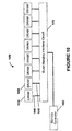
- Figure 10 illustrates a block diagram showing a burst-merging interface circuit connected to multiple DRAM devices with multiple independent data buses, in accordance with still yet another embodiment.
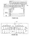
- Figures 18A and 18B illustrate a multi-rank buffer integrated circuit and DIMM, in accordance with still yet another embodiment.
- Figures 19A and 19B illustrate a buffer that provides a number of ranks on a D1MM equal to the number of valid integrated circuit selects from a host system, in accordance with another embodiment.
- the memory circuits 102 may include a monolithic memory circuit, a semiconductor die, a chip, a packaged memory circuit, or any other type of tangible memory circuit.
- the memory circuits 102 may tape the form of dynamic random access memory (DRAM) circuits.
- DRAM dynamic random access memory
- a plurality of memory circuits and a system are interfaced.
- the memory circuits and system may be interfaced utilizing an interface circuit.
- the interface circuit may include, for example, the interface circuit described above with, respect to Figure 1 .
- the interfacing may include facilitating communication between the memory circuits and the system.
- the memory circuits and system may be interfaced in any desired matter.
- the address may be translated in any desired manner. Such translation may include any converting, changing, transforming, etc. In one embodiment, the translation of the address may include shifting the address. In another embodiment, the address may be translated by mapping the address.
- the memory circuits may include physical memory circuits and the interface circuit may simulate a virtual memory circuit. To this end, the virtual memory circuit may optionally have a different (e.g. greater, etc.) number of row addresses associated therewith than the physical memory circuits.
- the translation may be performed as a function of the difference in the number of row addresses.
- the translation may translate the address to reflect the number of row addresses of the virtual memory circuit.
- the translation may optionally translate the address as a function of a column address and a row address.
- the interface circuit 470 may include emulation logic 480.
- the emulation logic 480 may be operable to receive and optionally store electrical signals (e.g. logic levels, commands, signals, protocol sequences, communications, etc.) from or through the system-facing interfaces, and may further be operable to process such electrical signals.
- the emulation logic 480 may respond to signals from system-facing interfaces by responding back to the system 420 and presenting signals to the system 420, and may also process the signals with other information previously stored.
- the emulation logic 480 may present signals to the physical memory circuits 410.
- the emulation logic 480 may perform any of the aforementioned functions in any order.
- the emulation logic 480 may be operable to adopt a personality, where such personality is capable of defining the physical memory circuit attributes.
- the personality may be effected via any combination of bonding options, strapping, programmable strapping, the wiring between the interface circuit 470 and the physical memory circuits 410.
- the personality may be effected via actual physical attributes (e.g. value of mode register, value of extended mode register) of the physical memory circuits 410 connected to the interface circuit 470 as determined when the interface circuit 470 and physical memory circuits 410 are powered up.
- commands from the memory controller that are directed to the DRAM devices may be issued with respect to command scheduling constraints (e.g. tRRD, tCCD, tFAW, tWTR, etc.).
- command scheduling constraints e.g. tRRD, tCCD, tFAW, tWTR, etc.
- the memory controller may expect that the logical device may take a relatively long period to perform a refresh command.
- the protocol translation and interface circuit 1210 may separately schedule refresh commands to each of the physical DRAM devices.
- the refresh of the larger logical DRAM device may take a relatively smaller period of time as compared with a refresh of a physical DRAM device of the same size.
- DDR3 memory systems may potentially require calibration sequences to ensure that the high speed data I/O circuits are periodically calibrated against thermal-variances induced timing drifts.
- the staggered refresh commands may also optionally guarantee I/O quiet time required to separately calibrate each of the independent physical DRAM devices.
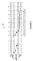
- FIG 14 illustrates a timing diagram 1400 showing the effect when a memory controller issues a column-access command early, in accordance with still yet another embodiment.
- the timing diagram 1400 may be associated with the architecture and environment of Figures 1-13 .
- the timing diagram 1400 may be associated with any desired environment. Further, the aforementioned definitions may equally apply to the description below.
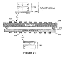
- a double rank registered DIMM that uses buffered DRAM stacks may have eighteen stacks, nine of which may be ion one side of the DIMM PCB and controlled by a first integrated circuit select signal from the host electronic system, and nine may be on the other side of the DIMM PCB and controlled by a second integrated circuit select signal from the host electronic system.
- Each of these stacks may contain a plurality of DRAM devices and a buffer integrated circuit.
- the buffer integrated circuit is now electrically between the host system and the stack on the DIMM PCB 2100 as well as the corresponding stack on the upgrade module PCB 2110.
- the buffer integrated circuit (2140), the DRAM stacks (2120), the DIMM PCB 2100, and the upgrade module PCB 2110 may be configured in various manners to achieve the same result, without deviating from the spirit or scope of the claims.
- the stack 2120 on the additional PCB may also contain a buffer integrated circuit. So, in this example, the upgrade module 2110 i may contain one or more buffer integrated circuits.
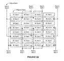
- Figure 22 illustrates an example of linear address mapping for use with a multi-rank buffer integrated circuit, in accordance with still yet another embodiment.
- the linear address mapping may be implemented in the context of Figures 1-21 .
- the linear address mapping may be implemented in any desired environment. Further, the aforementioned definitions may equally apply to the description below.
- Figure 25 illustrates an example of "bit slice” address mapping with a single rank buffer integrated circuit, in accordance with still yet another embodiment.
- the "bit slice” address mapping may be implemented in the context of Figures 1-24 .
- the "bit slice” address mapping may be implemented in any desired environment. Further, the aforementioned definitions may equally apply to the description below.
- Table 3 Host System Address (Virtual Bank) DRAM Device (Physical Device) Rank 0, Bank [0] M0 Rank 0, Bank [1] M1 Rank 0, Bank [2] M2 Rank 0, Bank [3] M3 Rank 0, Bank [4] M4 Rank 0, Bank [5] M5 Rank 0, Bank [6] M6 Rank 0, Bank [7] M7
- the stack of this example contains eight 512Mb DRAM devices so that the host system sees the stack as a single 4Gb device with eight banks.
- the address mappings shown above are for illustrative purposes only. Other mappings may be implemented without deviating from the spirit and scope of the claims.
- the DQ[0] signal may be driven later than the other data signals by the buffer integrated circuit (during a memory read) to compensate for the shorter trace length of the DQ[0] signal.
- the per-pin timing calibration and compensation circuits allow the buffer integrated circuit to delay the DQ[0] data signal such that all the data signals, DQ[7:0], are aligned for sampling during a memory write operation.
- the per-pin timing calibration and compensation circuits also allow the buffer integrated circuit to compensate for timing variations in the I/O pins of the DRAM devices.
- a specific pattern or sequence may be used by the buffer integrated circuit to perform the per-pin timing calibration of the signals that connect to the memory controller of the host system and the per-pin timing calibration of the signals that connect to the memory devices in the stack.
- the buffer integrated circuit may provide an interface to the host system that is narrower and faster than the interface to the DRAM integrated circuit.
- the buffer integrated circuit may have a 16- bit wide, 533MHz data rate interface to one or more DRAM devices but have an 8-bit wide, 1066MHz data rate interface to the host system.
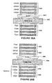
- DIMM PCB 2700 includes a buffered stack of DRAMs including decoupling layers.
- the buffered stack includes buffer 2710, a first set of DRAM devices 2720, a first decoupling layer 2730, a second set of DRAM devices 2740, and an optional second decoupling layer 2750.
- the stack also has an optional heat sink or spreader 2755.
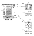
- FIG.27C illustrates top and side views of one embodiment of a decoupling layer.
- a decoupling layer 2775 includes one ore more decoupling capacitors 2770, signal/power/GND balls 2785, and one or more extra power/GND balls 2780.
- the extra power/GND balls 2780 increases thermal conductivity.
- the noise on the power and ground rails may be reduced by preventing the DRAM integrated circuits in the stack from performing an operation simultaneously.
- the buffer integrated circuit may be designed to stagger or spread out the refresh commands to the DRAM integrated circuits in the stack such that the peak current drawn from the power rails is reduced. For example, consider a stack with four 1Gb DDR2 SDRAM integrated circuits that are emulated by the buffer integrated circuit to appear as, a single 4Gb DDR2 SDRAM integrated circuit to the host system.
- the JEDEC specification provides for a refresh cycle time (i.e.
Landscapes
- Engineering & Computer Science (AREA)
- Theoretical Computer Science (AREA)
- Physics & Mathematics (AREA)
- General Engineering & Computer Science (AREA)
- General Physics & Mathematics (AREA)
- Dram (AREA)
- Memory System (AREA)
- Debugging And Monitoring (AREA)
- Stabilization Of Oscillater, Synchronisation, Frequency Synthesizers (AREA)
- Use Of Switch Circuits For Exchanges And Methods Of Control Of Multiplex Exchanges (AREA)
Applications Claiming Priority (7)
| Application Number | Priority Date | Filing Date | Title |
|---|---|---|---|
| US77241406P | 2006-02-09 | 2006-02-09 | |
| US11/461,437 US8077535B2 (en) | 2006-07-31 | 2006-07-31 | Memory refresh apparatus and method |
| US86562406P | 2006-11-13 | 2006-11-13 | |
| US11/702,960 US20080126690A1 (en) | 2006-02-09 | 2007-02-05 | Memory module with memory stack |
| US11/702,981 US8089795B2 (en) | 2006-02-09 | 2007-02-05 | Memory module with memory stack and interface with enhanced capabilities |
| EP11194862.6A EP2450800B1 (de) | 2006-02-09 | 2007-02-08 | Speicherschaltungssystem und -Verfahren |
| EP07750307A EP2005303B1 (de) | 2006-02-09 | 2007-02-08 | Speicherschaltungssystem und -verfahren |
Related Parent Applications (3)
| Application Number | Title | Priority Date | Filing Date |
|---|---|---|---|
| EP07750307A Division EP2005303B1 (de) | 2006-02-09 | 2007-02-08 | Speicherschaltungssystem und -verfahren |
| EP11194862.6A Division EP2450800B1 (de) | 2006-02-09 | 2007-02-08 | Speicherschaltungssystem und -Verfahren |
| EP11194862.6A Division-Into EP2450800B1 (de) | 2006-02-09 | 2007-02-08 | Speicherschaltungssystem und -Verfahren |
Publications (2)
| Publication Number | Publication Date |
|---|---|
| EP2696290A1 true EP2696290A1 (de) | 2014-02-12 |
| EP2696290B1 EP2696290B1 (de) | 2015-12-23 |
Family
ID=40028972
Family Applications (7)
| Application Number | Title | Priority Date | Filing Date |
|---|---|---|---|
| EP11194876.6A Active EP2450798B1 (de) | 2006-02-09 | 2007-02-08 | Speicherschaltungssystem und -Verfahren |
| EP11194862.6A Active EP2450800B1 (de) | 2006-02-09 | 2007-02-08 | Speicherschaltungssystem und -Verfahren |
| EP13191796.5A Ceased EP2706461A1 (de) | 2006-02-09 | 2007-02-08 | Speicherschaltungssystem und -Verfahren |
| EP07750307A Active EP2005303B1 (de) | 2006-02-09 | 2007-02-08 | Speicherschaltungssystem und -verfahren |
| EP13191794.0A Active EP2696290B1 (de) | 2006-02-09 | 2007-02-08 | Speicherschaltungssystem und -Verfahren |
| EP11194883.2A Active EP2458505B1 (de) | 2006-02-09 | 2007-02-08 | Speicherschaltungssystem und -Verfahren |
| EP17171824.0A Withdrawn EP3276495A1 (de) | 2006-02-09 | 2007-02-08 | Speicherschaltungssystem und -verfahren |
Family Applications Before (4)
| Application Number | Title | Priority Date | Filing Date |
|---|---|---|---|
| EP11194876.6A Active EP2450798B1 (de) | 2006-02-09 | 2007-02-08 | Speicherschaltungssystem und -Verfahren |
| EP11194862.6A Active EP2450800B1 (de) | 2006-02-09 | 2007-02-08 | Speicherschaltungssystem und -Verfahren |
| EP13191796.5A Ceased EP2706461A1 (de) | 2006-02-09 | 2007-02-08 | Speicherschaltungssystem und -Verfahren |
| EP07750307A Active EP2005303B1 (de) | 2006-02-09 | 2007-02-08 | Speicherschaltungssystem und -verfahren |
Family Applications After (2)
| Application Number | Title | Priority Date | Filing Date |
|---|---|---|---|
| EP11194883.2A Active EP2458505B1 (de) | 2006-02-09 | 2007-02-08 | Speicherschaltungssystem und -Verfahren |
| EP17171824.0A Withdrawn EP3276495A1 (de) | 2006-02-09 | 2007-02-08 | Speicherschaltungssystem und -verfahren |
Country Status (6)
| Country | Link |
|---|---|
| EP (7) | EP2450798B1 (de) |
| JP (3) | JP5205280B2 (de) |
| KR (3) | KR101404926B1 (de) |
| AT (1) | ATE554447T1 (de) |
| DK (3) | DK2005303T3 (de) |
| HK (1) | HK1250270A1 (de) |
Families Citing this family (32)
| Publication number | Priority date | Publication date | Assignee | Title |
|---|---|---|---|---|
| JP4861497B2 (ja) * | 2010-05-31 | 2012-01-25 | 株式会社東芝 | データ記憶装置及びメモリ調整方法 |
| US8582373B2 (en) * | 2010-08-31 | 2013-11-12 | Micron Technology, Inc. | Buffer die in stacks of memory dies and methods |
| JP2012099189A (ja) * | 2010-11-04 | 2012-05-24 | Elpida Memory Inc | 半導体装置 |
| JP5541373B2 (ja) | 2011-01-13 | 2014-07-09 | 富士通株式会社 | メモリコントローラ、及び情報処理装置 |
| JP2012146377A (ja) * | 2011-01-14 | 2012-08-02 | Elpida Memory Inc | 半導体装置 |
| JP5647014B2 (ja) * | 2011-01-17 | 2014-12-24 | ピーエスフォー ルクスコ エスエイアールエルPS4 Luxco S.a.r.l. | 半導体装置 |
| KR101937951B1 (ko) | 2012-05-31 | 2019-01-14 | 에스케이하이닉스 주식회사 | 반도체 집적회로 및 그의 구동방법 |
| US8811110B2 (en) | 2012-06-28 | 2014-08-19 | Intel Corporation | Configuration for power reduction in DRAM |
| US20150364466A1 (en) * | 2013-01-31 | 2015-12-17 | Hewlett-Packard Development Company, L.P. | Selecting circuits of a multi-level integrated circuit |
| KR101821633B1 (ko) | 2013-03-14 | 2018-03-08 | 삼성전자주식회사 | 메모리 시스템 |
| US9679615B2 (en) * | 2013-03-15 | 2017-06-13 | Micron Technology, Inc. | Flexible memory system with a controller and a stack of memory |
| US9658783B2 (en) * | 2013-03-27 | 2017-05-23 | Hitachi, Ltd. | DRAM having SDRAM interface and flash memory consolidated memory module |
| CN105027092B (zh) * | 2013-03-27 | 2018-01-30 | 株式会社日立制作所 | 具有sdram接口的dram、混合闪存存储器模块 |
| WO2014203383A1 (ja) * | 2013-06-20 | 2014-12-24 | 株式会社日立製作所 | 異種メモリを混載したメモリモジュール、及びそれを搭載した情報処理装置 |
| US9921980B2 (en) | 2013-08-12 | 2018-03-20 | Micron Technology, Inc. | Apparatuses and methods for configuring I/Os of memory for hybrid memory modules |
| US9805775B1 (en) | 2013-11-08 | 2017-10-31 | Altera Corporation | Integrated circuits with improved memory controllers |
| US9760138B2 (en) * | 2014-04-25 | 2017-09-12 | Microsoft Technology Licensing, Llc | Load scheduling in multi-battery devices |
| JP5775629B2 (ja) * | 2014-07-29 | 2015-09-09 | ルネサスエレクトロニクス株式会社 | 半導体集積回路 |
| US10261697B2 (en) | 2015-06-08 | 2019-04-16 | Samsung Electronics Co., Ltd. | Storage device and operating method of storage device |
| KR102274038B1 (ko) * | 2015-08-03 | 2021-07-09 | 삼성전자주식회사 | 백업 기능을 갖는 메모리 모듈 |
| US10592114B2 (en) | 2016-03-03 | 2020-03-17 | Samsung Electronics Co., Ltd. | Coordinated in-module RAS features for synchronous DDR compatible memory |
| US9830086B2 (en) * | 2016-03-03 | 2017-11-28 | Samsung Electronics Co., Ltd. | Hybrid memory controller for arbitrating access to volatile and non-volatile memories in a hybrid memory group |
| US10810144B2 (en) * | 2016-06-08 | 2020-10-20 | Samsung Electronics Co., Ltd. | System and method for operating a DRR-compatible asynchronous memory module |
| KR102716191B1 (ko) * | 2016-12-06 | 2024-10-11 | 삼성전자주식회사 | 반도체 메모리 장치 및 이를 구비하는 메모리 모듈 |
| WO2018216081A1 (ja) * | 2017-05-22 | 2018-11-29 | ゼンテルジャパン株式会社 | 半導体記憶システム |
| KR20210031266A (ko) * | 2019-09-11 | 2021-03-19 | 삼성전자주식회사 | 인터페이스 회로, 메모리 장치, 저장 장치 및 메모리 장치의 동작 방법 |
| WO2021199447A1 (ja) * | 2020-04-03 | 2021-10-07 | ウルトラメモリ株式会社 | メモリユニット、半導体モジュール、dimmモジュール、及びそれらの製造方法 |
| US11222702B1 (en) | 2020-07-09 | 2022-01-11 | Micron Technology, Inc. | Noise reduction during parallel plane access in a multi-plane memory device |
| US11494120B2 (en) | 2020-10-02 | 2022-11-08 | Qualcomm Incorporated | Adaptive memory transaction scheduling |
| JP7883885B2 (ja) * | 2022-06-03 | 2026-07-02 | 株式会社半導体エネルギー研究所 | 半導体装置 |
| KR20260063078A (ko) | 2024-10-30 | 2026-05-07 | 연세대학교 산학협력단 | 스큐 저항 pid 장치 및 처리 방법 |
| CN120371227A (zh) * | 2025-06-27 | 2025-07-25 | 西安紫光国芯半导体股份有限公司 | 一种存储模组、存储系统及电子系统 |
Citations (5)
| Publication number | Priority date | Publication date | Assignee | Title |
|---|---|---|---|---|
| EP0132129A2 (de) * | 1983-07-14 | 1985-01-23 | BURROUGHS CORPORATION (a Michigan corporation) | Adressumsetzungspuffer |
| US5765203A (en) * | 1995-12-19 | 1998-06-09 | Seagate Technology, Inc. | Storage and addressing method for a buffer memory control system for accessing user and error imformation |
| US5960468A (en) * | 1997-04-30 | 1999-09-28 | Sony Corporation | Asynchronous memory interface for a video processor with a 2N sized buffer and N+1 bit wide gray coded counters |
| US6044028A (en) * | 1995-10-16 | 2000-03-28 | Seiko Epson Corporation | Semiconductor storage device and electronic equipment using the same |
| WO2000045270A2 (en) * | 1999-01-28 | 2000-08-03 | Infineon Technologies Ag | Techniques for improving memory access in a virtual memory system |
Family Cites Families (34)
| Publication number | Priority date | Publication date | Assignee | Title |
|---|---|---|---|---|
| US5369749A (en) * | 1989-05-17 | 1994-11-29 | Ibm Corporation | Method and apparatus for the direct transfer of information between application programs running on distinct processors without utilizing the services of one or both operating systems |
| JP3078136B2 (ja) * | 1992-11-27 | 2000-08-21 | 沖電気工業株式会社 | 画像メモリ装置 |
| WO1995005676A1 (en) * | 1993-08-13 | 1995-02-23 | Irvine Sensors Corporation | Stack of ic chips as substitute for single ic chip |
| JPH08278916A (ja) * | 1994-11-30 | 1996-10-22 | Hitachi Ltd | マルチチャネルメモリシステム、転送情報同期化方法及び信号転送回路 |
| KR0164358B1 (ko) * | 1995-08-31 | 1999-02-18 | 김광호 | 반도체 메모리 장치의 서브워드라인 디코더 |
| US5761694A (en) * | 1995-11-30 | 1998-06-02 | Cirrus Logic, Inc. | Multi-bank memory system and method having addresses switched between the row and column decoders in different banks |
| US5926827A (en) * | 1996-02-09 | 1999-07-20 | International Business Machines Corp. | High density SIMM or DIMM with RAS address re-mapping |
| JPH10233091A (ja) * | 1997-02-21 | 1998-09-02 | Hitachi Ltd | 半導体記憶装置およびデータ処理装置 |
| JPH10260895A (ja) * | 1997-03-19 | 1998-09-29 | Hitachi Ltd | 半導体記憶装置およびそれを用いた計算機システム |
| US6067255A (en) * | 1997-07-03 | 2000-05-23 | Samsung Electronics Co., Ltd. | Merged memory and logic (MML) integrated circuits including independent memory bank signals and methods |
| US6351427B1 (en) * | 1997-12-10 | 2002-02-26 | Texas Instruments Incorporated | Stored write scheme for high speed/wide bandwidth memory devices |
| JP3922487B2 (ja) * | 1998-02-04 | 2007-05-30 | 松下電器産業株式会社 | メモリ制御装置および方法 |
| US6226730B1 (en) * | 1998-06-05 | 2001-05-01 | Intel Corporation | Achieving page hit memory cycles on a virtual address reference |
| JP4540137B2 (ja) * | 1998-07-24 | 2010-09-08 | ルネサスエレクトロニクス株式会社 | 同期型半導体記憶装置 |
| US6526484B1 (en) * | 1998-11-16 | 2003-02-25 | Infineon Technologies Ag | Methods and apparatus for reordering of the memory requests to achieve higher average utilization of the command and data bus |
| KR100304705B1 (ko) * | 1999-03-03 | 2001-10-29 | 윤종용 | 포스티드 카스 레이턴시 기능을 가지는 동기식 반도체 메모리 장치 및 카스 레이턴시 제어 방법 |
| US6389514B1 (en) * | 1999-03-25 | 2002-05-14 | Hewlett-Packard Company | Method and computer system for speculatively closing pages in memory |
| US6683372B1 (en) * | 1999-11-18 | 2004-01-27 | Sun Microsystems, Inc. | Memory expansion module with stacked memory packages and a serial storage unit |
| KR100344217B1 (ko) * | 2000-07-04 | 2002-07-20 | 주식회사 케이이씨메카트로닉스 | 듀얼포트 메모리를 이용한 통신 인터페이스회로 |
| US6487102B1 (en) * | 2000-09-18 | 2002-11-26 | Intel Corporation | Memory module having buffer for isolating stacked memory devices |
| JP2002288037A (ja) * | 2001-03-27 | 2002-10-04 | Sony Corp | メモリ制御装置及び方法 |
| US6915402B2 (en) * | 2001-05-23 | 2005-07-05 | Hewlett-Packard Development Company, L.P. | Method and system for creating secure address space using hardware memory router |
| JP3799251B2 (ja) * | 2001-08-24 | 2006-07-19 | エルピーダメモリ株式会社 | メモリデバイス及びメモリシステム |
| CN1280734C (zh) * | 2001-09-07 | 2006-10-18 | 皇家菲利浦电子有限公司 | 用于分段存取控制的控制装置和方法和具有该控制装置的视频存储器装置 |
| US6914324B2 (en) * | 2001-10-26 | 2005-07-05 | Staktek Group L.P. | Memory expansion and chip scale stacking system and method |
| US6950910B2 (en) * | 2001-11-08 | 2005-09-27 | Freescale Semiconductor, Inc. | Mobile wireless communication device architectures and methods therefor |
| US7480911B2 (en) * | 2002-05-09 | 2009-01-20 | International Business Machines Corporation | Method and apparatus for dynamically allocating and deallocating processors in a logical partitioned data processing system |
| JP2006509315A (ja) * | 2002-12-04 | 2006-03-16 | コーニンクレッカ フィリップス エレクトロニクス エヌ ヴィ | 携帯可能なコンテンツ提示装置、及びこれらのためのコンテンツを提示する方法 |
| JP4419049B2 (ja) * | 2003-04-21 | 2010-02-24 | エルピーダメモリ株式会社 | メモリモジュール及びメモリシステム |
| JP4346369B2 (ja) * | 2003-08-08 | 2009-10-21 | 株式会社メルコホールディングス | メモリモジュールおよびメモリ用補助モジュール |
| JP3896112B2 (ja) * | 2003-12-25 | 2007-03-22 | エルピーダメモリ株式会社 | 半導体集積回路装置 |
| KR100604843B1 (ko) * | 2004-03-26 | 2006-07-31 | 삼성전자주식회사 | 온-다이 종단 회로를 구비한 메모리 모듈 및 그 제어 방법 |
| TWI299497B (en) * | 2004-06-24 | 2008-08-01 | Via Tech Inc | Method and related apparatus for accessing memory apparatus |
| JP4534132B2 (ja) * | 2004-06-29 | 2010-09-01 | エルピーダメモリ株式会社 | 積層型半導体メモリ装置 |
-
2007
- 2007-02-08 EP EP11194876.6A patent/EP2450798B1/de active Active
- 2007-02-08 EP EP11194862.6A patent/EP2450800B1/de active Active
- 2007-02-08 EP EP13191796.5A patent/EP2706461A1/de not_active Ceased
- 2007-02-08 EP EP07750307A patent/EP2005303B1/de active Active
- 2007-02-08 DK DK07750307.6T patent/DK2005303T3/da active
- 2007-02-08 JP JP2008554369A patent/JP5205280B2/ja not_active Expired - Fee Related
- 2007-02-08 KR KR1020147007335A patent/KR101404926B1/ko not_active Expired - Fee Related
- 2007-02-08 AT AT07750307T patent/ATE554447T1/de active
- 2007-02-08 KR KR1020087019582A patent/KR101343252B1/ko active Active
- 2007-02-08 EP EP13191794.0A patent/EP2696290B1/de active Active
- 2007-02-08 DK DK11194883.2T patent/DK2458505T3/en active
- 2007-02-08 KR KR1020137029741A patent/KR101429869B1/ko active Active
- 2007-02-08 EP EP11194883.2A patent/EP2458505B1/de active Active
- 2007-02-08 EP EP17171824.0A patent/EP3276495A1/de not_active Withdrawn
- 2007-02-08 DK DK13191794.0T patent/DK2696290T3/en active
-
2012
- 2012-09-07 JP JP2012197678A patent/JP5730252B2/ja not_active Expired - Fee Related
- 2012-09-07 JP JP2012197675A patent/JP5730251B2/ja not_active Expired - Fee Related
-
2018
- 2018-07-26 HK HK18109715.5A patent/HK1250270A1/en unknown
Patent Citations (5)
| Publication number | Priority date | Publication date | Assignee | Title |
|---|---|---|---|---|
| EP0132129A2 (de) * | 1983-07-14 | 1985-01-23 | BURROUGHS CORPORATION (a Michigan corporation) | Adressumsetzungspuffer |
| US6044028A (en) * | 1995-10-16 | 2000-03-28 | Seiko Epson Corporation | Semiconductor storage device and electronic equipment using the same |
| US5765203A (en) * | 1995-12-19 | 1998-06-09 | Seagate Technology, Inc. | Storage and addressing method for a buffer memory control system for accessing user and error imformation |
| US5960468A (en) * | 1997-04-30 | 1999-09-28 | Sony Corporation | Asynchronous memory interface for a video processor with a 2N sized buffer and N+1 bit wide gray coded counters |
| WO2000045270A2 (en) * | 1999-01-28 | 2000-08-03 | Infineon Technologies Ag | Techniques for improving memory access in a virtual memory system |
Also Published As
| Publication number | Publication date |
|---|---|
| KR101404926B1 (ko) | 2014-06-10 |
| ATE554447T1 (de) | 2012-05-15 |
| DK2458505T3 (en) | 2014-12-01 |
| JP2009526323A (ja) | 2009-07-16 |
| KR20130141693A (ko) | 2013-12-26 |
| DK2005303T3 (da) | 2012-07-23 |
| EP2005303A4 (de) | 2009-09-16 |
| JP5730251B2 (ja) | 2015-06-03 |
| EP2450798B1 (de) | 2013-10-30 |
| EP2696290B1 (de) | 2015-12-23 |
| EP2458505B1 (de) | 2014-10-08 |
| JP5730252B2 (ja) | 2015-06-03 |
| KR20080108975A (ko) | 2008-12-16 |
| EP3276495A1 (de) | 2018-01-31 |
| EP2450800A1 (de) | 2012-05-09 |
| JP2013012232A (ja) | 2013-01-17 |
| EP2005303A2 (de) | 2008-12-24 |
| EP2706461A1 (de) | 2014-03-12 |
| JP2013012233A (ja) | 2013-01-17 |
| EP2458505A1 (de) | 2012-05-30 |
| EP2450798A1 (de) | 2012-05-09 |
| KR101429869B1 (ko) | 2014-08-12 |
| HK1250270A1 (en) | 2018-12-07 |
| EP2450800B1 (de) | 2014-04-23 |
| EP2005303B1 (de) | 2012-04-18 |
| DK2696290T3 (en) | 2016-02-15 |
| KR20140056349A (ko) | 2014-05-09 |
| JP5205280B2 (ja) | 2013-06-05 |
| KR101343252B1 (ko) | 2013-12-18 |
Similar Documents
| Publication | Publication Date | Title |
|---|---|---|
| EP2450800B1 (de) | Speicherschaltungssystem und -Verfahren | |
| US8089795B2 (en) | Memory module with memory stack and interface with enhanced capabilities | |
| WO2007095080A2 (en) | Memory circuit system and method | |
| US20080126690A1 (en) | Memory module with memory stack | |
| US9171585B2 (en) | Configurable memory circuit system and method | |
| US9632929B2 (en) | Translating an address associated with a command communicated between a system and memory circuits | |
| US9542353B2 (en) | System and method for reducing command scheduling constraints of memory circuits | |
| US8400807B2 (en) | Semiconductor system | |
| US8917571B2 (en) | Configurable-width memory channels for stacked memory structures | |
| US8881389B2 (en) | Methods of flash dual inline memory modules with flash memory | |
| WO2024054755A2 (en) | Dynamic memory operations |
Legal Events
| Date | Code | Title | Description |
|---|---|---|---|
| AC | Divisional application: reference to earlier application |
Ref document number: 2005303 Country of ref document: EP Kind code of ref document: P Ref document number: 2450800 Country of ref document: EP Kind code of ref document: P |
|
| AK | Designated contracting states |
Kind code of ref document: A1 Designated state(s): AT BE BG CH CY CZ DE DK EE ES FI FR GB GR HU IE IS IT LI LT LU LV MC NL PL PT RO SE SI SK TR |
|
| PUAI | Public reference made under article 153(3) epc to a published international application that has entered the european phase |
Free format text: ORIGINAL CODE: 0009012 |
|
| 17P | Request for examination filed |
Effective date: 20140716 |
|
| RBV | Designated contracting states (corrected) |
Designated state(s): AT BE BG CH CY CZ DE DK EE ES FI FR GB GR HU IE IS IT LI LT LU LV MC NL PL PT RO SE SI SK TR |
|
| RIN1 | Information on inventor provided before grant (corrected) |
Inventor name: SCHAKEL, KEITH R. Inventor name: WEBER, FREDERICK DANIEL Inventor name: RAJAN, SURESH NATARAJAN Inventor name: WANG, DAVID T. Inventor name: SMITH, MICHAEL JOHN SEBASTIAN |
|
| GRAP | Despatch of communication of intention to grant a patent |
Free format text: ORIGINAL CODE: EPIDOSNIGR1 |
|
| RIC1 | Information provided on ipc code assigned before grant |
Ipc: G06F 13/16 20060101ALI20150528BHEP Ipc: G06F 12/10 20060101AFI20150528BHEP |
|
| INTG | Intention to grant announced |
Effective date: 20150618 |
|
| GRAS | Grant fee paid |
Free format text: ORIGINAL CODE: EPIDOSNIGR3 |
|
| GRAA | (expected) grant |
Free format text: ORIGINAL CODE: 0009210 |
|
| AC | Divisional application: reference to earlier application |
Ref document number: 2005303 Country of ref document: EP Kind code of ref document: P Ref document number: 2450800 Country of ref document: EP Kind code of ref document: P |
|
| AK | Designated contracting states |
Kind code of ref document: B1 Designated state(s): AT BE BG CH CY CZ DE DK EE ES FI FR GB GR HU IE IS IT LI LT LU LV MC NL PL PT RO SE SI SK TR |
|
| REG | Reference to a national code |
Ref country code: GB Ref legal event code: FG4D |
|
| REG | Reference to a national code |
Ref country code: CH Ref legal event code: EP |
|
| REG | Reference to a national code |
Ref country code: IE Ref legal event code: FG4D |
|
| REG | Reference to a national code |
Ref country code: AT Ref legal event code: REF Ref document number: 766817 Country of ref document: AT Kind code of ref document: T Effective date: 20160115 |
|
| REG | Reference to a national code |
Ref country code: CH Ref legal event code: NV Representative=s name: KIRKER AND CIE S.A., CH |
|
| REG | Reference to a national code |
Ref country code: DK Ref legal event code: T3 Effective date: 20160211 |
|
| REG | Reference to a national code |
Ref country code: FR Ref legal event code: PLFP Year of fee payment: 10 |
|
| REG | Reference to a national code |
Ref country code: DE Ref legal event code: R096 Ref document number: 602007044340 Country of ref document: DE |
|
| REG | Reference to a national code |
Ref country code: SE Ref legal event code: TRGR |
|
| REG | Reference to a national code |
Ref country code: NL Ref legal event code: FP |
|
| REG | Reference to a national code |
Ref country code: LT Ref legal event code: MG4D |
|
| PG25 | Lapsed in a contracting state [announced via postgrant information from national office to epo] |
Ref country code: LT Free format text: LAPSE BECAUSE OF FAILURE TO SUBMIT A TRANSLATION OF THE DESCRIPTION OR TO PAY THE FEE WITHIN THE PRESCRIBED TIME-LIMIT Effective date: 20151223 |
|
| REG | Reference to a national code |
Ref country code: AT Ref legal event code: MK05 Ref document number: 766817 Country of ref document: AT Kind code of ref document: T Effective date: 20151223 |
|
| PG25 | Lapsed in a contracting state [announced via postgrant information from national office to epo] |
Ref country code: LV Free format text: LAPSE BECAUSE OF FAILURE TO SUBMIT A TRANSLATION OF THE DESCRIPTION OR TO PAY THE FEE WITHIN THE PRESCRIBED TIME-LIMIT Effective date: 20151223 Ref country code: GR Free format text: LAPSE BECAUSE OF FAILURE TO SUBMIT A TRANSLATION OF THE DESCRIPTION OR TO PAY THE FEE WITHIN THE PRESCRIBED TIME-LIMIT Effective date: 20160324 |
|
| PG25 | Lapsed in a contracting state [announced via postgrant information from national office to epo] |
Ref country code: IT Free format text: LAPSE BECAUSE OF FAILURE TO SUBMIT A TRANSLATION OF THE DESCRIPTION OR TO PAY THE FEE WITHIN THE PRESCRIBED TIME-LIMIT Effective date: 20151223 Ref country code: CZ Free format text: LAPSE BECAUSE OF FAILURE TO SUBMIT A TRANSLATION OF THE DESCRIPTION OR TO PAY THE FEE WITHIN THE PRESCRIBED TIME-LIMIT Effective date: 20151223 Ref country code: ES Free format text: LAPSE BECAUSE OF FAILURE TO SUBMIT A TRANSLATION OF THE DESCRIPTION OR TO PAY THE FEE WITHIN THE PRESCRIBED TIME-LIMIT Effective date: 20151223 |
|
| PG25 | Lapsed in a contracting state [announced via postgrant information from national office to epo] |
Ref country code: IS Free format text: LAPSE BECAUSE OF FAILURE TO SUBMIT A TRANSLATION OF THE DESCRIPTION OR TO PAY THE FEE WITHIN THE PRESCRIBED TIME-LIMIT Effective date: 20160423 Ref country code: SK Free format text: LAPSE BECAUSE OF FAILURE TO SUBMIT A TRANSLATION OF THE DESCRIPTION OR TO PAY THE FEE WITHIN THE PRESCRIBED TIME-LIMIT Effective date: 20151223 Ref country code: PT Free format text: LAPSE BECAUSE OF FAILURE TO SUBMIT A TRANSLATION OF THE DESCRIPTION OR TO PAY THE FEE WITHIN THE PRESCRIBED TIME-LIMIT Effective date: 20160426 Ref country code: AT Free format text: LAPSE BECAUSE OF FAILURE TO SUBMIT A TRANSLATION OF THE DESCRIPTION OR TO PAY THE FEE WITHIN THE PRESCRIBED TIME-LIMIT Effective date: 20151223 Ref country code: EE Free format text: LAPSE BECAUSE OF FAILURE TO SUBMIT A TRANSLATION OF THE DESCRIPTION OR TO PAY THE FEE WITHIN THE PRESCRIBED TIME-LIMIT Effective date: 20151223 Ref country code: PL Free format text: LAPSE BECAUSE OF FAILURE TO SUBMIT A TRANSLATION OF THE DESCRIPTION OR TO PAY THE FEE WITHIN THE PRESCRIBED TIME-LIMIT Effective date: 20151223 Ref country code: RO Free format text: LAPSE BECAUSE OF FAILURE TO SUBMIT A TRANSLATION OF THE DESCRIPTION OR TO PAY THE FEE WITHIN THE PRESCRIBED TIME-LIMIT Effective date: 20151223 |
|
| REG | Reference to a national code |
Ref country code: DE Ref legal event code: R097 Ref document number: 602007044340 Country of ref document: DE |
|
| PG25 | Lapsed in a contracting state [announced via postgrant information from national office to epo] |
Ref country code: MC Free format text: LAPSE BECAUSE OF FAILURE TO SUBMIT A TRANSLATION OF THE DESCRIPTION OR TO PAY THE FEE WITHIN THE PRESCRIBED TIME-LIMIT Effective date: 20151223 Ref country code: LU Free format text: LAPSE BECAUSE OF FAILURE TO SUBMIT A TRANSLATION OF THE DESCRIPTION OR TO PAY THE FEE WITHIN THE PRESCRIBED TIME-LIMIT Effective date: 20160208 |
|
| PLBE | No opposition filed within time limit |
Free format text: ORIGINAL CODE: 0009261 |
|
| STAA | Information on the status of an ep patent application or granted ep patent |
Free format text: STATUS: NO OPPOSITION FILED WITHIN TIME LIMIT |
|
| 26N | No opposition filed |
Effective date: 20160926 |
|
| REG | Reference to a national code |
Ref country code: FR Ref legal event code: PLFP Year of fee payment: 11 |
|
| PG25 | Lapsed in a contracting state [announced via postgrant information from national office to epo] |
Ref country code: SI Free format text: LAPSE BECAUSE OF FAILURE TO SUBMIT A TRANSLATION OF THE DESCRIPTION OR TO PAY THE FEE WITHIN THE PRESCRIBED TIME-LIMIT Effective date: 20151223 |
|
| REG | Reference to a national code |
Ref country code: DE Ref legal event code: R082 Ref document number: 602007044340 Country of ref document: DE Representative=s name: WUESTHOFF & WUESTHOFF, PATENTANWAELTE PARTG MB, DE Ref country code: DE Ref legal event code: R081 Ref document number: 602007044340 Country of ref document: DE Owner name: GOOGLE LLC (N.D.GES.D. STAATES DELAWARE), MOUN, US Free format text: FORMER OWNER: GOOGLE, INC., MOUNTAIN VIEW, CALIF., US |
|
| REG | Reference to a national code |
Ref country code: FR Ref legal event code: PLFP Year of fee payment: 12 |
|
| REG | Reference to a national code |
Ref country code: FR Ref legal event code: CD Owner name: GOOGLE INC., US Effective date: 20180213 Ref country code: FR Ref legal event code: CJ Effective date: 20180213 |
|
| PGFP | Annual fee paid to national office [announced via postgrant information from national office to epo] |
Ref country code: NL Payment date: 20180226 Year of fee payment: 12 |
|
| PGFP | Annual fee paid to national office [announced via postgrant information from national office to epo] |
Ref country code: DK Payment date: 20180223 Year of fee payment: 12 Ref country code: DE Payment date: 20180227 Year of fee payment: 12 Ref country code: GB Payment date: 20180227 Year of fee payment: 12 Ref country code: FI Payment date: 20180227 Year of fee payment: 12 Ref country code: CH Payment date: 20180227 Year of fee payment: 12 |
|
| PG25 | Lapsed in a contracting state [announced via postgrant information from national office to epo] |
Ref country code: HU Free format text: LAPSE BECAUSE OF FAILURE TO SUBMIT A TRANSLATION OF THE DESCRIPTION OR TO PAY THE FEE WITHIN THE PRESCRIBED TIME-LIMIT; INVALID AB INITIO Effective date: 20070208 Ref country code: CY Free format text: LAPSE BECAUSE OF FAILURE TO SUBMIT A TRANSLATION OF THE DESCRIPTION OR TO PAY THE FEE WITHIN THE PRESCRIBED TIME-LIMIT Effective date: 20151223 |
|
| PGFP | Annual fee paid to national office [announced via postgrant information from national office to epo] |
Ref country code: FR Payment date: 20180227 Year of fee payment: 12 Ref country code: SE Payment date: 20180227 Year of fee payment: 12 |
|
| PG25 | Lapsed in a contracting state [announced via postgrant information from national office to epo] |
Ref country code: TR Free format text: LAPSE BECAUSE OF FAILURE TO SUBMIT A TRANSLATION OF THE DESCRIPTION OR TO PAY THE FEE WITHIN THE PRESCRIBED TIME-LIMIT Effective date: 20151223 |
|
| PG25 | Lapsed in a contracting state [announced via postgrant information from national office to epo] |
Ref country code: BG Free format text: LAPSE BECAUSE OF FAILURE TO SUBMIT A TRANSLATION OF THE DESCRIPTION OR TO PAY THE FEE WITHIN THE PRESCRIBED TIME-LIMIT Effective date: 20151223 |
|
| REG | Reference to a national code |
Ref country code: DE Ref legal event code: R119 Ref document number: 602007044340 Country of ref document: DE |
|
| REG | Reference to a national code |
Ref country code: DK Ref legal event code: EBP Effective date: 20190228 |
|
| REG | Reference to a national code |
Ref country code: CH Ref legal event code: PL |
|
| REG | Reference to a national code |
Ref country code: SE Ref legal event code: EUG |
|
| REG | Reference to a national code |
Ref country code: NL Ref legal event code: MM Effective date: 20190301 |
|
| GBPC | Gb: european patent ceased through non-payment of renewal fee |
Effective date: 20190208 |
|
| PG25 | Lapsed in a contracting state [announced via postgrant information from national office to epo] |
Ref country code: SE Free format text: LAPSE BECAUSE OF NON-PAYMENT OF DUE FEES Effective date: 20190209 Ref country code: FI Free format text: LAPSE BECAUSE OF NON-PAYMENT OF DUE FEES Effective date: 20190208 |
|
| PG25 | Lapsed in a contracting state [announced via postgrant information from national office to epo] |
Ref country code: CH Free format text: LAPSE BECAUSE OF NON-PAYMENT OF DUE FEES Effective date: 20190228 Ref country code: LI Free format text: LAPSE BECAUSE OF NON-PAYMENT OF DUE FEES Effective date: 20190228 |
|
| PG25 | Lapsed in a contracting state [announced via postgrant information from national office to epo] |
Ref country code: NL Free format text: LAPSE BECAUSE OF NON-PAYMENT OF DUE FEES Effective date: 20190301 Ref country code: DK Free format text: LAPSE BECAUSE OF NON-PAYMENT OF DUE FEES Effective date: 20190228 Ref country code: DE Free format text: LAPSE BECAUSE OF NON-PAYMENT OF DUE FEES Effective date: 20190903 Ref country code: GB Free format text: LAPSE BECAUSE OF NON-PAYMENT OF DUE FEES Effective date: 20190208 |
|
| PG25 | Lapsed in a contracting state [announced via postgrant information from national office to epo] |
Ref country code: FR Free format text: LAPSE BECAUSE OF NON-PAYMENT OF DUE FEES Effective date: 20190228 |
|
| P01 | Opt-out of the competence of the unified patent court (upc) registered |
Effective date: 20230505 |
|
| PGFP | Annual fee paid to national office [announced via postgrant information from national office to epo] |
Ref country code: IE Payment date: 20260227 Year of fee payment: 20 |
|
| PGFP | Annual fee paid to national office [announced via postgrant information from national office to epo] |
Ref country code: BE Payment date: 20260227 Year of fee payment: 20 |