EP2743659B1 - Verfahren zur Umsetzung einer Infraroterfassungsvorrichtung - Google Patents
Verfahren zur Umsetzung einer Infraroterfassungsvorrichtung Download PDFInfo
- Publication number
- EP2743659B1 EP2743659B1 EP13197327.3A EP13197327A EP2743659B1 EP 2743659 B1 EP2743659 B1 EP 2743659B1 EP 13197327 A EP13197327 A EP 13197327A EP 2743659 B1 EP2743659 B1 EP 2743659B1
- Authority
- EP
- European Patent Office
- Prior art keywords
- infrared thermal
- thermal detector
- layer
- infrared
- electrically
- Prior art date
- Legal status (The legal status is an assumption and is not a legal conclusion. Google has not performed a legal analysis and makes no representation as to the accuracy of the status listed.)
- Active
Links
Images







Classifications
-
- G—PHYSICS
- G01—MEASURING; TESTING
- G01J—MEASUREMENT OF INTENSITY, VELOCITY, SPECTRAL CONTENT, POLARISATION, PHASE OR PULSE CHARACTERISTICS OF INFRARED, VISIBLE OR ULTRAVIOLET LIGHT; COLORIMETRY; RADIATION PYROMETRY
- G01J5/00—Radiation pyrometry, e.g. infrared or optical thermometry
- G01J5/10—Radiation pyrometry, e.g. infrared or optical thermometry using electric radiation detectors
- G01J5/20—Radiation pyrometry, e.g. infrared or optical thermometry using electric radiation detectors using resistors, thermistors or semiconductors sensitive to radiation, e.g. photoconductive devices
-
- G—PHYSICS
- G01—MEASURING; TESTING
- G01J—MEASUREMENT OF INTENSITY, VELOCITY, SPECTRAL CONTENT, POLARISATION, PHASE OR PULSE CHARACTERISTICS OF INFRARED, VISIBLE OR ULTRAVIOLET LIGHT; COLORIMETRY; RADIATION PYROMETRY
- G01J5/00—Radiation pyrometry, e.g. infrared or optical thermometry
- G01J5/02—Constructional details
- G01J5/0225—Shape of the cavity itself or of elements contained in or suspended over the cavity
- G01J5/024—Special manufacturing steps or sacrificial layers or layer structures
-
- H—ELECTRICITY
- H10—SEMICONDUCTOR DEVICES; ELECTRIC SOLID-STATE DEVICES NOT OTHERWISE PROVIDED FOR
- H10F—INORGANIC SEMICONDUCTOR DEVICES SENSITIVE TO INFRARED RADIATION, LIGHT, ELECTROMAGNETIC RADIATION OF SHORTER WAVELENGTH OR CORPUSCULAR RADIATION
- H10F71/00—Manufacture or treatment of devices covered by this subclass
-
- G—PHYSICS
- G01—MEASURING; TESTING
- G01J—MEASUREMENT OF INTENSITY, VELOCITY, SPECTRAL CONTENT, POLARISATION, PHASE OR PULSE CHARACTERISTICS OF INFRARED, VISIBLE OR ULTRAVIOLET LIGHT; COLORIMETRY; RADIATION PYROMETRY
- G01J5/00—Radiation pyrometry, e.g. infrared or optical thermometry
- G01J5/10—Radiation pyrometry, e.g. infrared or optical thermometry using electric radiation detectors
- G01J2005/106—Arrays
Definitions
- the present invention relates to a method for producing an infrared detection device, comprising at least one thermal detector of infrared radiation capable of operating at room temperature, for example of the micro-bolometer type, as well as such an infrared detection device.
- the detection device obtained by the method according to the invention can in particular be used in the fields of infrared imaging, thermography, management of automation for example in buildings, or even gas detection via a measurement of absorption in an infrared spectrum capable of being detected by the infrared thermal detector.
- An infrared detection device generally comprises a plurality of unit detectors of infrared radiation, each forming a pixel of the detection device, connected to an electronic reading circuit responsible for operating and exploiting the signals delivered by the pixels.
- Each of these infrared thermal detectors, or pixels comprises an absorbent membrane suspended by thermally insulating support means above a semiconductor substrate (for example silicon) comprising the electronic reading circuit used for processing the signals delivered by infrared thermal detectors.
- Infrared thermal detectors can be produced by collective microelectronic processes, that is to say all produced simultaneously, for the entire wafer, or substrate or wafer, of semiconductor. These collective processes allow the production of matrices of infrared thermal detectors of great complexity, comprising a large number of pixels (for example in the form of matrices of 640 ⁇ 480 pixels), and also the production of a large number of matrices per wafer .
- Microelectronics techniques also make it possible to integrate, on the wafer, electronic reading circuits of the VLSI type (“Very Large Scale Integration", or very large scale integration) able to read a matrix of pixels.
- the electronic reading circuit is generally integrated in CMOS technology and in this case comprises deep semiconductor-based layers where electronic devices including transistors and diodes are installed (“Front End” part of the electronic reading circuit) and surface layers where several levels of electrical interconnections are provided (“Back End” part of the electronic reading circuit) to connect the electronic devices together.
- Adequate processing of the signals delivered by a large number of pixels can be obtained by making at least as many electrical links as pixels between these pixels and the reading circuit. These electrical links are therefore also produced collectively, according to different technical options which depend on the architecture chosen to produce the infrared detection device, namely the matrix of infrared thermal detectors coupled to its reading circuit.
- the matrix of infrared thermal detectors is manufactured above the reading circuit previously produced on a silicon substrate.
- the detector matrix is produced using a technique called surface micro-machining which consists of constructing the infrared thermal detectors on the surface of a sacrificial layer placed between the surface of the reading circuit and the underside of the detectors. Electrical links are made through the thickness of the sacrificial layer so as to connect the electrical terminals of the detectors to the entry points of the reading circuit. This sacrificial layer is eliminated at the end of the manufacturing process to produce the desired suspended membranes and consequently obtain their thermal insulation from the substrate.
- This first type of architecture has the disadvantage of having to use an organic material for the production of infrared thermal detectors, which goes beyond standard microelectronics techniques and restricts the means and processes that can be used for the production of these detectors. .
- This is particularly the case for plasma cleaning means for photosensitive resins which cannot be used due to their aggressive and undesirable action on the polyimide. This therefore results in a specific, and therefore expensive, manufacturing process.
- the matrix of detectors is manufactured simultaneously and with the same deep layers of CMOS technology as those used to produce the electronic devices of the reading circuit.
- CMOS technology a technique called “volume micro-machining”
- the infrared thermal detectors and the electronic devices of the reading circuit are integrated in the same plane located in the deep layers, in CMOS technology.
- the infrared thermal detectors and the reading circuit are juxtaposed and share the available surface area on the silicon substrate.
- the electrical links between the thermal detectors and the reading circuit are horizontal and are made using at least part of the layers of CMOS technology.
- the suspended character and thermal insulation are obtained by localized etching of the silicon under said PN junctions of the thermal detectors.
- the propagation of the silicon etching in a plane parallel to the surface of the substrate is controlled by essentially vertical trenches which isolate the silicon zones intended to integrate the detectors from those used for the reading circuit.
- the propagation of the etching in a direction perpendicular to the plane of the substrate is determined by the duration of the etching process.
- a first disadvantage of this second architecture is that it requires the production of deep trenches to stop the lateral etching of the semiconductor, which increases the cost. manufacturing of the device.
- a second disadvantage results from the ratio of the surface used to produce the infrared thermal detectors in relation to the total surface available for the pixels, otherwise called filling factor which is lower than that for a superimposed “above IC” architecture. It follows that part of the infrared radiation which illuminates the pixels is not captured by the detectors, the detection performance being reduced accordingly.
- the document by D. Takamuro et al. previously cited provides for the addition of absorbent structures, suspended and covering most of the surface of the pixel.
- the infrared detection device is obtained by assembling two substrates.
- the first substrate comprises reading circuits already produced in the form of integrated circuits on the first substrate.
- the second substrate comprises matrices of infrared thermal detectors intended to each be connected to a reading circuit of the first substrate.
- the assembly of the two substrates can be carried out by a flip-chip interconnection, for example in the form of an assembly by welding of metal balls. Another option is to assemble the two substrates by direct bonding.
- the advantage provided by a hybrid architecture is to be able to develop matrices of infrared thermal detectors on a separate and independent substrate of the CMOS substrate which includes reading circuits. This independence makes it possible to use in particular processes implemented at high temperatures which are likely to improve the quality of thermal detectors but which cannot be used with the two previous architectures because they would lead to deterioration of the CMOS substrate due to the temperatures involved which can be higher than approximately 400°C.
- the electrical links between detectors and reading circuits are made a posteriori by making an electrical contact through the entire thickness of the detector and the entire thickness of the two layers of SiO 2 , in relation to receptacle devices arranged on the substrate of the circuits reading and carried out before gluing.
- copper electrical links are provided on the surface of each of the two substrates which are then assembled by copper-to-copper thermo-compression. To improve the mechanical robustness of the assembly, the copper electrical links are integrated into an oxide layer with which they are flush. We thus obtain a hybrid bonding, essentially oxide against oxide, and locally copper against copper at the level of the electrical links.
- the suspended nature and thermal insulation of the detectors are obtained by an acid attack in an HF vapor medium which selectively etches the oxide layers used for bonding the two substrates while preserving the electrical links.
- metal which guarantee the electrical and mechanical contact functions between the detector terminals and the reading circuit inputs.
- This hybrid architecture is advantageous for obtaining very high performance detectors, thanks to the possibility it offers of optimizing a detector independently of the technological constraints linked to the presence of CMOS technology on the same substrate.
- it involves higher manufacturing costs because it requires the production of two technologies on two separate substrates and additional assembly operations which can increase the cost and manufacturing yield of the assembly.
- the present invention therefore proposes to produce an infrared detection device formed of at least one or a matrix of infrared thermal detectors connected to an electronic reading circuit by at least as many electrical links, formed by one or more first electrically vias conductors, as well as infrared thermal detectors.
- the infrared thermal detector(s) are made above the electronic reading circuit so as to obtain a high fill factor.
- the first electrically conductive via is therefore produced in the surface layers of the reading circuit (back end part), which simplifies manufacturing and reduces the production cost of the infrared detection device.
- such a method does not require making deep etching stop trenches in semiconductor layers due to the fact that the infrared thermal detector(s) are produced above the deep semiconductor layers of the electronic circuit. reading, which, moreover, does not reduce the ratio of the surface used to produce the infrared thermal detectors in relation to the total surface available for the pixels, nor the surface devoted to the electronic devices of the reading circuit. Finally, the cost of producing such a device is reduced compared to a hybrid architecture of an infrared detection device.
- the term “mineral material” here designates a material allowing the production of an inter-metal dielectric layer, that is to say an electrical insulating material, with for example a dielectric constant, or relative permittivity, less than or equal to 3.9, making it possible to limit the parasitic capacitance between the interconnections.
- This is a material not comprising a carbon chain, such as SiOx or SiNx, or an organosilicon type material such as SiOC or SiOCH, or a fluoride glass type material such as of SiOF.
- the infrared thermal detector is produced at the last level of electrical interconnections, or last level of metallization, formed on the electronic reading circuit, this last level of electrical interconnections also forming the connection pad(s) of the electronic reading circuit .
- the last layer of inter-metal dielectric (or IMD for “InterMetal Dielectric”) arranged between the last level of electrical interconnections and the penultimate level of electrical interconnections is used as a sacrificial layer for the production of a empty space extending under the infrared thermal detector and therefore forming an optical cavity of the infrared thermal detector within this last layer of inter-metal dielectric. This optical cavity of the infrared thermal detector is therefore produced under the last level of electrical interconnections of the electronic reading circuit.
- the infrared thermal detector(s) are therefore made at the same level as the connection pad(s) of the electronic reading circuit, that is to say at the same level as the last level of electrical interconnections.
- the infrared thermal detector(s) and the connection pad(s) are therefore located substantially at the same distance from the etching stop layer which is arranged on the penultimate level of electrical interconnections and which makes it possible to delimit the etching limit when producing the optical cavity(ies) of the infrared thermal detector(s).
- the electrical interconnection levels are made on the electronic reading circuit one above the other, and make it possible to produce the different electrical interconnections between different elements of the electronic reading circuit and/or between the electronic reading circuit and other electrical/electronic elements of the infrared detection device.
- Each level of electrical interconnections comprises one or more disjointed portions of a metal line extending substantially parallel to the etching stop layer, this or these portions being connected to the metal line(s) of the neighboring electrical interconnection level(s) (being above and/or below the electrical interconnection level considered) by electrically conductive vias extending substantially perpendicular to the metal lines through the inter-metal dielectric layers.
- Each inter-metal dielectric layer separates two adjacent levels of electrical interconnections, and can be substantially planar and extend substantially parallel to the etch stop layer.
- At least two levels of electrical interconnections are made on the electronic reading circuit.
- the penultimate level of electrical interconnections corresponds in this case to the first level of electrical interconnections.
- the first level of electrical interconnections corresponds to the level of electrical interconnections closest to the electronic reading circuit.
- the sacrificial layer specified in the first method corresponds to the first inter-metal dielectric layer specified in the second method. Additionally, the second electrically conductive via specified in the second method corresponds to the third electrically conductive via subsequently specified for the first method.
- the electronic reading circuit may comprise a plurality of MOS type electronic devices produced on and/or in the first semiconductor substrate, and the penultimate level electrical interconnections may comprise third electrically conductive vias made in a second inter-metal dielectric layer and electrically connecting at least first portions of the metal line to the MOS type electronic devices, and in which the etching stop layer can be deposited on the second inter-metal dielectric layer.
- the infrared thermal detector is made at the same level as the connection pads of the electronic reading circuit.
- the infrared thermal detector is electrically connected to the electronic reading circuit by the first electrically conductive via of the last level of electrical interconnections, the first portion of the metal line of the penultimate level of electrical interconnections and one of the third electrically conductive vias of the penultimate level of electrical interconnections. If more than two levels of electrical interconnections are made on the electronic reading circuit, one or more vias and one or more portions of metallic line(s) of the other levels of electrical interconnections can then be part of the electrical connection between the infrared thermal detector and the electronic reading circuit.
- one of the third electrically conductive vias can be used to form the electrical connection between the connection pad and the electronic reading circuit, this electrical connection further comprising the second electrically conductive via and the second portion of the metal line of the penultimate level of electrical interconnections.
- the metal line and the third electrically conductive vias may be based on at least one material similar to that of the first electrically conductive via, and the second inter-metal dielectric layer may be based on a mineral material similar to the mineral material of the first inter-metal dielectric layer.
- all the vias and the metal lines of the different levels of electrical interconnections made on the electronic reading circuit can be made with one or more of the same materials.
- all the inter-metal dielectric layers produced on the electronic reading circuit can be made of the same material.
- the steps linked to the production of the first electrically conductive via and (at least in part) of the infrared thermal detector can be carried out with microelectronics techniques similar to those linked to the production of the different levels of electrical interconnections of the electronic circuit. reading.
- At least a third portion of the metal line can be arranged facing the infrared thermal detector and be able to reflect at least part of an infrared radiation intended to be detected by the infrared thermal detector.
- the metal line of the penultimate level of electrical interconnections can also be used to produce an optical reflector placed opposite the infrared thermal detector. It is particularly possible that the infrared thermal detector coupled to this reflector forms a quarter-wave interference cavity having a resonance peak at the wavelength intended to be detected by the infrared thermal detector.
- the method may further comprise, between the step of depositing the etching stop layer and the step of depositing the first sacrificial layer or first inter-metal dielectric layer, a step of etching part of the etching stop layer which covers the third portion of the metal line. This improves the optical quality of the interference cavity formed between the infrared thermal detector and the reflector.
- the mineral material of the first sacrificial layer or first inter-metal dielectric layer may be an undoped oxide, for example undoped silicon oxide.
- each of the inter-metal dielectric layers can be based on an undoped oxide, such as silicon oxide, or based on silicon nitride, or even based on SiOC or SiOCH.
- the production of the infrared thermal detector may include the production of a metal-insulator-metal stack capable of absorbing infrared radiation intended to be detected by the infrared thermal detector, and the production of at minus a portion of material, whose resistivity varies as a function of temperature, thermally coupled with the metal-insulator-metal stack and electrically connected to the first electrically conductive via.
- the metal-insulator-metal structure therefore forms an absorbing element of the infrared thermal detector, this absorbing element being coupled to a thermometric element based on the material whose resistivity varies as a function of the temperature which is connected to the first via electrically conductive, and therefore to the electronic reading circuit.
- the production of the infrared thermal detector may include the production of a plurality of resistive portions capable of absorbing infrared radiation intended to be detected by the infrared thermal detector, and the production of a plurality of portions of material whose resistivity varies as a function of temperature, at least one of said portions of material whose resistivity varies as a function of temperature being electrically connected to the first electrically conductive via.
- the resistive portions for example metallic, form the absorbing elements of the infrared thermal detector, these absorbing elements being coupled to thermometric elements based on the material whose resistivity varies as a function of the temperature of which at least one element is connected to the first electrically conductive via, and therefore to the electronic reading circuit.
- the method may further comprise, between the step of depositing the first sacrificial layer, or first inter-metal dielectric layer, and the step of producing the infrared thermal detector, and for example after the production of the first electrically conductive via, the production of at least one first electrical contact on the first electrically conductive via, the infrared thermal detector being electrically connected to the first electrically conductive via via said electrical contact, and further comprising, when the method comprises the production of third electrically conductive vias, the production of at least a second electrical contact on the third electrically conductive vias.
- the second electrical contact can in particular form, at least in part, a connection pad of the reading circuit allowing electrical access to the electronic reading circuit, or more generally to the infrared detection device, from outside the infrared detection device .
- This second electrical contact corresponds to the connection pad specified in the process.
- the may further comprise, between the step of producing the infrared thermal detector and the step of etching at least part of the first sacrificial layer or first inter-metal dielectric layer, the implementation of 'a step of producing at least one metal bead on the etching stop layer, through at least the first sacrificial layer or first inter-metal dielectric layer, and further comprising, after the etching step of at least part of the first sacrificial layer or first inter-metal dielectric layer, the securing of at least one second substrate to the metal cord such that the infrared thermal detector is encapsulated in a cavity delimited at least by the second substrate, the layer etching stop and the metal cord, the second substrate being based on at least one material transparent to infrared radiation intended to be detected by the infrared thermal detector.
- the method may include the production of a plurality of infrared thermal detectors forming a matrix of pixels of the infrared detection device, each infrared thermal detector being able to be electrically connected to the electronic reading circuit by at least a first electrically conductive via.
- the invention also relates to an infrared detection device according to claim 1.
- the electronic reading circuit may comprise a plurality of MOS type electronic devices produced on and/or in the first semiconductor substrate, the penultimate level of electrical interconnections may comprise third electrically conductive vias produced in a second layer inter-metal dielectric and electrically connecting at least first portions of the metal line to the MOS type electronic devices, and in which the etching stop layer is arranged on the second inter-metal dielectric layer.
- the metal line and the third electrically conductive vias may be based on at least one material similar to that of the first electrically conductive via.
- At least a third portion of the metal line can be arranged facing the infrared thermal detector and be able to reflect at least part of an infrared radiation intended to be detected by the infrared thermal detector.
- the third portion of the metal line may not be covered by the etching stop layer.
- the infrared thermal detector may comprise a metal-insulator-metal stack capable of absorbing infrared radiation intended to be detected by the infrared thermal detector, and at least one portion of material, the resistivity of which varies as a function of the temperature, thermally coupled with the metal-insulator-metal stack and electrically connected to the first electrically conductive via.
- the infrared thermal detector may comprise a plurality of resistive portions capable of absorbing infrared radiation intended to be detected by the infrared thermal detector, and a plurality of portions of material whose resistivity varies as a function of the temperature, at least one said portions of material whose resistivity varies as a function of the temperature being electrically connected to the first electrically conductive via.
- the infrared detection device may further comprise at least one first electrical contact arranged on the first electrically conductive via, the infrared thermal detector being able to be electrically connected to the first electrically conductive via via said electrical contact.
- the infrared thermal detector can be encapsulated in a cavity delimited at least by an encapsulation layer, based on a material transparent to infrared radiation intended to be detected by the infrared thermal detector, and by the etching stop layer .
- the infrared thermal detector can be encapsulated in a cavity delimited at least by a second substrate, the etching stop layer and a metal cord securing the second substrate to the etching stop layer, the second substrate which may be based on at least one material transparent to infrared radiation intended to be detected by the infrared thermal detector.
- the infrared detection device may comprise a plurality of infrared thermal detectors forming a matrix of pixels of the infrared detection device, each infrared thermal detector being electrically connected to the electronic reading circuit by at least a first electrically conductive via.
- the infrared detection device 100 comprises a plurality of thermal detectors, of the micro-bolometer type, which will be made from a semiconductor substrate 10, for example silicon, on and/or in which an electronic circuit is integrated reading 12 made in CMOS technology.
- the electronic reading circuit 12 comprises deep electronic layers 13 (Front End part), comprising semiconductor layers, in which transistors, diodes, capacitors and other MOS type electronic devices are made allowing the implementation implementation of the electronic functions of the reading circuit 12.
- One or more levels of electrical interconnections 14 (Back End part) connecting in particular functional blocks of the reading circuit 12 between them and intended to form input/output links of the circuit reader 12, are produced on the deep electronic layers 13 of the reading circuit 12.
- the reference 14 can therefore designate a single level of electrical interconnections, corresponding to both the first level of electrical interconnections and the penultimate level of electrical interconnections, or several levels of stacked electrical interconnections ranging from first level of electrical interconnections (that in contact with the electronic layers 13) up to the penultimate level of electrical interconnections.
- the last level of electrical interconnections will be produced such that it serves as a means of mechanical support for the infrared thermal detectors intended to be produced suspended above the reading circuit 12 and as a means of electrical connection between the inputs of the circuit reading 12 accessible from the electrical interconnection levels 14 and the electrical output connections of the infrared thermal detectors.
- This last level of interconnections electrical will also be made in order to form electrical connection pads of the reading circuit 12 accessible from the outside, that is to say capable of being contacted electrically from outside the infrared detection device 100.
- FIG 2 represents the penultimate level of electrical interconnections 20 produced, forming part of the levels of electrical interconnections 14.
- This level of electrical interconnections 20 comprises a metal line 21 including first portions 21a (only one first portion 21a is represented on there figure 2 ) are electrically and locally connected, via electrically conductive vias 22, or vertical connections, and possibly via the lower electrical interconnection level(s), to the MOS electronic devices of the reading circuit 12. These first portions 21a are intended to be electrically connected to infrared thermal detectors.
- the level of electrical interconnections 20 is electrically isolated from the metal line of the lower level of electrical interconnections by a dielectric layer 27, called inter-dielectric.
- Second portions 21b (only one second portion 21b is shown on the figure 2 ) of the metal line 21, connected or not to the lower interconnection level, are intended not to be connected to the infrared thermal detectors but to serve for example for the production, at least in part, of connection pads used for the test and the wire wiring of the reading circuit 12 and the detection device 100 in general.
- the second portion 21b of the metal line 21 of the penultimate level of electrical interconnections 20 is therefore electrically connected to the electronic reading circuit 21 by an electrical connection which is not visible in this figure.
- a first possibility consists of making the metal line 21 from aluminum advantageously inserted between two layers of titanium or titanium nitride, and making the vias 22 from tungsten.
- a second possibility is to make the metal line 21 and the vias 22 in copper using a damascene process which consists of filling trenches formed in the dielectric layer 27, or inter-metal dielectric, with copper. It can be a simple damascene process in which the vias 22 then the metal line 21 are produced in two successive damascene steps, or a double damascene process as shown in the figure.
- FIG. 2 in which the metal line 21 and the vias 22 are integrated into a “continuous” manufacturing process.
- the heart of these elements 21 and 22 is formed by portions of copper 23 produced by electrolysis of a copper salt in solution (ECD deposit).
- the lower faces and the side faces of these copper portions 23 are further coated by a set of conductive layers, for example tantalum nitride 24, tantalum 25 and copper 26, advantageously produced by ionizing cathode sputtering (also called iPVD ) in order to improve the coverage of these deposits on the vertical sides.
- iPVD ionizing cathode sputtering
- the tantalum layer 25 forms a barrier layer preventing the diffusion of copper 23 and 26 in the inter-metal dielectric 27 and towards the deep layers 13 of the reading circuit 12 where this copper would otherwise create electrical defects, particularly in transistors and diodes. .
- the tantalum nitride layer 24 is generally provided to improve the adhesion of the tantalum layer 25 to the surface of the inter-metal dielectric 27.
- the copper layer 26 serves as both a cathode and a seed layer for growth. electrolytic of the copper portions 23.
- the flushing of the interconnection level 20 with the surface of the inter-metal dielectric 27 is obtained by a chemical mechanical polishing (CMP) process controlled by a barrier layer 28 for example based on SiO 2 .
- An insulating dielectric layer 29, for example based on nitride silicon, covers the barrier layer 28 and the upper faces of the portions 21a, 21b of the metal line 21, thus forming a diffusion barrier with respect to the copper.
- etching stop layer 32 is then deposited on the insulating dielectric layer 29 ( Figure 3 ).
- the etching stop layer 32 is made such that it is hermetic, electrically insulating (dielectric) and chemically inert with respect to an acid attack in an HF medium (hydrofluoric acid) which will be implemented subsequently to obtain the suspended membranes of infrared thermal detectors.
- the etching stop layer 32 is for example produced by a deposition of alumina (Al 2 O 3 ) produced by ALD (“Atomic Layer Deposition”) which has the advantage of providing conformal, dense deposits with little defaults. Other deposition techniques may however be suitable, such as for example cathodic sputtering or evaporation.
- the etching stop layer 32 has for example a thickness of between approximately 20 nm and 150 nm. Other materials can also be used to produce the etching stop layer 32, for example aluminum nitride, aluminum trifluoride, or even intrinsic amorphous silicon deposited for example by assisted chemical vapor deposition. by plasma (PECVD).
- PECVD plasma
- the etch stop layer 32 is produced in the immediate vicinity of the metal line 21 of the penultimate level of electrical interconnections 20. This means that the distance between the etch stop layer 32 and the metal line 21 is less than the distances between the etching stop layer 32 and the metal line(s) of the other electrical interconnection levels.
- the etching stop layer 32 is separated from the metal line 21 only by the insulating dielectric layer 29 forming the diffusion barrier. It is also possible that the etch stop layer 32 is in direct contact with the metal line 21 if the insulating dielectric layer 29 is omitted.
- a sacrificial layer 37 is deposited on the etching stop layer 32, for example by a PECVD deposition of a tetraethyl orthosilicate (TEOS) precursor compound.
- TEOS tetraethyl orthosilicate
- the thickness of the sacrificial layer 37 can be adjusted via the duration of the deposition carried out, so as to obtain a thickness (dimension along the Z axis) for example between approximately 1 ⁇ m and 5 ⁇ m.
- the thickness of the sacrificial layer 37 is chosen in particular according to the desired absorption properties. with respect to infrared radiation intended to be received by the infrared thermal detectors of the infrared detection device 100 (properties detailed later).
- a layer 38 for example based on SiO 2 , is then deposited on the sacrificial layer 37 to form a stopping layer for planarization implemented subsequently.
- the sacrificial layer 37 corresponds to another inter-metal dielectric layer intended to separate the metal line 21 belonging to the penultimate level of electrical interconnections 20 vis-à-vis the metal line of the last level of electrical interconnections which will then be carried out.
- electrically conductive portions 30 electrically connected to the first portions 21a of the metal line 21, as well as electrically conductive portions 31 connected electrically to the second portions 21b of the metal line 21.
- the electrically conductive portions 30 and 31 form electrically conductive vias passing through the layers 29, 32, 37 and 38.
- zones are defined by photolithography then etched successively through the layers 38, 37, 32 and 29, thus forming cavities in which the vias 30, 31 are intended to be formed, for example by a single damascene or double damascene process.
- the vias 30 and 31 preferably have the shape of a column with a square section, for example between approximately 0.25 ⁇ m 2 and 5 ⁇ m 2 , and a height equivalent to the sum of the thicknesses of the layers 29, 32, 37 and the thickness remaining of the layer 38 after the CMP, that is to say a height for example between approximately 1 ⁇ m and 5 ⁇ m, corresponding approximately to that of the sacrificial layer 37 taking into account the small thicknesses of the layers 29, 32 and 38 compared to that of the sacrificial layer 37.
- vias 30 and 31 by a damascene process makes it possible to produce metal patterns of very varied geometries. They are for example produced in the form of a stack of layers similar to that forming the vias 22 and the metal line 21.
- vias 30 and 31 are formed by an adhesion layer 34 deposited against the walls of the cavities formed through layers 29, 32, 37 and 38, a barrier layer 35 deposited on the adhesion layer 34, a seed layer 36 deposited on the barrier layer 35 and a copper core 33 filling the remaining space of the cavities.
- materials more resistant to HF acid attack can be used to produce vias 30 and 31.
- a layer of TiN preferably produced by MOCVD to improve its density, can advantageously replace layers 34 and 35 by playing the role of both an adhesion layer and a barrier layer to the diffusion of copper.
- Layers 34 and 35 can also be replaced by a layer of a titanium and tungsten alloy (TiW), comprising for example approximately 30% titanium and approximately 70% tungsten.
- TiW titanium and tungsten alloy
- Each via 30 is intended to form an electrical link between a first portion 21a of the metal line 21 (portion connected to the reading circuit 12) and one of the infrared thermal detectors.
- the second portions 21b intended to form connection pads (input and/or output) of the infrared detection device 100, one or more vias 31 can be produced such that half of the surface of each of the second portions 21b is intended to be in electrical contact with these vias 31.
- This intermediate zone between vias 30 and 31 can also be used to integrate one or more metal lines formed with layers 34, 35, 36, 33, in layers 29, 32, 37 and 38, to interconnect the electronic functions of the circuit reading 12 underlying.
- the electrically conductive portions produced through layers 29, 32, 37 and 38 can alternatively be made of tungsten deposited by CVD in the form of a conformal layer of tungsten, leveled by CMP at the surface of layer 38.
- an electrically conductive layer 44 forming a copper diffusion barrier is deposited on the layer 38 and on the tops of the vias 30 and 31.
- a layer of titanium 45 and a layer of titanium nitride 46 are then deposited on the electrically conductive layer 44 in order to improve the resumption of contact with a layer of aluminum 47 deposited on the TiN layer 46, itself covered with a thin layer of titanium and/or titanium nitride 48 allowing to improve photolithography operations on aluminum and to improve the robustness of the aluminum of layer 47 with respect to electro-migration phenomena and to avoid the formation of protuberances.
- the aluminum of layer 47 can be alloyed with silicon and/or copper.
- the barrier layer 44 can be based on TiN which is more resistant to acid attack in an HF medium, preferably formed by MOCVD to promote its density, and with a thickness at least equal to 50 nm so as to provide it with the properties required to create a sufficient diffusion barrier for copper.
- the titanium layer 45 can be omitted and the TiN layer 46 can be produced by cathode sputtering.
- First electrical contacts 40 and second electrical contacts 41 are then produced by photolithography and etching of the layers 48, 47, 46, 45 and 44, until reaching the layer 38 serving of etch stop layer.
- a new photolithography and etching step is implemented in order to remove the remaining portions of layers 48 and 47 at the level of the first electrical contacts 40.
- the successive etching of these portions of layers 48 and 47 is implemented using chemistry selective etching with respect to the material of layer 46, for example using an etching process comprising at least two steps and ending with a wet etching solution based on ortho-phosphoric acid to etch the layer 48.
- the second electrical contacts 41 electrically connected to the vias 31 form connection pads of the infrared detection device 100 which are electrically connected to the electronic reading circuit 12, which justifies the conservation of the portions of the aluminum layer 47 at the level of these second electrical contacts 41 which will be used for wire wiring and the tip contact used for testing the circuits.
- each of the second electrical contacts 41 covers in one piece all the vias 31 connected to the same second portion 21b of the metal line 21.
- the first electrical contacts 40 are each used to electrically connect a via 30 to an electrical terminal of an infrared thermal detector.
- Each first electrical contact 40 is formed by layers 44, 45, 46 and their association with the via 30 on which it rests forms an electrical link connecting the reading circuit 12 to one of the terminals of one of the infrared thermal detectors.
- the “ghost” metal patterns can be covered by electrical contacts similar to the first electrical contacts 40 in order to avoid diffusion of the copper, while the portions of any metal lines can be covered either with electrical contacts similar to the first or the second electrical contacts 40 and 41.
- the following steps of the method correspond to the production in particular of infrared thermal detectors, each comprising at least one absorbent element and at least one thermometric element, and each connected to the reading circuit 12 via in particular a first electrical contact 40 and of a via 30 (as well as by the lower electrical interconnection levels).
- a layer 50 of a material whose resistivity varies significantly with the temperature is deposited on the elements previously produced.
- Layer 50 is for example based on amorphous silicon deposited by CVD, the resistivity of which is adjusted by growth doping.
- Layer 50 is then covered with a dielectric layer 51, electrically insulating, for example in alumina (Al 2 O 3 ).
- the dielectric layer 51 can also be made of aluminum nitride (AIN) which is also electrically insulating and has better thermal conduction than alumina. This dielectric layer 51 is optional, its presence making it possible to marginally improve the performance of infrared thermal detectors.
- a first metallic layer 52 is then successively deposited, preferably made of aluminum possibly alloyed with a few% of copper or silicon, a dielectric layer 53 for example based on amorphous silicon or an amorphous compound of silicon and germanium, and a second metal layer 54 preferably made of aluminum.
- a MIM (Metal-Insulator-Metal) pattern is created by photolithography and etching of layers 54, 53 and 52, sparing, for each infrared thermal detector, at least a portion of each of these layers together forming at least one MIM structure 55 (each infrared thermal detector may comprise several MIM structures) whose geometry is adapted to the wavelength of the infrared radiation intended to be detected and is a function of the refractive index of the material of the layer 53 for said wavelength .
- the MIM 55 structure forms a longitudinal cavity which makes it possible to excite plasmonic resonances capable of absorbing infrared radiation whose wavelength corresponds to the natural frequency of the cavity.
- the MIM 55 structure is substantially square in shape with a side equal to approximately 1.7 ⁇ m and whose intermediate layer 53, based on zinc sulphide with a refractive index equal to approximately 2.2, is provided with a thickness of approximately 180 nm, allowing detection of infrared radiation of wavelength equal to approximately 8 ⁇ m.
- the engraving defining the MIM 55 structure can be provided to eliminate (as is the case on the figure 5a ) or not the portions of layer 51 not covered by the MIM structure 55.
- thermometric elements 56 each forming, with the absorbent element (vis-à-vis the infrared radiation to be detected) formed by the MIM structure 55 associated with the thermometric element 56 and with at least one first electrical contact 40 (two in the example of figures 5a and 5b ) associated with the thermometric element 56, an infrared thermal detector 57.
- portions of the layer 50 are kept on the top of the “ghost” metal patterns and on the top of any metal line portions.
- FIG. 5b represents a top view of the infrared thermal detector 57, comprising the MIM structure 55 located substantially at the center of the detector, that is to say at the center of the pixel, in contact with the upper face of the thermometric element 56 produced under the shape of a serpentine engraved in the layer 50 and connected to the first two electrical contacts 40.
- the detector 57 receives infrared radiation, the energy of this infrared radiation is absorbed by the MIM structure 55 and transformed into heat which is communicated to the thermometric element 56.
- thermometric element 56 A temperature gradient is then established along the thermometric element 56 between a hot zone near the MIM structure 55 and cold zones at the level of the electrical contacts 40, in thermal shunt with the CMOS substrate via electrical links formed by vias 30 (the CMOS substrate corresponds to all the elements located under vias 30 and 31).
- the electrical resistance of the thermometric element 56 is modified with a sensitivity that is all the higher the closer one is to the MIM structure 55.
- the presence of the electrically insulating layer 51 between the thermometric element 56 and the first metal layer 52 of the MIM 55 structure is advantageous, otherwise the most sensitive part of the thermometric element 56 located under the MIM 55 structure would be shunted by the high electrical conductivity of the lower face of the MIM 55 structure.
- the etching step defining the thermometric element 56 can also be used to eliminate the layer 50 on part of the surface of the second electrical contacts 41, as visible on the figure 5a .
- This elimination is advantageous if we do not plan to continue the manufacture of the thermal detectors 57 with an additional process aimed at integrating confinement of the thermal detectors 57, integrally with the substrate. It is therefore well suited to the case where the detection device 100 is mounted in a sealed housing (under vacuum or under controlled gas) or if the detection device 100 is not intended to operate in a confined atmosphere. It is possible to plan to complete this etching step with a so-called “back sputtering” operation aimed at also removing the layer of titanium nitride 48 which covers the surface of the second electrical contacts 41.
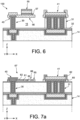
- the detection device 100 can be completed by etching the layers 37 and 38 such that the thermometric elements 56 and the MIM structures 55 form suspended membranes ( Figure 6 ).
- Layers 37 and 38 are for example eliminated by chemical attack with hydrofluoric acid (HF) in the vapor phase.
- HF hydrofluoric acid
- An HF treatment in the vapor phase is preferred here to chemical etching in the liquid phase which could lead to a collapse of the suspended structures of the infrared thermal detectors 57 due to the surface tension of the liquid which would be exerted on them.
- Hydrofluoric acid in the vapor phase is known to perfectly eliminate undoped silicon oxide such as USG from layer 37 and SiO 2 from layer 38.
- HF is inert with respect to the alumina layer 32 which therefore constitutes an effective barrier to prevent the propagation of the chemical attack towards the IMD dielectric layers of the lower electrical interconnection levels.
- the HF is inert with respect to the layers 50, 51, 52, 53, 54 present in the infrared thermal detectors 57, respectively in amorphous silicon, in alumina, in aluminum, in an amorphous alloy of silicon and germanium and aluminum.
- the electrically conductive vias 30 and 31 are also made from materials such as copper or tungsten which are not very sensitive to hydrofluoric acid and which can also be encapsulated by protective layers. More resistant to HF, such as titanium nitride or a titanium-tungsten alloy or silicon carbide.
- Portions of materials from layers 37 and 38 are kept around the vias 31 in order to improve the mechanical robustness of the second electrical contacts 41. This also makes it possible to reduce the necessary etching time, and therefore the cost linked to this etching. These portions are preserved because the size of these vias along the X or Y axis, for example equal to approximately 100 ⁇ m, is much greater than that along the Z axis, for example between approximately 1 and 10 ⁇ m.
- the infrared detection device 100 thus obtained comprises one or more infrared thermal detectors 57 made in a suspended manner above the etching stop layer 32 and above the penultimate level of electrical interconnections 20.
- empty space 16 surrounds each via 30, that is to say that each via 30 is not in contact with dielectric material of the inter-metal dielectric layer 37 located between the penultimate and the last level d electrical interconnections.
- Each empty space 16 extends under each infrared thermal detector 57 and thus forms an optical cavity of each infrared thermal detector 57.
- the infrared thermal detector(s) 57 are therefore produced at the same level as the or the connection pads 41 formed by the last level of electrical interconnections, that is to say that the distance separating the etching stop layer 32 from an infrared thermal detector 57 is substantially equal to the distance separating a pad connection 41 of this etching stop layer 32.
- a resistive layer 61 for example metallic or based on a doped semiconductor, whose resistivity - thickness couple is adapted to optimize the absorption of infrared radiation by resistive coupling of the electrons of this layer, is deposited on the first layer 60.
- a photolithography and etching step is implemented in order to fragment the resistive layer 61 into different portions 65 so as to create, on the one hand, absorbent elements formed by remaining portions of the resistive layer 61 and, on the other hand, elements thermometric sensors 66 between said remaining portions, where the resistive layer 61 has been eliminated.
- the second layer 62 makes it possible to obtain a structure of symmetrical layers which makes it possible on the one hand to compensate for the mechanical constraints which result from the bimetallic effect between the layers 60 and 61, and on the other hand to protect completely the resistive layer 61, which is generally very thin, with respect to the chemical etching in an HF medium subsequently used to form the suspended membranes of the infrared thermal detectors 67.
- Each infrared thermal detector 67 comprising thermometric elements 66, resistive elements 65 and one or more first electrical contacts 40 is defined by photolithography and etching of layers 60 and 62.
- FIG. 7b shows a top view of an example of such a thermal detector 67, comprising a central element 63 formed in the temperature-sensitive material and comprising the resistive elements 65 in the form of resistive ribbons, for example metallic.
- the spaces between the resistive ribbons form an overall thermometric element formed of several unitary thermometric elements 66 connected in series by the intermediate resistive ribbons of lower resistance.
- Other shapes are possible to form the resistive elements 65, such as for example interdigitated combs comprising segments arranged in perpendicular directions to respectively produce the teeth and the back of the combs.
- the central element 63 is extended by portions of reduced sections 64, formed by parts of the stack of layers 60, 61 and 62 and each connected by their end to a first electrical contact 40.
- thermometric elements 65 infrared energy is absorbed by the elements 65 and transformed into heat which is transmitted to the thermometric elements 66.
- a temperature gradient is then established between the central element 63 which heats up and the ends of the portions of reduced section 64 in shunt thermal with the substrate via the electrical links formed by the vias 30.
- the electrical resistance of the thermometric patterns 66 is modified and its measurement reflects the amplitude of the infrared signal captured by the elements 65.
- the rest of the process for processing the second electrical contacts 41 and for obtaining the suspended membranes is identical to that already described for the detection device 100 according to the first embodiment, and corresponds in particular to the etching of layers 37 and 38 such as thermal detectors 67 include suspended membranes.
- the sectional view of the figure 8 shows that the infrared thermal detector 67 is formed in particular of a fragmented resistive film 61, surrounded by dielectric layers 60 and 62 transparent to infrared, all suspended in a dielectric medium.
- the absorption of a continuous resistive film separating two infinite dielectric half-spaces is equal to 50% whatever the wavelength, if the ratio of the resistivity ⁇ to the thickness e of the resistive layer 61 is close to 60. ⁇ , or 188 ⁇ , and if we assume that the refractive index and the extinction coefficient of the resistive layer 61 are equal, which is generally the case in the field infrared wavelengths.
- This resistance of 188 ⁇ can be obtained by producing the resistive layer 61 based on TiN deposited by cathode sputtering, with a resistivity equal to approximately 150 ⁇ .cm, with a thickness equal to approximately 16 nm and fragmented in such a way that its rate of coverage (surface of the resistive elements 65 relative to the total surface of the central element 63, in the plane (X;Y)) is approximately 50% to obtain an apparent resistivity of 300 ⁇ .cm.
- the infrared detection device 200 thus obtained comprises one or more infrared thermal detectors 67 produced in a manner suspended above the etching stop layer 32 and above the front last level of electrical interconnections 20.
- An empty space 16 surrounds each via 30, that is to say that each via 30 is not in contact with dielectric material of the inter-metal dielectric layer 37 located between the The penultimate and final level of electrical interconnections.
- Each empty space 16 extends under each infrared thermal detector 67 and thus forms an optical cavity of each infrared thermal detector 67.
- the infrared thermal detector(s) 67 are made at the same level as the connection pad(s) 41 formed by the last level of electrical interconnections, that is to say that the distance separating the etching stop layer 32 of an infrared thermal detector 67 is substantially equal to the distance separating a connection pad 41 from this etching stop layer 32.
- the absorption of the detection device 200 can be improved beyond 50% by providing for coupling a reflective element 69 positioned opposite and under each of the thermal detectors 67, of substantially identical surface. to the thermal detector 67 and spaced from the detector by a distance equal to a quarter of the wavelength intended to be measured.
- a reflecting element 69 is produced by means of a portion of the metal line 21 of the penultimate interconnection level 20.
- the Figure 9 relates to a copper damascene back-end technology, it is possible to produce, with the same advantage of improving absorption, the reflector element 69 in aluminum back-end technology, to the extent that the copper and the aluminum have high and similar reflective qualities in the infrared range.
- the sectional view of the Figure 9 shows that the infrared thermal detector 67 is formed, from bottom to top starting from the penultimate interconnection level 20 of the CMOS substrate, of a metallic reflector 69 formed in the interconnection level 20, of two dielectric layers 29 , 32 of small thickness, of the empty space 16 forming an air blade 16 of thickness preferably between approximately 2 ⁇ m and 2.5 ⁇ m by adjusting the thickness of the sacrificial layer 37, of a stack of layers comprising at least one fragmented resistive layer 61, the other layers of dielectric nature 60, 62 being transparent to infrared.
- the reflector 69, the air blade 16 and the fragmented semi-absorbent resistive layer 61 form a quarter-wave interference cavity which has a resonance peak for a wavelength equal to 4 times the thickness of the blade d 'air 16, in other words 10 ⁇ m and therefore well suited to thermal imaging. Under these conditions and according to Maxwell's laws, this cavity can be designed to obtain absorption close to 100% near 10 ⁇ m wavelength if the ratio ⁇ /e of the resistivity to the thickness of the resistive layer 61 is close to 120. ⁇ , or 377 ⁇ .
- This resistance can be obtained by producing the resistive layer 61 based on titanium nitride deposited by cathode sputtering, with a resistivity equal to approximately 150 ⁇ .cm, with a thickness equal to 8 nm and fragmented in such a way that its filling rate (surface resistive elements 65 relative to the total surface of the central element 63, in the plane (X;Y)) or approximately 50% to obtain an apparent resistivity of 300 ⁇ .cm.
- the fragmentation of the resistive layer 61 must also comply with design rules such that the pattern of the fragmented elements is repeated in a step typically between once and half the wavelength of interest to obtain a higher average absorption. at 90%. Strips of width equal to about 2.5 ⁇ m spaced about 2.5 ⁇ m up to bands of about 4 ⁇ m spaced about 4 ⁇ m apart are suitable for detecting radiation between about 8 ⁇ m and 12 ⁇ m.
- This first alternative embodiment coupling reflective elements formed in the interconnection level 20 of the CMOS substrate to the thermal detectors can also be applied to the first embodiment previously described.
- FIG. 10 represents the detection device 200 obtained according to a second variant of the second embodiment, in which an extension 42 of the first electrical contacts 40 is produced.
- the extension 42 of the first electrical contact 40 formed from layers 44, 45 and 46 also forming the first electrical contact 40, serves both as electrical connection and thermal insulation between the first electrical contact 40 and the element thermometric of the thermal detector 67 which is electrically connected to the via 30 via the first electrical contact 40 and the extension 42.
- the extension 42 is advantageously provided with an elongated form factor so as to reproduce the section element reduced 64 previously described.
- the element of reduced section thus formed is devoid of layers 60, 61 and 62 in favor of layers 44, 45 and 46, which makes it possible to significantly reduce its section because layers 60 and 62 of the material sensitive to the temperature are generally provided thick to improve the signal-to-noise ratio of the thermometric element.
- the embodiments and variants described above are advantageous because three photolithography steps are sufficient to construct infrared thermal detectors in the form of micro-bolometers on a CMOS substrate at the last level of electrical interconnections and in which electrical links are provided, at least in the penultimate level of electrical interconnections, to connect the terminals of the thermal detectors to the inputs of the read circuit 12 formed in the CMOS substrate. This results in a very advantageous manufacturing cost.
- the following embodiments and variants make it possible to improve the detection performance of the detection device, using a greater number of photolithography steps.
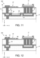
- FIG 11 represents the variant previously described in connection with the Figure 9 , in which an additional photolithography level is provided to define and open, by etching, windows in the layers 29, 32 with the aim of clearing the upper face of the reflector 69 of any superficial dielectric layers capable of absorbing infrared energy and to consequently degrade the optical quality of the quarter-wave interference cavity formed between the thermal detector 67 and the reflector 69.
- This photolithography and etching operation occurs between the step of deposition of the etching stop layer 32. and the step of depositing the sacrificial layer 37.
- This variant advantageously applies to the case where a thermal detector is provided in association with a quarter-wave cavity and a reflector.
- these photolithography and etching steps are implemented to eliminate only the part of the etching stop layer 32 at the level of the reflector 69 and not the part of the dielectric layer 29 placed facing the reflector 69 forming a copper diffusion barrier, particularly during heat treatments which accompany the rest of the process.
- the part of the dielectric layer 29 can be eliminated from the surface of the reflector 69 during a subsequent step implemented just after the operation of eliminating the layers 37, 38 by acid attack in an HF vapor medium. , a stage beyond which the heat treatments are moderate, typically below 200°C.
- Hydrofluoric acid in the vapor phase is known to perfectly eliminate silicon oxide such as USG from layer 37 and silicon dioxide from layer 38. On the other hand it creates solid nitrided residues when in contact with a silicon nitride such as that of layer 29.
- a silicon nitride such as that of layer 29.
- By sufficiently prolonging its exposure to HF vapors it is possible to transform the material of the dielectric layer 29 over its entire thickness, into nitrided residues located in the zones where the etching stop layer 32 has been previously etched. Apart from these opening zones and a small extension under layer 32 at the periphery of these opening zones, the silicon nitride of layer 29 is preserved in its state thanks to the protection provided by the layer 32.
- nitrided residues are then advantageously eliminated by a sublimation heat treatment, for example for approximately 30 minutes at a temperature equal to approximately 180° C. under a pressure of approximately 10 Pascal, which is preferred to avoid any transition by a liquid phase which could collapse suspended structures due to the surface tensions which would develop.
- an additional photolithography level making it possible to define, by local etching of the layer 60 of temperature-sensitive material, an electrical contact zone additional between the resistive layer 61 and the upper layer 46 of one of the first electrical contacts 40.
- Such an electrical contact zone makes it possible to advantageously reduce the access resistance to the thermal detector 67 and to consequently increase its thermal sensitivity.
- This additional photolithography step is inserted between the deposition of layer 60 and the deposition of resistive layer 61.
- the electrical contact can be formed by the extension of layer 61 in the opening created by the etching of layer 60 until 'in contact with layer 46, as shown in the Figure 11 .
- Another variant can consist of forming an additional electrical contact zone using an additional metallic layer deposited after the resistive layer 61 and defined by photolithography so as to cover the opening created in the layer 60, the additional metallic layer being etched outside this zone of covering to limit its size to the only surface necessary for good resumption of electrical contact between layers 46 and 61.
- the nature and thickness of the additional metal layer are chosen so as to have a continuous section between the top and the bottom of the opening created in layer 60.
- the infrared thermal detector 67 is formed of a central element 63 composed, in addition to resistive elements 65 for example in the form of metal ribbons, of thermometric elements 66 in the form of three layers 60, 62, 76 d 'a temperature-sensitive material whose total thickness is significantly greater than the sum of the thicknesses of 60 and 62. This results in a reduction in the electrical noise of the thermometric elements 66 according to a law inversely proportional to the thickness of the thermometric elements 66.
- the temporary layer 75 is automatically removed during a subsequent step of etching at least part of the first sacrificial layer, so that the infrared thermal detector 67 is also formed of portions of reduced sections 64 in the form of three stacked layers 60, 61, 62 whose thickness is significantly less than the thickness of the central element 63. This results in a reduction in the thermal conductance of the elements 64 and consequently better thermal insulation of the central element 63 and a gain in sensitivity of the thermal detector infrared 67.
- thermal detectors may be suitable insofar as none of the visible faces of these detectors contain materials likely to be attacked by the etching used to remove layers 37 and 38, such as chemical etching in the medium.
- HF chemical etching in the medium.
- detectors include for example silicon, germanium, aluminum (alloyed or not with copper and/or silicon), tungsten, titanium nitride, a titanium alloy such as TiAl or TiW, molybdenum silicide, copper, gold, nickel, chromium, ruthenium, copper-tin alloy, alumina, silicon carbide, amorphous carbon, aluminum trifluoride, or aluminum nitride.
- the step of etching layer 50 (or layers 60 and 62 in the case of the second embodiment) defining and separating the thermal detectors from each other, is implemented in order to preferentially spare the portions of this layer 50 covering the second electrical contacts 41.
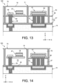
- a second sacrificial dielectric layer 70 for example and preferably of the same nature as the first sacrificial layer 37 (in USG for example) is deposited above the elements previously produced, and planarized.
- the thickness of this second sacrificial layer 70 is for example between approximately 1 ⁇ m and 3 ⁇ m.
- Trenches 71 are defined by photolithography and etched in layers 70, 38 and 37, opening for example on the etching stop layer 32, or possibly on layers lower than layer 32. Trenches 71 are defined such that they form closed perimeters when they surround one or more thermal detectors. Outside the area where the thermal detectors are formed, trenches can be provided but not necessarily, their perimeter can be either open or closed. On the example of the Figure 13 , trenches 71 are also provided on either side of a second electrical contact 41.
- An encapsulation layer 72 transparent to infrared is then deposited using a deposition technique adapted to obtain good coverage of the vertical sides of the trenches 71. It may for example be a layer of amorphous silicon produced by CVD or by iPVD, with a thickness typically between approximately 400 nm and 1200 nm when measured on a flat surface.
- the deposition of the encapsulation layer 72 on a surface structured by trenches 71 whose perimeter is closed leads to the formation of hermetic capsules, made with the material of the encapsulation layer 72 and forming, in contact with the substrate, volumes in which the thermal detectors are enclosed.
- the deposition of the encapsulation layer 72 can also form capsules outside the zone of the thermal detectors, for example around the second electrical contacts 41.
- Orifices 73, or openings, are then produced by photolithography and etching in the layer encapsulation 72.
- Each orifice 73 can be square, rectangular, circular or oblong, its small dimension typically being between approximately 200 nm and 600 nm.
- At least one orifice 73 per closed perimeter surrounding at least one thermal detector is provided. More advantageously, the orifices 73 can be made through the layer encapsulation 72 with a repetition pitch of approximately 10 ⁇ m.
- the capsules surrounding the second electrical contacts do not have an orifice.
- the sacrificial layers 37, 70 and the layer 38 are eliminated, by a chemical attack in HF vapor, forming cavities 18 containing the thermal detectors 57, 67 as well as the empty spaces 16, via the orifices 73.
- the reactive agents and the products of the chemical reaction, all in gaseous form, are respectively introduced and evacuated via the orifices 73.
- the propagation of the chemical etching by HF is controlled vertically by the presence of the barrier layer 32 and by the material of the encapsulation layer 72 in the other directions.
- a blocking layer 74 transparent to infrared is deposited, fulfilling on the one hand a function of closing the orifices 73 to obtain hermetically closed cavities around the thermal detectors 57, 67 and on the other hand an anti-reflective function to promote the transmission of infrared radiation through the encapsulation layer 72, towards the thermal detectors 57, 67.
- the blocking layer 74 comprises, for example, alternating deposits of germanium and zinc sulphide, thus forming a good quality anti-reflective layer for infrared wavelengths between approximately 8 ⁇ m and 12 ⁇ m.
- the blocking layer 74 can be produced by a technique of deposition of thin layers under vacuum such as for example the evaporation under vacuum of a source heated by an electron beam (EBPVD).
- EBPVD electron beam
- thermal detectors of infrared radiation enclosed inside cavities 18 hermetically closed by layers transparent to infrared and under reduced atmospheric pressure.
- These thermal detectors 57, 67 are therefore functional as is without it being necessary to integrate them into a vacuum housing. This results in an advantageous manufacturing cost.
- a final photolithography step makes it possible to open the connection pads of the detection device 100 formed by the second electrical contacts 41 by localized etching of layers 74, 72, 70, possibly layers 48 and 50 if the latter have been spared on the surface of second electrical contacts 41 in a previous step, to open onto the surface of the layer 47 of these second electrical contacts 41.
- the hermetic confinement, or encapsulation, of the thermal detectors 57, 67 can also be carried out as described for example in the document US 5,895,233 .
- This confinement method is described below in connection with the detection device 200 according to the second embodiment. However, such confinement can be achieved with the detection device 100 according to the first embodiment.
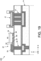
- a second substrate 90 is provided chosen from an infrared transparent material, preferably made of silicon, which is sealed with the first substrate 10 on which are formed the thermal detectors 57, 67 connected to the CMOS reading circuit 12, the first and the second substrate being spaced from one another so as to form a hermetic cavity around the thermal detectors.
- a step of etching the layers 60 and 62 defines and separates the thermal detectors from each other and preferentially opens the layers 60, 62 on the surface of the second electrical contacts 41.
- a dielectric protective layer 81 for example and preferably of the same nature as the sacrificial layer 37 (in USG for example), is deposited then planarized.
- the thickness of the protective dielectric layer 81 is typically between approximately 0.5 ⁇ m and 2 ⁇ m.
- a trench zone 82 forming a closed perimeter around one or more thermal detectors intended to be encapsulated, is defined by photolithography, then etched through layers 81, 38 and 37.
- a layer 83 is then deposited. used as an adhesion layer and as a copper diffusion barrier, then to the deposition of a copper layer 84 which serves both as a cathode and a seed layer for the electrolytic growth of a copper layer 85 followed by an electrolytic layer of tin 86.
- Layer 83 can be provided with an alloy of titanium and tungsten (TiW), deposited by cathode sputtering.
- layers 85, 86 is limited to the surface of trenches 82, for example by extending a photosensitive resin specifically designed to localize electrolytic growth reactions, on the surface of the first substrate already covered with layer 84.
- the photosensitive resin is then re-opened above the trench 82 to discover the germination layer 84 where electrolytic growth can form.
- Cleaning steps then make it possible to eliminate the photosensitive resin and the metal layers 83, 84 from the flat surface of the layer 81 (chemical cleaning and chemical mechanical polishing).
- the sacrificial layers 37, 81 and the dielectric layer 38 are eliminated by acid attack in an HF vapor medium.
- the vertical propagation of the chemical attack is controlled by the presence of the etch stop layer 32 which protects the IMD layers from the lower electrical interconnection levels.
- the propagation of the chemical attack under the connection pads is relatively small given their dimension (from 100 ⁇ m to 150 ⁇ m on each side) which is much greater than the thickness of layer 37 (from 1 ⁇ m to 5 ⁇ m).
- Layers 83, 84, 85, 86, respectively made of TiW, copper, electrolytic copper and tin, are resistant to hydrofluoric acid and therefore remain in place.
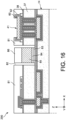
- the first substrate 10 then comprises on the surface connection pads formed by the second electrical contacts 41 and suspended membranes of the thermal detectors 67 surrounded by metal cords 88 intended to be sealed with other metal cords 98 made on a second substrate 90.
- the first face of the substrate 90 also includes recesses in some of which the elements 91, 97 are formed.
- the metal cords 98 are for their part formed on areas of the second substrate 90 located outside the recesses.
- a second anti-reflection layer 92, or possibly a more selective optical filter, is also provided on the second face of the substrate 90.
- a second substrate 90 ready to be sealed with a first substrate 10 and provided in such a way that we have opposite the metal cords 98 and 88, the anti-reflective treatment 91 with the suspended membranes of the thermal detectors 57, 67, a recess 99 facing the second electrical contacts 41.
- the recess 99 is provided to be able to cut with a saw the area of the substrate 90 facing the second electrical contacts 41, without damaging them (step not shown) .
- the operation of sealing the substrates 10 and 90 then consists of aligning the two substrates so as to bring their sealing cord 88 and 98 into contact with each other, then heating the assembly to reach a temperature greater than the melting temperature of tin. This results in the inter-diffusion of the tin into the copper and the formation of a copper-tin intermetallic alloy which solidifies with a melting point significantly higher than the temperature used for sealing.
- this sealing operation is carried out in a vacuum chamber so as to hermetically seal under vacuum the thermal detectors 57, 67 in hermetic cavities 96.
Landscapes
- Physics & Mathematics (AREA)
- General Physics & Mathematics (AREA)
- Spectroscopy & Molecular Physics (AREA)
- Engineering & Computer Science (AREA)
- Manufacturing & Machinery (AREA)
- Photometry And Measurement Of Optical Pulse Characteristics (AREA)
- Solid State Image Pick-Up Elements (AREA)
Claims (22)
- Infrarot-Detektionsvorrichtung (100, 200), mindestens enthaltend:- eine elektronische Leseschaltung (12), die auf und/oder in einem ersten Halbleitersubstrat (10) ausgebildet ist, und auf der mehrere Ebenen elektrischer Vernetzungen (14) angeordnet sind, so dass eine erste Ebene elektrischer Vernetzungen zwischen der elektronischen Leseschaltung (12) und einer letzten Ebene elektrischer Vernetzungen angeordnet ist;- eine Ätzsperrschicht (32), die zwischen der letzten und einer vorletzten Ebene elektrischer Vernetzungen angeordnet ist, und geeignet ist, einer Ätzung einer ersten intermetallischen dielektrischen Schicht (37), die zwischen der Ätzsperrschicht (32) und der letzten Ebene elektrischer Vernetzungen angeordnet ist, standzuhalten;- einen Infrarot-Wärmedetektor (57, 67), der durch mindestens eine erste elektrisch leitende Via (30) der letzten Ebene elektrischer Vernetzungen, die durch die Ätzsperrschicht (32) verläuft, elektrisch an die elektronische Leseschaltung (12) angeschlossen ist;- ein Anschluss-Pad (41), das aus der letzten Ebene elektrischer Vernetzungen gebildet ist, und durch mindestens eine zweite elektrisch leitende Via (31) der letzten Ebene elektrischer Vernetzungen, die durch die Ätzsperrschicht (32) verläuft, elektrisch an die elektronische Leseschaltung (12) angeschlossen ist, und geeignet ist, um von außerhalb der Infrarot-Detektionsvorrichtung (100, 200) elektrisch kontaktiert zu werden;wobei der Infrarot-Wärmedetektor (57, 67) und das Anschluss-Pad (41) jeweils um einen im Wesentlichen gleichen Abstand ungleich null voneinander von der Ätzsperrschicht (32) beabstandet sind, wobei die erste und die zweite elektrisch leitende Via (30, 31) jeweils elektrisch an den ersten und zweiten Abschnitt (21a, 21b) einer Metallleitung (21) einer vorletzten Ebene elektrischer Vernetzungen (20) angeschlossen sind, und wobei ein Leerraum (16), der in der ersten intermetallischen dielektrischen Schicht (37) gebildet ist, die erste elektrisch leitende Via (30) umgibt, und sich unter dem Infrarot-Wärmedetektor (57, 67) erstreckt,und wobei von dem Infrarot-Wärmedetektor (57, 67) und dem Anschluss-Pad (41) nur der Infrarot-Wärmedetektor (57, 67) mindestens ein absorbierendes Element (55, 65) enthält, das geeignet ist, eine Infrarotstrahlung zu absorbieren, die dazu bestimmt ist, durch den Infrarot-Wärmedetektor (57, 67) detektiert zu werden, und mindestens ein thermometrisches Element (56, 66), das mit dem absorbierenden Element (55, 65) gekoppelt ist,und wobei der Infrarot-Wärmedetektor (57, 67) eine aufgehängte Membran enthält, die sich in dem Abstand ungleich null von der Ätzsperrschicht (32) befindet, wobei die aufgehängte Membran das absorbierende Element (55, 65) und das thermometrische Element (56, 66) enthält.
- Infrarot-Detektionsvorrichtung (100, 200) nach Anspruch 1, wobei die elektronische Leseschaltung (12) eine Vielzahl von elektronischen Vorrichtungen vom Typ MOS enthält, die auf und/oder im ersten Halbleitersubstrat (10) ausgebildet sind, wobei die vorletzte Ebene elektrischer Vernetzungen (20) dritte elektrisch leitende Vias (22) enthält, die in einer zweiten intermetallischen dielektrischen Schicht (27) ausgebildet sind und mindestens erste Abschnitte (21a) der Metallleitung (21) elektrisch an die elektronischen Vorrichtungen vom Typ MOS anschließen, und wobei die Ätzsperrschicht (32) auf der zweiten intermetallischen dielektrischen Schicht (27) angeordnet ist.
- Infrarot-Detektionsvorrichtung (100, 200) nach Anspruch 2, wobei die Metallleitung (21) und die dritten elektrisch leitenden Vias (22) auf mindestens demselben Material basieren wie das der ersten elektrisch leitenden Via (30).
- Infrarot-Detektionsvorrichtung (100, 200) nach einem der vorhergehenden Ansprüche, wobei mindestens ein dritter Abschnitt (69) der Metallleitung (21) gegenüber dem Infrarot-Wärmedetektor (57, 67) angeordnet ist und geeignet ist, mindestens einen Teil einer Infrarotstrahlung zu reflektieren, die dazu bestimmt ist, vom Infrarot-Wärmedetektor (57, 67) detektiert zu werden.
- Infrarot-Detektionsvorrichtung (100, 200) nach Anspruch 4, wobei der dritte Abschnitt (69) der Metallleitung (21) nicht von der Ätzsperrschicht (32) bedeckt ist.
- Infrarot-Detektionsvorrichtung (100) nach einem der vorhergehenden Ansprüche, wobei der Infrarot-Wärmedetektor (57) einen Metall-Isolator-Metall-Stapel (55) enthält, der geeignet ist, eine Infrarotstrahlung zu absorbieren, die dazu bestimmt ist, vom Infrarot-Wärmedetektor (57) detektiert zu werden, und mindestens einen Abschnitt des Materials (56), dessen Resistivität sich in Abhängigkeit von der Temperatur ändert, und thermisch mit dem Metall-Isolator-Metall-Stapel (55) gekoppelt ist und elektrisch an die erste elektrisch leitende Via (30) angeschlossen ist.
- Infrarot-Detektionsvorrichtung (200) nach einem der Ansprüche 1 bis 5, wobei der Infrarot-Wärmedetektor (67) eine Vielzahl von Resistivitätsabschnitten (65) enthält, die geeignet sind, eine Infrarotstrahlung zu absorbieren, die dazu bestimmt ist, durch den Infrarot-Wärmedetektor (67) detektiert zu werden, und eine Vielzahl von Abschnitten (66) des Material, dessen Resistivität sich in Abhängigkeit von der Temperatur ändert, wobei mindestens einer der Abschnitte (66) des Materials, dessen Resistivität sich in Abhängigkeit von der Temperatur ändert, elektrisch an die erste elektrisch leitende Via (30) angeschlossen ist.
- Infrarot-Detektionsvorrichtung (100, 200) nach einem der vorhergehenden Ansprüche, ferner mindestens einen ersten elektrischen Kontakt (40) enthaltend, der auf der ersten elektrisch leitenden Via (30) angeordnet ist, wobei der Infrarot-Wärmedetektor (57, 67) über den elektrischen Kontakt (40) elektrisch an die erste elektrisch leitende Via (30) angeschlossen ist.
- Infrarot-Detektionsvorrichtung (100, 200) nach einem der vorhergehenden Ansprüche, wobei der Infrarot-Wärmedetektor (57, 67) in einem Hohlraum (18) eingekapselt ist, der mindestens durch eine Verkapselungsschicht (72) begrenzt ist, die auf einem Material basiert, das für eine Infrarotstrahlung transparent ist, die dafür bestimmt ist, durch den Infrarot-Wärmedetektor (57, 67) detektiert zu werden, und durch die Ätzsperrschicht (32).
- Infrarot-Detektionsvorrichtung (100, 200) nach einem der Ansprüche 1 bis 8, wobei der Infrarot-Wärmedetektor (57, 67) in einem Hohlraum (96) eingekapselt ist, der mindestens begrenzt ist durch ein zweites Substrat (90), die Ätzsperrschicht (32) und ein Metallband (88), das das zweite Substrat (90) mit der Ätzsperrschicht (32) fest verbindet, wobei das zweite Substrat (90) auf mindestens einem Material basiert, das für eine Infrarotstrahlung transparent ist, die dazu bestimmt ist, durch den Infrarot-Wärmedetektor (57, 67) detektiert zu werden.
- Infrarot-Detektionsvorrichtung (100, 200) nach einem der vorhergehenden Ansprüche, eine Vielzahl von Infrarot-Wärmedetektoren (57, 67) enthaltend, die eine Matrix der Pixel der Infrarot-Detektionsvorrichtung (100, 200) bilden, wobei jeder Infrarot-Wärmedetektor (57, 67) durch mindestens eine erste elektrisch leitende Via (30) elektrisch an die elektronische Leseschaltung (12) angeschlossen ist.
- Verfahren zur Bildung einer Infrarot-Detektionsvorrichtung (100, 200), mindestens die Durchführung der Schritte enthaltend:- Bildung mehrerer Ebenen elektrischer Vernetzungen (14) auf einer elektronischen Leseschaltung (12), die auf und/oder in einem ersten Halbleitersubstrat (10) ausgebildet ist und einen Stapel bildet, der von einer ersten Ebene elektrischer Vernetzungen zu einer vorletzten Ebene elektrischer Vernetzungen reicht;- Abscheidung einer Ätzsperrschicht (32) auf der vorletzten Ebene elektrischer Vernetzungen;- Abscheidung einer ersten intermetallischen dielektrischen Schicht (37) auf der Ätzsperrschicht (32), wobei die erste intermetallische dielektrische Schicht (37) mindestens ein mineralisches Material enthält, das geeignet ist, selektiv in Bezug auf die Ätzsperrschicht (32) geätzt zu werden;- Bildung, auf der ersten intermetallischen dielektrische Schicht (37), einer letzten Ebene elektrischer Vernetzungen, die mindestens ein Anschluss-Pad (41) bildet, das durch mindestens eine zweite elektrisch leitende Via (31) der letzten Ebene von elektrischen Vernetzungen, die durch die erste intermetallische dielektrische Schicht (37) und die Ätzsperrschicht (32) verläuft, elektrisch an die elektronische Leseschaltung (12) angeschlossen ist, wobei das Anschluss-Pad (41) geeignet ist, von außerhalb der Infrarot-Detektionsvorrichtung (100, 200) elektrisch kontaktiert zu werden, und von mindestens einem Infrarot-Wärmedetektor (57, 67), der durch mindestens eine erste elektrisch leitende Via (30) der letzten Ebene elektrischer Vernetzungen, die durch die erste intermetallische dielektrische Schicht (37) und die Ätzsperrschicht (32) verläuft, elektrisch an die elektronische Leseschaltung (12) angeschlossen ist, wobei die erste und die zweite elektrisch leitende Via (30, 31) jeweils elektrisch an die ersten und zweiten Abschnitte (21a, 21b) einer Metallleitung (21) der vorletzten Ebene elektrischer Vernetzungen (20) angeschlossen sind, und wobei der Infrarot-Wärmedetektor (57, 67) und das Anschluss-Pad (41) jeweils um einen im Wesentlichen gleichen Abstand ungleich null voneinander von der Ätzsperrschicht (32) beabstandet sind;- Ätzung mindestens eines Teils der ersten intermetallischen dielektrischen Schicht (37), die zwischen der elektronischen Leseschaltung (12) und dem Infrarot-Wärmedetektor (57, 67) angeordnet ist und einen Leerraum (16) bildet, der die erste elektrisch leitende Via (30) umgibt und sich unter dem Infrarot-Wärmedetektor (57, 67) erstreckt,und wobei unter dem Infrarot-Wärmedetektor (57, 67) und dem Anschluss-Pad (41) nur der Infrarot-Wärmedetektor (57, 67) mindestens ein absorbierendes Element (55, 65) enthält, das geeignet ist, eine Infrarotstrahlung zu absorbieren, die dazu bestimmt ist, vom Infrarot-Wärmedetektor (57, 67) detektiert zu werden, und mindestens ein thermometrisches Element (56, 66), das mit dem absorbierenden Element (55, 65) gekoppelt ist,und wobei der Infrarot-Wärmedetektor (57, 67) eine aufgehängte Membran enthält, die sich in dem Abstand ungleich null von der Ätzsperrschicht (32) befindet, wobei die aufgehängte Membran das absorbierende Element (55, 65) und das thermometrische Element (56, 66) enthält.
- Verfahren nach Anspruch 12, wobei die elektronische Leseschaltung (12) eine Vielzahl von elektronischen Vorrichtungen vom Typ MOS enthält, die auf und/oder im ersten Halbleitersubstrat (10) ausgebildet sind, und wobei die vorletzte Ebene elektrischer Vernetzungen (20) dritte elektrisch leitende Vias (22) enthält, die in einer zweiten intermetallischen dielektrischen Schicht (27) ausgebildet sind und mindestens erste Abschnitte (21a) der Metallleitung (21) elektrisch an die elektronischen Vorrichtungen vom Typ MOS anschließen, und wobei die Ätzsperrschicht (32) auf der zweiten intermetallischen dielektrischen Schicht (27) abgeschieden ist.
- Verfahren nach Anspruch 13, wobei die Metallleitung (21) und die dritten elektrisch leitenden Vias (22) auf mindestens demselben Material wie das der ersten elektrisch leitenden Via (30) basieren, und wobei die zweite intermetallische dielektrische Schicht (27) auf demselben mineralischen Material wie das der ersten intermetallischen dielektrischen Schicht (37) basiert.
- Verfahren nach einem der Ansprüche 12 bis 14, wobei mindestens ein dritter Abschnitt (69) der Metallleitung (21) gegenüber dem Infrarot-Wärmedetektor (57, 67) angeordnet ist und geeignet ist, mindestens einen Teil einer Infrarotstrahlung zu reflektieren, die dazu bestimmt ist, vom Infrarot-Wärmedetektor (57, 67) detektiert zu werden.
- Verfahren nach Anspruch 15, ferner zwischen dem Schritt der Abscheidung der Ätzsperrschicht (32) und dem Schritt der Abscheidung der ersten intermetallischen dielektrischen Schicht (37) einen Schritt der Ätzung eines Teils der Ätzsperrschicht (32) enthaltend, der den dritten Abschnitt (69) der Metallleitung (21) bedeckt.
- Verfahren nach einem der Ansprüche 12 bis 16, wobei die Bildung des Infrarot-Wärmedetektors (57) die Bildung eines Metall-Isolator-Metall-Stapels (55) enthält, der geeignet ist, eine Infrarotstrahlung zu absorbieren, die dazu bestimmt ist, vom Infrarot-Wärmedetektor (57) detektiert zu werden, und die Bildung von mindestens einem Abschnitt des Materials (56), dessen Resistivität sich in Abhängigkeit von der Temperatur ändert, und thermisch mit dem Metall-Isolator-Metall-Stapel (55) gekoppelt ist und elektrisch an die erste elektrisch leitende Via (30) angeschlossen ist.
- Verfahren nach einem der Ansprüche 12 bis 16, wobei die Bildung des Infrarot-Wärmedetektors (67) die Bildung einer Vielzahl von Resistivitätsabschnitten (65) enthält, die geeignet sind, eine Infrarotstrahlung zu absorbieren, die dazu bestimmt ist, vom Infrarot-Wärmedetektor (67) detektiert zu werden, und die Bildung einer Vielzahl von Abschnitten (66) von Material, dessen Resistivität sich in Abhängigkeit von der Temperatur ändert, wobei mindestens einer der Abschnitte (66) von Material, dessen Resistivität sich in Abhängigkeit von der Temperatur ändert, elektrisch an die erste elektrisch leitende Via (30) angeschlossen ist.
- Verfahren nach einem der Ansprüche 12 bis 18, ferner zwischen dem Schritt der Abscheidung der ersten intermetallischen dielektrischen Schicht (37) und dem Schritt der Bildung des Infrarot-Wärmedetektors (57, 67) die Bildung von mindestens einem ersten elektrischen Kontakt (40) auf der ersten elektrisch leitenden Via (30) enthaltend, wobei der Infrarot-Wärmedetektor (57, 67) über den elektrischen Kontakt (40) elektrisch an die erste elektrisch leitende Via (30) angeschlossen ist.
- Verfahren nach einem der Ansprüche 12 bis 19, ferner zwischen dem Schritt der Bildung des Infrarot-Wärmedetektors (57, 67) und dem Schritt der Ätzung mindestens eines Teils der ersten intermetallischen dielektrischen Schicht (37) die Durchführung der Schritte enthaltend:- Abscheidung einer Opferschicht (70), die mindestens den Infrarot-Wärmedetektor (57, 67) bedeckt, wobei die Opferschicht (70) mindestens ein mineralisches Material enthält, das geeignet ist, selektiv in Bezug auf die Ätzsperrschicht (32) geätzt zu werden;- Ätzung mindestens einer Schneise (71) durch mindestens die erste intermetallische dielektrische Schicht (37) und die Opferschicht (70) hindurch, und die Abschnitte der ersten intermetallischen dielektrischen Schicht (37) und der Opferschicht (70) begrenzend;- Abscheidung, in der Schneise (71) und auf dem Abschnitt der Opferschicht (70), von mindestens einer Verkapselungsschicht (72), die auf einem Material basiert, das transparent ist für eine Infrarotstrahlung, die dazu bestimmt ist, durch den Infrarot-Wärmedetektor (57, 67) detektiert zu werden;- Bildung von mindestens einer Öffnung (73) durch die Verkapselungsschicht (72) hindurch;wobei der Schritt der Ätzung mindestens eines Teils der ersten intermetallischen dielektrischen Schicht (37) über die Öffnung (73) erfolgt und die Abschnitte der ersten intermetallischen dielektrischen Schicht (37) und der Opferschicht (70) entfernt, so dass der Infrarot-Wärmedetektor (57, 67) in einem Hohlraum (18) eingekapselt ist, der mindestens durch die Verkapselungsschicht (72) und die Ätzsperrschicht (32) begrenzt ist,und ferner, nach dem Ätzschritt, die Durchführung eines Schritts der Verschließung der Öffnung (73) enthält.
- Verfahren nach einem der Ansprüche 12 bis 19, ferner zwischen dem Schritt der Bildung des Infrarot-Wärmedetektors (57, 67) und dem Schritt der Ätzung von mindestens einem Teil der ersten intermetallischen dielektrischen Schicht (37) die Durchführung eines Schritts zur Bildung von mindestens einem Metallband (88) auf der Ätzsperrschicht (32) durch mindestens die erste intermetallische dielektrische Schicht (37) hindurch enthaltend, und ferner, nach dem Schritt der Ätzung von mindestens einem Teil der ersten intermetallischen dielektrischen Schicht (37), das feste Verbinden mindestens eines zweiten Substrat (90) mit dem Metallband (88) enthaltend, so dass der Infrarot-Wärmedetektor (57, 67) in einem Hohlraum (96) eingekapselt ist, der mindestens durch das zweite Substrat (90), die Ätzsperrschicht (32) und das Metallband (88) begrenzt ist, wobei das zweite Substrat (90) auf mindestens einem Material basiert, das für eine Infrarotstrahlung transparent ist, die dazu bestimmt ist, durch den Infrarot-Wärmedetektor (57, 67) detektiert zu werden.
- Verfahren nach einem der Ansprüche 12 bis 21, die Bildung einer Vielzahl von Infrarot-Wärmedetektoren (57, 67) enthaltend, die eine Matrix von Pixeln der Infrarot-Detektionsvorrichtung (100, 200) bilden, wobei jeder Infrarot-Wärmedetektor (57, 67) durch mindestens eine erste elektrisch leitende Via (30) elektrisch an die elektronische Leseschaltung (12) angeschlossen ist.
Applications Claiming Priority (1)
| Application Number | Priority Date | Filing Date | Title |
|---|---|---|---|
| FR1262153A FR2999805B1 (fr) | 2012-12-17 | 2012-12-17 | Procede de realisation d'un dispositif de detection infrarouge |
Publications (2)
| Publication Number | Publication Date |
|---|---|
| EP2743659A1 EP2743659A1 (de) | 2014-06-18 |
| EP2743659B1 true EP2743659B1 (de) | 2024-07-31 |
Family
ID=48128457
Family Applications (1)
| Application Number | Title | Priority Date | Filing Date |
|---|---|---|---|
| EP13197327.3A Active EP2743659B1 (de) | 2012-12-17 | 2013-12-16 | Verfahren zur Umsetzung einer Infraroterfassungsvorrichtung |
Country Status (4)
| Country | Link |
|---|---|
| US (1) | US9389125B2 (de) |
| EP (1) | EP2743659B1 (de) |
| JP (1) | JP6362323B2 (de) |
| FR (1) | FR2999805B1 (de) |
Families Citing this family (31)
| Publication number | Priority date | Publication date | Assignee | Title |
|---|---|---|---|---|
| JP5266813B2 (ja) | 2008-03-13 | 2013-08-21 | 三菱マテリアル株式会社 | エンドミル |
| JP5853586B2 (ja) | 2011-10-26 | 2016-02-09 | 三菱マテリアル株式会社 | エンドミル |
| FR3026483A1 (fr) | 2014-09-26 | 2016-04-01 | Commissariat Energie Atomique | Detecteur bolometrique a structures mim de dimensions differentes |
| FR3033045B1 (fr) | 2015-02-20 | 2020-02-28 | Commissariat A L'energie Atomique Et Aux Energies Alternatives | Dispositif de detection de rayonnement electromagnetique a structure d'encapsulation hermetique a event de liberation |
| FR3045148B1 (fr) | 2015-12-15 | 2017-12-08 | Ulis | Dispositif de detection a membranes bolometriques suspendues a fort rendement d'absorption et rapport signal sur bruit |
| WO2017103683A2 (en) * | 2015-12-16 | 2017-06-22 | Mikrosens Elektronik San. Ve Tic. A.S. Odtu Teknokent Odtu-Met Alani | Microbolometer structure |
| FR3048105B1 (fr) | 2016-02-22 | 2018-03-02 | Commissariat A L'energie Atomique Et Aux Energies Alternatives | Capteur de motifs thermiques a capsules thermo-resistives. |
| FR3048125B1 (fr) * | 2016-02-24 | 2020-06-05 | Commissariat A L'energie Atomique Et Aux Energies Alternatives | Dispositif de detection de rayonnement electromagnetique a plot de connexion electrique sureleve |
| FR3048534A1 (fr) | 2016-03-01 | 2017-09-08 | Commissariat Energie Atomique | Capteur de motifs thermiques a bolometres sous capsule(s). |
| FR3050870B1 (fr) * | 2016-04-28 | 2018-05-25 | Commissariat A L'energie Atomique Et Aux Energies Alternatives | Procede de realisation d’un dispositif de detection de rayonnement electromagnetique comportant une couche en un materiau getter |
| FR3066044B1 (fr) * | 2017-05-02 | 2020-02-21 | Commissariat A L'energie Atomique Et Aux Energies Alternatives | Detecteur de rayonnement electromagnetique, encapsule par report de couche mince. |
| FR3066017B1 (fr) | 2017-05-05 | 2019-07-05 | Commissariat A L'energie Atomique Et Aux Energies Alternatives | Dispositif pyroelectrique de detection infrarouge comportant un emetteur infrarouge de modulation |
| FR3066321B1 (fr) * | 2017-05-09 | 2019-06-14 | Commissariat A L'energie Atomique Et Aux Energies Alternatives | Procede de realisation d'un detecteur bolometrique |
| FR3070096B1 (fr) * | 2017-08-08 | 2021-09-17 | Commissariat Energie Atomique | Procede de fabrication d'un dispositif de detection a deux substrats et un tel dispositif de detection |
| EP3462149B1 (de) | 2017-09-28 | 2023-10-25 | Sensirion AG | Infrarotvorrichtung |
| US10340330B2 (en) * | 2017-10-13 | 2019-07-02 | International Business Machines Corporation | Precision BEOL resistors |
| FR3073941B1 (fr) | 2017-11-21 | 2021-01-15 | Commissariat Energie Atomique | Dispositif de detection d’un rayonnement electromagnetique a diaphotie reduite |
| CN108565310B (zh) * | 2017-12-14 | 2020-03-31 | 上海集成电路研发中心有限公司 | 一种红外探测器及其制造方法 |
| JP2019197834A (ja) * | 2018-05-10 | 2019-11-14 | 浜松ホトニクス株式会社 | 光検出素子 |
| FR3084208B1 (fr) * | 2018-07-18 | 2020-10-23 | Commissariat Energie Atomique | Dispositif de detection pyroelectrique a membrane suspendue contrainte |
| FR3087260B1 (fr) | 2018-10-12 | 2020-09-25 | Commissariat Energie Atomique | Procede de fabrication d'un dispositif de detection d'un rayonnement electromagnetique comportant un element de detection suspendu |
| FR3089685B1 (fr) | 2018-12-10 | 2020-11-20 | Ulis | Procede de realisation d’un detecteur infrarouge et detecteur infrarouge associe |
| US11661332B2 (en) * | 2019-02-20 | 2023-05-30 | Invensense, Inc. | Stiction reduction system and method thereof |
| FR3097046B1 (fr) * | 2019-06-05 | 2021-05-21 | Lynred | Microbolomètre ayant un pas de pixel réduit |
| FR3097047B1 (fr) * | 2019-06-05 | 2021-05-14 | Lynred | Microbolomètre muni d’une fonction de filtrage |
| EP4029351B1 (de) * | 2019-09-12 | 2024-04-24 | Watlow Electric Manufacturing Company | Keramisches heizelement und verfahren zur herstellung unter verwendung einer übergangsflüssigkeitsphasenbindung |
| FR3101414B1 (fr) * | 2019-09-30 | 2021-09-03 | Commissariat Energie Atomique | procede de fabrication d’un dispositif de detection de rayonnement electromagnétique comportant un materiau getter |
| US12349472B2 (en) | 2021-02-03 | 2025-07-01 | Rensselaer Polytechnic Institute | Silicon nitride waveguide coupled photodiode |
| FR3142546B1 (fr) | 2022-11-29 | 2024-12-13 | Commissariat Energie Atomique | Dispositif de détection d’un rayonnement électromagnétique et procédé de fabrication |
| FR3144280B1 (fr) | 2022-12-21 | 2025-03-07 | Commissariat Energie Atomique | Dispositif de détection d’un rayonnement electromagnétique comportant un détecteur thermique sur un substrat de lecture dont un élément électronique actif est situé au plus près du détecteur thermique |
| EP4585889A1 (de) * | 2024-01-15 | 2025-07-16 | Centre National de la Recherche Scientifique | Kern-schale-struktur für einen bolometrischen detektor |
Family Cites Families (60)
| Publication number | Priority date | Publication date | Assignee | Title |
|---|---|---|---|---|
| GB793678A (en) | 1955-07-21 | 1958-04-23 | Sperry Rand Corp | Improvements in record controlled control systems |
| EP0734589B1 (de) | 1993-12-13 | 1998-03-25 | Honeywell Inc. | Integrierte silizium-vakuum-mikropackung für infrarot-geräte |
| FR2752299B1 (fr) | 1996-08-08 | 1998-09-11 | Commissariat Energie Atomique | Detecteur infrarouge et procede de fabication de celui-ci |
| JP3040356B2 (ja) * | 1997-01-27 | 2000-05-15 | 三菱電機株式会社 | 赤外線固体撮像素子 |
| GB9710843D0 (en) * | 1997-05-28 | 1997-07-23 | Secr Defence | A thermal detector array |
| WO1999031471A1 (fr) * | 1997-12-18 | 1999-06-24 | Mitsubishi Denki Kabushiki Kaisha | Dispositif a semi-conducteur de prise d'image infrarouge |
| FR2773215B1 (fr) * | 1997-12-31 | 2000-01-28 | Commissariat Energie Atomique | Detecteur thermique bolometrique |
| EP0951068A1 (de) * | 1998-04-17 | 1999-10-20 | Interuniversitair Micro-Elektronica Centrum Vzw | Herstellungsverfahren für eine Mikrostruktur mit Innenraum |
| DE19839122A1 (de) * | 1998-08-27 | 2000-03-09 | Siemens Ag | Vor Umwelteinflüssen geschützter mikromechanischer Sensor |
| US6348650B1 (en) * | 1999-03-24 | 2002-02-19 | Ishizuka Electronics Corporation | Thermopile infrared sensor and process for producing the same |
| JP3946406B2 (ja) * | 2000-03-30 | 2007-07-18 | 株式会社東芝 | 熱型赤外線センサの製造方法 |
| AUPQ897600A0 (en) * | 2000-07-25 | 2000-08-17 | Liddiard, Kevin | Active or self-biasing micro-bolometer infrared detector |
| JP2002107224A (ja) * | 2000-09-29 | 2002-04-10 | Toshiba Corp | 赤外線センサ及びその製造方法 |
| DE10058864B4 (de) * | 2000-11-27 | 2009-06-25 | Pyreos Ltd. | Mikromechanikstruktur für integrierte Sensoranordnungen und Verfahren zur Herstellung einer Mikromechanikstruktur |
| FR2822541B1 (fr) * | 2001-03-21 | 2003-10-03 | Commissariat Energie Atomique | Procedes et dispositifs de fabrication de detecteurs de rayonnement |
| FR2833757B1 (fr) * | 2001-12-13 | 2004-11-05 | Commissariat Energie Atomique | Dispositif d'emission de lumiere et procede de fabrication d'un tel dispositif |
| JP3828443B2 (ja) * | 2002-03-22 | 2006-10-04 | 株式会社東芝 | 赤外線撮像装置及びその製造方法 |
| US6787387B2 (en) * | 2002-06-24 | 2004-09-07 | Matsushita Electric Industrial Co., Ltd. | Electronic device and method for fabricating the electronic device |
| WO2004074167A2 (en) * | 2003-02-20 | 2004-09-02 | Technion Research & Development Foundation Ltd. | A device and method for stacked multi-level uncoupled electrostatic actuators |
| DE10320357B4 (de) * | 2003-05-07 | 2010-05-12 | Perkinelmer Optoelectronics Gmbh & Co.Kg | Strahlungssensor, Wafer, Sensorarray und Sensormodul |
| DE10352001A1 (de) * | 2003-11-07 | 2005-06-09 | Robert Bosch Gmbh | Mikromechanisches Bauelement mit einer Membran und Verfahren zur Herstellung eines solchen Bauelements |
| FR2864065B1 (fr) * | 2003-12-22 | 2006-02-24 | Univ Toulouse | Utilisation de ferrites spinelles comme materiau sensible pour dispositifs bolometriques de detection de l'infrarouge. |
| GB2411521A (en) * | 2004-02-27 | 2005-08-31 | Qinetiq Ltd | Fabrication method for micro-sensor device |
| WO2005098380A1 (en) * | 2004-04-08 | 2005-10-20 | Tayfun Akin | Ultra low-cost uncooled infrared detector arrays in cmos |
| US7964926B2 (en) * | 2005-02-02 | 2011-06-21 | Samsung Electronics Co., Ltd. | Image sensing devices including image sensor chips, image sensor package modules employing the image sensing devices, electronic products employing the image sensor package modules, and methods of fabricating the same |
| FR2883417B1 (fr) * | 2005-03-16 | 2007-05-11 | Ulis Soc Par Actions Simplifie | Detecteur bolometrique, dispositif de detection infrarouge mettant en oeuvre un tel detecteur et procede de fabrication de ce detecteur |
| FR2890491B1 (fr) * | 2005-09-05 | 2008-01-25 | Commissariat Energie Atomique | Dispositif d'emission de lumiere avec couche filtrante |
| WO2007058604A1 (en) * | 2005-11-18 | 2007-05-24 | Replisaurus Technologies Ab | Master electrode and method of forming the master electrode |
| JP4792980B2 (ja) * | 2006-01-12 | 2011-10-12 | 日産自動車株式会社 | 赤外線検出素子 |
| US7442599B2 (en) * | 2006-09-15 | 2008-10-28 | Sharp Laboratories Of America, Inc. | Silicon/germanium superlattice thermal sensor |
| JP5109169B2 (ja) * | 2007-03-27 | 2012-12-26 | 日本電気株式会社 | ボロメータ型THz波検出器 |
| US7923801B2 (en) * | 2007-04-18 | 2011-04-12 | Invisage Technologies, Inc. | Materials, systems and methods for optoelectronic devices |
| JP2009174917A (ja) * | 2008-01-22 | 2009-08-06 | Oki Semiconductor Co Ltd | 赤外線検出素子、及び赤外線検出素子の製造方法 |
| US8174703B2 (en) * | 2008-05-06 | 2012-05-08 | University Of Massachusetts | Method for fabricating a sensor, a sensor, and a method for sensing |
| JP4835658B2 (ja) * | 2008-07-28 | 2011-12-14 | 日本テキサス・インスツルメンツ株式会社 | Pinフォトダイオードおよびその製造方法 |
| WO2011039797A1 (ja) * | 2009-09-29 | 2011-04-07 | パイオニア株式会社 | Memsセンサ |
| JPWO2011039798A1 (ja) * | 2009-09-29 | 2013-02-21 | パイオニア株式会社 | Memsセンサおよびこれを備えたセンサアレイ |
| JPWO2011039799A1 (ja) * | 2009-09-29 | 2013-02-21 | パイオニア株式会社 | センサアレイ |
| KR20110077451A (ko) * | 2009-12-30 | 2011-07-07 | 삼성전자주식회사 | 이미지 센서, 그 제조 방법, 및 상기 이미지 센서를 포함하는 장치 |
| KR101672737B1 (ko) * | 2010-01-21 | 2016-11-04 | 삼성전자 주식회사 | 이미지 센서 및 상기 이미지 센서를 포함하는 영상 장치 |
| JP5750827B2 (ja) * | 2010-01-26 | 2015-07-22 | セイコーエプソン株式会社 | 熱型光検出器の製造方法 |
| JP5644120B2 (ja) * | 2010-01-26 | 2014-12-24 | セイコーエプソン株式会社 | 熱型光検出器、熱型光検出装置、電子機器および熱型光検出器の製造方法 |
| JP2011153889A (ja) * | 2010-01-27 | 2011-08-11 | Seiko Epson Corp | Memsの製造方法及び熱型光検出器の製造方法並びに熱型光検出器、熱型光検出装置及び電子機器 |
| JP5589486B2 (ja) * | 2010-03-26 | 2014-09-17 | セイコーエプソン株式会社 | 焦電型光検出器、焦電型光検出装置及び電子機器 |
| JP5218460B2 (ja) * | 2010-03-26 | 2013-06-26 | セイコーエプソン株式会社 | 焦電型光検出器、焦電型光検出装置及び電子機器 |
| JP5771900B2 (ja) * | 2010-03-26 | 2015-09-02 | セイコーエプソン株式会社 | 熱型光検出器、熱型光検出装置及び電子機器 |
| FR2959013B1 (fr) | 2010-04-16 | 2012-05-11 | Commissariat Energie Atomique | Dispositif de detection de rayonnement electromagnetique a sensibilite reduite au bruit spacial |
| JP5585241B2 (ja) * | 2010-06-25 | 2014-09-10 | セイコーエプソン株式会社 | 焦電型検出器、焦電型検出装置及び電子機器 |
| JP5589605B2 (ja) * | 2010-06-25 | 2014-09-17 | セイコーエプソン株式会社 | 焦電型検出器、焦電型検出装置及び電子機器 |
| JP5521827B2 (ja) * | 2010-06-28 | 2014-06-18 | セイコーエプソン株式会社 | 焦電型検出器、焦電型検出装置及び電子機器 |
| JP5636787B2 (ja) * | 2010-07-26 | 2014-12-10 | セイコーエプソン株式会社 | 熱型光検出器、熱型光検出装置及び電子機器 |
| CA2807977A1 (en) * | 2010-07-27 | 2012-02-02 | Flir Systems, Inc. | Infrared camera architecture systems and methods |
| US8927934B2 (en) * | 2010-09-13 | 2015-01-06 | Ricoh Company, Ltd. | Thermal infrared sensor and manufacturing method thereof |
| FR2966925B1 (fr) * | 2010-11-03 | 2012-11-02 | Commissariat Energie Atomique | Detecteur infrarouge a base de micro-planches bolometriques suspendues |
| JP5870492B2 (ja) * | 2011-02-23 | 2016-03-01 | セイコーエプソン株式会社 | 熱型検出器、熱型検出装置及び電子機器 |
| JP5830877B2 (ja) * | 2011-02-24 | 2015-12-09 | セイコーエプソン株式会社 | 焦電型検出器、焦電型検出装置及び電子機器 |
| JP5879695B2 (ja) * | 2011-02-24 | 2016-03-08 | セイコーエプソン株式会社 | 焦電型検出器、焦電型検出装置及び電子機器 |
| JP5772052B2 (ja) * | 2011-02-23 | 2015-09-02 | セイコーエプソン株式会社 | 焦電型検出器、焦電型検出装置及び電子機器 |
| FR2977937B1 (fr) | 2011-07-15 | 2013-08-16 | Centre Nat Rech Scient | Detecteur bolometrique a performances ameliorees |
| US9698281B2 (en) | 2012-08-22 | 2017-07-04 | Robert Bosch Gmbh | CMOS bolometer |
-
2012
- 2012-12-17 FR FR1262153A patent/FR2999805B1/fr active Active
-
2013
- 2013-12-16 EP EP13197327.3A patent/EP2743659B1/de active Active
- 2013-12-16 US US14/107,106 patent/US9389125B2/en active Active
- 2013-12-17 JP JP2013259984A patent/JP6362323B2/ja active Active
Also Published As
| Publication number | Publication date |
|---|---|
| FR2999805B1 (fr) | 2017-12-22 |
| JP2014119461A (ja) | 2014-06-30 |
| US9389125B2 (en) | 2016-07-12 |
| FR2999805A1 (fr) | 2014-06-20 |
| US20140319350A1 (en) | 2014-10-30 |
| EP2743659A1 (de) | 2014-06-18 |
| JP6362323B2 (ja) | 2018-07-25 |
Similar Documents
| Publication | Publication Date | Title |
|---|---|---|
| EP2743659B1 (de) | Verfahren zur Umsetzung einer Infraroterfassungsvorrichtung | |
| EP3239670B1 (de) | Herstellungsverfahren einer vorrichtung zur erfassung von elektromagnetischer strahlung, die eine schicht aus gettermaterial umfasst | |
| EP3401657B1 (de) | Verfahren zur herstellung eines bolometrischen detektors | |
| EP3239671B1 (de) | Vorrichtung zur erfassung von elektromagnetischer strahlung mit einer einkapselungsstruktur, die mindestens einen interferenzfilter umfasst | |
| EP3182081B1 (de) | Detektionsvorrichtung mit hängenden bolometrischen membranen mit starker absorptionsleistung und starkem signal-rausch-verhältnis | |
| EP3399290B1 (de) | Detektor für elektromagnetische strahlung, der durch eine dünnschicht eingekapselt ist | |
| CA2853751A1 (fr) | Detecteur infrarouge a base de micro-planches bolometriques suspendues | |
| FR2936868A1 (fr) | Detecteur thermique a micro-encapsulation. | |
| WO2020074837A1 (fr) | Dispositif de detection d'un rayonnement electromagnetique comportant une structure tridimensionnelle suspendue | |
| EP1637854B1 (de) | Bolometrische Detektorvorrichtung für infrarote Strahlung | |
| WO2021099477A1 (fr) | Procede de fabrication d'un dispositif de detection presentant une protection amelioree du getter | |
| WO2021063861A1 (fr) | Procede de fabrication d'un dispositif de detection de rayonnement electromagnetique comportant un materiau getter | |
| EP3714243B1 (de) | Vorrichtung zur detektion elektromagnetischer strahlung mit verringertem übersprechen | |
| EP3803299B1 (de) | Sensitives pixelbasiertes detektionssystem mit einem thermischen detektor und einer kompensationsvorrichtung | |
| FR3087260A1 (fr) | Procede de fabrication d'un dispositif de detection d'un rayonnement electromagnetique comportant un element de detection suspendu | |
| EP4271973A1 (de) | Verfahren zur herstellung einer detektionsvorrichtung mit einer einkapselungsstruktur mit einer opaken dünnschicht auf einer peripheren mineralischen wand | |
| FR3066017B1 (fr) | Dispositif pyroelectrique de detection infrarouge comportant un emetteur infrarouge de modulation | |
| WO2021019164A1 (fr) | Bolomètre à absorbeur en parapluie, composant comprenant un tel bolomètre et procédé de fabrication d'un tel bolomètre | |
| FR3002367A1 (fr) | Procede de realisation d'un dispositif imageur | |
| FR3156195A1 (fr) | Détecteur thermique comportant une membrane absorbante suspendue a isolation thermique améliorée | |
| WO2025078545A1 (fr) | Dispositif électronique à composant cryogénique et son procédé de réalisation |
Legal Events
| Date | Code | Title | Description |
|---|---|---|---|
| PUAI | Public reference made under article 153(3) epc to a published international application that has entered the european phase |
Free format text: ORIGINAL CODE: 0009012 |
|
| 17P | Request for examination filed |
Effective date: 20131216 |
|
| AK | Designated contracting states |
Kind code of ref document: A1 Designated state(s): AL AT BE BG CH CY CZ DE DK EE ES FI FR GB GR HR HU IE IS IT LI LT LU LV MC MK MT NL NO PL PT RO RS SE SI SK SM TR |
|
| AX | Request for extension of the european patent |
Extension state: BA ME |
|
| RIN1 | Information on inventor provided before grant (corrected) |
Inventor name: IMPERINETTI, PIERRE Inventor name: YON, JEAN-JACQUES Inventor name: POCAS, STEPHANE Inventor name: DUMONT, GEOFFROY |
|
| R17P | Request for examination filed (corrected) |
Effective date: 20141210 |
|
| RBV | Designated contracting states (corrected) |
Designated state(s): AL AT BE BG CH CY CZ DE DK EE ES FI FR GB GR HR HU IE IS IT LI LT LU LV MC MK MT NL NO PL PT RO RS SE SI SK SM TR |
|
| STAA | Information on the status of an ep patent application or granted ep patent |
Free format text: STATUS: EXAMINATION IS IN PROGRESS |
|
| 17Q | First examination report despatched |
Effective date: 20181207 |
|
| GRAP | Despatch of communication of intention to grant a patent |
Free format text: ORIGINAL CODE: EPIDOSNIGR1 |
|
| STAA | Information on the status of an ep patent application or granted ep patent |
Free format text: STATUS: GRANT OF PATENT IS INTENDED |
|
| INTG | Intention to grant announced |
Effective date: 20240415 |
|
| GRAS | Grant fee paid |
Free format text: ORIGINAL CODE: EPIDOSNIGR3 |
|
| GRAA | (expected) grant |
Free format text: ORIGINAL CODE: 0009210 |
|
| STAA | Information on the status of an ep patent application or granted ep patent |
Free format text: STATUS: THE PATENT HAS BEEN GRANTED |
|
| AK | Designated contracting states |
Kind code of ref document: B1 Designated state(s): AL AT BE BG CH CY CZ DE DK EE ES FI FR GB GR HR HU IE IS IT LI LT LU LV MC MK MT NL NO PL PT RO RS SE SI SK SM TR |
|
| REG | Reference to a national code |
Ref country code: CH Ref legal event code: EP Ref country code: GB Ref legal event code: FG4D Free format text: NOT ENGLISH |
|
| REG | Reference to a national code |
Ref country code: DE Ref legal event code: R096 Ref document number: 602013085945 Country of ref document: DE |
|
| REG | Reference to a national code |
Ref country code: IE Ref legal event code: FG4D Free format text: LANGUAGE OF EP DOCUMENT: FRENCH |
|
| RAP4 | Party data changed (patent owner data changed or rights of a patent transferred) |
Owner name: COMMISSARIAT A L'ENERGIE ATOMIQUE ET AUX ENERGIESALTERNATIVES |
|
| REG | Reference to a national code |
Ref country code: SE Ref legal event code: TRGR |
|
| REG | Reference to a national code |
Ref country code: LT Ref legal event code: MG9D |
|
| REG | Reference to a national code |
Ref country code: NL Ref legal event code: MP Effective date: 20240731 |
|
| PG25 | Lapsed in a contracting state [announced via postgrant information from national office to epo] |
Ref country code: PT Free format text: LAPSE BECAUSE OF FAILURE TO SUBMIT A TRANSLATION OF THE DESCRIPTION OR TO PAY THE FEE WITHIN THE PRESCRIBED TIME-LIMIT Effective date: 20241202 |
|
| REG | Reference to a national code |
Ref country code: AT Ref legal event code: MK05 Ref document number: 1708875 Country of ref document: AT Kind code of ref document: T Effective date: 20240731 |
|
| PG25 | Lapsed in a contracting state [announced via postgrant information from national office to epo] |
Ref country code: PT Free format text: LAPSE BECAUSE OF FAILURE TO SUBMIT A TRANSLATION OF THE DESCRIPTION OR TO PAY THE FEE WITHIN THE PRESCRIBED TIME-LIMIT Effective date: 20241202 |
|
| PG25 | Lapsed in a contracting state [announced via postgrant information from national office to epo] |
Ref country code: NO Free format text: LAPSE BECAUSE OF FAILURE TO SUBMIT A TRANSLATION OF THE DESCRIPTION OR TO PAY THE FEE WITHIN THE PRESCRIBED TIME-LIMIT Effective date: 20241031 |
|
| PG25 | Lapsed in a contracting state [announced via postgrant information from national office to epo] |
Ref country code: NL Free format text: LAPSE BECAUSE OF FAILURE TO SUBMIT A TRANSLATION OF THE DESCRIPTION OR TO PAY THE FEE WITHIN THE PRESCRIBED TIME-LIMIT Effective date: 20240731 Ref country code: FI Free format text: LAPSE BECAUSE OF FAILURE TO SUBMIT A TRANSLATION OF THE DESCRIPTION OR TO PAY THE FEE WITHIN THE PRESCRIBED TIME-LIMIT Effective date: 20240731 Ref country code: PL Free format text: LAPSE BECAUSE OF FAILURE TO SUBMIT A TRANSLATION OF THE DESCRIPTION OR TO PAY THE FEE WITHIN THE PRESCRIBED TIME-LIMIT Effective date: 20240731 Ref country code: GR Free format text: LAPSE BECAUSE OF FAILURE TO SUBMIT A TRANSLATION OF THE DESCRIPTION OR TO PAY THE FEE WITHIN THE PRESCRIBED TIME-LIMIT Effective date: 20241101 |
|
| PG25 | Lapsed in a contracting state [announced via postgrant information from national office to epo] |
Ref country code: BG Free format text: LAPSE BECAUSE OF FAILURE TO SUBMIT A TRANSLATION OF THE DESCRIPTION OR TO PAY THE FEE WITHIN THE PRESCRIBED TIME-LIMIT Effective date: 20240731 |
|
| PG25 | Lapsed in a contracting state [announced via postgrant information from national office to epo] |
Ref country code: LV Free format text: LAPSE BECAUSE OF FAILURE TO SUBMIT A TRANSLATION OF THE DESCRIPTION OR TO PAY THE FEE WITHIN THE PRESCRIBED TIME-LIMIT Effective date: 20240731 |
|
| PG25 | Lapsed in a contracting state [announced via postgrant information from national office to epo] |
Ref country code: AT Free format text: LAPSE BECAUSE OF FAILURE TO SUBMIT A TRANSLATION OF THE DESCRIPTION OR TO PAY THE FEE WITHIN THE PRESCRIBED TIME-LIMIT Effective date: 20240731 Ref country code: IS Free format text: LAPSE BECAUSE OF FAILURE TO SUBMIT A TRANSLATION OF THE DESCRIPTION OR TO PAY THE FEE WITHIN THE PRESCRIBED TIME-LIMIT Effective date: 20241130 |
|
| PG25 | Lapsed in a contracting state [announced via postgrant information from national office to epo] |
Ref country code: HR Free format text: LAPSE BECAUSE OF FAILURE TO SUBMIT A TRANSLATION OF THE DESCRIPTION OR TO PAY THE FEE WITHIN THE PRESCRIBED TIME-LIMIT Effective date: 20240731 |
|
| PG25 | Lapsed in a contracting state [announced via postgrant information from national office to epo] |
Ref country code: RS Free format text: LAPSE BECAUSE OF FAILURE TO SUBMIT A TRANSLATION OF THE DESCRIPTION OR TO PAY THE FEE WITHIN THE PRESCRIBED TIME-LIMIT Effective date: 20241031 Ref country code: ES Free format text: LAPSE BECAUSE OF FAILURE TO SUBMIT A TRANSLATION OF THE DESCRIPTION OR TO PAY THE FEE WITHIN THE PRESCRIBED TIME-LIMIT Effective date: 20240731 |
|
| PG25 | Lapsed in a contracting state [announced via postgrant information from national office to epo] |
Ref country code: RS Free format text: LAPSE BECAUSE OF FAILURE TO SUBMIT A TRANSLATION OF THE DESCRIPTION OR TO PAY THE FEE WITHIN THE PRESCRIBED TIME-LIMIT Effective date: 20241031 Ref country code: PL Free format text: LAPSE BECAUSE OF FAILURE TO SUBMIT A TRANSLATION OF THE DESCRIPTION OR TO PAY THE FEE WITHIN THE PRESCRIBED TIME-LIMIT Effective date: 20240731 Ref country code: NO Free format text: LAPSE BECAUSE OF FAILURE TO SUBMIT A TRANSLATION OF THE DESCRIPTION OR TO PAY THE FEE WITHIN THE PRESCRIBED TIME-LIMIT Effective date: 20241031 Ref country code: NL Free format text: LAPSE BECAUSE OF FAILURE TO SUBMIT A TRANSLATION OF THE DESCRIPTION OR TO PAY THE FEE WITHIN THE PRESCRIBED TIME-LIMIT Effective date: 20240731 Ref country code: LV Free format text: LAPSE BECAUSE OF FAILURE TO SUBMIT A TRANSLATION OF THE DESCRIPTION OR TO PAY THE FEE WITHIN THE PRESCRIBED TIME-LIMIT Effective date: 20240731 Ref country code: IS Free format text: LAPSE BECAUSE OF FAILURE TO SUBMIT A TRANSLATION OF THE DESCRIPTION OR TO PAY THE FEE WITHIN THE PRESCRIBED TIME-LIMIT Effective date: 20241130 Ref country code: HR Free format text: LAPSE BECAUSE OF FAILURE TO SUBMIT A TRANSLATION OF THE DESCRIPTION OR TO PAY THE FEE WITHIN THE PRESCRIBED TIME-LIMIT Effective date: 20240731 Ref country code: GR Free format text: LAPSE BECAUSE OF FAILURE TO SUBMIT A TRANSLATION OF THE DESCRIPTION OR TO PAY THE FEE WITHIN THE PRESCRIBED TIME-LIMIT Effective date: 20241101 Ref country code: FI Free format text: LAPSE BECAUSE OF FAILURE TO SUBMIT A TRANSLATION OF THE DESCRIPTION OR TO PAY THE FEE WITHIN THE PRESCRIBED TIME-LIMIT Effective date: 20240731 Ref country code: ES Free format text: LAPSE BECAUSE OF FAILURE TO SUBMIT A TRANSLATION OF THE DESCRIPTION OR TO PAY THE FEE WITHIN THE PRESCRIBED TIME-LIMIT Effective date: 20240731 Ref country code: BG Free format text: LAPSE BECAUSE OF FAILURE TO SUBMIT A TRANSLATION OF THE DESCRIPTION OR TO PAY THE FEE WITHIN THE PRESCRIBED TIME-LIMIT Effective date: 20240731 Ref country code: AT Free format text: LAPSE BECAUSE OF FAILURE TO SUBMIT A TRANSLATION OF THE DESCRIPTION OR TO PAY THE FEE WITHIN THE PRESCRIBED TIME-LIMIT Effective date: 20240731 |
|
| PG25 | Lapsed in a contracting state [announced via postgrant information from national office to epo] |
Ref country code: SM Free format text: LAPSE BECAUSE OF FAILURE TO SUBMIT A TRANSLATION OF THE DESCRIPTION OR TO PAY THE FEE WITHIN THE PRESCRIBED TIME-LIMIT Effective date: 20240731 Ref country code: DK Free format text: LAPSE BECAUSE OF FAILURE TO SUBMIT A TRANSLATION OF THE DESCRIPTION OR TO PAY THE FEE WITHIN THE PRESCRIBED TIME-LIMIT Effective date: 20240731 Ref country code: RO Free format text: LAPSE BECAUSE OF FAILURE TO SUBMIT A TRANSLATION OF THE DESCRIPTION OR TO PAY THE FEE WITHIN THE PRESCRIBED TIME-LIMIT Effective date: 20240731 |
|
| PG25 | Lapsed in a contracting state [announced via postgrant information from national office to epo] |
Ref country code: EE Free format text: LAPSE BECAUSE OF FAILURE TO SUBMIT A TRANSLATION OF THE DESCRIPTION OR TO PAY THE FEE WITHIN THE PRESCRIBED TIME-LIMIT Effective date: 20240731 |
|
| PG25 | Lapsed in a contracting state [announced via postgrant information from national office to epo] |
Ref country code: CZ Free format text: LAPSE BECAUSE OF FAILURE TO SUBMIT A TRANSLATION OF THE DESCRIPTION OR TO PAY THE FEE WITHIN THE PRESCRIBED TIME-LIMIT Effective date: 20240731 |
|
| PG25 | Lapsed in a contracting state [announced via postgrant information from national office to epo] |
Ref country code: SK Free format text: LAPSE BECAUSE OF FAILURE TO SUBMIT A TRANSLATION OF THE DESCRIPTION OR TO PAY THE FEE WITHIN THE PRESCRIBED TIME-LIMIT Effective date: 20240731 |
|
| REG | Reference to a national code |
Ref country code: DE Ref legal event code: R097 Ref document number: 602013085945 Country of ref document: DE |
|
| PLBE | No opposition filed within time limit |
Free format text: ORIGINAL CODE: 0009261 |
|
| STAA | Information on the status of an ep patent application or granted ep patent |
Free format text: STATUS: NO OPPOSITION FILED WITHIN TIME LIMIT |
|
| PG25 | Lapsed in a contracting state [announced via postgrant information from national office to epo] |
Ref country code: MC Free format text: LAPSE BECAUSE OF FAILURE TO SUBMIT A TRANSLATION OF THE DESCRIPTION OR TO PAY THE FEE WITHIN THE PRESCRIBED TIME-LIMIT Effective date: 20240731 |
|
| 26N | No opposition filed |
Effective date: 20250501 |
|
| REG | Reference to a national code |
Ref country code: CH Ref legal event code: PL |
|
| PG25 | Lapsed in a contracting state [announced via postgrant information from national office to epo] |
Ref country code: LU Free format text: LAPSE BECAUSE OF NON-PAYMENT OF DUE FEES Effective date: 20241216 |
|
| REG | Reference to a national code |
Ref country code: BE Ref legal event code: MM Effective date: 20241231 |
|
| PG25 | Lapsed in a contracting state [announced via postgrant information from national office to epo] |
Ref country code: BE Free format text: LAPSE BECAUSE OF NON-PAYMENT OF DUE FEES Effective date: 20241231 |
|
| PG25 | Lapsed in a contracting state [announced via postgrant information from national office to epo] |
Ref country code: CH Free format text: LAPSE BECAUSE OF NON-PAYMENT OF DUE FEES Effective date: 20241231 |
|
| PG25 | Lapsed in a contracting state [announced via postgrant information from national office to epo] |
Ref country code: IE Free format text: LAPSE BECAUSE OF NON-PAYMENT OF DUE FEES Effective date: 20241216 |
|
| PGFP | Annual fee paid to national office [announced via postgrant information from national office to epo] |
Ref country code: GB Payment date: 20251229 Year of fee payment: 13 |
|
| PGFP | Annual fee paid to national office [announced via postgrant information from national office to epo] |
Ref country code: FR Payment date: 20251222 Year of fee payment: 13 |
|
| PGFP | Annual fee paid to national office [announced via postgrant information from national office to epo] |
Ref country code: SE Payment date: 20251217 Year of fee payment: 13 |
|
| PGFP | Annual fee paid to national office [announced via postgrant information from national office to epo] |
Ref country code: DE Payment date: 20251222 Year of fee payment: 13 |
|
| PGFP | Annual fee paid to national office [announced via postgrant information from national office to epo] |
Ref country code: IT Payment date: 20251231 Year of fee payment: 13 |