EP2806461A1 - Halbleiterbauelement und herstellungsverfahren dafür - Google Patents
Halbleiterbauelement und herstellungsverfahren dafür Download PDFInfo
- Publication number
- EP2806461A1 EP2806461A1 EP13738600.9A EP13738600A EP2806461A1 EP 2806461 A1 EP2806461 A1 EP 2806461A1 EP 13738600 A EP13738600 A EP 13738600A EP 2806461 A1 EP2806461 A1 EP 2806461A1
- Authority
- EP
- European Patent Office
- Prior art keywords
- layer
- semiconductor device
- field stop
- disorder
- annealing process
- Prior art date
- Legal status (The legal status is an assumption and is not a legal conclusion. Google has not performed a legal analysis and makes no representation as to the accuracy of the status listed.)
- Granted
Links
Images





Classifications
-
- H—ELECTRICITY
- H10—SEMICONDUCTOR DEVICES; ELECTRIC SOLID-STATE DEVICES NOT OTHERWISE PROVIDED FOR
- H10D—INORGANIC ELECTRIC SEMICONDUCTOR DEVICES
- H10D12/00—Bipolar devices controlled by the field effect, e.g. insulated-gate bipolar transistors [IGBT]
- H10D12/01—Manufacture or treatment
- H10D12/031—Manufacture or treatment of IGBTs
- H10D12/032—Manufacture or treatment of IGBTs of vertical IGBTs
-
- H—ELECTRICITY
- H10—SEMICONDUCTOR DEVICES; ELECTRIC SOLID-STATE DEVICES NOT OTHERWISE PROVIDED FOR
- H10D—INORGANIC ELECTRIC SEMICONDUCTOR DEVICES
- H10D12/00—Bipolar devices controlled by the field effect, e.g. insulated-gate bipolar transistors [IGBT]
- H10D12/411—Insulated-gate bipolar transistors [IGBT]
- H10D12/441—Vertical IGBTs
-
- H—ELECTRICITY
- H10—SEMICONDUCTOR DEVICES; ELECTRIC SOLID-STATE DEVICES NOT OTHERWISE PROVIDED FOR
- H10D—INORGANIC ELECTRIC SEMICONDUCTOR DEVICES
- H10D62/00—Semiconductor bodies, or regions thereof, of devices having potential barriers
- H10D62/10—Shapes, relative sizes or dispositions of the regions of the semiconductor bodies; Shapes of the semiconductor bodies
- H10D62/102—Constructional design considerations for preventing surface leakage or controlling electric field concentration
- H10D62/103—Constructional design considerations for preventing surface leakage or controlling electric field concentration for increasing or controlling the breakdown voltage of reverse-biased devices
- H10D62/105—Constructional design considerations for preventing surface leakage or controlling electric field concentration for increasing or controlling the breakdown voltage of reverse-biased devices by having particular doping profiles, shapes or arrangements of PN junctions; by having supplementary regions, e.g. junction termination extension [JTE]
-
- H—ELECTRICITY
- H10—SEMICONDUCTOR DEVICES; ELECTRIC SOLID-STATE DEVICES NOT OTHERWISE PROVIDED FOR
- H10D—INORGANIC ELECTRIC SEMICONDUCTOR DEVICES
- H10D62/00—Semiconductor bodies, or regions thereof, of devices having potential barriers
- H10D62/10—Shapes, relative sizes or dispositions of the regions of the semiconductor bodies; Shapes of the semiconductor bodies
- H10D62/113—Isolations within a component, i.e. internal isolations
- H10D62/114—PN junction isolations
-
- H—ELECTRICITY
- H10—SEMICONDUCTOR DEVICES; ELECTRIC SOLID-STATE DEVICES NOT OTHERWISE PROVIDED FOR
- H10D—INORGANIC ELECTRIC SEMICONDUCTOR DEVICES
- H10D62/00—Semiconductor bodies, or regions thereof, of devices having potential barriers
- H10D62/10—Shapes, relative sizes or dispositions of the regions of the semiconductor bodies; Shapes of the semiconductor bodies
- H10D62/13—Semiconductor regions connected to electrodes carrying current to be rectified, amplified or switched, e.g. source or drain regions
- H10D62/133—Emitter regions of BJTs
-
- H—ELECTRICITY
- H10—SEMICONDUCTOR DEVICES; ELECTRIC SOLID-STATE DEVICES NOT OTHERWISE PROVIDED FOR
- H10D—INORGANIC ELECTRIC SEMICONDUCTOR DEVICES
- H10D62/00—Semiconductor bodies, or regions thereof, of devices having potential barriers
- H10D62/10—Shapes, relative sizes or dispositions of the regions of the semiconductor bodies; Shapes of the semiconductor bodies
- H10D62/13—Semiconductor regions connected to electrodes carrying current to be rectified, amplified or switched, e.g. source or drain regions
- H10D62/137—Collector regions of BJTs
-
- H—ELECTRICITY
- H10—SEMICONDUCTOR DEVICES; ELECTRIC SOLID-STATE DEVICES NOT OTHERWISE PROVIDED FOR
- H10D—INORGANIC ELECTRIC SEMICONDUCTOR DEVICES
- H10D62/00—Semiconductor bodies, or regions thereof, of devices having potential barriers
- H10D62/10—Shapes, relative sizes or dispositions of the regions of the semiconductor bodies; Shapes of the semiconductor bodies
- H10D62/13—Semiconductor regions connected to electrodes carrying current to be rectified, amplified or switched, e.g. source or drain regions
- H10D62/141—Anode or cathode regions of thyristors; Collector or emitter regions of gated bipolar-mode devices, e.g. of IGBTs
- H10D62/142—Anode regions of thyristors or collector regions of gated bipolar-mode devices
-
- H—ELECTRICITY
- H10—SEMICONDUCTOR DEVICES; ELECTRIC SOLID-STATE DEVICES NOT OTHERWISE PROVIDED FOR
- H10D—INORGANIC ELECTRIC SEMICONDUCTOR DEVICES
- H10D62/00—Semiconductor bodies, or regions thereof, of devices having potential barriers
- H10D62/10—Shapes, relative sizes or dispositions of the regions of the semiconductor bodies; Shapes of the semiconductor bodies
- H10D62/17—Semiconductor regions connected to electrodes not carrying current to be rectified, amplified or switched, e.g. channel regions
- H10D62/177—Base regions of bipolar transistors, e.g. BJTs or IGBTs
-
- H—ELECTRICITY
- H10—SEMICONDUCTOR DEVICES; ELECTRIC SOLID-STATE DEVICES NOT OTHERWISE PROVIDED FOR
- H10D—INORGANIC ELECTRIC SEMICONDUCTOR DEVICES
- H10D62/00—Semiconductor bodies, or regions thereof, of devices having potential barriers
- H10D62/10—Shapes, relative sizes or dispositions of the regions of the semiconductor bodies; Shapes of the semiconductor bodies
- H10D62/17—Semiconductor regions connected to electrodes not carrying current to be rectified, amplified or switched, e.g. channel regions
- H10D62/393—Body regions of DMOS transistors or IGBTs
-
- H—ELECTRICITY
- H10—SEMICONDUCTOR DEVICES; ELECTRIC SOLID-STATE DEVICES NOT OTHERWISE PROVIDED FOR
- H10D—INORGANIC ELECTRIC SEMICONDUCTOR DEVICES
- H10D62/00—Semiconductor bodies, or regions thereof, of devices having potential barriers
- H10D62/50—Physical imperfections
- H10D62/53—Physical imperfections the imperfections being within the semiconductor body
-
- H—ELECTRICITY
- H10—SEMICONDUCTOR DEVICES; ELECTRIC SOLID-STATE DEVICES NOT OTHERWISE PROVIDED FOR
- H10D—INORGANIC ELECTRIC SEMICONDUCTOR DEVICES
- H10D62/00—Semiconductor bodies, or regions thereof, of devices having potential barriers
- H10D62/60—Impurity distributions or concentrations
-
- H—ELECTRICITY
- H10—SEMICONDUCTOR DEVICES; ELECTRIC SOLID-STATE DEVICES NOT OTHERWISE PROVIDED FOR
- H10D—INORGANIC ELECTRIC SEMICONDUCTOR DEVICES
- H10D64/00—Electrodes of devices having potential barriers
- H10D64/20—Electrodes characterised by their shapes, relative sizes or dispositions
- H10D64/23—Electrodes carrying the current to be rectified, amplified, oscillated or switched, e.g. sources, drains, anodes or cathodes
- H10D64/231—Emitter or collector electrodes for bipolar transistors
-
- H—ELECTRICITY
- H10—SEMICONDUCTOR DEVICES; ELECTRIC SOLID-STATE DEVICES NOT OTHERWISE PROVIDED FOR
- H10D—INORGANIC ELECTRIC SEMICONDUCTOR DEVICES
- H10D64/00—Electrodes of devices having potential barriers
- H10D64/60—Electrodes characterised by their materials
- H10D64/66—Electrodes having a conductor capacitively coupled to a semiconductor by an insulator, e.g. MIS electrodes
-
- H—ELECTRICITY
- H10—SEMICONDUCTOR DEVICES; ELECTRIC SOLID-STATE DEVICES NOT OTHERWISE PROVIDED FOR
- H10D—INORGANIC ELECTRIC SEMICONDUCTOR DEVICES
- H10D8/00—Diodes
- H10D8/01—Manufacture or treatment
-
- H—ELECTRICITY
- H10—SEMICONDUCTOR DEVICES; ELECTRIC SOLID-STATE DEVICES NOT OTHERWISE PROVIDED FOR
- H10P—GENERIC PROCESSES OR APPARATUS FOR THE MANUFACTURE OR TREATMENT OF DEVICES COVERED BY CLASS H10
- H10P30/00—Ion implantation into wafers, substrates or parts of devices
- H10P30/20—Ion implantation into wafers, substrates or parts of devices into semiconductor materials, e.g. for doping
- H10P30/202—Ion implantation into wafers, substrates or parts of devices into semiconductor materials, e.g. for doping characterised by the semiconductor materials
- H10P30/204—Ion implantation into wafers, substrates or parts of devices into semiconductor materials, e.g. for doping characterised by the semiconductor materials into Group IV semiconductors
-
- H—ELECTRICITY
- H10—SEMICONDUCTOR DEVICES; ELECTRIC SOLID-STATE DEVICES NOT OTHERWISE PROVIDED FOR
- H10P—GENERIC PROCESSES OR APPARATUS FOR THE MANUFACTURE OR TREATMENT OF DEVICES COVERED BY CLASS H10
- H10P30/00—Ion implantation into wafers, substrates or parts of devices
- H10P30/20—Ion implantation into wafers, substrates or parts of devices into semiconductor materials, e.g. for doping
- H10P30/208—Ion implantation into wafers, substrates or parts of devices into semiconductor materials, e.g. for doping of electrically inactive species
-
- H—ELECTRICITY
- H10—SEMICONDUCTOR DEVICES; ELECTRIC SOLID-STATE DEVICES NOT OTHERWISE PROVIDED FOR
- H10P—GENERIC PROCESSES OR APPARATUS FOR THE MANUFACTURE OR TREATMENT OF DEVICES COVERED BY CLASS H10
- H10P30/00—Ion implantation into wafers, substrates or parts of devices
- H10P30/20—Ion implantation into wafers, substrates or parts of devices into semiconductor materials, e.g. for doping
- H10P30/21—Ion implantation into wafers, substrates or parts of devices into semiconductor materials, e.g. for doping of electrically active species
-
- H—ELECTRICITY
- H10—SEMICONDUCTOR DEVICES; ELECTRIC SOLID-STATE DEVICES NOT OTHERWISE PROVIDED FOR
- H10P—GENERIC PROCESSES OR APPARATUS FOR THE MANUFACTURE OR TREATMENT OF DEVICES COVERED BY CLASS H10
- H10P30/00—Ion implantation into wafers, substrates or parts of devices
- H10P30/20—Ion implantation into wafers, substrates or parts of devices into semiconductor materials, e.g. for doping
- H10P30/28—Ion implantation into wafers, substrates or parts of devices into semiconductor materials, e.g. for doping characterised by an annealing step, e.g. for activation of dopants
-
- H—ELECTRICITY
- H10—SEMICONDUCTOR DEVICES; ELECTRIC SOLID-STATE DEVICES NOT OTHERWISE PROVIDED FOR
- H10P—GENERIC PROCESSES OR APPARATUS FOR THE MANUFACTURE OR TREATMENT OF DEVICES COVERED BY CLASS H10
- H10P34/00—Irradiation with electromagnetic or particle radiation of wafers, substrates or parts of devices
- H10P34/40—Irradiation with electromagnetic or particle radiation of wafers, substrates or parts of devices with high-energy radiation
- H10P34/42—Irradiation with electromagnetic or particle radiation of wafers, substrates or parts of devices with high-energy radiation with electromagnetic radiation, e.g. laser annealing
-
- H—ELECTRICITY
- H10—SEMICONDUCTOR DEVICES; ELECTRIC SOLID-STATE DEVICES NOT OTHERWISE PROVIDED FOR
- H10P—GENERIC PROCESSES OR APPARATUS FOR THE MANUFACTURE OR TREATMENT OF DEVICES COVERED BY CLASS H10
- H10P95/00—Generic processes or apparatus for manufacture or treatments not covered by the other groups of this subclass
- H10P95/90—Thermal treatments, e.g. annealing or sintering
-
- H—ELECTRICITY
- H10—SEMICONDUCTOR DEVICES; ELECTRIC SOLID-STATE DEVICES NOT OTHERWISE PROVIDED FOR
- H10D—INORGANIC ELECTRIC SEMICONDUCTOR DEVICES
- H10D8/00—Diodes
Definitions
- the present invention relates to a semiconductor device including a field stop (FS) layer, such as a diode and an insulated gate bipolar transistor (IGBT), and a method for producing the same.
- FS field stop
- IGBT insulated gate bipolar transistor
- a power semiconductor device for example, there is a diode or an IGBT with a breakdown voltage of 400 V, 600 V, 1200 V, 1700 V, 3300 V, or more.
- the diode or the IGBT is used in a power conversion apparatus such as a converter or an inverter.
- the power semiconductor device requires good electrical characteristics, such as low loss, high efficiency, and a high breakdown voltage, and low costs.
- a diffusion region or a MOS structure is formed on the front surface side of a semiconductor substrate. Then, the rear surface is ground to reduce the thickness of the semiconductor substrate. Then, proton implantation and a heat treatment are performed for the ground surface to form donors using composite defects including the implanted hydrogen atoms and a plurality of neighboring point defects, thereby forming a high-concentration n-type field stop layer.
- the donor formed by the composite defect including hydrogen is referred to as a hydrogen-induced donor.
- Patent Literature 1 discloses a technique for preventing a reduction in electron/hole mobility at an irradiation position due to proton implantation.
- Patent Literature 2 discloses heat treatment conditions after proton implantation.
- Patent Literature 3 discloses an IGBT production method which uses laser annealing when a contact layer is formed after proton implantation and annealing. After the proton irradiation, annealing is performed to recover carrier concentration.
- Patent Literature 4 discloses a method which recovers a defect layer before proton annealing to increase the carrier concentration of protons.
- Patent Literature 5 discloses a method which introduces oxygen to a silicon substrate in advance, radiates protons to the front surface, performs annealing, grinds the rear surface, implants phosphorus ions into the ground surface, and performs annealing with a YAG laser.
- Patent Literature 5 discloses a method which prevents a reduction in the carrier mobility of a proton-implanted region due to the introduction of oxygen.
- Patent Literature 6 discloses a method which performs annealing with a YAG laser and a CW laser to form a proton field stop layer (proton donor generation layer) after protons are implanted into the rear surface.
- a large number of defects introduced by proton implantation remain in the projected range Rp of protons (the distance of a position where the concentration of the implanted ions is the highest from an implantation surface), a proton passage region from the implantation surface to the projected range Rp, or the vicinity of the implantation surface.
- the remaining defects are referred to as residual defects.
- the deviation of an atom (in this case, silicon) from a lattice position is large and the state of the defect is close to an amorphous state due to the strong disorder of the crystal lattice. Therefore, the defect is the scattering center of a carrier, such as an electron or a hole, reduces carrier mobility, and increases conduction resistance.
- the defect is the generation center of the carrier and increases a leakage current. As such, the defect causes the deterioration of the characteristics of the element.
- the defect which remains in the proton passage region from the proton implantation surface to the projected range Rp of the protons due to proton implantation causes a reduction in carrier mobility or an increase in leakage current, and is strongly disordered from the crystal state is particularly referred to as disorder.
- the crystal defects generated during proton implantation form the disorder
- the hydrogen-induced donors are formed and the disorder remains in the proton passage region.
- the carrier mobility is reduced, which causes deterioration of characteristics, such as an increase in leakage current or conduction loss.
- Patent Literature 3 there is a method which anneals the proton implantation surface with a laser while cooling the MOS gate forming surface opposite to the proton implantation surface after proton implantation is performed.
- Patent Literature 3 does not disclose the remaining disorder and the influence of the remaining disorder on the characteristics of the element.
- Patent Literature 4 there is a method which performs electron beam heating or laser heating to recover the crystal defects after proton implantation, in order to prevent the outward diffusion of protons before annealing.
- Patent Literature 4 does not disclose the remaining disorder and the influence of the remaining disorder on the characteristics of the element.
- Patent Literature 5 when a high concentration of oxygen is introduced into the silicon substrate in advance, a process of diffusing oxygen at a high temperature (1000°C or more) is needed. Therefore, problems, such as an increase in the number of processes increases and the occurrence of an oxidation-induced stacking faults (OSF), arise.
- OSF oxidation-induced stacking faults
- Patent Literature 6 laser beams with two types of wavelengths are radiated to recover the defects in a region from the proton implantation surface to a depth of 30 ⁇ m and a long carrier lifetime is maintained.
- Patent Literature 6 does not disclose the disorder which remains in the proton passage region.
- a temperature distribution is certainly generated in the depth direction. Therefore, it is difficult to achieve both the stable formation of the hydrogen-induced donors at an arbitrary depth and a reduction in the disorder in the vicinity of the implantation surface and in the passage region.
- individual laser light sources and individual laser irradiation facilities are needed in order to radiate laser beams with two different wavelengths, which results in an increase in costs.
- Fig. 6 is a characteristic diagram illustrating the comparison among the carrier concentration distributions of the semiconductor device which is produced by the method according to the related art for each projected range. Specifically, In Fig. 6 , when the projected range Rp of proton implantation is around 15 ⁇ m, the carrier concentration distributions of the sample which is formed by the method disclosed in Patent Literature 6 for each projected range Rp are compared. Fig. 6 (a) shows a case in which the projected range Rp is 50 ⁇ m, Fig.
- FIG. 6(b) shows a case in which the projected range Rp is 20 ⁇ m
- Fig. 6(c) shows a case in which the projected range Rp is 10 ⁇ m
- the carrier concentration in the vicinity of the implantation surface (a depth of 0 ⁇ m to 5 ⁇ m) and in the passage region is higher than the concentration, 1 ⁇ 10 14 (/cm 3 ), of the silicon substrate and the disorder is sufficiently reduced.
- the projected range Rp is 20 ⁇ m
- Fig. 6(c) shows a case in which the projected range Rp is 20 ⁇ m
- Fig. 6(c) shows a case in which the projected range Rp is 10 ⁇ m
- the carrier concentration in the vicinity of the implantation surface (a depth of 0 ⁇ m to 5 ⁇ m) and in the passage region is higher than the concentration, 1 ⁇ 10 14 (/cm 3 ), of the silicon substrate and the disorder is sufficiently reduced.
- the projected range Rp is 50 ⁇ m
- the carrier concentration in the vicinity of the implantation surface and in the passage region is greatly reduced and the disorder is not reduced.
- the leakage current or conduction loss of the element increases. Therefore, when the projected range Rp of the proton implantation is more than 15 ⁇ m, a new method for reducing the disorder needs to be examined.
- An object of the invention is to provide a stable and inexpensive semiconductor device which includes an n-type field stop layer formed at a predetermined depth, can reduce the disorder generated by proton implantation, and can prevent deterioration of electrical characteristics, such as a reduction in carrier mobility, an increase in loss, and an increase in leakage current due to a generation center, and a method for producing the same, in order to solve the above-mentioned problems.
- a semiconductor device has the following characteristics.
- a p-type base layer is provided in a surface layer of a first main surface of a semiconductor substrate, which is an n-type drift layer, and has a higher concentration than the drift layer.
- An n-type emitter layer is provided in the base layer and has a higher concentration than the base layer.
- a gate insulating film is provided so as to come into contact with the base layer, the emitter layer, and the drift layer.
- a gate electrode is provided on a surface of the gate insulating film so as to face the base layer, the emitter layer, and the drift layer.
- An emitter electrode is provided on the surfaces of the emitter layer and the base layer and is insulated from the gate electrode by an interlayer insulating film.
- a p-type collector layer is provided on a second main surface of the semiconductor substrate.
- At least one n-type intermediate layer is provided between the drift layer and the collector layer and includes a pair of an n-type field stop layer with a higher concentration than the drift layer and an n-type disorder reduction region with a concentration which is lower than that of the field stop layer and equal to or higher than that of the drift layer.
- the depth of a position where carrier concentration is the maximum in the field stop layer closest to the base layer from the second main surface may be more than 15 ⁇ m.
- a distance index L may be represented by the following Expression (1).
- X W0- ⁇ L may be established and ⁇ may be in the range of 0.2 to 1.5.
- L ⁇ S ⁇ V rate J F q ⁇ v sat + N d
- the field stop layer in the intermediate layer which comes into contact with the drift layer may come into contact with the drift layer.
- the disorder reduction region in the intermediate layer which comes into contact with the collector layer may come into contact with the collector layer.
- two or more intermediate layers may be formed.
- a minimum value of carrier mobility in the disorder reduction region may be equal to or more than 20% of the carrier mobility in a crystal state.
- a method for producing a semiconductor device has the following characteristics.
- Proton implantation is performed from one main surface of a semiconductor substrate. Then, the entire semiconductor substrate is heated at a high temperature to form a hydrogen-induced donor using the proton implantation, thereby forming an n-type field stop layer in the semiconductor substrate.
- a portion of the semiconductor substrate corresponding to the projected range of the implanted protons from the one main surface is heated to reduce a disorder generated in a proton passage region, thereby forming an n-type disorder reduction region.
- a process of heating the entire semiconductor substrate at a high temperature may be a furnace annealing process, and the field stop layer may be formed by the furnace annealing process.
- a process of heating the portion of the semiconductor substrate corresponding to the projected range of the implanted protons from the one main surface may be a laser annealing process of radiating laser light to the one main surface.
- the disorder reduction region may be formed by the laser annealing process.
- the formation of the field stop layer and the formation of the disorder reduction region may be performed after a rear surface of the semiconductor substrate is ground and before a rear electrode is formed.
- the formation of the field stop layer may be performed after the proton implantation is performed and before the disorder reduction region is formed.
- the formation of the disorder reduction region may be performed after the proton implantation is performed and before the field stop layer is formed.
- the temperature of the furnace annealing process may be equal to or higher than 350°C and equal to or lower than 550°C.
- the processing time of the furnace annealing process may be equal to or more than 1 hour and equal to or less than 10 hours.
- a YAG laser or a semiconductor laser may be used in the laser annealing process.
- impurity ions may be implanted into a surface layer of the one main surface which is shallower than the of the implanted protons and the impurity may be activated by the laser annealing process.
- the acceleration energy E of the protons may satisfy the following Expression (2).
- y - 0.0047 ⁇ x 4 + 0.0528 ⁇ x 3 - 0.2211 ⁇ x 2 + 0.9923 ⁇ x + 5.0474.
- a semiconductor device according to the invention is an IGBT including the field stop layer.
- a semiconductor device according to the invention is an FWD including the field stop layer.
- the hydrogen-induced donor is formed by the furnace annealing process to form the n-type field stop layer.
- the disorder generated in the proton passage region is reduced by the laser annealing process to form the disorder reduction region.
- the formation of the disorder reduction region makes it possible to prevent deterioration of electrical characteristics, such as an increase in the conduction resistance or leakage current of a semiconductor device. As a result, it is possible to provide a stable and inexpensive semiconductor device and a method for producing the same.
- Fig. 1 is a process flow diagram illustrating a method for producing a semiconductor device (IGBT 100) according to Embodiment 1 of the invention.
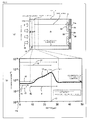
- Fig. 3(a) is a cross-sectional view illustrating a main portion of the IGBT 100 produced by the process flow shown in Fig. 1 and
- Fig. 3(b) is a diagram illustrating a carrier concentration profile in the vicinity of an n-type field stop layer 3.
- the method for producing the semiconductor device according to Embodiment 1 of the invention will be described with reference to the process flow of Fig. 1 and the cross-sectional view of Fig. 3(a) .
- a MOS gate structure including, for example, a p base layer 22, an n emitter layer 2, a gate insulating film 23, a gate electrode 24, and an interlayer insulating film 28 is formed on one main surface (front surface 11a) of an n semiconductor substrate (wafer) 11.
- the n emitter layer 2 is formed in the p base layer 22.
- the configuration of the MOS gate structure will be described below.
- an emitter electrode 25 which is a metal film that commonly comes into conductive contact with the surfaces of both the p base layer 22 and the n emitter layer 2 and is also a surface electrode, is formed.
- the metal material forming the emitter electrode 25 include A1 (aluminum), an A1 alloy, such as Al-Si (silicon) or Al-Cu (copper), Cu, Au (gold), and Ni (nickel).
- a surface protective film which protects a front surface 11a is formed.
- the surface protective film is made of a protective tape, a photoresist, or polyimide.
- a rear surface grinding process shown in Fig. 1(d) a rear surface 11b of the n semiconductor substrate 11 (n drift layer 1) is ground (back grinding) to a predetermined thickness which is determined by the relationship with a breakdown voltage.
- proton implantation 16 is performed from a rear surface 11b.
- the irradiation energy of the proton implantation 16 is selected to form the n-type field stop layer 3 at a predetermined depth.
- the projected range Rp of the implanted protons from the rear surface 11b (ground surface) is deeper than 15 ⁇ m. In some cases, the projected range Rp is in the projected range of 20 ⁇ m to 400 ⁇ m depending on the rated voltage. Specifically, the projected range Rp of the implanted proton from the rear surface 11b (the ground surface) is, for example, in the projected range of 20 ⁇ m to 60 ⁇ m.
- the depth of the FS layer, which is formed at the deepest position from the rear surface 11b, according to the rated voltage will be described below.
- furnace annealing is performed to the n-type field stop layer 3 using the change of protons into donors.
- the furnace annealing process puts a wafer into a constant-temperature furnace, such as an electric furnace with a constant temperature and performs a heat treatment to heat the entire wafer.
- the processing temperature of the furnace annealing process is in the range of 350°C to 550°C and the processing time thereof is in the range of 1 to 10 hours. In the temperature range, crystal defects remain in the projected range Rp of protons and a proton passage region 14 and the formation of hydrogen-induced donors by the proton implantation 16 is accelerated.
- disorder which is introduced by the proton implantation 16 also remains in the proton passage region 14(a region from a proton implantation surface to the projected range Rp) to form a disorder region 15.
- the remaining disorder is the generation center of carriers which cause a reduction in the mobility of the carriers or a leakage current.
- boron ions are implanted into the rear surface 11b.
- the boron ion implantation is performed for a surface layer of the rear surface 11b such that the projected range (Rp) of the protons from the rear surface is shallow.
- a laser annealing process shown in Fig. 1(h) laser light is radiated to the rear surface 11b for which the proton implantation 16 has been performed to reduce the disorder which remains in the furnace annealing, thereby forming an n-type disorder reduction region 18, and to activates the boron implanted into the shallow portion from the rear surface 11b, thereby forming a p collector layer 4.
- the laser annealing process heats the projected range Rp of the protons radiated to the rear surface 11b using, for example, a YAG laser.
- the pulse width (half width) of the laser light is in the range of, for example, 300 ns to 800 ns and the laser light is radiated to the same portion several times.
- the temperature of silicon in the irradiation portion is about 3000°C, but a heating time and a cooling time are very short (an order of 10 ns to 1 ⁇ s).
- the penetration depth of the laser light is within the penetration depth (projected range Rp) of the protons.
- the wavelength of the laser light is selected such that the penetration depth is from the position of the base (the end 3a of the n-type field stop layer 3 close to the rear surface 11b) of a mountain (convex portion) with the peak of donor generation concentration (carrier concentration) by the protons, which is close to the rear surface 11b, to a proton implantation surface (rear surface 11b) (a portion of the proton passage region 14). It is preferable that the wavelength of the laser light be in the range of 10 ⁇ m to 1000 ⁇ m.
- the temperature of the portion irradiated with the laser light is equal to or higher than 1000°C. In this case, it is possible to effectively form the n-type disorder reduction region 18. It is preferable that the temperature be equal to or higher than 2000°C and equal to or lower than the boiling point (3266°C) of Si. In particular, the temperature is not higher than the melting point of silicon. In this case, it is possible to prevent the ablation (surface roughness) of the irradiation surface after laser irradiation. In addition, a lamp annealing process may be performed, instead of the laser annealing process. The above-mentioned process makes it possible to form the n-type disorder reduction region 18 between the proton implantation surface and the projected range (Rp).
- a collector electrode (not shown) which comes into conductive contact with the surface of the p collector layer 4 is formed by, for example, vacuum sputtering.
- a metal annealing process is performed, if necessary.
- the point of the production method according to this embodiment is to perform both the furnace annealing process and the laser annealing process. The effect of this method will be described below.
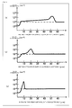
- Fig. 11 is a graph illustrating the comparison among the carrier concentration distributions for each projected range Rp of the proton implantation which is around 15 ⁇ m when a sample is formed only by furnace annealing.
- Fig. 11(a) shows a case in which the projected range Rp is 50 ⁇ m
- Fig. 11(b) shows a case in which the projected range Rp is 20 ⁇ m
- Fig. 11(c) shows a case in which the projected range Rp is 10 ⁇ m.
- the furnace annealing temperature is 400°C.
- the carrier concentration is greatly reduced at a depth of about 5 ⁇ m from the implantation surface in any projected range Rp.
- a disorder remains at a depth of about 5 ⁇ m from the implantation surface, and it is difficult to recover carrier mobility in a region in the vicinity of the implantation surface when only the furnace annealing is performed.
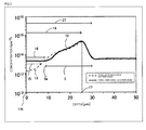
- Fig. 2 shows the verification results of the carrier concentration profile in the vicinity of the n-type field stop layer 3 when the laser annealing process is performed and when the laser annealing process is not performed.
- Fig. 2 shows carrier concentration profiles 12 and 13 in the vicinity of the n-type field stop layer 3 when the laser annealing process is performed and when the laser annealing process is not performed, respectively.
- the furnace annealing process (here, 400°C) is performed.
- the disorder which remains in the furnace annealing is reduced by the laser annealing process to form the n-type disorder reduction region 18.
- the carrier concentration profile 12 shown in Fig. 2 is obtained after the n-type disorder reduction region 18 is formed.
- the carrier concentration profile 13 when the laser annealing process is not performed and the disorder remains is represented by a dotted line.
- the projected range Rp of protons is 25 ⁇ m and the corresponding acceleration energy of the protons is 1.35 MeV.
- the energy density of the laser annealing process is 2.8 J/cm 2 .
- a disorder region 15 is spread in a region (a portion of the proton passage region 14) between the base (that is, the end 3a of the n-type field stop layer 3 close to the rear surface 11b) of the peak (mountain), which is the projected range 17 (Rp) of the proton, to the proton implantation surface (rear surface 11b).
- the end 3a of the base of the peak (mountain) close to the rear surface 11b is at a depth of about 5 ⁇ m from the implantation surface.
- the carrier concentration of a portion of the proton passage region 14 from the implantation surface (rear surface 11b) to the end 3a of the n-type field stop layer 3 close to the rear surface 11b is substantially equal to the concentration of the silicon substrate which is deeper than the projected range 17. That is, the disorder which remains in the proton passage region 14 when only the furnace annealing process is performed is reduced by both the laser annealing process and the furnace annealing process.
- the region in which the disorder is reduced is referred to as the n-type disorder reduction region 18.
- a pair of one n-type field stop layer 3 and one n-type disorder reduction region 18 which is adjacent to the implantation surface is referred to as an n-type intermediate layer 27.
- the carrier concentration is reduced in the disorder region 15. That is, in the carrier concentration profile 13 when the laser annealing process is not performed which is represented by a dotted line in Fig. 2 , apparently, the carrier concentration is reduced in the disorder region 15 before the n-type field stop layer 3 is formed (at a position shallower than the n-type field stop layer 3 from the rear surface).
- the apparent reduction in the carrier concentration is caused by a conversion method which calculates resistivity from the spreading resistance measured by the known spreading resistance method (SR method) and converts the resistivity into carrier concentration. That is, in the disorder region 15 in which a crystal lattice is disordered, electrons or holes are scattered by strong disorder, which results in a reduction in the mobility of the carriers.
- SR method spreading resistance method
- the calculation of carrier concentration is affected by a reduction in the mobility of carriers by the disorder region 15 as follows.
- the electron mobility of silicon at room temperature (about 300K) is 1360 (cm 2 /V ⁇ s) and the hole mobility thereof is 495 (cm 2 /V ⁇ s).
- the mobility of carriers does not contribute to converting spreading resistance into resistivity.
- ⁇ is the mobility of electrons or holes (cm 2 /V ⁇ s) and q is an elementary charge (1.6 ⁇ 10 -19 C).
- carrier concentration N is calculated to be small since the resistivity ⁇ 0 is a constant value. This appears as an apparent reduction in carrier concentration in the carrier concentration profile 13 when the laser annealing process is not performed as shown in Fig. 2 .
- the disorder of the disorder region 15 which is formed in the proton passage region 14 on the side of the rear surface 11b is reduced by the laser annealing process to form the n-type disorder reduction region 18, electrical characteristics, such as a leakage current, are improved.
- the furnace annealing process is needed in order to increase the donor generation rate of the hydrogen-induced donor.
- the laser annealing process is needed in order to reduce the disorder which remains in the proton passage region 14 and to form the n-type disorder reduction region 18.
- the furnace annealing process may be performed in the above-mentioned temperature range and the processing time range.
- the pn junction plane of the p collector layer be flat.
- the pn junction plane corresponds to the shape of the roughness.
- the energy density is two low, the disorder in the vicinity of the implantation surface (a depth of 5 ⁇ m from the implantation surface) is not sufficiently removed, but remains. As a result, carrier mobility is reduced.
- the results of the inventors' research proved that the sum of the energy density of the laser irradiation surface in laser annealing was preferably equal to or greater than 1 J/cm 2 and equal to or less than 4J/cm 2 .
- Fig. 2 can verify to what extent the carrier mobility in the n-type disorder reduction region 18 can be recovered.
- the carrier concentration of the n semiconductor substrate 11 is about 6 ⁇ 10 13 (/cm 3 ).
- the carrier concentration of a portion (a portion of the proton passage region) from the implantation surface to a depth of 5 ⁇ m is about 5 ⁇ 10 (/cm 3 ) and is recovered up to 83% of the substrate concentration. That is, this shows that the carrier mobility is recovered up to about 83% of the theoretical value of a crystal.
- the carrier mobility is about 1.2 ⁇ 10 13 (/cm 3 ) in the implantation surface with the lowest carrier concentration and is reduced to about 20%.
- the minimum value of the carrier mobility in the n-type disorder reduction region 18 depends on the reduction state of conduction loss (the saturated voltage V CE (sat) of the IGBT).
- the minimum value of the carrier mobility is equal to or greater than 20% of the theoretical value of the crystal state and preferably equal to or greater than 50% of the theoretical value. In this case, the influence of the minimum value of the carrier mobility is negligible, as compared to the conduction loss when the carrier mobility is not reduced.
- the upper limit of the minimum value of the carrier mobility in the n-type disorder reduction region 18 is preferably 100% of the theoretical value of the crystal state.
- the temperature of the furnace annealing process be equal to or higher than 350°C and equal to or lower than 550°C.
- the temperature is lower than 350°C, disorder remains in the entire proton implantation region from the implantation surface to the projected range Rp and the minimum value of the carrier mobility is less than 10%.
- the temperature is equal to or higher than 550°C, the hydrogen-induced donor disappears.
- the temperature is more preferably equal to or higher than 380°C and equal to or lower than 450°C and most preferably equal to or higher than 400°C and equal to or lower than 420°C. In this case, it is possible to achieve both the formation of the hydrogen-induced donor and the suppression of a reduction in carrier mobility.
- the carrier concentration of the n-type disorder reduction region 18 is lower than the concentration of the n-type field stop layer 3 and is higher than the concentration of the n semiconductor substrate 11. This is because the hydrogen ion remaining in the proton passage region 14 and the neighboring point defect form a composite defect. In this case, when the concentration of the proton passage region 14 is equal to or higher than the concentration of the n semiconductor substrate 11, disorder is reduced in the n-type disorder reduction region 18.
- the p base layer 22 is formed in the front surface 11a of the n semiconductor substrate 11 and the n emitter layer 2 is formed in a surface layer of the p base layer 22.
- the gate electrode 24 is formed on a portion of the p base layer 22 which is interposed between the n emitter layer 2 and the n semiconductor substrate 11, with the gate insulating film 23 interposed therebetween.
- the gate electrode 24, the gate insulating film 23, the n semiconductor substrate 11, and the n emitter layer 2 form the MOS gate structure.
- the interlayer insulating film 28 is formed on the gate electrode 24 and the emitter electrode 25 which comes into conductive contact with the n emitter layer 2 and the p base layer 22 is formed on the interlayer insulating film 28.
- the n-type field stop layer 3 with a higher carrier concentration than the n semiconductor substrate 11 is formed in the rear surface 11b of the n semiconductor substrate 11 by proton implantation and furnace annealing.
- the p collector layer 4 and the n-type disorder reduction region 18 are formed at a position that is shallower than the n-type field stop layer 3 by boron ion implantation and a laser annealing process for reducing disorder.
- a collector electrode (not shown) is formed on the p collector layer 4. In this way, the IGBT 100 is completed.
- the n semiconductor substrate 11 from the n-type field stop layer 3 to the p base layer 22 is the n drift layer 1 in which the main current flows to maintain the main breakdown voltage.
- Fig. 12 is a cross-sectional view illustrating the IGBT according to the invention.
- a leakage stop layer 32 with concentration that is higher than that of the n-type field stop layer 3 and is lower than that of the p collector layer 4 may be formed between the p collector layer 4 and the n-type disorder reduction region 18.
- the leakage stop layer 32 is formed by, for example, phosphorus ion implantation.
- the n-type field stop layer 3 of the IGBT 100 is formed by performing the proton implantation 16 from the rear surface 11b and performing the furnace annealing process such that an appropriate number of crystal defects, thereby changing protons into donors.
- the formation of the n-type disorder reduction region 18 by a reduction in the disorder formed by the proton passage region 14 is effectively performed by the laser annealing process of radiating laser light to the rear surface 11b.
- the IGBT 100 shown in Fig. 3 and the IGBT 100 shown in Fig. 12 have different MOS gate structures ( Fig. 3 shows a planar gate structure and Fig. 12 shows a trench gate structure).
- n-type intermediate layer 27 formed by a pair of the n-type field stop layer 3 and the n-type disorder reduction region 18 is formed in the rear surface 11b, the two structures have the same effect.
- the structure which includes two or more n-type intermediate layers 27 as shown in Fig. 12 will be described below.
- reference numeral 22 denotes a p base layer
- reference numeral 23 denotes a gate insulating film
- reference numeral 24 denotes a gate electrode
- reference numeral 25 denotes an emitter electrode
- reference numeral 28 denotes an interlayer insulating film.
- reference numeral 33 denotes a collector electrode.
- FIG. 4 is a process flow illustrating a method for producing the semiconductor device according to Embodiment 2 of the invention.
- Embodiment 2 differs from Embodiment 1 in that proton implantation is followed by boron implantation (a process of Fig. 4(e) ) and then a laser annealing process (a process of Fig. 4(f) ) and a furnace annealing process (a process of Fig. 4(g) ) are sequentially performed.
- boron is activated to form the p collector layer 4 at the same time as the n-type disorder reduction region 18 is formed in the proton passage region 14 formed by the proton implantation 16.
- the furnace annealing process which is a post-process, protons are changed into donors to form the n-type field stop layer 3.
- the n-type disorder reduction region 18 is formed by a combination of the laser annealing process and the furnace annealing process and the donor generation rate increases to form the n-type field stop layer 3.
- the formation of the n-type disorder reduction region makes it possible to improve electrical characteristics, such as the leakage current of the semiconductor device.
- the front surface 11a opposite to the proton implantation surface (rear surface 11b) shown in Fig. 3 is covered with a protective film, the protective film is removed after the proton implantation 16, and furnace annealing is performed. Then, a second protective film as a protective film for second boron ion implantation is formed and laser annealing is performed. That is, the protective film needs to be formed two times.
- the process of removing the protective film may be performed only once. Therefore, it is possible to reduce manufacturing costs, as compared to the process flow shown in Fig. 1 .
- the semiconductor device (IGBT 100) produced by the process flow shown in Fig. 4 has the same structure as that shown in Fig. 3 .
- the semiconductor device according to Embodiment 3 is an IGBT including one or more n-type intermediate layers 27 each including a pair of an n-type field stop layer 3 and an n-type disorder reduction region 18. For example, in this embodiment, three n-type intermediate layers 27 are formed.
- Fig. 5(a) is a cross-sectional view illustrating a main portion of the semiconductor device (IGBT 100) according to Embodiment 3 of the invention and
- Fig. 5(b) is a diagram illustrating a carrier concentration profile in the vicinity of the n-type field stop layer 3.
- Fig. 8 shows the turn-off oscillation waveform of a general IGBT.
- a collector current is equal to or less than one-tenth of the rated current, in some cases, the number of carriers accumulated is small and oscillation occurs before the turning-off of the IGBT ends.
- the collector current is fixed to a certain value and the IGBT is turned off by a different power supply voltage V CC .
- the power supply voltage V CC is greater than a predetermined value, it is greater than the peak value of a general overshoot voltage in the voltage waveform between the collector and the emitter and an additional overshoot occurs.
- the additional overshoot (voltage) serves as a trigger and the subsequent waveform oscillates.
- an oscillation start threshold value V RRO a threshold voltage at which the voltage waveform starts to oscillate.
- the oscillation start threshold value V RRO depends on the position of a first proton peak that a depletion layer (strictly, a space charge region since there is a hole), which is spread from the pn junction between a p base layer and an n drift layer of the IGBT to the n drift layer, reaches first, among a plurality of proton peaks.
- the reason is as follows.
- the depletion layer is spread from the pn junction between the p base layer and the n drift layer to the n drift layer at the time the IGBT is turned off, the end of the depletion layer reaches the first field stop (FS) layer (closest to the p base layer) and the spreading of the depletion layer is suppressed.
- the sweep of the accumulated carriers is weakened. As a result, the depletion of the carriers is suppressed and oscillation is suppressed.
- the depletion layer is spread from the pn junction between the p base layer and the n drift layer (hereinafter, simply referred to as the pn junction) toward the collector electrode in the depth direction. Therefore, the peak position of the FS layer which the end of the depletion layer reaches first is the FS layer which is closest to the pn junction.
- the thickness of the n semiconductor substrate (the thickness of a portion interposed between the emitter electrode and the collector electrode) is W0 and the depth of the peak position of the FS layer which the end of the depletion layer reaches first from the interface between the collector electrode and the rear surface of the n semiconductor substrate 11 (hereinafter, referred to as a distance from the rear surface) is X.
- a distance index L is introduced.
- the distance index L is represented by the following Expression (1).
- L ⁇ S ⁇ V rate J F q ⁇ v sat + N d
- the distance index L represented by the above-mentioned Expression (1) is an index indicating the distance of the end (depletion layer end) of the depletion layer (exactly, a space charge region), which is spread from the pn junction to the n drift layer 1, from the pn junction when a voltage V CE between the collector and the emitter is a power supply voltage V CC at the time the IGBT is turned off.
- a denominator indicates the space charge density of the space charge region (depletion layer) when the IGBT is turned off.
- q is an elementary charge
- p hole concentration
- n electron concentration
- N d donor concentration
- N a acceptor concentration
- ⁇ S is the permittivity of a semiconductor.
- the donor concentration N d is average concentration obtained by integrating the n drift layer in the depth direction and dividing the integrated value by the distance of the integrated section.
- the net doping concentration shown in Fig. 13(b) is the net doping concentration of N d -N a and the axis indicates the absolute value of N d -N a .
- the space charge density p is described by the hole concentration p passing through the space charge region (depletion layer) when the IGBT is turned off and the average donor concentration N d of the n drift layer.
- the electron concentration is lower than these concentrations so as to be negligible and there is no acceptor. Therefore, ⁇ ⁇ q (p+N d ) is established.
- the hole concentration p is determined by a breaking current of the IGBT.
- J F is the rated current density of the element
- v sat is a saturated velocity in which the speed of the carrier is saturated with predetermined electric field intensity.
- the length x of the space charge region obtained when the voltage V is half of the rated voltage V rate is the distance index L. This is because an operation voltage (power supply voltage), which is the voltage V, is about half of the rated voltage in the actual device such as an inverter. Since the doping concentration of the FS layer is higher than that of the n drift layer, the FS layer prevents the expansion of the space charge region which is spread at the time the IBGT is turned off.
- Fig. 10 is a table illustrating the position conditions of the FS (field stop) layer which the depletion layer reaches first in the semiconductor device according to the invention.
- FIG. 10 shows the distance X of the peak position of the FS layer which the end of the depletion layer reaches first from the rear surface at a rated voltage of 600 V to 6500 V.
- X W0- ⁇ L is established and ⁇ is a coefficient.
- Fig. 10 shows the distance X when ⁇ is changed from 0.7 to 1.6.
- the element is safely designed so as to have a breakdown voltage which is about 10% higher than the rated voltage.
- the total thickness of the n semiconductor substrate (the thickness during a finishing process after the n semiconductor substrate is thinned by, for example, grinding) and the average resistivity of the n drift layer are set such that an on-voltage or turn-off loss is sufficiently reduced.
- the term 'average' means the average concentration and resistivity of the entire n drift layer including the FS layer.
- the rated current density has the typical value shown in Fig. 10 due to the rated voltage.
- the rated current density is set such that energy density which is determined by the product of the rated voltage and the rated current density has a substantially constant value and has nearly the value shown in Fig. 10 .
- the distance index L is calculated using these values according the above-mentioned Expression (1), the value shown in Fig. 10 is obtained.
- the distance X of the peak position of the FS layer which the end of the depletion layer reaches first from the rear surface is obtained by subtracting the product of the distance index L and ⁇ , which is in the range of 0.7 to 1.6, from the thickness W0 of the n semiconductor substrate 11.
- Fig. 7 is a characteristic diagram illustrating a threshold voltage at which the voltage waveform starts to oscillate. Specifically, Fig. 7 is a graph illustrating the dependence of V RRO on y at some typical rated voltages V rate (600 V, 1200 V, and 3300 V). In Fig. 7 , the vertical axis indicates a value obtained by standardizing V RRO with the rated voltage V rate . As can be seen from Fig. 7 , V RRO can be rapidly increased at three rated voltages when ⁇ is equal to or less than 1.6.
- V CC power supply voltage
- V RRO /V rate the value of V RRO /V rate needs to be equal to or greater than 0.5.
- the value of V RRO /V rate is equal to or greater than 0.5 at ⁇ of 0.2 to 1.5. Therefore, it is preferable that ⁇ be in the range of at least 0.2 to 1.5.
- V RRO /V rate does not greatly from three curves and has the same dependence (the value of V RRO with respect to ⁇ ).
- ⁇ is in the range of 0.7 to 1.4, it is possible to sufficiently increase V RRO at any rated voltage.
- ⁇ is less than 0.7, the avalanche breakdown voltage of the element is likely to be lower than the rated voltage since V RRO is equal to or higher than about 80% of the rated voltage, but the FS layer is close to the p base layer. Therefore, it is preferable that ⁇ be equal to or greater than 0.7.
- ⁇ is greater than 1.4, V RRO is rapidly reduced from about 70% and turn-off oscillation is likely to occur. Therefore, it is preferable that ⁇ be equal to or less than 1.4.
- ⁇ is more preferably in the range of 0.8 to 1.3 and most preferably in the range of 0.9 to 1.2. In this case, it is possible to maximize V RRO while sufficiently increasing the avalanche breakdown voltage of the element to be higher than the rated voltage.
- the range of ⁇ capable of sufficiently increasing V RRO is substantially the same (0.7 to 1.4) at any rated voltage.
- the distance (depth) of the end of the space charge region is about the distance index L represented by the above-mentioned Expression (1).
- the peak position of the FS layer which is deepest from the rear surface is the position of L (that is, ⁇ is about 1.0)
- the coefficient ⁇ of the distance index L may be in the above-mentioned range at any rated voltage. In this case, it is possible to effectively suppress the oscillation phenomenon when the IGBT is turned off.
- the distance index L is more than a depth of 20 ⁇ m at any rated voltage. That is, the projected range Rp1 of the protons for forming the first proton peak is deeper than 15 ⁇ m from the rear surface of the substrate and is equal to or more than 20 ⁇ m in order to maximize the effect of suppressing oscillation.
- the acceleration energy of protons in a method for producing a semiconductor device according to Embodiment 5 of the invention will be described.
- the acceleration energy of the protons may be determined from the characteristic graph shown in Fig. 9 in order to form an FS layer which a depletion layer reaches first and which has a peak position that is at a distance X from the rear surface, using proton irradiation, such that the above-mentioned range of ⁇ is satisfied in practice.
- Fig. 9 is a characteristic diagram illustrating the relationship between the projected range of the protons and the acceleration energy of the protons in the semiconductor device according to the invention.
- Fig. 9 is a characteristic graph indicating the above-mentioned Expression (2).
- Fig. 9 shows the acceleration energy of the protons for obtaining the desired projected range of the protons.
- the horizontal axis is the logarithm log(Rp) of the projected range Rp of the protons and indicates the projected range Rp ( ⁇ m) corresponding to the parentheses below the axis value of log(Rp).
- the vertical axis is the logarithm log(E) of the acceleration energy E of the protons and indicates the acceleration energy E of the protons corresponding to the parentheses on the left side of the axis value of log(E).
- the following relationship may be considered between the actual acceleration energy E' and an average projected range Rp' (proton peak position) which is actually obtained by, for example, the spreading resistance (SR) method when the above-mentioned fitting equation is used to calculate the acceleration energy E of proton irradiation from the desired average projected range Rp of the protons and the protons are implanted into a silicon substrate with the calculated value of the acceleration energy.
- SR spreading resistance
- the actual average projected range Rp' is within the range of about ⁇ 10% of the desired average projected range Rp and is in a measurement error range. Therefore, the influence of a variation in the actual average projected range Rp' from the desired average projected range Rp on the electrical characteristics of an IGBT is so small to be negligible.
- the actual acceleration energy E' is in the range of ⁇ 10% of the calculated value E, it is possible to determine that the actual average projected range Rp' is substantially equal to the set average projected range Rp.
- the actual average projected range Rp' is in the range of about ⁇ 10% of the average projected range Rp obtained by applying the actual acceleration energy E' to the above-mentioned Expression (2), no problem occurs.
- a variation or error range may be equal to or less than ⁇ 10% of the average projected range Rp.
- the variation or error range is within the range of ⁇ 5%, it can be considered that the actual acceleration energy E' and the actual average projected range Rp' follow the above-mentioned Expression (2).
- the above-mentioned Expression (2) is used to calculate the acceleration energy E of the protons required to obtain the desired projected range Rp of the protons.
- the acceleration energy E of each proton for forming the FS layer is also calculated by the above-mentioned Expression (2) and is well matched with the value of a sample measured by the known spreading resistance measurement method (SR method) after proton irradiation is performed with the above-mentioned acceleration energy E'. Therefore, when the above-mentioned Expression (2) is used, it is possible to predict the required acceleration energy E of protons with high accuracy, on the basis of the projected range Rp of the protons.
- SR method spreading resistance measurement method
- FIG. 1 is an example of the process flow for producing the IGBT 100 and can be applied to a diode.
- the process of Fig. 1(a) is a process for forming an anode layer.
- boron is replaced with phosphorus or arsenic and a cathode layer is formed by the process of Fig. 1(f) .
- the cross-sectional view of the diode which is formed in this way is shown in Fig. 13.
- Fig. 13 is a cross-sectional view illustrating the diode according to the invention.
- a p anode layer 52 is formed in the front surface of a semiconductor substrate which will be an n drift layer 1 and an n cathode layer 53 is formed in the rear surface.
- Reference numeral 51 denotes an anode electrode and reference numeral 54 denotes a cathode electrode.
- the position or concentration of a field stop layer 3, an n-type disorder reduction region 18, and a n-type intermediate layer 27 which is a combination of the field stop layer 3 and the n-type disorder reduction region 18 is appropriately adjusted, similarly to the IGBT.
- the preferred position of the first proton peak position among a plurality of proton irradiation operations is the same as that in the IGBT when the turn-off oscillation is replaced with reverse recovery oscillation and the oscillation start threshold value V RRO is the threshold voltage of the power supply voltage V CC at which the voltage waveform of the diode starts to oscillate.
- the hydrogen ions implanted into the semiconductor substrate described as protons may be implanted.
- the range of the double hydrogen ions and the triple hydrogen ions is shorter than that of protons since the mass thereof is increased due to a neutron. Therefore, it is preferable to use protons in order to form the n-type intermediate layer 27 at a deep position from the surface of the semiconductor substrate.
- the semiconductor device and the method for producing the semiconductor device according to the invention are useful as power semiconductor devices used for power conversion apparatuses such as converters or inverters.
Landscapes
- Insulated Gate Type Field-Effect Transistor (AREA)
- Metal-Oxide And Bipolar Metal-Oxide Semiconductor Integrated Circuits (AREA)
- Physics & Mathematics (AREA)
- Electromagnetism (AREA)
- Optics & Photonics (AREA)
- Electrodes Of Semiconductors (AREA)
Applications Claiming Priority (2)
| Application Number | Priority Date | Filing Date | Title |
|---|---|---|---|
| JP2012009337 | 2012-01-19 | ||
| PCT/JP2013/051010 WO2013108911A1 (ja) | 2012-01-19 | 2013-01-18 | 半導体装置およびその製造方法 |
Publications (3)
| Publication Number | Publication Date |
|---|---|
| EP2806461A1 true EP2806461A1 (de) | 2014-11-26 |
| EP2806461A4 EP2806461A4 (de) | 2015-12-09 |
| EP2806461B1 EP2806461B1 (de) | 2021-11-24 |
Family
ID=48799332
Family Applications (1)
| Application Number | Title | Priority Date | Filing Date |
|---|---|---|---|
| EP13738600.9A Active EP2806461B1 (de) | 2012-01-19 | 2013-01-18 | Halbleiterbauelement und herstellungsverfahren dafür |
Country Status (5)
| Country | Link |
|---|---|
| US (3) | US9520475B2 (de) |
| EP (1) | EP2806461B1 (de) |
| JP (1) | JP5741716B2 (de) |
| CN (1) | CN103999225B (de) |
| WO (1) | WO2013108911A1 (de) |
Families Citing this family (28)
| Publication number | Priority date | Publication date | Assignee | Title |
|---|---|---|---|---|
| EP2790209B1 (de) | 2012-03-30 | 2019-09-25 | Fuji Electric Co., Ltd. | Herstellungsverfahren für halbleiterbauelement |
| CN104620391B (zh) * | 2012-10-23 | 2017-09-19 | 富士电机株式会社 | 半导体装置及其制造方法 |
| WO2014156849A1 (ja) * | 2013-03-25 | 2014-10-02 | 富士電機株式会社 | 半導体装置 |
| JP6037012B2 (ja) * | 2013-06-26 | 2016-11-30 | 富士電機株式会社 | 半導体装置および半導体装置の製造方法 |
| CN106062961B (zh) * | 2014-09-17 | 2020-02-11 | 富士电机株式会社 | 半导体装置以及半导体装置的制造方法 |
| JP6237921B2 (ja) * | 2014-09-30 | 2017-11-29 | 富士電機株式会社 | 半導体装置および半導体装置の製造方法 |
| CN105814694B (zh) * | 2014-10-03 | 2019-03-08 | 富士电机株式会社 | 半导体装置以及半导体装置的制造方法 |
| CN106463528B (zh) * | 2014-11-17 | 2019-10-11 | 富士电机株式会社 | 碳化硅半导体装置的制造方法 |
| CN107710417B (zh) * | 2015-06-16 | 2021-06-11 | 三菱电机株式会社 | 半导体装置的制造方法 |
| DE112017000064B4 (de) | 2016-02-23 | 2026-02-05 | Fuji Electric Co., Ltd. | Halbleitervorrichtung |
| JP6508099B2 (ja) * | 2016-03-18 | 2019-05-08 | 三菱電機株式会社 | 半導体素子 |
| KR102371864B1 (ko) * | 2016-04-27 | 2022-03-07 | 스미도모쥬기가이고교 가부시키가이샤 | 레이저어닐링방법 및 레이저어닐링장치 |
| WO2018092788A1 (ja) * | 2016-11-16 | 2018-05-24 | 富士電機株式会社 | 半導体装置 |
| US10170559B1 (en) * | 2017-06-29 | 2019-01-01 | Alpha And Omega Semiconductor (Cayman) Ltd. | Reverse conducting IGBT incorporating epitaxial layer field stop zone and fabrication method |
| CN110114861B (zh) | 2017-07-12 | 2022-05-31 | 富士电机株式会社 | 半导体装置的制造方法 |
| JP7143085B2 (ja) * | 2018-01-31 | 2022-09-28 | 三菱電機株式会社 | 半導体装置、電力変換装置及び半導体装置の製造方法 |
| DE112019000094T5 (de) | 2018-03-19 | 2020-09-24 | Fuji Electric Co., Ltd. | Halbleitervorrichtung und verfahren zum herstellen einerhalbleitervorrichtung |
| CN109712886A (zh) * | 2018-12-17 | 2019-05-03 | 成都森未科技有限公司 | 一种功率半导体器件的背面加工工艺 |
| WO2020149354A1 (ja) | 2019-01-18 | 2020-07-23 | 富士電機株式会社 | 半導体装置および半導体装置の製造方法 |
| JP6702467B2 (ja) * | 2019-02-25 | 2020-06-03 | 三菱電機株式会社 | 半導体装置及びその製造方法 |
| JP7375340B2 (ja) * | 2019-06-12 | 2023-11-08 | サンケン電気株式会社 | 半導体装置 |
| US11450734B2 (en) * | 2019-06-17 | 2022-09-20 | Fuji Electric Co., Ltd. | Semiconductor device and fabrication method for semiconductor device |
| EP3772749A1 (de) | 2019-08-08 | 2021-02-10 | Infineon Technologies Dresden GmbH & Co . KG | Verfahren und vorrichtungen in verbindung mit hochfrequenzvorrichtungen |
| DE112020001029B4 (de) | 2019-10-11 | 2025-06-05 | Fuji Electric Co., Ltd. | Halbleitervorrichtung und herstellungsverfahren einer halbleitervorrichtung |
| CN111682062A (zh) * | 2020-06-24 | 2020-09-18 | 全球能源互联网研究院有限公司 | 一种igbt器件的背面结构及其制备方法、igbt器件 |
| US11527618B2 (en) | 2020-07-18 | 2022-12-13 | Semiconductor Components Industries, Llc | Up-diffusion suppression in a power MOSFET |
| JP7601240B2 (ja) * | 2021-09-03 | 2024-12-17 | 富士電機株式会社 | 炭化珪素半導体装置および炭化珪素半導体基板 |
| JP2023135916A (ja) * | 2022-03-16 | 2023-09-29 | 富士電機株式会社 | 半導体装置 |
Family Cites Families (23)
| Publication number | Priority date | Publication date | Assignee | Title |
|---|---|---|---|---|
| JPS592346A (ja) * | 1982-06-28 | 1984-01-07 | Semiconductor Res Found | 半導体集積回路 |
| JPS61200872A (ja) | 1985-03-01 | 1986-09-05 | Toyo Seikan Kaisha Ltd | 防錆剤塗布装置 |
| JPH0627706B2 (ja) | 1985-04-25 | 1994-04-13 | オリンパス光学工業株式会社 | 反射率測定装置 |
| WO2000016408A1 (en) * | 1998-09-10 | 2000-03-23 | Mitsubishi Denki Kabushiki Kaisha | Semiconductor device and its manufacturing method |
| JP2001077357A (ja) * | 1999-08-31 | 2001-03-23 | Toshiba Corp | 半導体装置 |
| DE10055446B4 (de) | 1999-11-26 | 2012-08-23 | Fuji Electric Co., Ltd. | Halbleiterbauelement und Verfahren zu seiner Herstellung |
| JP3684962B2 (ja) | 1999-12-01 | 2005-08-17 | 富士電機デバイステクノロジー株式会社 | 半導体装置の製造方法 |
| DE10207522B4 (de) | 2001-02-23 | 2018-08-02 | Fuji Electric Co., Ltd. | Halbleiterbauelement und Verfahren zu dessen Herstellung |
| JP3951738B2 (ja) | 2001-02-23 | 2007-08-01 | 富士電機デバイステクノロジー株式会社 | 半導体装置の製造方法 |
| DE10349582B4 (de) | 2003-10-24 | 2008-09-25 | Infineon Technologies Ag | Halbleiterdiode sowie dafür geeignetes Herstellungsverfahren |
| DE102005026408B3 (de) | 2005-06-08 | 2007-02-01 | Infineon Technologies Ag | Verfahren zur Herstellung einer Stoppzone in einem Halbleiterkörper und Halbleiterbauelement mit einer Stoppzone |
| JP5201303B2 (ja) * | 2005-08-23 | 2013-06-05 | 富士電機株式会社 | 逆阻止型半導体装置の製造方法 |
| JP2007055352A (ja) | 2005-08-23 | 2007-03-08 | Calsonic Kansei Corp | 車両用表示装置及び組付方法 |
| JP5104314B2 (ja) * | 2005-11-14 | 2012-12-19 | 富士電機株式会社 | 半導体装置およびその製造方法 |
| US7989888B2 (en) * | 2006-08-31 | 2011-08-02 | Infineon Technologies Autria AG | Semiconductor device with a field stop zone and process of producing the same |
| DE102006046844B4 (de) * | 2006-10-02 | 2013-08-01 | Infineon Technologies Austria Ag | Leistungshalbleiterbauelement mit Feldstoppzone und Verfahren zur Herstellung eines solchen Leistungshalbleiterbauelements |
| JP5203667B2 (ja) | 2007-10-16 | 2013-06-05 | トヨタ自動車株式会社 | 半導体装置の製造方法 |
| JP5365009B2 (ja) * | 2008-01-23 | 2013-12-11 | 富士電機株式会社 | 半導体装置およびその製造方法 |
| US7932583B2 (en) * | 2008-05-13 | 2011-04-26 | Infineon Technologies Austria Ag | Reduced free-charge carrier lifetime device |
| JP5569532B2 (ja) * | 2009-11-02 | 2014-08-13 | 富士電機株式会社 | 半導体装置および半導体装置の製造方法 |
| WO2011111500A1 (ja) * | 2010-03-09 | 2011-09-15 | 富士電機システムズ株式会社 | 半導体装置 |
| US8466491B2 (en) * | 2011-05-12 | 2013-06-18 | Infineon Technologies Austria Ag | Semiconductor component with improved softness |
| US8809902B2 (en) * | 2011-10-17 | 2014-08-19 | Infineon Technologies Austria Ag | Power semiconductor diode, IGBT, and method for manufacturing thereof |
-
2013
- 2013-01-18 JP JP2013554375A patent/JP5741716B2/ja active Active
- 2013-01-18 CN CN201380004323.1A patent/CN103999225B/zh active Active
- 2013-01-18 EP EP13738600.9A patent/EP2806461B1/de active Active
- 2013-01-18 WO PCT/JP2013/051010 patent/WO2013108911A1/ja not_active Ceased
-
2014
- 2014-06-11 US US14/301,914 patent/US9520475B2/en active Active
-
2016
- 2016-10-07 US US15/288,132 patent/US9842918B2/en active Active
-
2017
- 2017-12-11 US US15/837,318 patent/US10128360B2/en active Active
Also Published As
| Publication number | Publication date |
|---|---|
| US9520475B2 (en) | 2016-12-13 |
| US10128360B2 (en) | 2018-11-13 |
| JPWO2013108911A1 (ja) | 2015-05-11 |
| CN103999225A (zh) | 2014-08-20 |
| US9842918B2 (en) | 2017-12-12 |
| WO2013108911A1 (ja) | 2013-07-25 |
| EP2806461B1 (de) | 2021-11-24 |
| US20170025520A1 (en) | 2017-01-26 |
| JP5741716B2 (ja) | 2015-07-01 |
| US20140291723A1 (en) | 2014-10-02 |
| US20180108765A1 (en) | 2018-04-19 |
| EP2806461A4 (de) | 2015-12-09 |
| CN103999225B (zh) | 2017-02-22 |
Similar Documents
| Publication | Publication Date | Title |
|---|---|---|
| US10128360B2 (en) | Semiconductor device and method for producing the same | |
| US11469297B2 (en) | Semiconductor device and method for producing semiconductor device | |
| US10720330B2 (en) | Semiconductor device and method of manufacturing semiconductor device | |
| US9466689B2 (en) | Method for manufacturing a semiconductor device and semiconductor device manufactured thereby | |
| US10050106B2 (en) | Manufacturing method for semiconductor device | |
| US9530672B2 (en) | Production method for a semiconductor device | |
| EP2793266A1 (de) | Halbleiterbauelement und herstellungsverfahren dafür |
Legal Events
| Date | Code | Title | Description |
|---|---|---|---|
| PUAI | Public reference made under article 153(3) epc to a published international application that has entered the european phase |
Free format text: ORIGINAL CODE: 0009012 |
|
| 17P | Request for examination filed |
Effective date: 20140819 |
|
| AK | Designated contracting states |
Kind code of ref document: A1 Designated state(s): AL AT BE BG CH CY CZ DE DK EE ES FI FR GB GR HR HU IE IS IT LI LT LU LV MC MK MT NL NO PL PT RO RS SE SI SK SM TR |
|
| DAX | Request for extension of the european patent (deleted) | ||
| RIC1 | Information provided on ipc code assigned before grant |
Ipc: H01L 29/739 20060101AFI20151028BHEP Ipc: H01L 21/336 20060101ALI20151028BHEP Ipc: H01L 29/08 20060101ALI20151028BHEP Ipc: H01L 29/78 20060101ALI20151028BHEP Ipc: H01L 21/268 20060101ALI20151028BHEP |
|
| RA4 | Supplementary search report drawn up and despatched (corrected) |
Effective date: 20151105 |
|
| STAA | Information on the status of an ep patent application or granted ep patent |
Free format text: STATUS: EXAMINATION IS IN PROGRESS |
|
| 17Q | First examination report despatched |
Effective date: 20180525 |
|
| RIC1 | Information provided on ipc code assigned before grant |
Ipc: H01L 29/08 20060101ALI20200408BHEP Ipc: H01L 21/268 20060101ALI20200408BHEP Ipc: H01L 29/739 20060101AFI20200408BHEP Ipc: H01L 29/36 20060101ALI20200408BHEP Ipc: H01L 21/336 20060101ALI20200408BHEP Ipc: H01L 29/78 20060101ALI20200408BHEP |
|
| GRAP | Despatch of communication of intention to grant a patent |
Free format text: ORIGINAL CODE: EPIDOSNIGR1 |
|
| STAA | Information on the status of an ep patent application or granted ep patent |
Free format text: STATUS: GRANT OF PATENT IS INTENDED |
|
| RIC1 | Information provided on ipc code assigned before grant |
Ipc: H01L 29/739 20060101AFI20210517BHEP Ipc: H01L 21/336 20060101ALI20210517BHEP Ipc: H01L 29/78 20060101ALI20210517BHEP Ipc: H01L 29/08 20060101ALI20210517BHEP Ipc: H01L 21/268 20060101ALI20210517BHEP Ipc: H01L 29/36 20060101ALI20210517BHEP Ipc: H01L 21/324 20060101ALI20210517BHEP |
|
| INTG | Intention to grant announced |
Effective date: 20210608 |
|
| GRAS | Grant fee paid |
Free format text: ORIGINAL CODE: EPIDOSNIGR3 |
|
| GRAA | (expected) grant |
Free format text: ORIGINAL CODE: 0009210 |
|
| STAA | Information on the status of an ep patent application or granted ep patent |
Free format text: STATUS: THE PATENT HAS BEEN GRANTED |
|
| AK | Designated contracting states |
Kind code of ref document: B1 Designated state(s): AL AT BE BG CH CY CZ DE DK EE ES FI FR GB GR HR HU IE IS IT LI LT LU LV MC MK MT NL NO PL PT RO RS SE SI SK SM TR |
|
| REG | Reference to a national code |
Ref country code: GB Ref legal event code: FG4D |
|
| RIN1 | Information on inventor provided before grant (corrected) |
Inventor name: KURIBAYASHI, HIDENAO Inventor name: TAKISHITA, HIROSHI Inventor name: YOSHIMURA, TAKASHI Inventor name: MIYAZAKI, MASAYUKI |
|
| REG | Reference to a national code |
Ref country code: AT Ref legal event code: REF Ref document number: 1450524 Country of ref document: AT Kind code of ref document: T Effective date: 20211215 |
|
| REG | Reference to a national code |
Ref country code: DE Ref legal event code: R096 Ref document number: 602013080176 Country of ref document: DE |
|
| REG | Reference to a national code |
Ref country code: IE Ref legal event code: FG4D |
|
| REG | Reference to a national code |
Ref country code: LT Ref legal event code: MG9D |
|
| REG | Reference to a national code |
Ref country code: NL Ref legal event code: MP Effective date: 20211124 |
|
| REG | Reference to a national code |
Ref country code: AT Ref legal event code: MK05 Ref document number: 1450524 Country of ref document: AT Kind code of ref document: T Effective date: 20211124 |
|
| PG25 | Lapsed in a contracting state [announced via postgrant information from national office to epo] |
Ref country code: RS Free format text: LAPSE BECAUSE OF FAILURE TO SUBMIT A TRANSLATION OF THE DESCRIPTION OR TO PAY THE FEE WITHIN THE PRESCRIBED TIME-LIMIT Effective date: 20211124 Ref country code: LT Free format text: LAPSE BECAUSE OF FAILURE TO SUBMIT A TRANSLATION OF THE DESCRIPTION OR TO PAY THE FEE WITHIN THE PRESCRIBED TIME-LIMIT Effective date: 20211124 Ref country code: FI Free format text: LAPSE BECAUSE OF FAILURE TO SUBMIT A TRANSLATION OF THE DESCRIPTION OR TO PAY THE FEE WITHIN THE PRESCRIBED TIME-LIMIT Effective date: 20211124 Ref country code: BG Free format text: LAPSE BECAUSE OF FAILURE TO SUBMIT A TRANSLATION OF THE DESCRIPTION OR TO PAY THE FEE WITHIN THE PRESCRIBED TIME-LIMIT Effective date: 20220224 Ref country code: AT Free format text: LAPSE BECAUSE OF FAILURE TO SUBMIT A TRANSLATION OF THE DESCRIPTION OR TO PAY THE FEE WITHIN THE PRESCRIBED TIME-LIMIT Effective date: 20211124 |
|
| PG25 | Lapsed in a contracting state [announced via postgrant information from national office to epo] |
Ref country code: IS Free format text: LAPSE BECAUSE OF FAILURE TO SUBMIT A TRANSLATION OF THE DESCRIPTION OR TO PAY THE FEE WITHIN THE PRESCRIBED TIME-LIMIT Effective date: 20220324 Ref country code: SE Free format text: LAPSE BECAUSE OF FAILURE TO SUBMIT A TRANSLATION OF THE DESCRIPTION OR TO PAY THE FEE WITHIN THE PRESCRIBED TIME-LIMIT Effective date: 20211124 Ref country code: PT Free format text: LAPSE BECAUSE OF FAILURE TO SUBMIT A TRANSLATION OF THE DESCRIPTION OR TO PAY THE FEE WITHIN THE PRESCRIBED TIME-LIMIT Effective date: 20220324 Ref country code: PL Free format text: LAPSE BECAUSE OF FAILURE TO SUBMIT A TRANSLATION OF THE DESCRIPTION OR TO PAY THE FEE WITHIN THE PRESCRIBED TIME-LIMIT Effective date: 20211124 Ref country code: NO Free format text: LAPSE BECAUSE OF FAILURE TO SUBMIT A TRANSLATION OF THE DESCRIPTION OR TO PAY THE FEE WITHIN THE PRESCRIBED TIME-LIMIT Effective date: 20220224 Ref country code: NL Free format text: LAPSE BECAUSE OF FAILURE TO SUBMIT A TRANSLATION OF THE DESCRIPTION OR TO PAY THE FEE WITHIN THE PRESCRIBED TIME-LIMIT Effective date: 20211124 Ref country code: LV Free format text: LAPSE BECAUSE OF FAILURE TO SUBMIT A TRANSLATION OF THE DESCRIPTION OR TO PAY THE FEE WITHIN THE PRESCRIBED TIME-LIMIT Effective date: 20211124 Ref country code: HR Free format text: LAPSE BECAUSE OF FAILURE TO SUBMIT A TRANSLATION OF THE DESCRIPTION OR TO PAY THE FEE WITHIN THE PRESCRIBED TIME-LIMIT Effective date: 20211124 Ref country code: GR Free format text: LAPSE BECAUSE OF FAILURE TO SUBMIT A TRANSLATION OF THE DESCRIPTION OR TO PAY THE FEE WITHIN THE PRESCRIBED TIME-LIMIT Effective date: 20220225 Ref country code: ES Free format text: LAPSE BECAUSE OF FAILURE TO SUBMIT A TRANSLATION OF THE DESCRIPTION OR TO PAY THE FEE WITHIN THE PRESCRIBED TIME-LIMIT Effective date: 20211124 |
|
| PG25 | Lapsed in a contracting state [announced via postgrant information from national office to epo] |
Ref country code: SM Free format text: LAPSE BECAUSE OF FAILURE TO SUBMIT A TRANSLATION OF THE DESCRIPTION OR TO PAY THE FEE WITHIN THE PRESCRIBED TIME-LIMIT Effective date: 20211124 Ref country code: SK Free format text: LAPSE BECAUSE OF FAILURE TO SUBMIT A TRANSLATION OF THE DESCRIPTION OR TO PAY THE FEE WITHIN THE PRESCRIBED TIME-LIMIT Effective date: 20211124 Ref country code: RO Free format text: LAPSE BECAUSE OF FAILURE TO SUBMIT A TRANSLATION OF THE DESCRIPTION OR TO PAY THE FEE WITHIN THE PRESCRIBED TIME-LIMIT Effective date: 20211124 Ref country code: EE Free format text: LAPSE BECAUSE OF FAILURE TO SUBMIT A TRANSLATION OF THE DESCRIPTION OR TO PAY THE FEE WITHIN THE PRESCRIBED TIME-LIMIT Effective date: 20211124 Ref country code: DK Free format text: LAPSE BECAUSE OF FAILURE TO SUBMIT A TRANSLATION OF THE DESCRIPTION OR TO PAY THE FEE WITHIN THE PRESCRIBED TIME-LIMIT Effective date: 20211124 Ref country code: CZ Free format text: LAPSE BECAUSE OF FAILURE TO SUBMIT A TRANSLATION OF THE DESCRIPTION OR TO PAY THE FEE WITHIN THE PRESCRIBED TIME-LIMIT Effective date: 20211124 |
|
| REG | Reference to a national code |
Ref country code: DE Ref legal event code: R097 Ref document number: 602013080176 Country of ref document: DE |
|
| PG25 | Lapsed in a contracting state [announced via postgrant information from national office to epo] |
Ref country code: MC Free format text: LAPSE BECAUSE OF FAILURE TO SUBMIT A TRANSLATION OF THE DESCRIPTION OR TO PAY THE FEE WITHIN THE PRESCRIBED TIME-LIMIT Effective date: 20211124 |
|
| REG | Reference to a national code |
Ref country code: CH Ref legal event code: PL |
|
| PLBE | No opposition filed within time limit |
Free format text: ORIGINAL CODE: 0009261 |
|
| STAA | Information on the status of an ep patent application or granted ep patent |
Free format text: STATUS: NO OPPOSITION FILED WITHIN TIME LIMIT |
|
| REG | Reference to a national code |
Ref country code: BE Ref legal event code: MM Effective date: 20220131 |
|
| GBPC | Gb: european patent ceased through non-payment of renewal fee |
Effective date: 20220224 |
|
| PG25 | Lapsed in a contracting state [announced via postgrant information from national office to epo] |
Ref country code: LU Free format text: LAPSE BECAUSE OF NON-PAYMENT OF DUE FEES Effective date: 20220118 Ref country code: AL Free format text: LAPSE BECAUSE OF FAILURE TO SUBMIT A TRANSLATION OF THE DESCRIPTION OR TO PAY THE FEE WITHIN THE PRESCRIBED TIME-LIMIT Effective date: 20211124 |
|
| 26N | No opposition filed |
Effective date: 20220825 |
|
| PG25 | Lapsed in a contracting state [announced via postgrant information from national office to epo] |
Ref country code: SI Free format text: LAPSE BECAUSE OF FAILURE TO SUBMIT A TRANSLATION OF THE DESCRIPTION OR TO PAY THE FEE WITHIN THE PRESCRIBED TIME-LIMIT Effective date: 20211124 Ref country code: BE Free format text: LAPSE BECAUSE OF NON-PAYMENT OF DUE FEES Effective date: 20220131 |
|
| PG25 | Lapsed in a contracting state [announced via postgrant information from national office to epo] |
Ref country code: LI Free format text: LAPSE BECAUSE OF NON-PAYMENT OF DUE FEES Effective date: 20220131 Ref country code: CH Free format text: LAPSE BECAUSE OF NON-PAYMENT OF DUE FEES Effective date: 20220131 |
|
| PG25 | Lapsed in a contracting state [announced via postgrant information from national office to epo] |
Ref country code: IE Free format text: LAPSE BECAUSE OF NON-PAYMENT OF DUE FEES Effective date: 20220118 Ref country code: GB Free format text: LAPSE BECAUSE OF NON-PAYMENT OF DUE FEES Effective date: 20220224 |
|
| PG25 | Lapsed in a contracting state [announced via postgrant information from national office to epo] |
Ref country code: IT Free format text: LAPSE BECAUSE OF FAILURE TO SUBMIT A TRANSLATION OF THE DESCRIPTION OR TO PAY THE FEE WITHIN THE PRESCRIBED TIME-LIMIT Effective date: 20211124 |
|
| PG25 | Lapsed in a contracting state [announced via postgrant information from national office to epo] |
Ref country code: HU Free format text: LAPSE BECAUSE OF FAILURE TO SUBMIT A TRANSLATION OF THE DESCRIPTION OR TO PAY THE FEE WITHIN THE PRESCRIBED TIME-LIMIT; INVALID AB INITIO Effective date: 20130118 |
|
| PG25 | Lapsed in a contracting state [announced via postgrant information from national office to epo] |
Ref country code: MK Free format text: LAPSE BECAUSE OF FAILURE TO SUBMIT A TRANSLATION OF THE DESCRIPTION OR TO PAY THE FEE WITHIN THE PRESCRIBED TIME-LIMIT Effective date: 20211124 Ref country code: CY Free format text: LAPSE BECAUSE OF FAILURE TO SUBMIT A TRANSLATION OF THE DESCRIPTION OR TO PAY THE FEE WITHIN THE PRESCRIBED TIME-LIMIT Effective date: 20211124 |
|
| PG25 | Lapsed in a contracting state [announced via postgrant information from national office to epo] |
Ref country code: TR Free format text: LAPSE BECAUSE OF FAILURE TO SUBMIT A TRANSLATION OF THE DESCRIPTION OR TO PAY THE FEE WITHIN THE PRESCRIBED TIME-LIMIT Effective date: 20211124 |
|
| PG25 | Lapsed in a contracting state [announced via postgrant information from national office to epo] |
Ref country code: MT Free format text: LAPSE BECAUSE OF FAILURE TO SUBMIT A TRANSLATION OF THE DESCRIPTION OR TO PAY THE FEE WITHIN THE PRESCRIBED TIME-LIMIT Effective date: 20211124 |
|
| REG | Reference to a national code |
Ref country code: DE Ref legal event code: R079 Ref document number: 602013080176 Country of ref document: DE Free format text: PREVIOUS MAIN CLASS: H01L0029739000 Ipc: H10D0012000000 |
|
| PGFP | Annual fee paid to national office [announced via postgrant information from national office to epo] |
Ref country code: FR Payment date: 20251128 Year of fee payment: 14 |
|
| PGFP | Annual fee paid to national office [announced via postgrant information from national office to epo] |
Ref country code: DE Payment date: 20251203 Year of fee payment: 14 |